EP4530060A1 - Dual interface laminated card and corresponding method for manufacturing a dual interface laminated card - Google Patents
Dual interface laminated card and corresponding method for manufacturing a dual interface laminated card Download PDFInfo
- Publication number
- EP4530060A1 EP4530060A1 EP24199993.7A EP24199993A EP4530060A1 EP 4530060 A1 EP4530060 A1 EP 4530060A1 EP 24199993 A EP24199993 A EP 24199993A EP 4530060 A1 EP4530060 A1 EP 4530060A1
- Authority
- EP
- European Patent Office
- Prior art keywords
- layer
- core plastic
- plastic layer
- layers
- dual interface
- Prior art date
- Legal status (The legal status is an assumption and is not a legal conclusion. Google has not performed a legal analysis and makes no representation as to the accuracy of the status listed.)
- Withdrawn
Links
Images

Classifications
-
- G—PHYSICS
- G06—COMPUTING OR CALCULATING; COUNTING
- G06K—GRAPHICAL DATA READING; PRESENTATION OF DATA; RECORD CARRIERS; HANDLING RECORD CARRIERS
- G06K19/00—Record carriers for use with machines and with at least a part designed to carry digital markings
- G06K19/06—Record carriers for use with machines and with at least a part designed to carry digital markings characterised by the kind of the digital marking, e.g. shape, nature, code
- G06K19/067—Record carriers with conductive marks, printed circuits or semiconductor circuit elements, e.g. credit or identity cards also with resonating or responding marks without active components
- G06K19/07—Record carriers with conductive marks, printed circuits or semiconductor circuit elements, e.g. credit or identity cards also with resonating or responding marks without active components with integrated circuit chips
- G06K19/077—Constructional details, e.g. mounting of circuits in the carrier
- G06K19/0772—Physical layout of the record carrier
- G06K19/07722—Physical layout of the record carrier the record carrier being multilayered, e.g. laminated sheets
-
- B—PERFORMING OPERATIONS; TRANSPORTING
- B32—LAYERED PRODUCTS
- B32B—LAYERED PRODUCTS, i.e. PRODUCTS BUILT-UP OF STRATA OF FLAT OR NON-FLAT, e.g. CELLULAR OR HONEYCOMB, FORM
- B32B27/00—Layered products comprising a layer of synthetic resin
- B32B27/06—Layered products comprising a layer of synthetic resin as the main or only constituent of a layer, which is next to another layer of the same or of a different material
- B32B27/08—Layered products comprising a layer of synthetic resin as the main or only constituent of a layer, which is next to another layer of the same or of a different material of synthetic resin
-
- B—PERFORMING OPERATIONS; TRANSPORTING
- B32—LAYERED PRODUCTS
- B32B—LAYERED PRODUCTS, i.e. PRODUCTS BUILT-UP OF STRATA OF FLAT OR NON-FLAT, e.g. CELLULAR OR HONEYCOMB, FORM
- B32B27/00—Layered products comprising a layer of synthetic resin
- B32B27/30—Layered products comprising a layer of synthetic resin comprising vinyl (co)polymers; comprising acrylic (co)polymers
- B32B27/304—Layered products comprising a layer of synthetic resin comprising vinyl (co)polymers; comprising acrylic (co)polymers comprising vinyl halide (co)polymers, e.g. PVC, PVDC, PVF, PVDF
-
- B—PERFORMING OPERATIONS; TRANSPORTING
- B32—LAYERED PRODUCTS
- B32B—LAYERED PRODUCTS, i.e. PRODUCTS BUILT-UP OF STRATA OF FLAT OR NON-FLAT, e.g. CELLULAR OR HONEYCOMB, FORM
- B32B27/00—Layered products comprising a layer of synthetic resin
- B32B27/32—Layered products comprising a layer of synthetic resin comprising polyolefins
-
- B—PERFORMING OPERATIONS; TRANSPORTING
- B32—LAYERED PRODUCTS
- B32B—LAYERED PRODUCTS, i.e. PRODUCTS BUILT-UP OF STRATA OF FLAT OR NON-FLAT, e.g. CELLULAR OR HONEYCOMB, FORM
- B32B3/00—Layered products comprising a layer with external or internal discontinuities or unevennesses, or a layer of non-planar shape; Layered products comprising a layer having particular features of form
- B32B3/02—Layered products comprising a layer with external or internal discontinuities or unevennesses, or a layer of non-planar shape; Layered products comprising a layer having particular features of form characterised by features of form at particular places, e.g. in edge regions
- B32B3/08—Layered products comprising a layer with external or internal discontinuities or unevennesses, or a layer of non-planar shape; Layered products comprising a layer having particular features of form characterised by features of form at particular places, e.g. in edge regions characterised by added members at particular parts
-
- B—PERFORMING OPERATIONS; TRANSPORTING
- B32—LAYERED PRODUCTS
- B32B—LAYERED PRODUCTS, i.e. PRODUCTS BUILT-UP OF STRATA OF FLAT OR NON-FLAT, e.g. CELLULAR OR HONEYCOMB, FORM
- B32B3/00—Layered products comprising a layer with external or internal discontinuities or unevennesses, or a layer of non-planar shape; Layered products comprising a layer having particular features of form
- B32B3/26—Layered products comprising a layer with external or internal discontinuities or unevennesses, or a layer of non-planar shape; Layered products comprising a layer having particular features of form characterised by a particular shape of the outline of the cross-section of a continuous layer; characterised by a layer with cavities or internal voids ; characterised by an apertured layer
-
- B—PERFORMING OPERATIONS; TRANSPORTING
- B32—LAYERED PRODUCTS
- B32B—LAYERED PRODUCTS, i.e. PRODUCTS BUILT-UP OF STRATA OF FLAT OR NON-FLAT, e.g. CELLULAR OR HONEYCOMB, FORM
- B32B7/00—Layered products characterised by the relation between layers; Layered products characterised by the relative orientation of features between layers, or by the relative values of a measurable parameter between layers, i.e. products comprising layers having different physical, chemical or physicochemical properties; Layered products characterised by the interconnection of layers
- B32B7/04—Interconnection of layers
- B32B7/12—Interconnection of layers using interposed adhesives or interposed materials with bonding properties
-
- G—PHYSICS
- G06—COMPUTING OR CALCULATING; COUNTING
- G06K—GRAPHICAL DATA READING; PRESENTATION OF DATA; RECORD CARRIERS; HANDLING RECORD CARRIERS
- G06K19/00—Record carriers for use with machines and with at least a part designed to carry digital markings
- G06K19/02—Record carriers for use with machines and with at least a part designed to carry digital markings characterised by the selection of materials, e.g. to avoid wear during transport through the machine
-
- G—PHYSICS
- G06—COMPUTING OR CALCULATING; COUNTING
- G06K—GRAPHICAL DATA READING; PRESENTATION OF DATA; RECORD CARRIERS; HANDLING RECORD CARRIERS
- G06K19/00—Record carriers for use with machines and with at least a part designed to carry digital markings
- G06K19/06—Record carriers for use with machines and with at least a part designed to carry digital markings characterised by the kind of the digital marking, e.g. shape, nature, code
- G06K19/067—Record carriers with conductive marks, printed circuits or semiconductor circuit elements, e.g. credit or identity cards also with resonating or responding marks without active components
- G06K19/07—Record carriers with conductive marks, printed circuits or semiconductor circuit elements, e.g. credit or identity cards also with resonating or responding marks without active components with integrated circuit chips
- G06K19/077—Constructional details, e.g. mounting of circuits in the carrier
- G06K19/07745—Mounting details of integrated circuit chips
-
- G—PHYSICS
- G06—COMPUTING OR CALCULATING; COUNTING
- G06K—GRAPHICAL DATA READING; PRESENTATION OF DATA; RECORD CARRIERS; HANDLING RECORD CARRIERS
- G06K19/00—Record carriers for use with machines and with at least a part designed to carry digital markings
- G06K19/06—Record carriers for use with machines and with at least a part designed to carry digital markings characterised by the kind of the digital marking, e.g. shape, nature, code
- G06K19/067—Record carriers with conductive marks, printed circuits or semiconductor circuit elements, e.g. credit or identity cards also with resonating or responding marks without active components
- G06K19/07—Record carriers with conductive marks, printed circuits or semiconductor circuit elements, e.g. credit or identity cards also with resonating or responding marks without active components with integrated circuit chips
- G06K19/077—Constructional details, e.g. mounting of circuits in the carrier
- G06K19/07749—Constructional details, e.g. mounting of circuits in the carrier the record carrier being capable of non-contact communication, e.g. constructional details of the antenna of a non-contact smart card
-
- B—PERFORMING OPERATIONS; TRANSPORTING
- B32—LAYERED PRODUCTS
- B32B—LAYERED PRODUCTS, i.e. PRODUCTS BUILT-UP OF STRATA OF FLAT OR NON-FLAT, e.g. CELLULAR OR HONEYCOMB, FORM
- B32B2272/00—Resin or rubber layer comprising scrap, waste or recycling material
-
- B—PERFORMING OPERATIONS; TRANSPORTING
- B32—LAYERED PRODUCTS
- B32B—LAYERED PRODUCTS, i.e. PRODUCTS BUILT-UP OF STRATA OF FLAT OR NON-FLAT, e.g. CELLULAR OR HONEYCOMB, FORM
- B32B2307/00—Properties of the layers or laminate
- B32B2307/70—Other properties
- B32B2307/75—Printability
-
- B—PERFORMING OPERATIONS; TRANSPORTING
- B32—LAYERED PRODUCTS
- B32B—LAYERED PRODUCTS, i.e. PRODUCTS BUILT-UP OF STRATA OF FLAT OR NON-FLAT, e.g. CELLULAR OR HONEYCOMB, FORM
- B32B2425/00—Cards, e.g. identity cards, credit cards
Definitions
- the present solution relates to a dual interface laminated card comprising a stack of layers, comprising an antenna inlay comprised between core plastic layers and a micromodule, and also to a corresponding method for the manufacturing of a dual interface laminated card.
- the solution may be applied to the manufacturing of chip cards, e.g. banking or transportation cards.
- Dual interface cards are known, which are cards, e.g. credit cards, with an embedded chip which allows both contact and contactless communication.
- credit card issuers are considering to incorporate recycled plastic in the fabrication of their cards.
- Conventional credit cards are manufactured from polyvinyl chloride (PVC), a synthetic polymer derived from oil.
- PVC polyvinyl chloride
- microplastics a synthetic polymer derived from oil.
- the utilization of recycled plastic counteracts the spread of plastic waste and confines carbon emissions, thereby contributing to the reduction of environmental contamination.
- a growing number of consumers are becoming increasingly aware of the environmental implications of their choices and thus prefer eco-friendly products, hence the provision of credit cards fabricated from recycled plastic aims to accommodate consumer preferences in this regard.
- a low surface energy plastic is here as a plastic with a surface energy up to 40 dyne/cm (or milliJoules/m 2 ), in variant embodiments up to 36 dyne/cm, in further variant embodiments below 36 dyne/cm.
- a minimum value may be 15 dyne/cm.
- the problem may be particularly relevant when the plastic sheet used for the card contains more than 80% of low surface energy plastic, e.g., r-HDPE, to obtain a card with a sufficient durability, e.g., at least three years, which is compliant with standards, such as CQM and Visa.
- low surface energy plastic e.g., r-HDPE
- an object of various embodiments of the present disclosure is to provide solutions that are able to overcome one or more of the limits of the prior art.
- one or more of the previous objects are achieved by a dual interface laminated card having the distinctive elements specified in the ensuing claims.
- the solution refers to a method for manufacturing such dual interface laminated card.
- a dual interface laminated card comprising a stack of layers, comprising at least:
- the card comprises a first layer of polyurethane heat activatable glue and a second layer of polyurethane heat activatable glue, respectively coupled to a side facing said antenna inlay of each of said first core plastic layer and second core plastic layer, bonding the antenna inlay and the core plastic layers together.
- the antenna inlay comprises only a layer of polyurethane heat activatable glue coupled to a side facing said antenna inlay of said first core plastic layer, bonding the antenna inlay and the first core plastic layer together.
- said micromodule is bonded to said second core plastic layer by means of a bi-adhesive material.
- it further comprises a bi-coated high surface energy material comprising a layer of high surface energy plastic, covered on both sides with an adhesive layer, placed in between the antenna inlay and the first layer of polyurethane heat activatable glue.
- said micromodule and said bi-adhesive material are received in a cavity obtained in the second core plastic layer, said cavity extending vertically along the entire thickness of the second core plastic layer, in particular from the side facing a second overlay layer to the side facing the bi-coated high surface energy material, said bi-adhesive material extending vertically along the entire depth of the cavity.
- the bi-adhesive material is a heat activatable bi-adhesive.
- the micromodule and the bi-adhesive material are received in a cavity obtained in the second core plastic layer, said cavity extending vertically from an upper side of the second core plastic layer to an inner portion of the second core plastic layer, said bi-adhesive material extending vertically along the entire depth of such cavity.
- the bi-adhesive material is a high bond acrylic glue or a bi-component epoxy resin.
- the card comprises a second overlay layer and a first overlay layer, wherein said overlay layers are printable and graphically customizable, in particular made in polyvinyl chloride.
- said layers comprising a major percentage, in particular at least 80%, of low surface energy plastic, said low surface energy plastic is substantially recycled high-density polyethylene.
- said low surface energy plastic is a recycled plastic with a surface energy up to 40 dyne/cm, in particular up to 36 dyne/cm, in further variant embodiments below 36 dyne/cm.
- said forming step comprises:
- said forming step comprises: depositing one layer of polyurethane heat activatable glue, respectively coupled to a side facing said antenna inlay of said second core plastic layer, in order to bond the antenna inlay and the core plastic layers together.
- said forming step further comprises applying a bi-coated high surface energy material between the antenna inlay and the first layer of polyurethane heat activatable glue.
- the method comprises arranging said micromodule and said bi-adhesive material in said cavity obtained in the first core plastic layer, said milling the card to obtain a cavity for embedding the micromodule comprising obtaining a cavity extending vertically along the entire thickness of the first core plastic layer, said bi-adhesive material extending vertically along the entire thickness of the first core plastic layer.
- the method comprises arranging said micromodule and said bi-adhesive material in said cavity obtained in the first core plastic layer, said cavity extending vertically from an upper side of the first core plastic layer to an inner portion of the first core plastic layer, said bi-adhesive material extending vertically along the entire depth of such cavity.
- a pretreatment by Corona or Plasma pre-treatment on the cavity is performed.
- the method comprises:
- a laminated card 100 comprises substantially a first core plastic layer 106, a second core plastic layer 102 arranged over said first core plastic layer 106, an antenna inlay 104 arranged between such first core plastic layer 106) and such first core plastic layer 102, a micromodule 108 arranged over said first core plastic layer 106.
- the card 100 comprises a plurality of stacked layers grouped in three parts: a front layers assembly 120, a back layers assembly 140 and in between a core assembly 130 comprising the antenna inlay 104 to provide contactless communication with a reader, here not shown, such as, for instance, a contactless Point Of Sale (POS), and a bi-coated high surface energy material layer 111.
- POS Point Of Sale
- Said bi-coated high surface energy material layer 111 comprises substantially a layer of high surface energy plastic, e.g., PVC, covered on both sides with an adhesive or glue to improve adhesion, in particular an adhesive effective on high energy surfaces such as PVC, i.e. with a similar surface energy, i.e. at least in the range of high surface energy over 40 dyne/cm, to bond in particular with the antenna inlay 104, which may be made of PVC.
- PVC high surface energy plastic
- the front layers assembly 120 comprises, from an inner to an external face i.e., the upper or front face of the laminated card 100, a second core plastic layer 102, in which is obtained a cavity 102a, which in the embodiment shown is passing through the entire thickness of the second core plastic layer 102, a bi-adhesive material 110 filling such cavity 102a.
- the bi-adhesive material 110 may be a Hot Melt Adhesive (HMA).
- HMA Hot Melt Adhesive
- a Hot Melt or Hotmelt adhesive is usually a glue tape, heat activated double-sided film used for the embedding of chip modules into smartcard.
- a micromodule 108 Over the second core plastic layer 102, in the region of the bi-adhesive material 110 is placed a micromodule 108, over which is placed a second overlay layer 101.
- An array of electrical contacts 109 is coupled to the micromodule 108, arranged in an opening of the second overlay layer 101.
- the second core plastic layer 102 can be made of a recycled plastic material, such as recycled high-density polyethylene (r-HDPE), or also recycled polyethylene terephthalate (r-PET). Such recycled materials can exhibit a low surface energy i.e., they can have a surface energy smaller up to 40 dyne/cm.
- r-HDPE recycled high-density polyethylene
- r-PET recycled polyethylene terephthalate
- the bi-adhesive material 110 extends from the bi-coated high surface energy material 111, which represents the upper layer of the core assembly 130 to the micromodule 108 above, it is configured to embed the micromodule 108 in the cavity 102a, which is obtained in the second core plastic layer 102 and extending vertically along the entire thickness of the second core plastic layer 102, the bi-adhesive material 110 also extending vertically along the entire thickness of said second core plastic layer 102. In particular, the bi-adhesive material 110 occupies completely the cavity 102a.
- the bi-adhesive material 110 can be, for instance, a thermally activatable bi-adhesive material, i.e. a thermally activatable HMA.
- the bi-adhesive material 210 may be a high bond acrylic glue or a bi-component epoxy resin. The bi-adhesive material 110 may activated, i.e. heated over its thermal activation temperature, twice, the first when it is melted inside the cavity 102a, the second when the micromodule 108 is brought in contact with the layer 110 to promote embedding.
- the bi-adhesive material 110 in contact with the bi-coated high surface energy material 111 allows to employ a wide range of adhesives to embed the micromodule 108 into the appropriate cavity 102a.
- the bi-adhesive material 110 In order to satisfy quality requirements such as, for instance, the CQM (Card Quality Management) requirements, the bi-adhesive material 110 must have a thickness of at least two times the thickness of a standard bi-adhesive material according to the state of the art.
- the micromodule 108 may be electrically programmable and capable of storing data. It can be used for various applications such as identification, access control, payment transactions, and more.
- the second overlay layer 101 is designed to protect the card from external sources of damage, and it can be personalized e.g., printed or metallized, by the card provider.
- the second overlay layer 101 can be made of polyvinyl chloride (PVC).
- the array of electrical contacts 109 provides electrical access to the micromodule 108, to which it is electrically connected.
- the height of the array of electrical contacts 109 must satisfy electrical and mechanical requirements, specified, for instance, by the MasterCard Card Quality Management (CQM) or the ISO 7810 and ISO 7816 standards.
- the second core plastic layer 102 is bonded through the antenna inlay 104 through the bi-coated layer 111, which on its upper surface adheres in particular to the lower surface of the bi-adhesive material 110.
- a Polyurethane (or Polyurethanic) Thermoactivable glue is a heat activated, solvent based adhesive on polyurethane basis.
- the back layers assembly 140 comprises, from the inner i.e., upper, to the external i.e., lower, face, also the external face of the card 100, a first core plastic layer 106 and a first overlay layer 107.
- the first core plastic layer 106 can be made of a recycled plastic material, such as recycled high-density polyethylene (r-HDPE), or recycled polyethylene terephthalate (r-PET). More generally, such first core plastic layer 106 can be made of a low surface energy material i.e., a material with surface energy up to 40 dyne/cm.
- r-HDPE recycled high-density polyethylene
- r-PET recycled polyethylene terephthalate
- the first overlay layer 107 is designed to protect the card from external sources of damage, and it can be personalized e.g., printed or metallized, by the card provider.
- the first overlay layer 107 can be made of polyvinyl chloride (PVC).
- a further embodiment, illustrated in Figure 2 shows a dual interface laminated card 200 comprising a first layer of polyurethane heat activatable glue 205 and a second layer of polyurethane heat activatable glue 203, respectively coupled to a side facing said antenna inlay 204 of each of a first core plastic layer 206 and second core plastic layer 202, bonding the antenna inlay 204 and the core plastic layers 202, 206 together.
- layers 201, 202, 204-207 in Figure 2 correspond to layers 101, 102, 104-107 in the embodiment of Figure 1 .
- the card 200 comprises a plurality of stacked layers grouped in three parts: a front layers assembly 220, a back layers assembly 240 and in between a core assembly 230 comprising an antenna inlay 204 to provide contactless communication with a reader such as, for instance, a contactless Point Of Sale (POS).
- POS Point Of Sale
- the front layers assembly 220 comprises, from the inner to the external face i.e., the upper or front face of the laminated card 200, a second core plastic layer 202, in which is obtained a cavity 202a, which in the embodiment shown extends along a portion of the thickness of the core plastic layer 202, a bi-adhesive material 210 filling such cavity 202a.
- a micromodule 208 Over the second core plastic layer 202, in the region of the bi-adhesive material 210, is placed a micromodule 208, over which is placed a second overlay layer 201.
- An array of electrical contacts 209 is coupled to the micromodule 208, arranged in an opening of the second overlay layer 101.
- the second core plastic layer 202 can be made of a recycled plastic material, such as recycled high-density polyethylene (r-HDPE), or recycled polyethylene terephthalate (r-PET) .
- r-HDPE recycled high-density polyethylene
- r-PET recycled polyethylene terephthalate
- Such recycled materials can exhibit a low surface energy i.e., they can have a surface energy up to 40 Dyne/cm.
- the bi-adhesive material 210 extends vertically from the side facing the second overlay layer 201 to an inner portion of the second core plastic layer 202 and it is configured to embed the micromodule 208 in a cavity 202a, obtained in the second core plastic layer 202 and extending vertically along the thickness of said second core plastic layer 202, starting from the side facing the second overlay layer 201 to an inner portion of the second core plastic layer 202.
- the micromodule 208 is electrically programmable and capable of storing data. It can be used for various applications such as identification, access control, payment transactions, and more.
- the second overlay layer 201 is designed to protect the card from external sources of damage, and it can be personalized e.g., printed or metallized, by the card provider.
- the second overlay layer 201 can be made of polyvinyl chloride (PVC).
- the array of electrical contacts 209 provides electrical access to the micromodule 208, to which it is electrically connected.
- the height of the array of electrical contacts 209 must satisfy electrical and mechanical requirements, specified, for instance, by the MasterCard Card Quality Management (CQM) or the ISO 7810 and ISO 7816 standards.
- the first core plastic layer 202 is glued to the core assembly 230, specifically to the antenna inlay 204, by means of a polyurethane heat activatable glue layer 203, which is able to ensure a sufficiently strong bonding between said first core plastic layer 202 and said antenna inlay 204.
- a polyurethane heat activatable glue layer 203 allows to use low surface energy plastic materials, such as recycled high-density polyethylene (r-HDPE), as core plastic layers thanks to its good wetting properties on low surface energy materials.
- polyurethane heat activatable glue 103 allows to use low surface energy plastic materials, such as recycled high-density polyethylene (r-HDPE), as core plastic layers thanks to its good wetting properties on low surface energy materials (up to 40 dyne/cm).
- low surface energy plastic materials such as recycled high-density polyethylene (r-HDPE)
- r-HDPE recycled high-density polyethylene
- the back layers assembly 240 comprises, from the inner i.e., upper, to the external i.e., lower, face, also the external face of the card 200, a first core plastic layer 206 and a first overlay layer 207.
- the first core plastic layer 206 can be made of a recycled plastic material, such as recycled high-density polyethylene (r-HDPE), or recycled polyethylene terephthalate. More generally, such first core plastic layer 206 can be made of a low surface energy material i.e., a material with surface energy up to 40 Dyne/cm.
- r-HDPE recycled high-density polyethylene
- a low surface energy material i.e., a material with surface energy up to 40 Dyne/cm.
- the first overlay layer 207 is designed to protect the card from external sources of damage, and it can be personalized e.g., printed or metallized, by the card provider.
- the first overlay layer 207 can be made of polyvinyl chloride (PVC).
- the polyurethane glue in particular by layer 203 is bonding also the antenna 204 to the second plastic core layer 102, while in the embodiment of card 100 only the first plastic core layer 106 is attached by the polyurethane glue, layer 105.
- the bi-coated layer 111 and the bi-adhesive material 110 instead interact to bond the assembly 120.
- the solution here described refers to a dual interface laminated card i.e., a card with a single chip that can be used either in contact, for instance through a magnetic stripe or an EMV reader, and contactless operations, through Radio Frequency Identification (RFID) or Near Field Communication (NFC), and a corresponding method for the manufacturing thereof.
- RFID Radio Frequency Identification
- NFC Near Field Communication
- Such dual interface laminated card comprises a stack of layers, comprising at least:
- the core plastic layers e.g., 102, 106 and 202, 206, are recycled plastic layers comprising a major percentage, in particular at least 80%, of low surface energy plastic, e.g., with surface energy up to 40 dyne/cm, such as recycled high-density polyethylene (r-HDPE), sourced from oceans; and
- low surface energy plastic e.g., with surface energy up to 40 dyne/cm, such as recycled high-density polyethylene (r-HDPE), sourced from oceans; and
- At least one means two plastic layer 106, 102 with two polyurethane heat activatable glue 203, 205, while in Figure 1 means only the first core plastic layer 106 coupled by the polyurethane heat activatable glue layer 105, while attachment of layer 102 is obtained by layers 110, 111.
- only the second core layer, e.g., 102 may be glued by polyurethane glue to the antenna layer, e.g. 104, while attachment of the first core plastic layer, e.g. 106 may be obtained by other means, although the embodiments 100 and 200 appear to present specific advantages, card 100 exploiting the bi-adhesive material and card 200 ensuring good adhesion of both the plastic layers.
- polyurethane heat activatable glue enables using low surface energy plastics for manufacturing such dual interface laminated cards, thanks to the good mechanical properties, in particular resistance to delamination, yielding from the combination of such components, thereby allowing compliance to several quality standards, such as the MasterCard Card Quality Management (CQM) or the ISO 7810.
- CQM MasterCard Card Quality Management
- ISO 7810 ISO 7810
- micromodule, 108 may be bonded to said first core plastic layer, 102, by means of a bi-adhesive material 110.
- the stack of the card may comprise bi-coated high surface energy material 111 placed in between the antenna inlay 104 and the first layer of polyurethane heat activatable glue 103.
- the cavity e.g., 102a or 202a, in the second core plastic layer, 102, receives the micromodule 108 and said bi-adhesive material 110.
- the cavity may extend vertically along the entire thickness of the second core plastic layer 102, in particular from the side facing a second overlay layer 101, if present, to the side facing the bi-coated high surface energy material 111, in particular the bi-adhesive material 110 extending along all the length of the cavity 102a.
- the micromodule, e.g. 208, and the bi-adhesive material e.g.
- 210 are received in a cavity 202a obtained in the first core plastic layer 202, said cavity, 202a, extending vertically from an upper side of the first core plastic layer, 202, i.e. the external side facing upwards opposed to the side facing the inlay layer 104, to an inner portion of the first core plastic layer, 202, such bi-adhesive material, 210, extending vertically along the entire depth of such cavity, 202a.
- the bi-adhesive material 110 may be a heat activatable bi-adhesive.
- the bi-adhesive material, 210 may be a high bond acrylic glue or a bi-component epoxy resin.
- the core plastic layers 102, 106 or 202, 206 comprise at least 80% of recycled HDPE plastic.
- the card preferably comprises also a second overlay layer 101 and a first overlay layer 107, wherein said overlay layers 101, 107 are printable and graphically customizable, in particular made in polyvinyl chloride (PVC).
- PVC polyvinyl chloride
- Figure 3 it is shown an example of a method 300 for manufacturing dual interface laminated cards comprising steps according to the solution here described.
- a flow diagram with blocks corresponding to the method steps, with alongside a schematic depiction of the intermediate (or final) product at that step.
- the method 30 may comprise the steps of:
- the method 300 for manufacturing a dual interface laminated card 100 comprises in general the steps of:
- the solution refers to a stack comprising at least the layers 102-104-106, e.g., without the overlay layers e.g., if customization is not provided or other layers with other functions.
- the stack may comprise such layers as well as depicted in Figure 3 .
- the method also includes:
- the forming step may further comprise applying a bi-coated high surface energy material, e.g., 111, between the antenna inlay, 104, which in embodiments may comprise an integrated circuit electrically connected to a plurality of metallic windings, and the core plastic layer 102
- the bi-coated high surface energy material may be preferably a high bond acrylic glue or a bi-component epoxy resin.
- said micromodule, 108 and said bi-adhesive material 110 in said cavity obtained in the second core plastic layer 102, said milling 305 the card to obtain a cavity 102a for embedding the micromodule 108 comprising obtaining a cavity extending vertically along the entire thickness of the second core plastic layer 102, e.g., if present from the overlay layer to the side facing the bi-coated layer or the inlay layer 104, said bi-adhesive material 110 extending vertically along the entire thickness of the second core plastic layer 102.
- arranging said micromodule 108 and said bi-adhesive material 110 in said cavity obtained in the first core plastic layer 202 includes milling so that said cavity e.g., 202a, extends vertically from an upper side of the first core plastic layer, 202, in particular from the overlay 101 if present, to an inner portion of the first core plastic layer, 202, said bi-adhesive material 210 extending vertically along the entire depth of such cavity.
- an array of electrical contacts 109 may be embedded in a cavity extending vertically along the entire thickness of the second overlay layer 101, said array of electrical contacts 109 being electrically coupled to the micromodule 108.
- a pretreatment such as a Corona or Plasma pre-treatment on the milling cavity 202a.
- Corona or Plasma pre-treatment may be used also on card body materials to increase the bonding between recycled materials and other materials.
- the overlay and the inlay layers are usually made mainly of high surface energy materials such as PVC o PVC/ABS.
- a more comprehensive embodiment of the method here described may also include:
- the core plastic layers e.g., 102, 106, being low surface energy plastic material layers means that they comprise a major percentage (e.g. greater than 50%) or completely composed of low surface energy plastic material layers i.e., they include low surface energy plastic to the extent to ensure the described adhesion properties. In particular they contain at least 80% of low surface energy plastic material. Minor quantities of different plastic, which does not contribute to the adhesion properties determined by the low surface energy plastic material layers may be present.
- the solution here described advantageously provides cards with core recycled plastic layers composed by a low surface energy plastic material, such as recycled high-density polyethylene (r-HDPE) or polyethylene, sourced from oceans, such laminated card comprising at least a layer of polyurethane heat activatable glue coupled a recycled plastic layer, allowing bonding the antenna inlay and the core plastic layer or layers together ensuring a sufficiently strong bonding.
- a low surface energy plastic material such as recycled high-density polyethylene (r-HDPE) or polyethylene
- polyurethane heat activatable glue enables using low surface energy plastics for manufacturing such dual interface laminated cards, thanks to the good mechanical properties, in particular resistance to delamination, yielding from the combination of such components, thereby allowing compliance to several quality standards, such as the MasterCard Card Quality Management (CQM) or the ISO 7810.
- CQM MasterCard Card Quality Management
- ISO 7810 ISO 7810
- the core plastic layers in the solution are recycled plastic layers, in particular from sea source, in particular coastal areas.
- Such plastic layers comprise a major percentage, in particular at least 80%, of recycled low surface energy plastic, which may comprise r-HDPE and/or r-PET and/or or other low surface energy recycled plastic material.
Landscapes
- Engineering & Computer Science (AREA)
- Computer Hardware Design (AREA)
- Microelectronics & Electronic Packaging (AREA)
- Physics & Mathematics (AREA)
- General Physics & Mathematics (AREA)
- Theoretical Computer Science (AREA)
- Credit Cards Or The Like (AREA)
- Laminated Bodies (AREA)
Abstract
- a first core plastic layer (106; 206);
- a second core plastic layer (102; 202) arranged over said first core plastic layer (106; 206);
- an antenna inlay (104; 204) arranged between said second core plastic layer (106; 206) and first core plastic layer (106; 206);
- a micromodule (108) arranged over said second core plastic layer (106; 206);
characterized in that:
- said core plastic layers (102, 106; 202, 206) are recycled plastic layers comprising a major percentage, in particular at least 800, of low surface energy plastic; and
- said laminated card (100; 200) comprises at least a first layer of polyurethane heat activatable glue (105; 203, 205), coupled to a side facing said antenna inlay (104; 204) of at least one of said first core plastic layer (106; 206) and second core plastic layer (102; 202), bonding the antenna inlay (104; 204) and the at least one core plastic layer (102, 106; 202, 206) together.
Description
- The present solution relates to a dual interface laminated card comprising a stack of layers, comprising an antenna inlay comprised between core plastic layers and a micromodule, and also to a corresponding method for the manufacturing of a dual interface laminated card.
- In embodiments, the solution may be applied to the manufacturing of chip cards, e.g. banking or transportation cards.
- Dual interface cards are known, which are cards, e.g. credit cards, with an embedded chip which allows both contact and contactless communication. In the interest of environmental preservation, credit card issuers are considering to incorporate recycled plastic in the fabrication of their cards. Conventional credit cards are manufactured from polyvinyl chloride (PVC), a synthetic polymer derived from oil. Despite its durability, PVC does not decompose naturally but retains its form for decades before fragmenting into smaller plastic particles known as microplastics. The utilization of recycled plastic counteracts the spread of plastic waste and confines carbon emissions, thereby contributing to the reduction of environmental contamination. Moreover, a growing number of consumers are becoming increasingly aware of the environmental implications of their choices and thus prefer eco-friendly products, hence the provision of credit cards fabricated from recycled plastic aims to accommodate consumer preferences in this regard.
- Annually, millions of payment cards are produced globally. Typically replaced every three to four years, these cards collectively result in millions of tons of plastic waste in landfills, with a significant portion of such waste entering oceans and other water bodies.
- While plastic recovery and reuse efforts have been ongoing for many years, it is only recently that such efforts have focused on the collection, recovery and post-consumer use of ocean-bound plastic waste. Recovered ocean-bound plastic waste includes several low surface energy plastics, such as high-density polyethylene (HDPE), typically formed in to pellets or flakes for manufacture and use in products. These types of plastics are widely used due to their advantageous properties such as resistance to wear, chemical inertness, and low friction. A low surface energy plastic is here as a plastic with a surface energy up to 40 dyne/cm (or milliJoules/m2), in variant embodiments up to 36 dyne/cm, in further variant embodiments below 36 dyne/cm. A minimum value may be 15 dyne/cm.
- However, the usage of low surface energy plastics presents drawbacks when it comes to the process of adhesion, particularly in scenarios where multiple layers need to be bonded together. The inherent low surface energy of these plastics makes it difficult for adhesives to form a strong bond. This is because the adhesive is unable to effectively "wet out" or spread across the surface of the plastic, which is a critical step in achieving a strong bond. This issue can lead to suboptimal performance in applications where strong adhesion between multiple layers of material is required.
- The problem may be particularly relevant when the plastic sheet used for the card contains more than 80% of low surface energy plastic, e.g., r-HDPE, to obtain a card with a sufficient durability, e.g., at least three years, which is compliant with standards, such as CQM and Visa.
- Considering the foregoing, an object of various embodiments of the present disclosure is to provide solutions that are able to overcome one or more of the limits of the prior art.
- According to one or more embodiments, one or more of the previous objects are achieved by a dual interface laminated card having the distinctive elements specified in the ensuing claims. The solution refers to a method for manufacturing such dual interface laminated card.
- The claims form an integral part of the technical teaching of the disclosure provided herein. As mentioned previously, various embodiments of the present disclosure regard a dual interface laminated card A dual interface laminated card comprising a stack of layers, comprising at least:
- a first core plastic layer;
- a second core plastic layer arranged over said first core plastic layer;
- an antenna inlay arranged between said second core plastic layer and first core plastic layer;
- a micromodule arranged over said second core plastic layer;
- said core plastic layers are recycled plastic layers comprising a major percentage, in particular at least 80%, of low surface energy plastic; and
- said laminated card comprises at least a first layer of polyurethane heat activatable glue, coupled to a side facing said antenna inlay of at least one of said first core plastic layer and second core plastic layer, bonding the antenna inlay and the at least one core plastic layer together.
- In embodiments, the card comprises a first layer of polyurethane heat activatable glue and a second layer of polyurethane heat activatable glue, respectively coupled to a side facing said antenna inlay of each of said first core plastic layer and second core plastic layer, bonding the antenna inlay and the core plastic layers together.
- In embodiments, comprises only a layer of polyurethane heat activatable glue coupled to a side facing said antenna inlay of said first core plastic layer, bonding the antenna inlay and the first core plastic layer together.
- In embodiments, said micromodule is bonded to said second core plastic layer by means of a bi-adhesive material.
- In embodiments, it further comprises a bi-coated high surface energy material comprising a layer of high surface energy plastic, covered on both sides with an adhesive layer, placed in between the antenna inlay and the first layer of polyurethane heat activatable glue.
- In embodiments, said micromodule and said bi-adhesive material are received in a cavity obtained in the second core plastic layer, said cavity extending vertically along the entire thickness of the second core plastic layer, in particular from the side facing a second overlay layer to the side facing the bi-coated high surface energy material, said bi-adhesive material extending vertically along the entire depth of the cavity.
- In embodiments, the bi-adhesive material is a heat activatable bi-adhesive.
- In embodiments, the micromodule and the bi-adhesive material are received in a cavity obtained in the second core plastic layer, said cavity extending vertically from an upper side of the second core plastic layer to an inner portion of the second core plastic layer, said bi-adhesive material extending vertically along the entire depth of such cavity.
- In embodiments, the bi-adhesive material is a high bond acrylic glue or a bi-component epoxy resin.
- In embodiments, the card comprises a second overlay layer and a first overlay layer, wherein said overlay layers are printable and graphically customizable, in particular made in polyvinyl chloride.
- In embodiments, said layers comprising a major percentage, in particular at least 80%, of low surface energy plastic, said low surface energy plastic is substantially recycled high-density polyethylene.
- In embodiments, said low surface energy plastic is a recycled plastic with a surface energy up to 40 dyne/cm, in particular up to 36 dyne/cm, in further variant embodiments below 36 dyne/cm.
- The solution described herein refers also to a method for manufacturing comprising the steps of:
- forming a stack comprising an antenna inlay between a first core plastic layer and a second core plastic layer;
- embedding a micromodule at least in the first core plastic layer,
- said method comprising employing as said core plastic layers comprising a major percentage, in particular at least 80%, of low surface energy plastic, preferably recycled high-density polyethylene; and
- said forming step comprising:
- depositing at least a layer of polyurethane heat activatable glue, respectively on a side facing said antenna inlay of said second core plastic layer,
- assembling the stack by applying pressure and heat to it to activate the polyurethane heat activatable glue.
- In embodiments, said forming step comprises:
- depositing a first layer of polyurethane heat activatable glue and a second layer of polyurethane heat activatable glue, respectively on a side facing said antenna inlay of each of said second core plastic layer and first core plastic layer,
- In embodiments, said forming step comprises:
depositing one layer of polyurethane heat activatable glue, respectively coupled to a side facing said antenna inlay of said second core plastic layer, in order to bond the antenna inlay and the core plastic layers together. - In embodiments, it comprises the steps of:
- milling the card to obtain a cavity for embedding the micromodule;
- embedding the micromodule by means of a bi-adhesive material.
- In embodiments, said forming step further comprises applying a bi-coated high surface energy material between the antenna inlay and the first layer of polyurethane heat activatable glue.
- In embodiments, the method comprises arranging said micromodule and said bi-adhesive material in said cavity obtained in the first core plastic layer, said milling the card to obtain a cavity for embedding the micromodule comprising obtaining a cavity extending vertically along the entire thickness of the first core plastic layer, said bi-adhesive material extending vertically along the entire thickness of the first core plastic layer.
- In embodiments, the method comprises arranging said micromodule and said bi-adhesive material in said cavity obtained in the first core plastic layer, said cavity extending vertically from an upper side of the first core plastic layer to an inner portion of the first core plastic layer, said bi-adhesive material extending vertically along the entire depth of such cavity.
- In embodiments, after said milling of the cavity a pretreatment by Corona or Plasma pre-treatment on the cavity is performed.
- In embodiments, the method comprises:
- printing overlay layers for customization, in particular using a dispersion of color ink and polyurethane heat activatable glue;
- arranging said overlay layers on the external faces of said core plastic layers,
performing said assembling the stack by applying pressure and heat to the layers ensemble to activate the polyurethane heat activatable glue; - cutting the stack to obtain single cards;
performing said milling the cards to obtain a cavity for embedding the micromodule; and - embedding the micromodule by means of a bi-adhesive material.
-
-
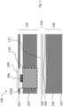
Figure 1 shows a sectional view of a dual interface laminated card according to a first embodiment; -
Figure 2 shows a sectional view of a dual interface laminated card according to a second embodiment; -
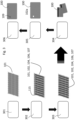
Figure 3 shows a flow diagram representing an embodiment of a method for manufacturing dual interface laminated cards according to the solution here described. - In the ensuing description, various specific details are illustrated, aimed at providing an in-depth understanding of the embodiments. The embodiments may be provided without one or more of the specific details, or with other methods, components, materials, etc. In other cases, known structures, materials, or operations are not illustrated or described in detail so that various aspects of the embodiments will not be obscured.
- Reference to "an embodiment" or "one embodiment" in the framework of the present disclosure is intended to indicate that a particular configuration, structure, or characteristic described in relation to the embodiment is comprised in at least one embodiment. Hence, phrases such as "in an embodiment" or "in one embodiment" that may be present in various points of this description do not necessarily refer to one and the same embodiment. Moreover, particular conformations, structures, or characteristics may be combined in any adequate way in one or more embodiments.
- The references used herein are provided only for convenience and hence do not define the sphere of protection or the scope of the embodiments.
- As explained previously, various embodiments of the present disclosure regard a dual interface laminated card and corresponding manufacturing method.
- In one embodiment, illustrated in
Figure 1 , alaminated card 100 comprises substantially a firstcore plastic layer 106, a secondcore plastic layer 102 arranged over said firstcore plastic layer 106, anantenna inlay 104 arranged between such first core plastic layer 106) and such firstcore plastic layer 102, amicromodule 108 arranged over said firstcore plastic layer 106. - More in detail, the
card 100 comprises a plurality of stacked layers grouped in three parts: afront layers assembly 120, aback layers assembly 140 and in between acore assembly 130 comprising theantenna inlay 104 to provide contactless communication with a reader, here not shown, such as, for instance, a contactless Point Of Sale (POS), and a bi-coated high surfaceenergy material layer 111. - Said bi-coated high surface
energy material layer 111 comprises substantially a layer of high surface energy plastic, e.g., PVC, covered on both sides with an adhesive or glue to improve adhesion, in particular an adhesive effective on high energy surfaces such as PVC, i.e. with a similar surface energy, i.e. at least in the range of high surface energy over 40 dyne/cm, to bond in particular with theantenna inlay 104, which may be made of PVC. - The
front layers assembly 120 comprises, from an inner to an external face i.e., the upper or front face of thelaminated card 100, a secondcore plastic layer 102, in which is obtained acavity 102a, which in the embodiment shown is passing through the entire thickness of the secondcore plastic layer 102, abi-adhesive material 110 fillingsuch cavity 102a. Thebi-adhesive material 110 may be a Hot Melt Adhesive (HMA). A Hot Melt or Hotmelt adhesive is usually a glue tape, heat activated double-sided film used for the embedding of chip modules into smartcard. Over the secondcore plastic layer 102, in the region of thebi-adhesive material 110 is placed amicromodule 108, over which is placed asecond overlay layer 101. An array ofelectrical contacts 109 is coupled to themicromodule 108, arranged in an opening of thesecond overlay layer 101. - The second
core plastic layer 102 can be made of a recycled plastic material, such as recycled high-density polyethylene (r-HDPE), or also recycled polyethylene terephthalate (r-PET). Such recycled materials can exhibit a low surface energy i.e., they can have a surface energy smaller up to 40 dyne/cm. - The
bi-adhesive material 110 extends from the bi-coated highsurface energy material 111, which represents the upper layer of thecore assembly 130 to themicromodule 108 above, it is configured to embed themicromodule 108 in thecavity 102a, which is obtained in the secondcore plastic layer 102 and extending vertically along the entire thickness of the secondcore plastic layer 102, thebi-adhesive material 110 also extending vertically along the entire thickness of said secondcore plastic layer 102. In particular, thebi-adhesive material 110 occupies completely thecavity 102a. - According to a preferred embodiment, the
bi-adhesive material 110 can be, for instance, a thermally activatable bi-adhesive material, i.e. a thermally activatable HMA. According to an embodiment, thebi-adhesive material 210 may be a high bond acrylic glue or a bi-component epoxy resin. Thebi-adhesive material 110 may activated, i.e. heated over its thermal activation temperature, twice, the first when it is melted inside thecavity 102a, the second when themicromodule 108 is brought in contact with thelayer 110 to promote embedding. Having thebi-adhesive material 110 in contact with the bi-coated highsurface energy material 111 allows to employ a wide range of adhesives to embed themicromodule 108 into theappropriate cavity 102a. In order to satisfy quality requirements such as, for instance, the CQM (Card Quality Management) requirements, thebi-adhesive material 110 must have a thickness of at least two times the thickness of a standard bi-adhesive material according to the state of the art. - The
micromodule 108 may be electrically programmable and capable of storing data. It can be used for various applications such as identification, access control, payment transactions, and more. - The
second overlay layer 101 is designed to protect the card from external sources of damage, and it can be personalized e.g., printed or metallized, by the card provider. Thesecond overlay layer 101 can be made of polyvinyl chloride (PVC). - The array of
electrical contacts 109 provides electrical access to themicromodule 108, to which it is electrically connected. The height of the array ofelectrical contacts 109 must satisfy electrical and mechanical requirements, specified, for instance, by the MasterCard Card Quality Management (CQM) or the ISO 7810 and ISO 7816 standards. - The above-described layers comprised in the
front layers assembly 120 i.e., the secondcore plastic layer 102 and thesecond overlay layer 101, are glued together, i.e. bonded by glue, to ensure mechanical strength and resistance to delamination according to the MasterCard CQM standard. - Thus in this embodiment the second
core plastic layer 102 is bonded through theantenna inlay 104 through thebi-coated layer 111, which on its upper surface adheres in particular to the lower surface of thebi-adhesive material 110. - In order to deal with low surface energy plastics, where the low surface energy making the operation of bonding to other materials difficult due to a scarce adhesion of such low surface energy material to other surfaces and adhesives, the solution here described, as better detailed in the following, then provides to use glues which ensure good adhesion even on low surface energy materials, in particular polyurethane heat activatable glues. A Polyurethane (or Polyurethanic) Thermoactivable glue is a heat activated, solvent based adhesive on polyurethane basis.
- Thus, the
back layers assembly 140 comprises, from the inner i.e., upper, to the external i.e., lower, face, also the external face of thecard 100, a firstcore plastic layer 106 and afirst overlay layer 107. - Similar to the second
core plastic layer 102, the firstcore plastic layer 106 can be made of a recycled plastic material, such as recycled high-density polyethylene (r-HDPE), or recycled polyethylene terephthalate (r-PET). More generally, such firstcore plastic layer 106 can be made of a low surface energy material i.e., a material with surface energy up to 40 dyne/cm. - The
first overlay layer 107 is designed to protect the card from external sources of damage, and it can be personalized e.g., printed or metallized, by the card provider. Thefirst overlay layer 107 can be made of polyvinyl chloride (PVC). - A further embodiment, illustrated in
Figure 2 , shows a dual interface laminatedcard 200 comprising a first layer of polyurethaneheat activatable glue 205 and a second layer of polyurethaneheat activatable glue 203, respectively coupled to a side facing saidantenna inlay 204 of each of a firstcore plastic layer 206 and secondcore plastic layer 202, bonding theantenna inlay 204 and the core plastic layers 202, 206 together. - Substantially, layers 201, 202, 204-207 in
Figure 2 correspond tolayers Figure 1 . - More in detail the
card 200 comprises a plurality of stacked layers grouped in three parts: afront layers assembly 220, aback layers assembly 240 and in between acore assembly 230 comprising anantenna inlay 204 to provide contactless communication with a reader such as, for instance, a contactless Point Of Sale (POS). - The
front layers assembly 220 comprises, from the inner to the external face i.e., the upper or front face of thelaminated card 200, a secondcore plastic layer 202, in which is obtained acavity 202a, which in the embodiment shown extends along a portion of the thickness of thecore plastic layer 202, abi-adhesive material 210 fillingsuch cavity 202a. Over the secondcore plastic layer 202, in the region of thebi-adhesive material 210, is placed amicromodule 208, over which is placed asecond overlay layer 201. An array ofelectrical contacts 209 is coupled to themicromodule 208, arranged in an opening of thesecond overlay layer 101. - The second
core plastic layer 202, as thelayer 102, can be made of a recycled plastic material, such as recycled high-density polyethylene (r-HDPE), or recycled polyethylene terephthalate (r-PET) . Such recycled materials can exhibit a low surface energy i.e., they can have a surface energy up to 40 Dyne/cm. - The
bi-adhesive material 210 extends vertically from the side facing thesecond overlay layer 201 to an inner portion of the secondcore plastic layer 202 and it is configured to embed themicromodule 208 in acavity 202a, obtained in the secondcore plastic layer 202 and extending vertically along the thickness of said secondcore plastic layer 202, starting from the side facing thesecond overlay layer 201 to an inner portion of the secondcore plastic layer 202. - The
micromodule 208 is electrically programmable and capable of storing data. It can be used for various applications such as identification, access control, payment transactions, and more. - The
second overlay layer 201 is designed to protect the card from external sources of damage, and it can be personalized e.g., printed or metallized, by the card provider. Thesecond overlay layer 201 can be made of polyvinyl chloride (PVC). - The array of
electrical contacts 209 provides electrical access to themicromodule 208, to which it is electrically connected. The height of the array ofelectrical contacts 209 must satisfy electrical and mechanical requirements, specified, for instance, by the MasterCard Card Quality Management (CQM) or the ISO 7810 and ISO 7816 standards. - The above-described layers comprised in the
front layers assembly 220 i.e., the firstcore plastic layer 202 and thesecond overlay layer 201, are glued together to ensure mechanical strength and resistance to delamination according to the MasterCard CQM standard. - Furthermore, the first
core plastic layer 202 is glued to thecore assembly 230, specifically to theantenna inlay 204, by means of a polyurethane heatactivatable glue layer 203, which is able to ensure a sufficiently strong bonding between said firstcore plastic layer 202 and saidantenna inlay 204. Specifically, the employ of polyurethaneheat activatable glue 203 allows to use low surface energy plastic materials, such as recycled high-density polyethylene (r-HDPE), as core plastic layers thanks to its good wetting properties on low surface energy materials. Specifically, the use of polyurethane heat activatable glue 103 allows to use low surface energy plastic materials, such as recycled high-density polyethylene (r-HDPE), as core plastic layers thanks to its good wetting properties on low surface energy materials (up to 40 dyne/cm). - The back layers
assembly 240 comprises, from the inner i.e., upper, to the external i.e., lower, face, also the external face of thecard 200, a firstcore plastic layer 206 and afirst overlay layer 207. - Similar to the first core plastic layer, the first
core plastic layer 206 can be made of a recycled plastic material, such as recycled high-density polyethylene (r-HDPE), or recycled polyethylene terephthalate. More generally, such firstcore plastic layer 206 can be made of a low surface energy material i.e., a material with surface energy up to 40 Dyne/cm. - The
first overlay layer 207 is designed to protect the card from external sources of damage, and it can be personalized e.g., printed or metallized, by the card provider. Thefirst overlay layer 207 can be made of polyvinyl chloride (PVC). - Thus, substantially, in this embodiment of
card 200, the polyurethane glue, in particular bylayer 203 is bonding also theantenna 204 to the secondplastic core layer 102, while in the embodiment ofcard 100 only the firstplastic core layer 106 is attached by the polyurethane glue, layer 105. There, thebi-coated layer 111 and thebi-adhesive material 110 instead interact to bond theassembly 120. - In view of the disclosure above, the solution here described refers to a dual interface laminated card i.e., a card with a single chip that can be used either in contact, for instance through a magnetic stripe or an EMV reader, and contactless operations, through Radio Frequency Identification (RFID) or Near Field Communication (NFC), and a corresponding method for the manufacturing thereof.
- Such dual interface laminated card, according to the
embodiments - a first core plastic layer, e.g., 106 or 206;
- a second core plastic layer, e.g.,102 or 202, arranged over the first core plastic layer, e.g., 106 or 206;
- an antenna inlay, e.g., 104, 204, arranged between the first core plastic layer, e.g., 106, 206 and second core plastic layer e.g., 106, 206;
- a micromodule, e.g., 108, arranged over said first plastic layer, e.g., 106, 206.
- According to the solution described the core plastic layers e.g., 102, 106 and 202, 206, are recycled plastic layers comprising a major percentage, in particular at least 80%, of low surface energy plastic, e.g., with surface energy up to 40 dyne/cm, such as recycled high-density polyethylene (r-HDPE), sourced from oceans; and
- said laminated card e.g., 100, 200 comprises at least a first layer of polyurethane heat activatable glue e.g., 105 in
card card 200, coupled to a side facing saidantenna inlay core plastic layer core plastic layer antenna inlay - As shown, in
Figure 2 at least one means twoplastic layer heat activatable glue Figure 1 means only the firstcore plastic layer 106 coupled by the polyurethane heat activatable glue layer 105, while attachment oflayer 102 is obtained bylayers embodiments card 100 exploiting the bi-adhesive material andcard 200 ensuring good adhesion of both the plastic layers. - Specifically, the use of polyurethane heat activatable glue enables using low surface energy plastics for manufacturing such dual interface laminated cards, thanks to the good mechanical properties, in particular resistance to delamination, yielding from the combination of such components, thereby allowing compliance to several quality standards, such as the MasterCard Card Quality Management (CQM) or the ISO 7810.
- Also, the micromodule, 108, may be bonded to said first core plastic layer, 102, by means of a
bi-adhesive material 110. - Also, the stack of the card may comprise bi-coated high
surface energy material 111 placed in between theantenna inlay 104 and the first layer of polyurethane heat activatable glue 103. - As indicated, the cavity e.g., 102a or 202a, in the second core plastic layer, 102, receives the
micromodule 108 and saidbi-adhesive material 110. The cavity may extend vertically along the entire thickness of the secondcore plastic layer 102, in particular from the side facing asecond overlay layer 101, if present, to the side facing the bi-coated highsurface energy material 111, in particular thebi-adhesive material 110 extending along all the length of thecavity 102a. Also, as depicted inFigure 2 , the micromodule, e.g. 208, and the bi-adhesive material, e.g. 210, are received in acavity 202a obtained in the firstcore plastic layer 202, said cavity, 202a, extending vertically from an upper side of the first core plastic layer, 202, i.e. the external side facing upwards opposed to the side facing theinlay layer 104, to an inner portion of the first core plastic layer, 202, such bi-adhesive material, 210, extending vertically along the entire depth of such cavity, 202a. - In embodiments, the
bi-adhesive material 110 may be a heat activatable bi-adhesive. In embodiments, the bi-adhesive material, 210, may be a high bond acrylic glue or a bi-component epoxy resin. - In an exemplary embodiment, the core plastic layers 102, 106 or 202, 206 comprise at least 80% of recycled HDPE plastic.
- As explained, although the solution refers more specifically to the inlay and core layers, the card preferably comprises also a
second overlay layer 101 and afirst overlay layer 107, wherein said overlay layers 101, 107 are printable and graphically customizable, in particular made in polyvinyl chloride (PVC). - In
Figure 3 it is shown an example of a method 300 for manufacturing dual interface laminated cards comprising steps according to the solution here described. InFigure 3 it is shown a flow diagram with blocks corresponding to the method steps, with alongside a schematic depiction of the intermediate (or final) product at that step. Thus the method 30 according to embodiments may comprise the steps of: - printing 301 the overlay layers 101, 107 (an array of
overlay 101 is shown) for customization, preferably using a dispersion of color ink and polyurethane heat activatable glue. In particular, in this step the first and second overlay layers 101, 107 are customized, then are glued on the first and second core plastic layers 106, 102 respectively, by means of glue, preferably polyurethane heat activatable glue, which is deposited on the inner faces of such first and second overlay layers 107, 101; - gathering and
pre-fixing 302 different layers (an array oflayers antenna inlay 104. In particular, the layers are arranged in a stack of layers following an order according to the embodiments shown in the foregoing. Amagnetic band 115 may also be applied on thecard 100; - assembling 303 the stack or laminate by applying pressure and heat to the layers ensemble to activate the polyurethane heat activatable glue;
- cutting 304 the stack or laminate to obtain
single cards 100; - milling 305 the cards to obtain a cavity for embedding the
micromodule 108; - embedding 306 the
micromodule 108 by means of abi-adhesive material 110. - Thus, the method 300 for manufacturing a dual interface laminated
card 100 according to the solution here described, comprises in general the steps of: - forming a stack comprising an antenna inlay, 104, between the second core plastic layer, 102, and a second core plastic layer, 106 e.g., applying
steps - embedding, 305-306, a micromodule, 108, at least in the second core plastic layer, e.g., 102,
such method comprising employing as said core plastic layers, e.g., 102, 106, low surface energy plastic material layers, preferably recycled high-density polyethylene (r-HDPE); and - depositing e.g., within the
gathering step 303, at least a first layer of polyurethane heat activatable glue, e.g., 103, or a first layer of polyurethane heat activatable glue and a second layer of polyurethane heat activatable glue, e.g., 105, on a side facing said antenna inlay, e.g., 104, of said first core plastic layer or of each of said second core plastic layer, e.g., 102, and first core plastic layer, e.g., 106, then - assembling e.g., by the
step 303, the stack, e.g., 102, 104, 106, by applying pressure and heat to it to activate the polyurethane heat activatable glue e.g., 103, 105. - Here the solution refers to a stack comprising at least the layers 102-104-106, e.g., without the overlay layers e.g., if customization is not provided or other layers with other functions. Of course, the stack may comprise such layers as well as depicted in
Figure 3 . - In embodiments, the method also includes:
- milling 305 the card to obtain a cavity, 102a, for embedding the micromodule, 108;
- embedding, 306, the micromodule, 108, by means of a bi-adhesive material, e.g., 110.
- Also, the forming step may further comprise applying a bi-coated high surface energy material, e.g., 111, between the antenna inlay, 104, which in embodiments may comprise an integrated circuit electrically connected to a plurality of metallic windings, and the
core plastic layer 102 The bi-coated high surface energy material may be preferably a high bond acrylic glue or a bi-component epoxy resin. - Also, it is provided arranging said micromodule, 108 and said
bi-adhesive material 110, in said cavity obtained in the secondcore plastic layer 102, said milling 305 the card to obtain acavity 102a for embedding themicromodule 108 comprising obtaining a cavity extending vertically along the entire thickness of the secondcore plastic layer 102, e.g., if present from the overlay layer to the side facing the bi-coated layer or theinlay layer 104, saidbi-adhesive material 110 extending vertically along the entire thickness of the secondcore plastic layer 102. - In other embodiments, arranging said
micromodule 108 and saidbi-adhesive material 110 in said cavity obtained in the firstcore plastic layer 202, includes milling so that said cavity e.g., 202a, extends vertically from an upper side of the first core plastic layer, 202, in particular from theoverlay 101 if present, to an inner portion of the first core plastic layer, 202, saidbi-adhesive material 210 extending vertically along the entire depth of such cavity. Also, as shown, an array ofelectrical contacts 109 may be embedded in a cavity extending vertically along the entire thickness of thesecond overlay layer 101, said array ofelectrical contacts 109 being electrically coupled to themicromodule 108. - It is here specified that, after the milling,
e.g. step 305, of the cavity, 102a or 202a, to improve the adhesion of themicromodule 108 is possible to apply a pretreatment, such as a Corona or Plasma pre-treatment on themilling cavity 202a. Such Corona or Plasma pre-treatment may be used also on card body materials to increase the bonding between recycled materials and other materials. - The overlay and the inlay layers are usually made mainly of high surface energy materials such as PVC o PVC/ABS.
- Also, a more comprehensive embodiment of the method here described may also include:
- printing, e.g., 301, overlay layers e.g., 101, 107, for customization, in particular using a dispersion of color ink and polyurethane heat activatable glue;
- arranging, e.g., 302, said overlay layers, e.g., 101, 107, on the external faces of said core plastic layers, 102, 106 i.e., upper face of
layer 102 and lower face oflayer 106; - performing such assembling e.g.,
step 303, the stack, in this case including also theoverlays - cutting e.g., singulating, 304 the sheet comprising the laminated stack to obtain single cards;
- performing said milling 305 the cards to obtain a cavity for embedding the
micromodule 108 comprises removing a portion of material from the front layers assembly in order to obtain thecavity 102a for embedding themicromodule 108. According to the illustrated embodiments, the cavity may extend from the top surface of thefront layers assembly 120 to thecore assembly 130, or to an inner portion of the secondcore plastic layer 102; and - embedding 306 the
micromodule 108 by means of abi-adhesive material 110, that, according to the embodiments of the solution above-described, may be a bi-adhesive specifically tailored for adherence on low surface energy materials, such as a high bond acrylic glue or a bi-component epoxy resin, or may be a heat activatable bi-adhesive. - The core plastic layers e.g., 102, 106, being low surface energy plastic material layers means that they comprise a major percentage (e.g. greater than 50%) or completely composed of low surface energy plastic material layers i.e., they include low surface energy plastic to the extent to ensure the described adhesion properties. In particular they contain at least 80% of low surface energy plastic material. Minor quantities of different plastic, which does not contribute to the adhesion properties determined by the low surface energy plastic material layers may be present.
- Thus, on the basis of the description above, the operation of the solution here described is clear, as its advantages.
- In view of the disclosure above, the solution here described advantageously provides cards with core recycled plastic layers composed by a low surface energy plastic material, such as recycled high-density polyethylene (r-HDPE) or polyethylene, sourced from oceans, such laminated card comprising at least a layer of polyurethane heat activatable glue coupled a recycled plastic layer, allowing bonding the antenna inlay and the core plastic layer or layers together ensuring a sufficiently strong bonding. Specifically, the use of polyurethane heat activatable glue enables using low surface energy plastics for manufacturing such dual interface laminated cards, thanks to the good mechanical properties, in particular resistance to delamination, yielding from the combination of such components, thereby allowing compliance to several quality standards, such as the MasterCard Card Quality Management (CQM) or the ISO 7810.
- While this invention has been described with reference to illustrative embodiments, this description is not intended to be construed in a limiting sense. Various modifications and combinations of the illustrative embodiments, as well as other embodiments of the invention, will be apparent to persons skilled in the art upon reference to the description. It is therefore intended that the appended claims encompass any such modifications or embodiments.
- As indicated the core plastic layers in the solution are recycled plastic layers, in particular from sea source, in particular coastal areas. Such plastic layers comprise a major percentage, in particular at least 80%, of recycled low surface energy plastic, which may comprise r-HDPE and/or r-PET and/or or other low surface energy recycled plastic material.
Claims (21)
- A dual interface laminated card (100; 200) comprising a stack of layers, comprising at least:- a first core plastic layer (106; 206);- a second core plastic layer (102; 202) arranged over said first core plastic layer (106; 206);- an antenna inlay (104; 204) arranged between said second core plastic layer (106; 206) and first core plastic layer (106; 206);- a micromodule (108) arranged over said second core plastic layer (106; 206);characterized in that:- said core plastic layers (102, 106; 202, 206) are recycled plastic layers comprising a major percentage, in particular at least 80%, of low surface energy plastic; and- said laminated card (100; 200) comprises at least a first layer of polyurethane heat activatable glue (105; 203, 205), coupled to a side facing said antenna inlay (104; 204) of at least one of said first core plastic layer (106; 206) and second core plastic layer (102; 202), bonding the antenna inlay (104; 204) and the at least one core plastic layer (102, 106; 202, 206) together.
- A dual interface laminated card (200) according to claim 1, wherein it comprises a first layer of polyurethane heat activatable glue (205) and a second layer of polyurethane heat activatable glue (203), respectively coupled to a side facing said antenna inlay (204) of each of said first core plastic layer (206) and second core plastic layer (202), bonding the antenna inlay (204) and the core plastic layers (202, 206) together.
- A dual interface laminated card (100) according to claim 1, wherein said card comprises only a layer of polyurethane heat activatable glue (105) coupled to a side facing said antenna inlay (104) of said first core plastic layer (106), bonding the antenna inlay (104) and the first core plastic layer (106) together.
- A dual interface laminated card (100; 200) according to claim 2 or 3 or 4, wherein said micromodule (108) is bonded to said second core plastic layer (102) by means of a bi-adhesive material (110; 210).
- A dual interface laminated card (100) according to claim 3, further comprising a bi-coated high surface energy material (111) comprising a layer of high surface energy plastic, covered on both sides with an adhesive layer, placed in between the antenna inlay (104) and the first layer of polyurethane heat activatable glue (103).
- A dual interface laminated card (100) according to claim 5 wherein said micromodule (108) and said bi-adhesive material (110) are received in a cavity (102a) obtained in the second core plastic layer (102), said cavity extending vertically along the entire thickness of the second core plastic layer (102), in particular from the side facing a second overlay layer (101) to the side facing the bi-coated high surface energy material (111), said bi-adhesive material (110) extending vertically along the entire depth of the cavity (102a).
- A dual interface laminated card (100) according to claim 6 wherein the bi-adhesive material (110) is a heat activatable bi-adhesive.
- A dual interface laminated card (200) according to claim 4, wherein the micromodule (208) and the bi-adhesive material (210) are received in a cavity (202a) obtained in the second core plastic layer (202), said cavity extending vertically from an upper side of the second core plastic layer (202) to an inner portion of the second core plastic layer (202), said bi-adhesive material (210) extending vertically along the entire depth of such cavity (202a).
- A dual interface laminated card (200) according to claim 8, wherein the bi-adhesive material (210) is a high bond acrylic glue or a bi-component epoxy resin.
- A dual interface laminated card (100) according to any of the previous claims, comprising a second overlay layer (101; 201) and a first overlay layer (107; 207), wherein said overlay layers (101; 201, 107; 207) are printable and graphically customizable, in particular made in polyvinyl chloride (PVC).
- A dual interface laminated card (100) according to any of the previous claims, wherein in said layers (102, 106; 202, 206) comprising a major percentage, in particular at least 80%, of low surface energy plastic, said low surface energy plastic is substantially recycled high-density polyethylene (r-HDPE).
- A dual interface laminated card (100) according to any of the previous claims, wherein said low surface energy plastic is a recycled plastic with a surface energy up to 40 dyne/cm, in particular up to 36 dyne/cm, in further variant embodiments below 36 dyne/cm.
- Method (300) for manufacturing a dual interface laminated card (100) comprising the steps of:- forming (302, 303) a stack comprising an antenna inlay (104) between a first core plastic layer (106; 206) and a second core plastic layer (102; 202);- embedding a micromodule (108) at least in the first core plastic layer (106; 206),said method comprising employing as said core plastic layers (102, 106; 202, 206 ) layers comprising a major percentage, in particular at least 80%, of low surface energy plastic, preferably recycled high-density polyethylene (r-HDPE); andsaid forming (302, 303) step comprising:- depositing (302) at least a layer of polyurethane heat activatable glue (105), respectively on a side facing said antenna inlay (104) of said second core plastic layer (106),assembling (304) the stack by applying pressure and heat to it to activate the polyurethane heat activatable glue (105).
- Method (300) for manufacturing a dual interface laminated card (100) according to claim 13, said forming (302, 303) step comprising:- depositing (302) a first layer of polyurethane heat activatable glue (103) and a second layer of polyurethane heat activatable glue (105), respectively on a side facing said antenna inlay (104) of each of said second core plastic layer (102) and first core plastic layer (106),
- Method (300) for manufacturing a dual interface laminated card (100) according to claim 13, said forming (302, 303) step comprising:
depositing (302) one layer of polyurethane heat activatable glue (105), respectively coupled to a side facing said antenna inlay (104) of said second core plastic layer (106), in order to bond the antenna inlay (104) and the core plastic layers (106) together. - Method (300) for manufacturing a dual interface laminated card (100) according to any of claims 13 to 15 comprising the steps of:- milling (305) the card to obtain a cavity (102a) for embedding the micromodule (108);- embedding (306) the micromodule (108) by means of a bi-adhesive material (110).
- Method (300) for manufacturing a dual interface laminated card (100) according to any of claims 13 to 15, wherein said forming (302, 303) step further comprising applying a bi-coated high surface energy material (111) between the antenna inlay (104) and the first layer of polyurethane heat activatable glue (103).
- Method (300) for manufacturing a dual interface laminated card (100) according to any of claims 15 or 16 comprising arranging said micromodule (108) and said bi-adhesive material (110) in said cavity obtained in the first core plastic layer (102), said milling (305) the card to obtain a cavity (102a) for embedding the micromodule (108) comprising obtaining a cavity extending vertically along the entire thickness of the first core plastic layer (102), said bi-adhesive material (110) extending vertically along the entire thickness of the first core plastic layer (102).
- Method (300) for manufacturing a dual interface laminated card (100) according to any of claims 15 or 16 comprising arranging said micromodule (108) and said bi-adhesive material (110) in said cavity obtained in the first core plastic layer (202), said cavity (102a) extending vertically from an upper side of the first core plastic layer (202) to an inner portion of the first core plastic layer (202), said bi-adhesive material (210) extending vertically along the entire depth of such cavity.
- Method (300) for manufacturing a dual interface laminated card (100) according to claim 19, wherein after said milling (305) of the cavity (202a) a pretreatment by Corona or Plasma pre-treatment on the cavity (202a) is performed.
- Method (300) for manufacturing a dual interface laminated card (100) according any of claims 13 to 20 comprising:- printing (301) overlay layers (101, 107) for customization, in particular using a dispersion of color ink and polyurethane heat activatable glue;- arranging (302) said overlay layers (101, 107) on the external faces of said core plastic layers (102, 106),
performing said assembling (303) the stack by applying pressure and heat to the layers ensemble to activate the polyurethane heat activatable glue;- cutting (304) the stack to obtain single cards; performing said milling (305) the cards to obtain a cavity for embedding the micromodule (108); and- embedding (306) the micromodule (108) by means of a bi-adhesive material (110).
Applications Claiming Priority (1)
| Application Number | Priority Date | Filing Date | Title |
|---|---|---|---|
| IT102023000020178A IT202300020178A1 (en) | 2023-09-29 | 2023-09-29 | LAMINATED PAPER WITH DUAL INTERFACE AND CORRESPONDING MANUFACTURING PROCEDURE OF A LAMINATED PAPER WITH DUAL INTERFACE |
Publications (1)
| Publication Number | Publication Date |
|---|---|
| EP4530060A1 true EP4530060A1 (en) | 2025-04-02 |
Family
ID=88964968
Family Applications (1)
| Application Number | Title | Priority Date | Filing Date |
|---|---|---|---|
| EP24199993.7A Withdrawn EP4530060A1 (en) | 2023-09-29 | 2024-09-12 | Dual interface laminated card and corresponding method for manufacturing a dual interface laminated card |
Country Status (3)
| Country | Link |
|---|---|
| US (1) | US12608579B2 (en) |
| EP (1) | EP4530060A1 (en) |
| IT (1) | IT202300020178A1 (en) |
Citations (2)
| Publication number | Priority date | Publication date | Assignee | Title |
|---|---|---|---|---|
| US20180323139A1 (en) * | 2015-11-05 | 2018-11-08 | Gemalto Sa | Method for manufacturing a device with integrated-circuit chip by direct deposit of conductive material |
| US20230306229A1 (en) * | 2020-06-25 | 2023-09-28 | Cpi Card Group - Colorado, Inc. | Recovered plastic cards |
Family Cites Families (5)
| Publication number | Priority date | Publication date | Assignee | Title |
|---|---|---|---|---|
| US20080150701A1 (en) * | 2006-12-26 | 2008-06-26 | Alan Randmae | Method and apparatus for forming plastics with integral RFID devices |
| JP7195350B2 (en) * | 2018-10-18 | 2022-12-23 | ポリマー キャラクタライゼーション,エセ.アー. | Deflector refractometer with extended measurement range |
| US20220126621A1 (en) * | 2020-10-26 | 2022-04-28 | Illinois Tool Works Inc. | Sheet assembly for forming one or more cards |
| IL310540A (en) * | 2021-08-16 | 2024-03-01 | Sionyx Llc | A microchannel plate enhances a figure and methods for its production |
| DE102021004951A1 (en) * | 2021-10-01 | 2023-04-06 | Giesecke+Devrient Mobile Security Gmbh | Card-shaped data carrier |
-
2023
- 2023-09-29 IT IT102023000020178A patent/IT202300020178A1/en unknown
-
2024
- 2024-09-10 US US18/830,236 patent/US12608579B2/en active Active
- 2024-09-12 EP EP24199993.7A patent/EP4530060A1/en not_active Withdrawn
Patent Citations (2)
| Publication number | Priority date | Publication date | Assignee | Title |
|---|---|---|---|---|
| US20180323139A1 (en) * | 2015-11-05 | 2018-11-08 | Gemalto Sa | Method for manufacturing a device with integrated-circuit chip by direct deposit of conductive material |
| US20230306229A1 (en) * | 2020-06-25 | 2023-09-28 | Cpi Card Group - Colorado, Inc. | Recovered plastic cards |
Also Published As
| Publication number | Publication date |
|---|---|
| IT202300020178A1 (en) | 2025-03-29 |
| US12608579B2 (en) | 2026-04-21 |
| US20250111186A1 (en) | 2025-04-03 |
Similar Documents
| Publication | Publication Date | Title |
|---|---|---|
| EP3776362B1 (en) | Portable dual-interface data carrier with metal frame | |
| US7597266B2 (en) | Method for making a smart card antenna on a thermoplastic support and resulting smartcard | |
| US6406935B2 (en) | Manufacturing process of a hybrid contact-contactless smart card with an antenna support made of fibrous material | |
| AU776169B2 (en) | Method for making a non-contact smart card with an antenna support made of fibrous material | |
| KR100998605B1 (en) | Method for manufacturing a contactless or contact / contactless hybrid chip card with improved flatness | |
| CN1787921B (en) | Method for producing book cover insert, book cover insert and book type security document | |
| US12596904B2 (en) | Recovered plastic cards | |
| US7688209B2 (en) | Radio frequency identification device resistant to humid environments and its manufacturing method | |
| US20070252705A1 (en) | Radio frequency identification device support and its manufacturing method | |
| KR20200004851A (en) | Smart card and manufacturing method with a metal layer | |
| ZA200105717B (en) | Non-contact or non-contact hybrid smart card for limiting risks of fraud. | |
| CN101535870A (en) | Method for manufacturing a smart card, smart card manufactured according to the method and LCD particularly for use with such a smart card | |
| US20230306229A1 (en) | Recovered plastic cards | |
| US8702006B2 (en) | Microcircuit card body forming a medium for two electronic labels which activate indepently based on card body face | |
| US7710276B2 (en) | Radio frequency identification device support and its manufacturing method | |
| US12608579B2 (en) | Dual interface laminated card and corresponding method for manufacturing a dual interface laminated card | |
| US20200125911A1 (en) | Interactive Core for Electronic Cards | |
| CN111126541A (en) | Structure of RFID smart card and manufacturing method thereof | |
| GB2309933A (en) | Laminated contact card manufactured by pressing contact assembly through aperture in outer layer | |
| JP2002298103A (en) | Contactless ic card and manufacturing method thereof | |
| HK1134959A1 (en) | Radio frequency identification device medium and method for making same | |
| HK1134959B (en) | Radio frequency identification device medium and method for making same |
Legal Events
| Date | Code | Title | Description |
|---|---|---|---|
| PUAI | Public reference made under article 153(3) epc to a published international application that has entered the european phase |
Free format text: ORIGINAL CODE: 0009012 |
|
| STAA | Information on the status of an ep patent application or granted ep patent |
Free format text: STATUS: THE APPLICATION HAS BEEN PUBLISHED |
|
| AK | Designated contracting states |
Kind code of ref document: A1 Designated state(s): AL AT BE BG CH CY CZ DE DK EE ES FI FR GB GR HR HU IE IS IT LI LT LU LV MC ME MK MT NL NO PL PT RO RS SE SI SK SM TR |
|
| STAA | Information on the status of an ep patent application or granted ep patent |
Free format text: STATUS: REQUEST FOR EXAMINATION WAS MADE |
|
| 17P | Request for examination filed |
Effective date: 20251001 |
|
| STAA | Information on the status of an ep patent application or granted ep patent |
Free format text: STATUS: THE APPLICATION HAS BEEN WITHDRAWN |
|
| 18W | Application withdrawn |
Effective date: 20260326 |