EP4529371A1 - Circuit connection device and rotating electrical machine device - Google Patents
Circuit connection device and rotating electrical machine device Download PDFInfo
- Publication number
- EP4529371A1 EP4529371A1 EP22942654.9A EP22942654A EP4529371A1 EP 4529371 A1 EP4529371 A1 EP 4529371A1 EP 22942654 A EP22942654 A EP 22942654A EP 4529371 A1 EP4529371 A1 EP 4529371A1
- Authority
- EP
- European Patent Office
- Prior art keywords
- terminal
- circuit board
- support member
- press
- board
- Prior art date
- Legal status (The legal status is an assumption and is not a legal conclusion. Google has not performed a legal analysis and makes no representation as to the accuracy of the status listed.)
- Pending
Links
Images









Classifications
-
- H—ELECTRICITY
- H02—GENERATION; CONVERSION OR DISTRIBUTION OF ELECTRIC POWER
- H02K—DYNAMO-ELECTRIC MACHINES
- H02K5/00—Casings; Enclosures; Supports
- H02K5/04—Casings or enclosures characterised by the shape, form or construction thereof
- H02K5/22—Auxiliary parts of casings not covered by groups H02K5/06-H02K5/20, e.g. shaped to form connection boxes or terminal boxes
- H02K5/225—Terminal boxes or connection arrangements
-
- H—ELECTRICITY
- H02—GENERATION; CONVERSION OR DISTRIBUTION OF ELECTRIC POWER
- H02K—DYNAMO-ELECTRIC MACHINES
- H02K11/00—Structural association of dynamo-electric machines with electric components or with devices for shielding, monitoring or protection
- H02K11/20—Structural association of dynamo-electric machines with electric components or with devices for shielding, monitoring or protection for measuring, monitoring, testing, protecting or switching
- H02K11/21—Devices for sensing speed or position, or actuated thereby
- H02K11/215—Magnetic effect devices, e.g. Hall-effect or magneto-resistive elements
-
- H—ELECTRICITY
- H02—GENERATION; CONVERSION OR DISTRIBUTION OF ELECTRIC POWER
- H02K—DYNAMO-ELECTRIC MACHINES
- H02K11/00—Structural association of dynamo-electric machines with electric components or with devices for shielding, monitoring or protection
- H02K11/30—Structural association with control circuits or drive circuits
- H02K11/33—Drive circuits, e.g. power electronics
-
- H—ELECTRICITY
- H02—GENERATION; CONVERSION OR DISTRIBUTION OF ELECTRIC POWER
- H02K—DYNAMO-ELECTRIC MACHINES
- H02K11/00—Structural association of dynamo-electric machines with electric components or with devices for shielding, monitoring or protection
- H02K11/40—Structural association with grounding devices
-
- H—ELECTRICITY
- H05—ELECTRIC TECHNIQUES NOT OTHERWISE PROVIDED FOR
- H05K—PRINTED CIRCUITS; CASINGS OR CONSTRUCTIONAL DETAILS OF ELECTRIC APPARATUS; MANUFACTURE OF ASSEMBLAGES OF ELECTRICAL COMPONENTS
- H05K7/00—Constructional details common to different types of electric apparatus
- H05K7/14—Mounting supporting structure in casing or on frame or rack
-
- H—ELECTRICITY
- H02—GENERATION; CONVERSION OR DISTRIBUTION OF ELECTRIC POWER
- H02K—DYNAMO-ELECTRIC MACHINES
- H02K2211/00—Specific aspects not provided for in the other groups of this subclass relating to measuring or protective devices or electric components
- H02K2211/03—Machines characterised by circuit boards, e.g. pcb
Definitions
- the present disclosure relates to a circuit connection device and a rotating electrical machine device.
- a circuit connection device including a circuit board on which electronic components are mounted and a connector including connection terminals connected to the outside is used.
- connection terminals electrical connection between the circuit board and the connector can be ensured by press-fitting the press-fit terminals into terminal holes formed in the circuit board without performing soldering or the like.
- connection terminals When the connection terminals are press-fitted into the terminal holes, a pressing force is applied to the circuit board.
- the number of the connection terminals of the connector has been increased, for example, for redundancy of the rotating electrical machine device.
- the pressing force applied to the circuit board when the connection terminals are press-fitted into the terminal holes is increased.
- Patent Document 1 there is a possibility that a distortion may occur in the circuit board due to a pressing force applied to the circuit board and the electronic components mounted on the circuit board may be damaged.
- a circuit connection device includes a connector including a connection terminal connected to an outside, a circuit board on which an electronic component is mounted and in which a terminal hole into which the connection terminal is press-fitted is formed, a board support member that supports the circuit board, and a fixing member that fixes the circuit board to the board support member, in which the circuit board includes a mounting portion on which the electronic component is mounted, and a supported portion fixed to the board support member by the fixing member and supported by the board support member, and the supported portion is disposed between the mounting portion and the terminal hole.
- a rotating electrical machine device includes a rotating electrical machine, and the circuit connection device configured to control the rotating electrical machine.
- the circuit connection device and the rotating electrical machine device capable of suppressing the distortion of the circuit board and preventing damage to the electronic component mounted on the circuit board while suppressing an increase in the number of components.
- FIG. 1 is a schematic cross-sectional view of the rotating electrical machine device 100.
- the rotating electrical machine device 100 includes a rotating electrical machine 1 that is of a multiphase winding type, and the circuit connection device 2 that controls the rotating electrical machine 1.
- the rotating electrical machine 1 mainly includes a rotating shaft 11, a rotor 12, a stator 13, a case 14, a winding 15, an annular wiring portion 16, a wiring terminal 17, and first and second bearings 18a and 18b.
- FIG. 1 is a cross-sectional view of the rotating electrical machine device 100 taken along the rotating shaft 11.
- a lower side of the drawing sheet is an output side of the rotating shaft 11
- an upper side of the drawing sheet is a non-output side of the rotating shaft 11.
- the rotating shaft 11 extends along an axis.
- the rotor 12 is fixed to the rotating shaft 11.
- a plurality of pairs of permanent magnets (not shown) are disposed on an outer peripheral surface of the rotor 12. These permanent magnets constitute field poles.
- the stator 13 is provided to surround an outer periphery of the rotor 12.
- the stator 13 is fixed to an inner surface of the case 14.
- An air gap is formed between the outer peripheral surface of the rotor 12 and an inner peripheral surface of the stator 13. The air gap is formed over the entire circumference in a circumferential direction around the axis of the rotating shaft 11.
- the case 14 accommodates the rotating shaft 11, the rotor 12, and the stator 13.
- the case 14 includes a cylindrical portion 14a and a bottom portion 14b.
- the cylindrical portion 14a covers the stator 13 from an outer peripheral side.
- the stator 13 is fixed to the cylindrical portion 14a by press-fitting.
- the bottom portion 14b covers a lower end of the cylindrical portion 14a.
- An upper end of the cylindrical portion 14a is covered with a board support member 5 of the circuit connection device 2 to be described later.
- the winding 15 is wound around the stator 13.
- the winding 15 includes a U-phase winding, a V-phase winding, and a W-phase winding.
- the annular wiring portion 16 is disposed on the non-output side (namely, the upper side in FIG. 1 ) of the rotating shaft 11 with respect to the winding 15.
- the annular wiring portion 16 is connected to an end portion of the winding 15 by TIG welding or the like.
- the wiring terminal 17 is connected to the annular wiring portion 16.
- the wiring terminal 17 extends from the annular wiring portion 16 through the board support member 5 to the non-output side of the rotating shaft 11.
- the wiring terminal 17 is electrically connected to the end portion of the winding 15 via the annular wiring portion 16.
- the wiring terminal 17 is composed of three conductors. The three conductors are respectively connected to a wiring terminal of the U-phase winding, a wiring terminal of the V-phase winding, and a wiring terminal of the W-phase winding of the winding 15.
- the first bearing 18a is provided at an end portion on the non-output side of the rotating shaft 11.
- the first bearing 18a is fixed to the board support member 5.
- the second bearing 18b is provided at an end portion on the output side of the rotating shaft 11.
- the second bearing 18b is fixed to the bottom portion 14b.
- the first bearing 18a and the second bearing 18b rotatably support the rotating shaft 11.
- a sensor rotor 19 is fixed to an end surface on the non-output side of the rotating shaft 11.
- the sensor rotor 19 rotates together with the rotating shaft 11.
- the sensor rotor 19 includes a pair of, or a plurality of pairs of permanent magnets.
- the circuit connection device 2 is a control unit that controls a current flowing through the winding 15 of the rotating electrical machine 1.
- the circuit connection device 2 includes a circuit board 3, a connector 4, the board support member 5, first fastening members 6 (fixing member), a second fastening member 7, and a cover 20.
- the cover 20 covers the circuit board 3 and the board support member 5.
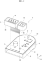
- FIG. 2 is a perspective view of the circuit connection device 2, and is a view showing a state in which the cover 20 is removed.
- the circuit board 3 is a printed wiring board. As shown in FIG. 1 , the circuit board 3 has a first surface 3a and a second surface 3b.
- FIG. 3A is a perspective view of the circuit board 3 when viewed from the first surface 3a side
- FIG. 3B is a perspective view of the circuit board 3 when viewed from the second surface 3b side.
- first direction D1 one direction in a plane along the first surface 3a
- second direction D2 a direction orthogonal to the first direction D1 in the plane
- third direction D3 a direction orthogonal to the first direction D1 and the second direction D2
- the third direction D3 is a thickness direction of the circuit board 3.
- a side on which the circuit board 3 is located is referred to as an upper side
- a side on which the board support member 5 is located is referred to as a lower side.
- the first surface 3a is a surface on the upper side of the circuit board 3
- the second surface 3b is a surface on the lower side of the circuit board 3.
- the circuit board 3 includes a power circuit that drives the rotating electrical machine 1, a control circuit that controls the driving of the rotating electrical machine 1, a signal circuit to which signals from a sensor and the like are input, a noise filter circuit that removes noise components included in power supply and signals, and the like.
- Various electronic components 31 constituting the above-described circuits are mounted on the circuit board 3.
- the electronic components 31 are mounted on the first surface 3a and the second surface 3b of the circuit board 3.
- the control circuit includes a rotation sensor 31A as the electronic component 31.
- the rotation sensor 31A is mounted on the second surface 3b of the circuit board 3.
- the rotation sensor 31A is a magnetic sensor. As shown in FIG. 1 , the rotation sensor 31A is disposed coaxially with the sensor rotor 19. The sensor rotor 19 and the rotation sensor 31A face each other with a gap interposed therebetween.
- the rotation sensor 31A detects a change in a magnetic field from the permanent magnets of the sensor rotor 19 rotating together with the rotating shaft 11, and converts the change into an electric signal.
- the sensor rotor 19 and the rotation sensor 31A detect the rotation state of the rotating shaft 11.
- a resolver, a hall sensor, an optical sensor, or the like may be used as the rotation sensor 31A.
- a plurality of terminal holes 32 are formed in the circuit board 3.
- the plurality of terminal holes 32 are disposed side by side at equal intervals in the first direction D1.
- the intervals between the plurality of terminal holes 32 may not be equal intervals.
- the plurality of terminal holes 32 are disposed at an end portion on one side of the circuit board 3 in the second direction D2.
- the terminal holes 32 penetrate the circuit board 3 in the third direction D3.
- the terminal holes 32 may be distributed and disposed at a plurality of locations.
- a plurality of press-fit terminals 44 of the connector 4 to be described later are press-fitted into the plurality of terminal holes 32.
- Conductive layers (electrical connection patterns) (not shown) to be connected to the press-fit terminals 44 are formed on inner surfaces of the terminal holes 32.
- the circuit board 3 includes a mounting portion R11, a terminal-side supported portion R12 (supported portion), and a winding-side supported portion R13.
- the electronic components 31 are mounted on the mounting portion R11.
- the mounting portion R11 is disposed between the terminal-side supported portion R12 and the winding-side supported portion R13.
- the terminal-side supported portion R12 is disposed between the mounting portion R11 and the terminal holes 32.
- First fastening holes 33 into which the first fastening members 6 are mounted are formed in the terminal-side supported portion R12.
- the first fastening holes 33 penetrate the circuit board 3 in the third direction D3.
- two first fastening holes 33 are formed side by side in the first direction D1.
- the number of the first fastening holes 33 may be 1 or 3 or more.
- the second surface 3b of the circuit board 3 is in contact with a support surface 5a of the board support member 5.
- the terminal-side supported portion R12 is supported by the board support member 5.
- the terminal-side supported portion R12 is fixed to the board support member 5 by the first fastening members 6.
- the winding-side supported portion R13 is disposed on a side opposite to the terminal-side supported portion R12 with the mounting portion R11 interposed therebetween.
- the winding-side supported portion R13 is disposed at an end portion on the other side of the circuit board 3 in the second direction D2.
- the winding-side supported portion R13 may be disposed inside the mounting portion R11.
- a second fastening hole 34 into which the second fastening member 7 is mounted is formed in the winding-side supported portion R13.
- the second fastening hole 34 penetrates the circuit board 3 in the third direction D3. In the shown example, one second fastening hole 34 is formed.
- the number of the second fastening holes 34 may be 2 or more.
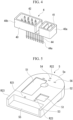
- FIG. 4 is a perspective view of the connector 4.
- the connector 4 supplies electric power from an external power supply to the circuit board 3.
- the connector 4 supplies various signals from an external control device or the like to the circuit board 3.
- the connector 4 includes a main body portion 40, power supply terminals 41, signal terminals 42, and the plurality of press-fit terminals 44 (connection terminals).
- the noise suppression component 31B can be connected to the GND via the board support member 5 and the first fastening member 6.
- the GND pattern 71 may be formed to extend to the second surface 3b of the circuit board 3 in the terminal-side supported portion R12. In this case, the GND pattern 71 is directly connected to the board support member 5.
- the X capacitor and the Y capacitor of the noise suppression component 31B are connected to the GND via the GND pattern 71 and the board support member 5.
- circuit connection device 2E according to a sixth embodiment will be described with reference to FIGS. 19A and 19B .
- Components having the same functions and actions as those in the first to fifth embodiments are denoted by the same reference signs, and a description thereof will be omitted.
- the connector 4 includes a recessed connector component 81 instead of the plurality of press-fit terminals 44.
- the recessed connector component 81 includes a plurality of connection terminals 81a disposed side by side in the first direction D1, and a holding member 81b that holds the plurality of connection terminals 81a.
- the holding member 81b includes a recessed portion, and the plurality of connection terminals 81a are disposed inside the recessed portion.
- the first fastening member 6 and the second fastening member 7 are not limited to screws as long as they are able to fix the circuit board 3 to the board support member 5.
- the board support member 5 may be integrally formed with the case 14 of the rotating electrical machine 1.
- the plurality of terminal holes 32 may be disposed at an end portion on one side in the first direction D1.
- the mounting portion R11 may be disposed at an end portion on the other side in the first direction D1
- the terminal-side supported portion R12 may be disposed to be interposed between the mounting portion R11 and the terminal holes 32 in the first direction D1.
- the plurality of terminal holes 32 may be disposed in combination at the end portion on the one side in the first direction D1 and the end portion on the one side in the second direction D2.
Landscapes
- Engineering & Computer Science (AREA)
- Power Engineering (AREA)
- Microelectronics & Electronic Packaging (AREA)
- Coupling Device And Connection With Printed Circuit (AREA)
Abstract
Description
- The present disclosure relates to a circuit connection device and a rotating electrical machine device.
- In the related art, as a control unit for a rotating electrical machine device, a circuit connection device including a circuit board on which electronic components are mounted and a connector including connection terminals connected to the outside is used. For example, when press-fit terminals are used as the connection terminals, electrical connection between the circuit board and the connector can be ensured by press-fitting the press-fit terminals into terminal holes formed in the circuit board without performing soldering or the like.
- [Patent Document 1]
PCT International Publication No. WO 2021/161947 - When the connection terminals are press-fitted into the terminal holes, a pressing force is applied to the circuit board. In recent years, the number of the connection terminals of the connector has been increased, for example, for redundancy of the rotating electrical machine device. In this case, the pressing force applied to the circuit board when the connection terminals are press-fitted into the terminal holes is increased. In the structure of
Patent Document 1, there is a possibility that a distortion may occur in the circuit board due to a pressing force applied to the circuit board and the electronic components mounted on the circuit board may be damaged. -
Patent Document 1 also discloses a structure in which a control unit includes a parent board on which the electronic components are mounted and a child board to which the connection terminals are connected. However, in this case, the number of components of the rotating electrical machine device is increased. - The present disclosure has been made to solve the above-described problems, and an object of the present disclosure is to provide a circuit connection device and a rotating electrical machine device capable of suppressing the distortion of a circuit board and preventing damage to an electronic component mounted on the circuit board while suppressing an increase in the number of components.
- A circuit connection device according to the present disclosure includes a connector including a connection terminal connected to an outside, a circuit board on which an electronic component is mounted and in which a terminal hole into which the connection terminal is press-fitted is formed, a board support member that supports the circuit board, and a fixing member that fixes the circuit board to the board support member, in which the circuit board includes a mounting portion on which the electronic component is mounted, and a supported portion fixed to the board support member by the fixing member and supported by the board support member, and the supported portion is disposed between the mounting portion and the terminal hole.
- A rotating electrical machine device according to the present disclosure includes a rotating electrical machine, and the circuit connection device configured to control the rotating electrical machine.
- According to the present disclosure, it is possible to provide the circuit connection device and the rotating electrical machine device capable of suppressing the distortion of the circuit board and preventing damage to the electronic component mounted on the circuit board while suppressing an increase in the number of components.
-
-
FIG. 1 is a schematic cross-sectional view of a rotating electrical machine device according to a first embodiment. -
FIG. 2 is a perspective view of a circuit connection device according to the first embodiment. -
FIG. 3A is a perspective view of a circuit board according to the first embodiment. -
FIG. 3B is a perspective view of the circuit board according to the first embodiment. -
FIG. 4 is a perspective view of a connector according to the first embodiment. -
FIG. 5 is a perspective view of a board support member according to the first embodiment. -
FIG. 6 is a perspective view of the circuit board and the board support member according to the first embodiment. -
FIG. 7A is a view showing a schematic configuration of the circuit connection device according to the first embodiment. -
FIG. 7B is a view showing the schematic configuration of the circuit connection device according to the first embodiment. -
FIG. 8A is a view showing a schematic configuration of a circuit connection device according to a modification example of the first embodiment. -
FIG. 8B is a view showing the schematic configuration of the circuit connection device according to the modification example of the first embodiment. -
FIG. 9A is a view showing a schematic configuration of a circuit connection device according to another modification example of the first embodiment. -
FIG. 9B is a view showing the schematic configuration of the circuit connection device according to the other modification example of the first embodiment. -
FIG. 10 is a perspective view of a circuit connection device according to a second embodiment. -
FIG. 11 is a perspective view of a circuit board and a board support member according to the second embodiment. -
FIG. 12A is a view showing a schematic configuration of the circuit connection device according to the second embodiment. -
FIG. 12B is a view showing the schematic configuration of the circuit connection device according to the second embodiment. -
FIG. 13A is a view showing a schematic configuration of a circuit connection device according to a modification example of the second embodiment. -
FIG. 13B is a view showing the schematic configuration of the circuit connection device according to the modification example of the second embodiment. -
FIG. 14A is a view showing a schematic configuration of a circuit connection device according to a third embodiment. -
FIG. 14B is a view showing the schematic configuration of the circuit connection device according to the third embodiment. -
FIG. 15 is a view showing a schematic configuration of a circuit connection device according to a modification example of the third embodiment. -
FIG. 16A is a view showing a schematic configuration of a circuit connection device according to a fourth embodiment. -
FIG. 16B is a view showing the schematic configuration of the circuit connection device according to the fourth embodiment. -
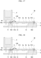
FIG. 17 is a view showing a schematic configuration of a circuit connection device according to a fifth embodiment. -
FIG. 18 is a view showing a schematic configuration of a circuit connection device according to a modification example of the fifth embodiment. -
FIG. 19A is a view showing a schematic configuration of a circuit connection device according to a sixth embodiment. -
FIG. 19B is a view showing the schematic configuration of the circuit connection device according to the sixth embodiment. -
FIG. 20A is a view showing a schematic configuration of a circuit connection device according to a comparative example of the first embodiment. -
FIG. 20B is a view showing the schematic configuration of the circuit connection device according to the comparative example of the first embodiment. - Hereinafter, a
circuit connection device 2 and a rotatingelectrical machine device 100 according to a first embodiment will be described with reference to the drawings. -
FIG. 1 is a schematic cross-sectional view of the rotatingelectrical machine device 100. The rotatingelectrical machine device 100 includes a rotatingelectrical machine 1 that is of a multiphase winding type, and thecircuit connection device 2 that controls the rotatingelectrical machine 1. - The rotating
electrical machine 1 mainly includes arotating shaft 11, arotor 12, astator 13, acase 14, a winding 15, anannular wiring portion 16, awiring terminal 17, and first andsecond bearings -
FIG. 1 is a cross-sectional view of the rotatingelectrical machine device 100 taken along the rotatingshaft 11. InFIG. 1 , a lower side of the drawing sheet is an output side of therotating shaft 11, and an upper side of the drawing sheet is a non-output side of therotating shaft 11. - The rotating
shaft 11 extends along an axis. Therotor 12 is fixed to therotating shaft 11. A plurality of pairs of permanent magnets (not shown) are disposed on an outer peripheral surface of therotor 12. These permanent magnets constitute field poles. - The
stator 13 is provided to surround an outer periphery of therotor 12. Thestator 13 is fixed to an inner surface of thecase 14. An air gap is formed between the outer peripheral surface of therotor 12 and an inner peripheral surface of thestator 13. The air gap is formed over the entire circumference in a circumferential direction around the axis of therotating shaft 11. - The
case 14 accommodates therotating shaft 11, therotor 12, and thestator 13. Thecase 14 includes acylindrical portion 14a and abottom portion 14b. Thecylindrical portion 14a covers thestator 13 from an outer peripheral side. Thestator 13 is fixed to thecylindrical portion 14a by press-fitting. Thebottom portion 14b covers a lower end of thecylindrical portion 14a. An upper end of thecylindrical portion 14a is covered with aboard support member 5 of thecircuit connection device 2 to be described later. - The winding 15 is wound around the
stator 13. The winding 15 includes a U-phase winding, a V-phase winding, and a W-phase winding. - The
annular wiring portion 16 is disposed on the non-output side (namely, the upper side inFIG. 1 ) of therotating shaft 11 with respect to the winding 15. Theannular wiring portion 16 is connected to an end portion of the winding 15 by TIG welding or the like. - The
wiring terminal 17 is connected to theannular wiring portion 16. Thewiring terminal 17 extends from theannular wiring portion 16 through theboard support member 5 to the non-output side of therotating shaft 11. Thewiring terminal 17 is electrically connected to the end portion of the winding 15 via theannular wiring portion 16. Thewiring terminal 17 is composed of three conductors. The three conductors are respectively connected to a wiring terminal of the U-phase winding, a wiring terminal of the V-phase winding, and a wiring terminal of the W-phase winding of the winding 15. - The
first bearing 18a is provided at an end portion on the non-output side of therotating shaft 11. Thefirst bearing 18a is fixed to theboard support member 5. Thesecond bearing 18b is provided at an end portion on the output side of therotating shaft 11. Thesecond bearing 18b is fixed to thebottom portion 14b. Thefirst bearing 18a and thesecond bearing 18b rotatably support the rotatingshaft 11. - A sensor rotor 19 is fixed to an end surface on the non-output side of the
rotating shaft 11. The sensor rotor 19 rotates together with the rotatingshaft 11. The sensor rotor 19 includes a pair of, or a plurality of pairs of permanent magnets. - The
circuit connection device 2 is a control unit that controls a current flowing through the winding 15 of the rotatingelectrical machine 1. Thecircuit connection device 2 includes acircuit board 3, aconnector 4, theboard support member 5, first fastening members 6 (fixing member), asecond fastening member 7, and acover 20. Thecover 20 covers thecircuit board 3 and theboard support member 5.FIG. 2 is a perspective view of thecircuit connection device 2, and is a view showing a state in which thecover 20 is removed. - The
circuit board 3 is a printed wiring board. As shown inFIG. 1 , thecircuit board 3 has afirst surface 3a and asecond surface 3b.FIG. 3A is a perspective view of thecircuit board 3 when viewed from thefirst surface 3a side, andFIG. 3B is a perspective view of thecircuit board 3 when viewed from thesecond surface 3b side. - Hereinafter, as shown in
FIG. 2 , one direction in a plane along thefirst surface 3a is referred to as a first direction D1, and a direction orthogonal to the first direction D1 in the plane is referred to as a second direction D2. In addition, a direction orthogonal to the first direction D1 and the second direction D2 is referred to as a third direction D3. The third direction D3 is a thickness direction of thecircuit board 3. In the third direction D3, a side on which thecircuit board 3 is located is referred to as an upper side, and a side on which theboard support member 5 is located is referred to as a lower side. Thefirst surface 3a is a surface on the upper side of thecircuit board 3, and thesecond surface 3b is a surface on the lower side of thecircuit board 3. - The
circuit board 3 includes a power circuit that drives the rotatingelectrical machine 1, a control circuit that controls the driving of the rotatingelectrical machine 1, a signal circuit to which signals from a sensor and the like are input, a noise filter circuit that removes noise components included in power supply and signals, and the like. Variouselectronic components 31 constituting the above-described circuits are mounted on thecircuit board 3. Theelectronic components 31 are mounted on thefirst surface 3a and thesecond surface 3b of thecircuit board 3. - The control circuit includes a
rotation sensor 31A as theelectronic component 31. Therotation sensor 31A is mounted on thesecond surface 3b of thecircuit board 3. Therotation sensor 31A is a magnetic sensor. As shown inFIG. 1 , therotation sensor 31A is disposed coaxially with the sensor rotor 19. The sensor rotor 19 and therotation sensor 31A face each other with a gap interposed therebetween. Therotation sensor 31A detects a change in a magnetic field from the permanent magnets of the sensor rotor 19 rotating together with the rotatingshaft 11, and converts the change into an electric signal. The sensor rotor 19 and therotation sensor 31A detect the rotation state of therotating shaft 11. A resolver, a hall sensor, an optical sensor, or the like may be used as therotation sensor 31A. - A plurality of
terminal holes 32 are formed in thecircuit board 3. The plurality ofterminal holes 32 are disposed side by side at equal intervals in the first direction D1. The intervals between the plurality ofterminal holes 32 may not be equal intervals. - The plurality of
terminal holes 32 are disposed at an end portion on one side of thecircuit board 3 in the second direction D2. The terminal holes 32 penetrate thecircuit board 3 in the third direction D3. The terminal holes 32 may be distributed and disposed at a plurality of locations. - A plurality of press-
fit terminals 44 of theconnector 4 to be described later are press-fitted into the plurality of terminal holes 32. Conductive layers (electrical connection patterns) (not shown) to be connected to the press-fit terminals 44 are formed on inner surfaces of the terminal holes 32. - As shown in
FIGS. 3A and 3B , thecircuit board 3 includes a mounting portion R11, a terminal-side supported portion R12 (supported portion), and a winding-side supported portion R13. - The
electronic components 31 are mounted on the mounting portion R11. The mounting portion R11 is disposed between the terminal-side supported portion R12 and the winding-side supported portion R13. - The terminal-side supported portion R12 is disposed between the mounting portion R11 and the terminal holes 32. First fastening holes 33 into which the
first fastening members 6 are mounted are formed in the terminal-side supported portion R12. The first fastening holes 33 penetrate thecircuit board 3 in the third direction D3. In the shown example, two first fastening holes 33 are formed side by side in the first direction D1. The number of the first fastening holes 33 may be 1 or 3 or more. - In the terminal-side supported portion R12, the
second surface 3b of thecircuit board 3 is in contact with asupport surface 5a of theboard support member 5. The terminal-side supported portion R12 is supported by theboard support member 5. The terminal-side supported portion R12 is fixed to theboard support member 5 by thefirst fastening members 6. - The winding-side supported portion R13 is disposed on a side opposite to the terminal-side supported portion R12 with the mounting portion R11 interposed therebetween. The winding-side supported portion R13 is disposed at an end portion on the other side of the
circuit board 3 in the second direction D2. The winding-side supported portion R13 may be disposed inside the mounting portion R11. Asecond fastening hole 34 into which thesecond fastening member 7 is mounted is formed in the winding-side supported portion R13. Thesecond fastening hole 34 penetrates thecircuit board 3 in the third direction D3. In the shown example, onesecond fastening hole 34 is formed. The number of the second fastening holes 34 may be 2 or more. - In the winding-side supported portion R13, the
second surface 3b of thecircuit board 3 is in contact with thesupport surface 5a of theboard support member 5. The winding-side supported portion R13 is supported by theboard support member 5. The winding-side supported portion R13 is fixed to theboard support member 5 by thesecond fastening member 7. - A plurality (three in the present embodiment) of winding through-
holes 35 are formed in thecircuit board 3. The winding through-holes 35 penetrates thecircuit board 3 in the third direction D3. The three conductors of thewiring terminal 17 are respectively inserted through the winding through-holes 35. An end portion of thewiring terminal 17 is connected to thecircuit board 3 by soldering or the like. -
FIG. 4 is a perspective view of theconnector 4. Theconnector 4 supplies electric power from an external power supply to thecircuit board 3. Theconnector 4 supplies various signals from an external control device or the like to thecircuit board 3. As shown inFIG. 4 , theconnector 4 includes amain body portion 40,power supply terminals 41,signal terminals 42, and the plurality of press-fit terminals 44 (connection terminals). - The
main body portion 40 is made of resin. For example, the material of themain body portion 40 is polybutylene terephthalate (PBT) or polyphenylene sulfide (PPS). Themain body portion 40 includes a power supply-side housing 40a that accommodates thepower supply terminals 41 inside, and a signal-side housing 40b that accommodates thesignal terminals 42 inside. In the present embodiment, the power supply-side housing 40a and the signal-side housing 40b are separate containers; however, the power supply-side housing 40a and the signal-side housing 40b may be formed of a single container. In addition, the power supply-side housing 40a and the signal-side housing 40b may be formed of three or more containers. Namely, thepower supply terminals 41 and thesignal terminals 42 may be accommodated in a single container or may be separately accommodated in three or more containers. - The
power supply terminals 41 are connected to the external power supply. Thesignal terminals 42 are connected to the external control device or the like. In the present embodiment, thepower supply terminals 41 and thesignal terminals 42 have different shapes; however, terminals having the same shape may be used as thepower supply terminals 41 and thesignal terminals 42. Terminals having three or more types of shapes may be used as thepower supply terminals 41 and thesignal terminals 42. - The plurality of press-
fit terminals 44 are provided to correspond to thepower supply terminals 41 and thesignal terminals 42. A plurality of the press-fit terminals 44 may be provided for onepower supply terminal 41. The press-fit terminal 44 is connected to the correspondingpower supply terminal 41 or thecorresponding signal terminal 42. The press-fit terminals 44 extend in the third direction D3. The press-fit terminals 44 extend in a direction opposite to an extending direction of thepower supply terminals 41 and thesignal terminals 42. The plurality of press-fit terminals 44 are disposed side by side at equal intervals in the first direction D1. The press-fit terminals 44 may extend in a direction intersecting the extending direction of thepower supply terminals 41 and the signal terminals 42 (for example, a direction orthogonal to the extending direction of thepower supply terminals 41 and the signal terminals 42). The plurality of press-fit terminals 44 may be distributed and disposed at a plurality of locations. - Each of the press-
fit terminals 44 is formed in an elongated plate shape as a whole. A press-fit portion 44a is formed at a distal end portion of the press-fit terminal 44. A width (maximum width) of the press-fit portion 44a is larger than a diameter of theterminal hole 32. A hole is formed in the press-fit portion 44a, and accordingly, the press-fit portion 44a can be elastically deformed. A recessed portion that allows the press-fit portion 44a to be elastically deformed may be formed in the press-fit portion 44a. - The press-
fit terminals 44 are press-fitted into the terminal holes 32. At this time, the press-fit terminals 44 come into contact with the conductive layers formed on the inner surfaces of the terminal holes 32, and are electrically connected thereto. Accordingly, theconnector 4 is electrically connected to thecircuit board 3. By using the press-fit terminals 44, thecircuit board 3 and theconnector 4 can be electrically connected to each other without performing soldering or the like. Therefore, the manufacturing of thecircuit connection device 2 is facilitated, and the manufacturing time can be shortened. - As shown in
FIG. 1 , theboard support member 5 is provided between thestator 13 and thecircuit board 3. Theboard support member 5 is fixed to thecase 14. Theboard support member 5 covers thestator 13 from above. Theboard support member 5 serves as a lid that closes the inside of the rotatingelectrical machine 1. - The
circuit board 3 is attached to theboard support member 5. Theboard support member 5 has thesupport surface 5a that supports thecircuit board 3. Thesupport surface 5a is a surface on the upper side of theboard support member 5. Theboard support member 5 is made of, for example, metal. For example, the material of theboard support member 5 is aluminum or an aluminum alloy such as ADC12. Theboard support member 5 may be made of resin such as polybutylene terephthalate (PBT) or polyphenylene sulfide (PPS). -
FIG. 5 is a perspective view of theboard support member 5. - As shown in
FIG. 5 , first accommodating recessedportions 51 that accommodate theelectronic components 31 mounted on thesecond surface 3b of thecircuit board 3 are provided on thesupport surface 5a of theboard support member 5. The first accommodating recessedportions 51 are provided at positions corresponding to the mounting portion R11. In the shown example, two first accommodating recessedportions 51 are formed. The number of the first accommodating recessedportions 51 may be 1 or 3 or more. - A rotating shaft through-
hole 52 is formed in theboard support member 5. The rotating shaft through-hole 52 penetrates theboard support member 5 in the third direction D3. As shown inFIG. 1 , the end portion on the non-output side of therotating shaft 11 is inserted into the rotating shaft through-hole 52. - The
board support member 5 includes a terminal-side supporting portion R21 (supporting portion) and a winding-side supporting portion R22. In the present embodiment, thesupport surface 5a of theboard support member 5 is configured as a single surface that extends continuously from the terminal-side supporting portion R21 to the winding-side supporting portion R22 over the entire region of theboard support member 5. However, thesupport surface 5a may be divided into a plurality of surfaces depending on the shapes of the first accommodating recessed portions 51 (namely, depending on the disposition of theelectronic components 31 mounted on thesecond surface 3b of the circuit board 3) or the like. - The terminal-side supporting portion R21 is provided at a position corresponding to the terminal-side supported portion R12 of the
circuit board 3. The terminal-side supporting portion R21 supports the terminal-side supported portion R12 from below. - Third fastening holes 53 into which the
first fastening members 6 are mounted are formed in the terminal-side supporting portion R21. The third fastening holes 53 are formed at positions corresponding to the first fastening holes 33. In the shown example, two third fastening holes 53 are formed. The number of the third fastening holes 53 may be 1 or 3 or more. - The winding-side supporting portion R22 is provided at a position corresponding to the winding-side supported portion R13 of the
circuit board 3. The winding-side supporting portion R22 supports the winding-side supported portion R13 from below. - A
fourth fastening hole 54 into which thesecond fastening member 7 is mounted is formed in the winding-side supporting portion R22. Thefourth fastening hole 54 is formed at a position corresponding to thesecond fastening hole 34. In the shown example, onefourth fastening hole 54 is formed. The number of the fourth fastening holes 54 may be 2 or more. - A second accommodating recessed
portion 55 is provided on thesupport surface 5a of theboard support member 5. The second accommodating recessedportion 55 is provided at a position corresponding to the terminal holes 32. The distal end portions of the press-fit terminals 44 press-fitted into the terminal holes 32 are accommodated in the second accommodating recessedportion 55. The second accommodating recessedportion 55 is partitioned by the terminal-side supporting portion R21 and a pair of side portions R23 extending from both ends of the terminal-side supporting portion R21 in the first direction D1 toward the one side in the second direction D2. The second accommodating recessedportion 55 is open toward the one side in the second direction D2. The pair of side portions R23 may be omitted. - A plurality (three in the present embodiment) of winding through-
holes 56 are formed in theboard support member 5. The winding through-holes 56 penetrate theboard support member 5 in the third direction D3. The three conductors of thewiring terminal 17 are respectively inserted through the winding through-holes 56. - The
first fastening members 6 are, for example, screws. Thefirst fastening members 6 are made of metal. For example, the material of thefirst fastening members 6 is iron or stainless steel. Thefirst fastening members 6 may be made of resin such as polyphenylene sulfide (PPS). Thefirst fastening members 6 are mounted into the first fastening holes 33 and the third fastening holes 53 from thefirst surface 3a side of thecircuit board 3. Thefirst fastening members 6 fix thecircuit board 3 to theboard support member 5 in a state in which thecircuit board 3 is pressed toward theboard support member 5. - The
second fastening member 7 is, for example, a screw. Thesecond fastening member 7 may be made of resin. Thesecond fastening member 7 may be made of metal. Thesecond fastening member 7 is mounted into thesecond fastening hole 34 and thefourth fastening hole 54 from thefirst surface 3a side of thecircuit board 3. Thesecond fastening member 7 fixes thecircuit board 3 to theboard support member 5 in a state in which thecircuit board 3 is pressed toward theboard support member 5. - Next, a method for manufacturing the
circuit connection device 2 according to the first embodiment will be described with reference toFIGS. 2 ,6 ,7A, and 7B . - As shown in
FIG. 6 , first, thecircuit board 3 is attached to theboard support member 5. At this time, thesupport surface 5a of theboard support member 5 and thesecond surface 3b of thecircuit board 3 face each other. The terminal-side supported portion R12 of thecircuit board 3 is placed on the terminal-side supporting portion R21 of theboard support member 5. The winding-side supported portion R13 of thecircuit board 3 is placed on the winding-side supporting portion R22 of theboard support member 5. Theelectronic components 31 mounted on thesecond surface 3b of thecircuit board 3 are accommodated in the first accommodating recessedportions 51. Thecircuit board 3 and theboard support member 5 are fastened to each other by mounting thefirst fastening members 6 into the first fastening holes 33 and the third fastening holes 53 and mounting thesecond fastening member 7 into thesecond fastening hole 34 and thefourth fastening hole 54. - Next, the
connector 4 is attached to thecircuit board 3. As shown inFIG. 7A , theconnector 4 is disposed on thefirst surface 3a side of thecircuit board 3. Theconnector 4 is disposed such that the terminal-side supported portion R12 (namely, the first fastening members 6) and theconnector 4 overlap each other when viewed in the third direction D3. As shown inFIG. 7B , theconnector 4 is pressed toward thecircuit board 3, and the press-fit terminals 44 are press-fitted into the terminal holes 32. Namely, in the present embodiment, the press-fit terminals 44 are press-fitted into the terminal holes 32 toward the lower side. A direction in which the press-fit terminals 44 are press-fitted is substantially the same as the third direction D3. In the shown example, when the press-fit terminals 44 are press-fitted into the terminal holes 32, thecircuit board 3 and theconnector 4 are disposed to be separated from each other. However, thecircuit board 3 and theconnector 4 may be disposed in proximity to or in contact with each other as long as theconnector 4 may not interfere with thefirst fastening members 6. - Here, when the press-
fit terminals 44 are press-fitted into the terminal holes 32, a pressing force is applied to thecircuit board 3. In the present embodiment, the terminal-side supported portion R12 supported by the terminal-side supporting portion R21 is provided between the mounting portion R11 and the terminal holes 32. Since the pressing force applied to thecircuit board 3 can be received by the terminal-side supported portion R12, the pressing force can be prevented from being directly transmitted to the mounting portion R11, and the distortion of the mounting portion R11 can be suppressed. - As described above, the
circuit connection device 2 according to the present embodiment includes theconnector 4 including the press-fit terminal 44 connected to the outside, thecircuit board 3 on which theelectronic component 31 is mounted and in which theterminal hole 32 into which the press-fit terminal 44 is press-fitted is formed, theboard support member 5 that supports thecircuit board 3, and thefirst fastening member 6 that fixes thecircuit board 3 to theboard support member 5. Thecircuit board 3 includes the mounting portion R11 on which theelectronic component 31 is mounted, and the terminal-side supported portion R12 fixed to theboard support member 5 by thefirst fastening member 6 and supported by theboard support member 5. The terminal-side supported portion R12 is disposed between the mounting portion R11 and theterminal hole 32. - The
circuit board 3 includes the terminal-side supported portion R12 that is disposed between the mounting portion R11 on which theelectronic component 31 is mounted and theterminal hole 32, and that is supported by theboard support member 5. Therefore, a pressing force applied to thecircuit board 3 when the press-fit terminal 44 is press-fitted into theterminal hole 32 can be received by the terminal-side supported portion R12, and the pressing force can be prevented from being directly transmitted to the mounting portion R11. Therefore, the distortion of thecircuit board 3 can be suppressed, and theelectronic component 31 mounted on the mounting portion R11 can be prevented from being damaged. In addition, theelectronic component 31 is mounted on thecircuit board 3, and theterminal hole 32 into which the press-fit terminal 44 is press-fitted is formed in thecircuit board 3. Therefore, compared to a case where a parent board on which an electronic component is mounted and a child board to which a press-fit terminal is connected are separately provided, an increase in the number of components of thecircuit connection device 2 can be suppressed. As described above, according to thecircuit connection device 2 of the present embodiment, it is possible to suppress the distortion of thecircuit board 3 and prevent damage to theelectronic component 31 mounted on thecircuit board 3 while suppressing an increase in the number of components. - In addition, compared to a case where the terminal-side supported portion R12 is not provided, the
electronic component 31 can be mounted at a position closer to theterminal hole 32, so that the mounting region of theelectronic component 31 is expanded. Since theelectronic component 31 can be efficiently mounted on thecircuit board 3, thecircuit board 3 can be miniaturized. - In addition, for example, in a case where the number of the press-
fit terminals 44 of theconnector 4 is increased for redundancy, a pressing force applied to thecircuit board 3 when the press-fit terminals 44 are press-fitted into the terminal holes 32 is also increased. Even in such a case, the pressing force applied to thecircuit board 3 is received by the terminal-side supported portion R12, so that the distortion of thecircuit board 3 can be suppressed. - In addition, when viewed in the third direction D3, the terminal-side supported portion R12 is disposed at a position overlapping the
connector 4. - Accordingly, compared to a case where the terminal-side supported portion R12 is disposed at a position not overlapping the
connector 4 when viewed in the third direction D3, the position of the terminal-side supported portion R12 can be brought close to theterminal hole 32. The closer the position of the terminal-side supported portion R12 is to theterminal hole 32, the larger the effect of preventing a pressing force, which is applied to thecircuit board 3 when the press-fit terminal 44 is press-fitted into theterminal hole 32, from being transmitted to the mounting portion R11 becomes. Therefore, the pressing force applied to thecircuit board 3 when the press-fit terminal 44 is press-fitted into theterminal hole 32 can be more effectively prevented from being transmitted to the mounting portion R11. In addition, since the position of the mounting portion R11 can be brought close to theterminal hole 32, theelectronic component 31 can be mounted at a position closer to theterminal hole 32. -
FIGS. 20A and 20B are views showing a schematic configuration of acircuit connection device 202 according to a comparative example of the first embodiment. As shown inFIGS. 20A and 20B , when thefirst fastening members 6 are not provided in thecircuit connection device 202, it can be considered that when theconnector 4 is attached to thecircuit board 3, a pressingmember 9 is used for pressing thecircuit board 3 toward theboard support member 5 to temporarily fix thecircuit board 3. In this case, in a case where the terminal-side supported portion R12 is disposed at a position overlapping theconnector 4 when viewed in the third direction D3, in order to avoid interference between theconnector 4 and thepressing member 9, it is necessary to provide aninsertion hole 45, through which thepressing member 9 is inserted, in theconnector 4. Further, in order to prevent the entry of foreign matter into thecircuit board 3, it is necessary to close theinsertion hole 45 after theconnector 4 is attached to thecircuit board 3. Therefore, the manufacturing of thecircuit connection device 202 becomes complicated. - In the
circuit connection device 2 according to the present embodiment, thecircuit board 3 is fixed to theboard support member 5 using thefirst fastening member 6. Therefore, it is not necessary to provide thepressing member 9 or the like that is used when theconnector 4 is attached to thecircuit board 3, as in thecircuit connection device 202 according to the comparative example, and the terminal-side supported portion R12 can be easily disposed at a position between the mounting portion R11 and theterminal hole 32 and overlapping theconnector 4 when viewed in the third direction D3. - As shown in
FIGS. 8A and 8B , the press-fit terminals 44 may be press-fitted into the terminal holes 32 toward the upper side. In this case, theconnector 4 is disposed on thesecond surface 3b side of thecircuit board 3. Theboard support member 5 is disposed between thecircuit board 3 and theconnector 4. Terminal through-holes 57 through which the press-fit terminals 44 are inserted are formed in theboard support member 5. The press-fit terminals 44 are inserted through the terminal through-holes 57, and are press-fitted into the terminal holes 32. - In addition, as shown in
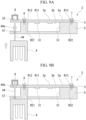
FIGS. 9 and 9B , a receivingmember 8 may be provided on thefirst surface 3a of thecircuit board 3. The receivingmember 8 supports thecircuit board 3 from above when the press-fit terminals 44 are press-fitted into the terminal holes 32. The receivingmember 8 is provided to surround the plurality of terminal holes 32. The receivingmember 8 supports both side portions of the terminal holes 32 in the second direction D2, at thecircuit board 3. A pressing force applied to thecircuit board 3 when the press-fit terminals 44 are press-fitted into the terminal holes 32 is received by the receivingmember 8 from above, so that the distortion of thecircuit board 3 can be more effectively suppressed. - The receiving
member 8 may be configured to support only one side portion of the terminal holes 32 in the second direction D2, at thecircuit board 3. For example, the receivingmember 8 may be disposed only between theterminal holes 32 and the terminal-side supported portion R12. - Hereinafter, a
circuit connection device 2A according to a second embodiment will be described with reference toFIGS. 10 to 12B . Components having the same functions and actions as those in the first embodiment are denoted by the same reference signs, and a description thereof will be omitted. - As shown in
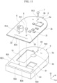
FIG. 11 , in the present embodiment, thecircuit board 3 further includes a second terminal-side supported portion R14 (second supported portion). The second terminal-side supported portion R14 is disposed on a side opposite to the terminal-side supported portion R12 with the plurality ofterminal holes 32 interposed therebetween. Namely, the plurality ofterminal holes 32 are disposed between the terminal-side supported portion R12 and the second terminal-side supported portion R14. In the second terminal-side supported portion R14, thesecond surface 3b of thecircuit board 3 is in contact with thesupport surface 5a of theboard support member 5. The second terminal-side supported portion R14 is supported by theboard support member 5. - The
board support member 5 further includes a second terminal-side supporting portion R24 (second supporting portion). The second terminal-side supporting portion R24 is provided at a position corresponding to the second terminal-side supported portion R14 of thecircuit board 3. The second terminal-side supporting portion R24 supports the second terminal-side supported portion R14 from below. - In the present embodiment, the pair of side portions R23 connect both ends of the terminal-side supporting portion R21 in the first direction D1 and both ends of the second terminal-side supporting portion R24 in the first direction D1. A second accommodating recessed
portion 55A (accommodating recessed portion) partitioned by the terminal-side supporting portion R21, the second terminal-side supporting portion R24, and the pair of side portions R23 is provided on thesupport surface 5a of theboard support member 5. The second accommodating recessedportion 55A is a closed space surrounded by the terminal-side supporting portion R21, the second terminal-side supporting portion R24, and the pair of side portions R23. The distal end portions of the press-fit terminals 44 press-fitted into the terminal holes 32 are accommodated in the second accommodating recessedportion 55A. The press-fit terminals 44 are press-fitted into the terminal holes 32 toward the lower side. - In the present embodiment as well, the same effect as that of first embodiment can be achieved. Namely, according to the
circuit connection device 2A of the present embodiment, it is possible to suppress the distortion of thecircuit board 3 and prevent damage to theelectronic components 31 mounted on thecircuit board 3 while suppressing an increase in the number of components. - In addition, the
circuit board 3 further includes the second terminal-side supported portion R14 supported by theboard support member 5. Theterminal hole 32 is disposed between the terminal-side supported portion R12 and the second terminal-side supported portion R14. - A pressing force applied to the
circuit board 3 when the press-fit terminal 44 is press-fitted into theterminal hole 32 can be received by the second terminal-side supported portion R14 in addition to the terminal-side supported portion R12. Therefore, the distortion of thecircuit board 3 can be more reliably suppressed. - In addition, the
board support member 5 includes the terminal-side supporting portion R21 that supports the terminal-side supported portion R12, the second terminal-side supporting portion R24 that supports the second terminal-side supported portion R14, and the second accommodating recessedportion 55A that is disposed between the terminal-side supporting portion R21 and the second terminal-side supporting portion R24, and that accommodates the distal end of the press-fit terminal 44 press-fitted into theterminal hole 32. The second accommodating recessedportion 55A is surrounded by the terminal-side supporting portion R21, the second terminal-side supporting portion R24, and the pair of side portions R23 connecting the terminal-side supporting portion R21 and the second terminal-side supporting portion R24. - There is a possibility that fine metal debris may be generated when the press-
fit terminal 44 is press-fitted into theterminal hole 32. Since the second accommodating recessedportion 55A is a closed space surrounded by the terminal-side supporting portion R21, the second terminal-side supporting portion R24, and the pair of side portions R23, the metal debris can be prevented from scattering to the outside of the second accommodating recessedportion 55A. Therefore, the metal debris can be prevented from adhering to various circuits and the like of thecircuit board 3, such that it is possible to prevent a short circuit. In addition, foreign matter can be prevented from entering the second accommodating recessedportion 55A from the outside. Therefore, it is possible to prevent a malfunction of thecircuit board 3 or the generation of an oxide on thecircuit board 3 and theconnector 4 due to adhesion of foreign matter from the outside to the press-fit terminal 44 or theterminal hole 32. - As shown in
FIGS. 13A and 13B , the press-fit terminals 44 may be press-fitted into the terminal holes 32 toward the upper side. In this case, theconnector 4 is disposed on thesecond surface 3b side of thecircuit board 3. Theboard support member 5 is disposed between thecircuit board 3 and theconnector 4. The terminal through-holes 57 through which the press-fit terminals 44 are inserted are formed in theboard support member 5. The press-fit terminals 44 are inserted through the terminal through-holes 57, and are press-fitted into the terminal holes 32. - In addition, the second terminal-side supporting portion R24 may come into contact with the
first surface 3a of thecircuit board 3 to support the second terminal-side supported portion R14 from above. In this case, a pressing force applied to thecircuit board 3 when the press-fit terminals 44 are press-fitted into the terminal holes 32 can be more effectively received by the second terminal-side supporting portion R24, and the distortion of thecircuit board 3 can be more effectively suppressed. - Hereinafter, a
circuit connection device 2B according to a third embodiment will be described with reference toFIGS. 14A and 14B . Components having the same functions and actions as those in the first embodiment and the second embodiment are denoted by the same reference signs, and a description thereof will be omitted. -
FIGS. 14A and 14B are views showing a schematic configuration of thecircuit connection device 2B.FIG. 14B is a view of thecircuit connection device 2B when viewed in the second direction D2. - As shown in
FIG. 14A and FIG. 14B , the present embodiment is different from the second embodiment in that aviewing hole 58 is formed in theboard support member 5. Theviewing hole 58 is formed in the second terminal-side supporting portion R24. Theviewing hole 58 is formed such that the distal ends of the press-fit terminals 44 accommodated in the second accommodating recessedportion 55A are visible from the outside. When viewed in the second direction D2, theviewing hole 58 is formed at a position overlapping the distal ends of the plurality of press-fit terminals 44. Theviewing hole 58 has a size that allows all the distal ends of the plurality of press-fit terminals 44 to be visible by asingle viewing hole 58. - The press-fit state of the press-
fit terminals 44 into the terminal holes 32 can be confirmed through theviewing hole 58 from the outside of thecircuit connection device 2B. Therefore, it is possible to prevent a connection failure between thecircuit board 3 and theconnector 4, a malfunction of thecircuit board 3, and the like due to poor press-fitting of the press-fit terminals 44 into the terminal holes 32. For example, when the distal ends of the press-fit terminals 44 cannot be confirmed from theviewing hole 58, or when the protrusion amount of the press-fit terminals 44 visible from theviewing hole 58 is insufficient, it is determined that poor press-fitting of the press-fit terminals 44 into the terminal holes 32 has occurred. - As shown in
FIG. 15 , a plurality of viewing holes 58 may be formed to correspond to the plurality of press-fit terminals 44. Alternatively, the plurality of viewing holes 58 may be formed such that two or more press-fit terminals 44 are visible through oneviewing hole 58. - Hereinafter, a
circuit connection device 2C according to a fourth embodiment will be described with reference toFIGS. 16A and 16B . Components having the same functions and actions as those in the first to third embodiments are denoted by the same reference signs, and a description thereof will be omitted. - As shown in
FIGS. 16A and 16B , in the present embodiment, thecircuit board 3 further includes a second mounting portion R15 and an end portion-side supported portion R16. - Second
electronic components 63 are mounted on the second mounting portion R15. The second mounting portion R15 is disposed on a side opposite to the terminal holes 32 with the second terminal-side supported portion R14 interposed therebetween. Namely, the second terminal-side supported portion R14 is disposed between the second mounting portion R15 and the terminal holes 32. - The end portion-side supported portion R16 is disposed on a side opposite to the second terminal-side supported portion R14 with the second mounting portion R15 interposed therebetween. Namely, the second mounting portion R15 is disposed between the second terminal-side supported portion R14 and the end portion-side supported portion R16. In the end portion-side supported portion R16, the
second surface 3b of thecircuit board 3 is in contact with thesupport surface 5a of theboard support member 5. The end portion-side supported portion R16 is supported by theboard support member 5. The end portion-side supported portion R16 may be disposed inside the second mounting portion R15. - The
board support member 5 further includes an end portion-side supporting portion R25. The end portion-side supporting portion R25 is provided at a position corresponding to the end portion-side supported portion R16. The end portion-side supporting portion R25 supports the end portion-side supported portion R16 from below. - A third accommodating recessed
portion 64 that accommodates the secondelectronic components 63 mounted on thesecond surface 3b of thecircuit board 3 is provided on thesupport surface 5a of theboard support member 5. The third accommodating recessedportion 64 is provided at a position corresponding to the second mounting portion R15. - The second terminal-side supported portion R14 of the
circuit board 3 and the second terminal-side supporting portion R24 of theboard support member 5 are fastened to each other bythird fastening members 61. Thethird fastening members 61 are, for example, screws. Fastening holes into which thethird fastening members 61 are mounted are formed in the second terminal-side supported portion R14 and the second terminal-side supporting portion R24. Thethird fastening members 61 fix thecircuit board 3 to theboard support member 5 in a state where thecircuit board 3 is pressed toward theboard support member 5. - The end portion-side supported portion R16 of the
circuit board 3 and the end portion-side supporting portion R25 of theboard support member 5 are fastened to each other byfourth fastening members 62. Thefourth fastening members 62 are, for example, screws. Fastening holes into which thefourth fastening members 62 are mounted are formed in the end portion-side supported portion R16 and the end portion-side supporting portion R25. Thefourth fastening members 62 fix thecircuit board 3 to theboard support member 5 in a state where thecircuit board 3 is pressed toward theboard support member 5. - In the present embodiment as well, the same effect as that of first embodiment can be achieved. Namely, according to the
circuit connection device 2C of the present embodiment, it is possible to suppress the distortion of thecircuit board 3 and prevent damage to theelectronic components 31 mounted on thecircuit board 3 while suppressing an increase in the number of components. - In addition, the
circuit board 3 further includes the second mounting portion R15 on which the secondelectronic component 63 is mounted. The second terminal-side supported portion R14 is disposed between the second mounting portion R15 and theterminal hole 32. - The mounting regions of the
electronic components board support member 5 is disposed between the second mounting portion R15 and theterminal hole 32. Therefore, a pressing force applied to thecircuit board 3 when the press-fit terminal 44 is press-fitted into theterminal hole 32 can be received by the second terminal-side supported portion R14, and the pressing force can be prevented from being directly transmitted to the second mounting portion R15. Therefore, the distortion of thecircuit board 3 can be suppressed, and the secondelectronic component 63 mounted on the second mounting portion R15 can be prevented from being damaged. - Hereinafter, a
circuit connection device 2D according to a fifth embodiment will be described with reference toFIG. 17 . Components having the same functions and actions as those in the first to fourth embodiments are denoted by the same reference signs, and a description thereof will be omitted. - In the present embodiment, the
board support member 5 and thefirst fastening members 6 are made of metal. In addition, as shown inFIG. 17 , anoise suppression component 31B as theelectronic component 31 is mounted on thefirst surface 3a of thecircuit board 3. Thenoise suppression component 31B includes an X capacitor and a Y capacitor. Thenoise suppression component 31B is disposed in proximity to the terminal-side supported portion R12 of thecircuit board 3. - A GND pattern 71 (electrical connection portion) is provided on the terminal-side supported portion R12. The
GND pattern 71 is disposed on thefirst surface 3a of thecircuit board 3. The X capacitor and the Y capacitor of thenoise suppression component 31B are electrically connected to theGND pattern 71. When thefirst fastening member 6 is fastened to thecircuit board 3, thefirst fastening member 6 comes into contact with theGND pattern 71, and theGND pattern 71 and thefirst fastening member 6 are electrically connected to each other. - The
board support member 5 is electrically connected to a ground (GND). When thefirst fastening members 6 are fastened to theboard support member 5, thefirst fastening members 6 come into contact with theboard support member 5, and thefirst fastening members 6 and theboard support member 5 are electrically connected to each other. Therefore, the X capacitor and the Y capacitor of thenoise suppression component 31B are connected to the GND via theGND pattern 71, thefirst fastening member 6, and theboard support member 5. - In the present embodiment as well, the same effect as that of first embodiment can be achieved. Namely, according to the
circuit connection device 2D of the present embodiment, it is possible to suppress the distortion of thecircuit board 3 and prevent damage to theelectronic component 31 mounted on thecircuit board 3 while suppressing an increase in the number of components. - In addition, the
board support member 5 is made of metal, and is electrically connected to the GND. Thefirst fastening member 6 is made of metal, and is electrically connected to theboard support member 5. TheGND pattern 71 that electrically connects thenoise suppression component 31B as theelectronic component 31 and thefirst fastening member 6 is formed on the terminal-side supported portion R12. - Accordingly, the
noise suppression component 31B can be connected to the GND via theboard support member 5 and thefirst fastening member 6. - In addition, when the
noise suppression component 31B is disposed at a position close to the terminal-side supported portion R12 (namely, a position close to the terminal hole 32) on the mounting portion R11, thenoise suppression component 31B can effectively remove noise of power supply and signals. For example, when power is supplied from the press-fit terminal 44 to theelectronic component 31 via theterminal hole 32, thenoise suppression component 31B can remove noise of the power supply immediately after being input to the mounting portion R11. When signals are output from theelectronic component 31 to the press-fit terminal 44 via theterminal hole 32, thenoise suppression component 31B can remove noise of the signals immediately before theterminal hole 32. - In addition, since the distortion of the mounting portion R11 can be suppressed by the terminal-side supported portion R12, a ceramic capacitor or the like having small distortion resistance but being small in size can be used as the
noise suppression component 31B. Therefore, thecircuit board 3 can be miniaturized. - As shown in
FIG. 18 , theGND pattern 71 may be formed to extend to thesecond surface 3b of thecircuit board 3 in the terminal-side supported portion R12. In this case, theGND pattern 71 is directly connected to theboard support member 5. The X capacitor and the Y capacitor of thenoise suppression component 31B are connected to the GND via theGND pattern 71 and theboard support member 5. - Hereinafter, a
circuit connection device 2E according to a sixth embodiment will be described with reference toFIGS. 19A and 19B . Components having the same functions and actions as those in the first to fifth embodiments are denoted by the same reference signs, and a description thereof will be omitted. - As shown in
FIGS. 19A and 19B , in the present embodiment, thecircuit board 3 and theconnector 4 are connected to each other using a multipole connector. - The
connector 4 includes a recessedconnector component 81 instead of the plurality of press-fit terminals 44. The recessedconnector component 81 includes a plurality ofconnection terminals 81a disposed side by side in the first direction D1, and a holdingmember 81b that holds the plurality ofconnection terminals 81a. The holdingmember 81b includes a recessed portion, and the plurality ofconnection terminals 81a are disposed inside the recessed portion. - The
circuit board 3 includes a protrudingconnector component 82. The protrudingconnector component 82 includes a plurality of connectionfit portions 82a (terminal holes) disposed side by side in the first direction D1, and a holdingmember 82b that holds the plurality of connectionfit portions 82a. One end portions of the plurality of connectionfit portions 82a are fitted to the plurality ofconnection terminals 81a. The other end portions 82a1 of the plurality of connectionfit portions 82a are fixed to thecircuit board 3, for example, by soldering. - The
circuit board 3 and theconnector 4 are electrically connected to each other by respectively fitting the plurality ofconnection terminals 81a into the one end portions of the plurality of connectionfit portions 82a. When theconnection terminals 81a are fitted into the one end portions of the connectionfit portions 82a, a pressing force is applied to thecircuit board 3. The terminal-side supported portion R12 supported by theboard support member 5 is disposed between the mounting portion R11 on which theelectronic components 31 are mounted and the terminal holes 32. Therefore, the pressing force applied to thecircuit board 3 when theconnection terminals 81a are fitted to the one end portions of the connectionfit portions 82a can be received by the terminal-side supported portion R12, and the pressing force can be prevented from being directly transmitted to the mounting portion R11. Therefore, the distortion of thecircuit board 3 can be suppressed, and theelectronic components 31 mounted on the mounting portion R11 can be prevented from being damaged. In addition, theelectronic components 31 are mounted on thecircuit board 3, and the connectionfit portions 82a into which theconnection terminals 81a are press-fitted are formed on thecircuit board 3. Therefore, compared to a case where a parent board on which electronic components are mounted and a child board to which connection terminals are connected are separately provided, an increase in the number of components of thecircuit connection device 2E can be suppressed. As described above, according to thecircuit connection device 2E of the present embodiment, it is possible to suppress the distortion of thecircuit board 3 and prevent damage to theelectronic components 31 mounted on thecircuit board 3 while suppressing an increase in the number of components. - The embodiments can be combined, and each embodiment can be modified or omitted as appropriate.
- For example, the numbers of the press-
fit terminals 44, thefirst fastening members 6, thesecond fastening members 7, and the like are appropriately changed according to the specifications of the rotatingelectrical machine device 100. - The
first fastening member 6 and thesecond fastening member 7 are not limited to screws as long as they are able to fix thecircuit board 3 to theboard support member 5. - The
board support member 5 may be integrally formed with thecase 14 of the rotatingelectrical machine 1. - The plurality of
terminal holes 32 may be disposed at an end portion on one side in the first direction D1. In this case, for example, the mounting portion R11 may be disposed at an end portion on the other side in the first direction D1, and the terminal-side supported portion R12 may be disposed to be interposed between the mounting portion R11 and the terminal holes 32 in the first direction D1. The plurality ofterminal holes 32 may be disposed in combination at the end portion on the one side in the first direction D1 and the end portion on the one side in the second direction D2. -
- 1: Rotating electrical machine
- 2, 2A, 2B, 2C, 2D, 2E: Circuit connection device
- 3: Circuit board
- 4: Connector
- 5: Board support member
- 6: First fastening member (fixing member)
- 31: Electronic component
- 31B: Noise suppression component
- 32: Terminal hole
- 44: Press-fit terminal (connection terminal)
- 55A: Second accommodating recessed portion (accommodating recessed portion)
- 58: Viewing hole
- 63: Second electronic component
- 71: GND pattern (electrical connection portion)
- 81a: Connection terminal
- 82a: Connection fit portion (terminal hole)
- R11: Mounting portion
- R12: Terminal-side supported portion (supported portion)
- R14: Second terminal-side supported portion (second supported portion)
- R15: Second mounting portion
- R21: Terminal-side supporting portion (supporting portion)
- R23: Side portion
- R24: Second terminal-side supporting portion (second supporting portion)
- 100: Rotating electrical machine device
Claims (10)
- A circuit connection device comprising:a connector including a connection terminal connected to an outside;a circuit board on which an electronic component is mounted and in which a terminal hole into which the connection terminal is press-fitted is formed;a board support member that supports the circuit board; anda fixing member that fixes the circuit board to the board support member,wherein the circuit board includes a mounting portion on which the electronic component is mounted, and a supported portion fixed to the board support member by the fixing member and supported by the board support member, andthe supported portion is disposed between the mounting portion and the terminal hole.
- The circuit connection device according to Claim 1,wherein the circuit board further includes a second supported portion supported by the board support member, andthe terminal hole is disposed between the supported portion and the second supported portion.
- The circuit connection device according to Claim 2,
wherein the board support member includes:a supporting portion that supports the supported portion of the circuit board;a second supporting portion that supports the second supported portion of the circuit board; andan accommodating recessed portion that is disposed between the supporting portion and the second supporting portion and that accommodates a distal end of the connection terminal press-fitted into the terminal hole, andthe accommodating recessed portion is surrounded by the supporting portion, the second supporting portion, and a pair of side portions connecting the supporting portion and the second supporting portion. - The circuit connection device according to Claim 3,
wherein a viewing hole through which the distal end of the connection terminal accommodated in the accommodating recessed portion is visible from the outside is formed in the board support member. - The circuit connection device according to any one of Claims 2 to 4,wherein the circuit board further includes a second mounting portion on which a second electronic component is mounted, andthe second supported portion is disposed between the second mounting portion and the terminal hole.
- The circuit connection device according to any one of Claims 1 to 5,
wherein in a case where a side on which the board support member is located when viewed from the circuit board is defined as a lower side, the connection terminal is press-fitted into the terminal hole toward the lower side. - The circuit connection device according to any one of Claims 1 to 5,
wherein in a case where a side on which the circuit board is located when viewed from the board support member is defined as an upper side, the connection terminal is press-fitted into the terminal hole toward the upper side. - The circuit connection device according to any one of Claims 1 to 7,wherein the board support member is made of metal, and is electrically connected to a GND,the fixing member is made of metal, and is electrically connected to the board support member, andan electrical connection portion that electrically connects a noise suppression component as the electronic component and the fixing member is formed on the supported portion.
- The circuit connection device according to any one of Claims 1 to 8,
wherein the supported portion is disposed at a position overlapping the connector when viewed in a thickness direction of the circuit board. - A rotating electrical machine device comprising:a rotating electrical machine; andthe circuit connection device according to any one of Claims 1 to 9 configured to control the rotating electrical machine.
Applications Claiming Priority (1)
| Application Number | Priority Date | Filing Date | Title |
|---|---|---|---|
| PCT/JP2022/020622 WO2023223449A1 (en) | 2022-05-18 | 2022-05-18 | Circuit connection device and rotating electrical machine device |
Publications (2)
| Publication Number | Publication Date |
|---|---|
| EP4529371A1 true EP4529371A1 (en) | 2025-03-26 |
| EP4529371A4 EP4529371A4 (en) | 2025-07-09 |
Family
ID=88834894
Family Applications (1)
| Application Number | Title | Priority Date | Filing Date |
|---|---|---|---|
| EP22942654.9A Pending EP4529371A4 (en) | 2022-05-18 | 2022-05-18 | CIRCUIT CONNECTION DEVICE AND ELECTRICAL LATHE DEVICE |
Country Status (5)
| Country | Link |
|---|---|
| US (1) | US20250158478A1 (en) |
| EP (1) | EP4529371A4 (en) |
| JP (1) | JP7651069B2 (en) |
| CN (1) | CN119138113A (en) |
| WO (1) | WO2023223449A1 (en) |
Family Cites Families (13)
| Publication number | Priority date | Publication date | Assignee | Title |
|---|---|---|---|---|
| JP2001196770A (en) * | 2000-01-12 | 2001-07-19 | Omron Corp | control unit |
| JP4427896B2 (en) * | 2000-03-17 | 2010-03-10 | 株式会社デンソー | Vehicle alternator |
| JP2003051688A (en) * | 2001-08-08 | 2003-02-21 | Shindengen Electric Mfg Co Ltd | Electronic circuit device |
| DE102005043033B3 (en) * | 2005-09-09 | 2007-04-12 | Siemens Ag | Pressfit system for electrical contacting and method for mounting the Pressfit system |
| GB2464622B (en) * | 2008-09-18 | 2010-10-20 | Controlled Power Technologies | A power terminal in an intergrated starter generator |
| JP6432395B2 (en) * | 2015-03-05 | 2018-12-05 | 株式会社デンソー | Electronic equipment |
| JP2017175069A (en) * | 2016-03-25 | 2017-09-28 | 株式会社デンソー | Electronic control device |
| JP2018037568A (en) * | 2016-09-01 | 2018-03-08 | Kyb株式会社 | Electronic device |
| BR112019025288B1 (en) * | 2017-06-01 | 2023-12-19 | Nsk Ltd | ELECTRIC DRIVING DEVICE AND ELECTRIC POWER 1`STEERING DEVICE |
| JP7157740B2 (en) * | 2017-07-14 | 2022-10-20 | 日立Astemo株式会社 | Electronic control device and method for manufacturing electronic control device |
| JP2020047769A (en) * | 2018-09-19 | 2020-03-26 | 日立オートモティブシステムズ株式会社 | Electronic control apparatus and manufacturing method of electronic control apparatus |
| JP7359022B2 (en) | 2020-02-14 | 2023-10-11 | 株式会社デンソー | drive device |
| CN117121352A (en) * | 2021-04-28 | 2023-11-24 | 三菱电机株式会社 | Controls, drives and electric power steering |
-
2022
- 2022-05-18 CN CN202280093671.XA patent/CN119138113A/en active Pending
- 2022-05-18 JP JP2024521447A patent/JP7651069B2/en active Active
- 2022-05-18 WO PCT/JP2022/020622 patent/WO2023223449A1/en not_active Ceased
- 2022-05-18 US US18/839,649 patent/US20250158478A1/en active Pending
- 2022-05-18 EP EP22942654.9A patent/EP4529371A4/en active Pending
Also Published As
| Publication number | Publication date |
|---|---|
| US20250158478A1 (en) | 2025-05-15 |
| CN119138113A (en) | 2024-12-13 |
| JP7651069B2 (en) | 2025-03-25 |
| JPWO2023223449A1 (en) | 2023-11-23 |
| WO2023223449A1 (en) | 2023-11-23 |
| EP4529371A4 (en) | 2025-07-09 |
Similar Documents
| Publication | Publication Date | Title |
|---|---|---|
| JP5239413B2 (en) | motor | |
| CN103459236B (en) | Drive Unit Integrated Rotating Motor | |
| JPWO2020067255A1 (en) | motor | |
| JP2017518731A (en) | Brush holding device for commutator | |
| EP1445835B1 (en) | Grounding arrangement for an electric motor with an encoder | |
| JP2017516453A (en) | Brush holding device for commutator | |
| JP2017519480A (en) | Brush holding device for commutator | |
| CN101278448B (en) | Motor connection plate and motor | |
| JP4582182B2 (en) | Electric power steering device | |
| EP4529371A1 (en) | Circuit connection device and rotating electrical machine device | |
| CN114830504B (en) | Rotary motor | |
| US20100253166A1 (en) | Rotor and Vibration Motor | |
| JP4702593B2 (en) | motor | |
| JP7231398B2 (en) | Rotating electric machine | |
| CN117559730A (en) | Motor with a motor housing | |
| JP7615976B2 (en) | Manufacturing method of drive device, and drive device | |
| JP7638443B2 (en) | Drive unit | |
| JP7647464B2 (en) | Drive unit | |
| JP7442745B2 (en) | Circuit connection device, rotating electric machine device, and manufacturing method of circuit connection device | |
| JP2024069902A (en) | Drive unit | |
| JP7471526B2 (en) | Circuit connection device, rotating electrical machine device, and method for manufacturing the circuit connection device | |
| JP2007020266A (en) | Electric motor | |
| JP2006187109A (en) | Brushless motor | |
| JP6169937B2 (en) | Inspection method of motor with control circuit | |
| JP2003079088A (en) | AC servo motor |
Legal Events
| Date | Code | Title | Description |
|---|---|---|---|
| STAA | Information on the status of an ep patent application or granted ep patent |
Free format text: STATUS: THE INTERNATIONAL PUBLICATION HAS BEEN MADE |
|
| PUAI | Public reference made under article 153(3) epc to a published international application that has entered the european phase |
Free format text: ORIGINAL CODE: 0009012 |
|
| STAA | Information on the status of an ep patent application or granted ep patent |
Free format text: STATUS: REQUEST FOR EXAMINATION WAS MADE |
|
| 17P | Request for examination filed |
Effective date: 20240822 |
|
| AK | Designated contracting states |
Kind code of ref document: A1 Designated state(s): AL AT BE BG CH CY CZ DE DK EE ES FI FR GB GR HR HU IE IS IT LI LT LU LV MC MK MT NL NO PL PT RO RS SE SI SK SM TR |
|
| REG | Reference to a national code |
Ref country code: DE Ref legal event code: R079 Free format text: PREVIOUS MAIN CLASS: H05K0007140000 Ipc: H02K0005220000 |
|
| A4 | Supplementary search report drawn up and despatched |
Effective date: 20250611 |
|
| RIC1 | Information provided on ipc code assigned before grant |
Ipc: H05K 7/14 20060101ALI20250604BHEP Ipc: H02K 11/40 20160101ALI20250604BHEP Ipc: H02K 11/33 20160101ALI20250604BHEP Ipc: H02K 11/215 20160101ALI20250604BHEP Ipc: H02K 5/22 20060101AFI20250604BHEP |
|
| DAV | Request for validation of the european patent (deleted) | ||
| DAX | Request for extension of the european patent (deleted) |