EP4528944A2 - Vorrichtung und verfahren zur laserdiodenkalibrierung - Google Patents
Vorrichtung und verfahren zur laserdiodenkalibrierung Download PDFInfo
- Publication number
- EP4528944A2 EP4528944A2 EP24196826.2A EP24196826A EP4528944A2 EP 4528944 A2 EP4528944 A2 EP 4528944A2 EP 24196826 A EP24196826 A EP 24196826A EP 4528944 A2 EP4528944 A2 EP 4528944A2
- Authority
- EP
- European Patent Office
- Prior art keywords
- photodiode
- laser diode
- current
- resistance value
- anode
- Prior art date
- Legal status (The legal status is an assumption and is not a legal conclusion. Google has not performed a legal analysis and makes no representation as to the accuracy of the status listed.)
- Pending
Links
Images


Classifications
-
- H—ELECTRICITY
- H01—ELECTRIC ELEMENTS
- H01S—DEVICES USING THE PROCESS OF LIGHT AMPLIFICATION BY STIMULATED EMISSION OF RADIATION [LASER] TO AMPLIFY OR GENERATE LIGHT; DEVICES USING STIMULATED EMISSION OF ELECTROMAGNETIC RADIATION IN WAVE RANGES OTHER THAN OPTICAL
- H01S5/00—Semiconductor lasers
- H01S5/06—Arrangements for controlling the laser output parameters, e.g. by operating on the active medium
- H01S5/0617—Arrangements for controlling the laser output parameters, e.g. by operating on the active medium using memorised or pre-programmed laser characteristics
-
- H—ELECTRICITY
- H01—ELECTRIC ELEMENTS
- H01S—DEVICES USING THE PROCESS OF LIGHT AMPLIFICATION BY STIMULATED EMISSION OF RADIATION [LASER] TO AMPLIFY OR GENERATE LIGHT; DEVICES USING STIMULATED EMISSION OF ELECTROMAGNETIC RADIATION IN WAVE RANGES OTHER THAN OPTICAL
- H01S5/00—Semiconductor lasers
- H01S5/04—Processes or apparatus for excitation, e.g. pumping, e.g. by electron beams
- H01S5/042—Electrical excitation ; Circuits therefor
- H01S5/0425—Electrodes, e.g. characterised by the structure
- H01S5/04256—Electrodes, e.g. characterised by the structure characterised by the configuration
-
- H—ELECTRICITY
- H01—ELECTRIC ELEMENTS
- H01S—DEVICES USING THE PROCESS OF LIGHT AMPLIFICATION BY STIMULATED EMISSION OF RADIATION [LASER] TO AMPLIFY OR GENERATE LIGHT; DEVICES USING STIMULATED EMISSION OF ELECTROMAGNETIC RADIATION IN WAVE RANGES OTHER THAN OPTICAL
- H01S5/00—Semiconductor lasers
- H01S5/02—Structural details or components not essential to laser action
- H01S5/026—Monolithically integrated components, e.g. waveguides, monitoring photo-detectors, drivers
- H01S5/0262—Photo-diodes, e.g. transceiver devices, bidirectional devices
-
- H—ELECTRICITY
- H01—ELECTRIC ELEMENTS
- H01S—DEVICES USING THE PROCESS OF LIGHT AMPLIFICATION BY STIMULATED EMISSION OF RADIATION [LASER] TO AMPLIFY OR GENERATE LIGHT; DEVICES USING STIMULATED EMISSION OF ELECTROMAGNETIC RADIATION IN WAVE RANGES OTHER THAN OPTICAL
- H01S5/00—Semiconductor lasers
- H01S5/06—Arrangements for controlling the laser output parameters, e.g. by operating on the active medium
- H01S5/068—Stabilisation of laser output parameters
- H01S5/0683—Stabilisation of laser output parameters by monitoring the optical output parameters
Definitions
- Embodiments of the present disclosure generally relate to imaging systems, and, more particularly, to imaging systems comprising laser diodes.
- laser illumination devices are used to generate laser light.
- Some of these laser illumination devices comprise a laser diode (often a Vertical Cavity Surface Emitting Laser or VCSEL) to generate the laser light and a photodiode to provide feedback.
- the laser diode and the photodiode are often integrated into a single package.
- a laser driver also termed a laser diode drive
- the photodiode current is used as feedback to keep the optical power level of the laser the same by adjusting the current source output. This is called Constant Power Mode.
- the photodiode current is proportional to the optical power output of the laser diode.
- the optical power output of the laser diode changes (typically reduces) due to changes in the temperature of the laser diode body over time and resistive heating.
- the laser driver detects the change in the photodiode current and adjusts the output of the laser drive to the laser diode to maintain the desired optical power output.
- each laser diode / photodiode package is typically calibrated once before starting its usage.
- the laser diode / photodiode package may also be calibrated as needed during its operational life.
- the calibration process for conventional laser diode / photodiode packages is complex and time-consuming.
- Various embodiments described herein relate to laser illumination devices and associated biasing a photodiode of laser illumination devices and methods of calibrating laser illumination devices.
- a laser illumination device comprises a laser diode having an anode and a cathode, a photodiode having an anode and a cathode connected to the cathode of the laser diode, a laser diode driver having a voltage output connected to the anode of the laser diode and a feedback input connected to the anode of the photodiode, and a variable resistor with a selectable resistance value connected between the anode of the photodiode and ground. The selectable resistance value is selected to maintain a reference voltage on the anode of the photodiode to reverse bias the photodiode.
- variable resistor with the selectable resistance value comprises a digital potentiometer.
- the laser illumination device further comprises a microcontroller in communication with the digital potentiometer for selecting the selectable resistance value.
- the laser illumination device further comprises first and second resistors connected in series between the cathodes of the laser diode and the photodiode and ground, and a current sense analog-to-digital controller (ADC) connected in parallel across one of the first and second resistors for measuring current through the one of the first and second resistors.
- ADC analog-to-digital controller
- the laser illumination device further comprises a fixed resistor connected in series with the variable resistor.
- the reference voltage is 1.24 volts and the fixed resistor has a resistance value of 6200 ohms.
- variable resistor has a selectable resistance value of between 0 and 50,000 ohms.
- a method of method of biasing a photodiode of a laser illumination device comprises connecting a cathode of a laser diode to a cathode of a photodiode, connecting an output of a laser diode driver to an anode of the laser diode, connecting an anode of the photodiode to a feedback input of the laser diode driver, connecting a variable resistor with a selectable resistance value between the anode of the photodiode and ground, and selecting a resistance value of the variable resistor to maintain a reference voltage on the anode of the photodiode to reverse bias the photodiode.
- a method of method of calibrating a laser illumination device comprises connecting a cathode of a laser diode to a cathode of a photodiode, connecting an output of a laser diode driver to an anode of the laser diode, connecting an anode of the photodiode to a feedback input of the laser diode driver, connecting a variable resistor with a selectable resistance value between the anode of the photodiode and ground, for each of a plurality of different selected resistance values of the variable resistor, determining a photodiode current and a laser diode current, for each pair of adjacent values of the plurality of different selected resistance values of the variable resistor, calculating a ratio of (i) a difference between the photodiode current at a second selected resistance value and the photodiode current at a first selected resistance value and (ii) a difference between the laser dio
- the term "comprising” means including but not limited to and should be interpreted in the manner it is typically used in the patent context. Use of broader terms such as comprises, includes, and having should be understood to provide support for narrower terms such as consisting of, consisting essentially of, and comprised substantially of.
- component or feature may,” “can,” “could,” “should,” “would,” “preferably,” “possibly,” “typically,” “optionally,” “for example,” “as an example,” “in some examples,” “often,” or “might” (or other such language) be included or have a characteristic, that specific component or feature is not required to be included or to have the characteristic. Such component or feature may be optionally included in some examples, or it may be excluded.
- various embodiments of the present disclosure overcome the above technical challenges and difficulties and provide various technical improvements and advantages.
- various embodiments of the present disclosure provide an example laser illumination device.
- Various embodiments of the present disclosure provide an example method of biasing a photodiode of a laser illumination device.
- Various embodiments of the present disclosure provide an example method of calibrating a laser illumination device.
- a laser driver monitors photodiode current as feedback by forward biasing the photodiode.
- the response of a photodiode at its forward biased region is non-linear to the optical power.
- calculation intensive methods like linear interpolation are conventionally used during calibration of the laser diode / photodiode package, resulting in a calibration algorithm that consumes a significant amount of time to calculate the required parameters.
- a laser illumination device (which may also be termed a laser light source or a laser source) comprises a laser diode having an anode and a cathode, a photodiode having an anode and a cathode connected to the cathode of the laser diode, a laser diode driver having a voltage output connected to the anode of the laser diode and a feedback input connected to the anode of the photodiode, and a variable resistor with a selectable resistance value connected between the anode of the photodiode and ground.
- the selectable resistance value is selected to maintain a reference voltage on the anode of the photodiode to reverse bias the photodiode.
- a laser illumination device of embodiments of the present disclosure is used with any suitable imaging device or for any suitable imaging method.
- a laser illumination device of embodiments of the present disclosure is used with a peritoneal dialysis device.
- Peritoneal dialysis removes waste and extra fluid through the blood vessels that line the walls of a patient's abdomen. Peritoneal dialysis involves inserting a catheter through the patient's abdominal wall and pumping a dialysis solution into the abdominal cavity. After a set amount of time, the solution is drained and discarded.
- some of the fluid removed from the patient's abdominal cavity is retained and sent for laboratory analysis to determine, for example, the presence of leukocytes (white blood cells), such as neutrophils, monocytes, and/or lymphocytes.
- leukocytes white blood cells
- some of the fluid removed from the patient's abdominal cavity is analyzed by an imaging device to detect the presence of leukocytes.
- the example device may be a peritoneal dialysis device.
- the example device 100 comprises a processor or processing circuitry 102, memory circuitry 104, input/output circuitry 106, communications circuitry 108, one or more pumps 110, a laser source 112, and a camera 120.
- one or more portions of the example device 100 are configured to execute and perform the operations described herein.
- Processing circuitry 102 may be embodied in a number of different ways. In various embodiments, the use of the terms "processor” or “processing circuitry” should be understood to include a single core processor, a multi-core processor, multiple processors internal to the example device 100, and/or one or more remote or “cloud” processor(s) external to the example device 100. In some example embodiments, processing circuitry 102 may include one or more processing devices configured to perform independently. Alternatively, or additionally, processing circuitry 102 may include one or more processor(s) configured in tandem via a bus to enable independent execution of operations, instructions, pipelining, and/or multithreading.
- the processing circuitry 102 may be configured to execute instructions stored in the memory circuitry 104 or otherwise accessible to the processor. Alternatively, or additionally, the processing circuitry 102 may be configured to execute hard-coded functionality. As such, whether configured by hardware or software methods, or by a combination thereof, processing circuitry 102 may represent an entity (e.g., physically embodied in circuitry) capable of performing operations according to embodiments of the present disclosure while configured accordingly. Alternatively, or additionally, processing circuitry 102 may be embodied as an executor of software instructions, and the instructions may specifically configure the processing circuitry 102 to perform the various algorithms embodied in one or more operations described herein when such instructions are executed. In some embodiments, the processing circuitry 102 includes hardware, software, firmware, and/or a combination thereof that performs one or more operations described herein.
- the processing circuitry 102 (and/or co-processor or any other processing circuitry assisting or otherwise associated with the processor) is/are in communication with the memory circuitry 104 via a bus for passing information among components of the example device 100.
- Memory or memory circuitry 104 may be non-transitory and may include, for example, one or more volatile and/or non-volatile memories.
- the memory circuitry 104 includes or embodies an electronic storage device (e.g., a computer readable storage medium).
- the memory circuitry 104 is configured to store information, data, content, applications, instructions, or the like, for enabling the example device 100 to carry out various operations and/or functions in accordance with example embodiments of the present disclosure.
- Input/output circuitry 106 may be included in the example device 100. In some embodiments, input/output circuitry 106 may provide output to the user and/or receive input from a user. The input/output circuitry 106 may be in communication with the processing circuitry 102 to provide such functionality. The input/output circuitry 106 may comprise one or more user interface(s). In some embodiments, a user interface may include a display that comprises the interface(s) rendered as a web user interface, an application user interface, a user device, a backend system, or the like.
- the input/output circuitry 106 also includes a keyboard, a mouse, a joystick, a touch screen, touch areas, soft keys a microphone, a speaker, or other input/output mechanisms.
- the processing circuitry 102 and/or input/output circuitry 106 may be configured to control one or more operations and/or functions of one or more user interface elements through computer program instructions (e.g., software and/or firmware) stored on a memory accessible to the processor (e.g., memory circuitry 104, and/or the like).
- the input/output circuitry 106 includes or utilizes a user-facing application to provide input/output functionality to a computing device and/or other display associated with a user.
- the input/output circuitry 106 comprises indicator lights 110.
- Communications circuitry 108 may be included in the example device 100.
- the communications circuitry 108 may include any means such as a device or circuitry embodied in either hardware or a combination of hardware and software that is configured to receive and/or transmit data from/to a network and/or any other device, circuitry, or module in communication with the example device 100.
- the communications circuitry 108 includes, for example, a network interface for enabling communications with a wired or wireless communications network.
- the communications circuitry 108 may include one or more network interface card(s), antenna(s), bus(es), switch(es), router(s), modem(s), and supporting hardware, firmware, and/or software, or any other device suitable for enabling communications via one or more communications network(s).
- the communications circuitry 108 may include circuitry for interacting with an antenna(s) and/or other hardware or software to cause transmission of signals via the antenna(s) and/or to handle receipt of signals received via the antenna(s). In some embodiments, the communications circuitry 108 enables transmission to and/or receipt of data from a user device, one or more sensors, and/or other external computing device(s) in communication with the example device 100.
- the communications circuitry 108 transmits and/or receives (wired or wirelessly) information related to calibration of the laser source 112. In some embodiments, the communications circuitry 108 transmits and/or receives information from other components of the example device 100 using the Inter-Integrated Circuit (I2C) protocol.
- I2C Inter-Integrated Circuit
- One or more pumps 110 may be included in the example device 100. In some embodiments, such pumps pump the dialysis solution into and out of the patient's abdominal cavity.
- a laser source 112 may be included in the example device 100.
- the laser source 112 comprises at least a laser diode 114, a photodiode 116, and a laser diode driver 118, all of which are described further below.
- the laser diode 114 and the photodiode 116 are integrated into a single package.
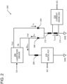
- the laser source also comprises additional components, as described further below in relation to FIG. 2 .
- a camera 120 may be included in the example device 100.
- the camera 120 receives the laser light that has been emitted by the laser source 112 and has passed through a sample of the extracted dialysis solution to capture holographic images of bodily fluids for image analysis for identification of leukocytes.
- two or more of the sets of circuitry 102-108 are combinable. Alternatively, or additionally, one or more of the sets of circuitry 102-108 perform some or all of the operations and/or functionality described herein as being associated with another circuitry. In some embodiments, two or more of the sets of circuitry 102-108 are combined into a single module embodied in hardware, software, firmware, and/or a combination thereof.
- an example device 100 in accordance with the present disclosure may be in other forms.
- an example device 100 may comprise one or more additional and/or alternative elements, and/or may be structured differently than that illustrated in FIG. 1 .
- the example laser source 200 comprises a laser diode driver 202 powered by a 12 volt power supply, a laser diode 204 whose anode is connected to a voltage output (Vout) of the laser diode driver 202, and a photo diode 206 whose cathode is connected to the cathode of the laser diode 204 and whose anode is connected to a feedback input (FB) of the laser diode driver 202.
- Vout voltage output
- FB feedback input
- the example laser source 200 also comprises a fixed value resistor 208 and a variable resistor such as digital potentiometer 210 (which may be abbreviated as DPOT) to provide a variable resistance connected in series between the anode of the photodiode 206 and ground.
- a variable resistor such as digital potentiometer 210 (which may be abbreviated as DPOT) to provide a variable resistance connected in series between the anode of the photodiode 206 and ground.
- the example laser source 200 also comprises a first resistor 212 and a second resistor 214 connected in series between the cathodes of the laser diode 204 and the photo diode 206 and ground, and a current sense analog-to-digital converter (ADC) 216 connected across the second resistor 214 to measure the current flowing through the second resistor 214.
- ADC analog-to-digital converter
- the current flowing through the second resistor 214 is equal to the laser diode current minus the photodiode current and may be used to determine the laser diode current (described further below) since the laser diode current cannot be directly measured or calculated.
- the digital potentiometer 210 communicates with a processor (such as processing circuitry 102) via I2C protocol to receive a signal indicating the desired setting of the digital potentiometer 210.
- the ADC 216 communicates with a processor (such as processing circuitry 102) via I2C protocol to send the measured current.
- the selectable resistance value is selected, in combination with the resistance value of the fixed resistor 208, to maintain a reference voltage (Vref) on the anode of the photodiode 206 to reverse bias the photodiode 206.
- the reference voltage is 1.24 volts, although any suitable reference voltage may be used.
- the fixed resistor 208 is a 6200 ohm resistor, although any suitable resistor value may be used.
- the digital potentiometer 210 has a selectable resistance value of between 0 and 50,000 ohms, although any suitable range of resistance values may be used.
- the resistance value of the digital potentiometer 210 is selectable in 128 increments (typically referred to as steps 0-127) via a 7-bit signal.
- the laser diode driver 202 outputs a voltage (Vout) to the anode of the laser diode 204.
- the output voltage is selected to produce a current (I LD ) through the laser diode 204 to cause the laser diode 204 to emit the desired laser light.
- the photodiode 206 senses the laser light and produces a current (I PD ) in response. Because the photodiode 206 is reverse biased, the response of the photodiode 206 to the received illumination is linear.
- the desired reference voltage (Vref) is maintained on the feedback input of the laser diode driver 202 when the laser diode 204 is producing the desired optical power output. If the optical power output of the laser diode reduces due to a temperature increase, the photodiode current (I PD ) decreases and the reference voltage (Vref) decreases.
- the laser diode driver 202 detects the change and adjusts its output (Vout) to the laser diode 204 to maintain the desired optical power output.
- FIG. 3 provides a flowchart illustrating example steps, processes, procedures, and/or operations in accordance with various embodiments of the present disclosure.
- Various methods described herein, including, for example, methods as shown in FIG. 3 may provide various technical benefits and improvements.
- the example method comprises a method for calibrating a laser illumination device.
- the example method for calibrating a laser illumination device may be performed once before operation of the device begins and/or repeatedly as needed during its operational life. Because of the linear relationship between the response of the photodiode and the received illumination due to the reverse biasing of the photodiode, the calibration method of embodiments of the invention is simpler and faster than conventional methods in which the photodiode is forward biased and the response of the photodiode is non-linear.
- the example method sets the variable resistor to a plurality of different resistance values, determines the laser diode current and the photodiode current for each different variable resistance value, calculates a ratio of the photodiode current difference to the laser diode current difference for each pair of adjacent variable resistance values, uses the maximum ratio to determine a target photodiode current, and uses the target photodiode current to determine the variable resistance value to be used during operation of the laser illumination device.
- a processor such as, but not limited to, the processing circuitry 102 of the example device 100 described above in connection with FIG. 1 ) sets a first setting (corresponding to a first resistance value) of a potentiometer (such as, but not limited to, the digital potentiometer 210 of the example laser source 200 described above in connection with FIG. 2 ).
- the digital potentiometer has a selectable resistance value of between 0 and 50,000 ohms, and the resistance value is selectable in 128 increments (typically referred to as steps 0-127) via a 7-bit signal from the processor.
- the plurality of different resistance values correspond to steps 120, 100, 80, 60, 40, and 20 on the digital potentiometer, which in a digital potentiometer with a selectable resistance value of between 0 and 50,000 ohms would correspond respectively to approximately 46.9, 39.1, 31.3, 23.4, 15.6 and 7.8 kiloohms.
- the first resistance value set in step/operation 304 is step 120 (which would correspond to 46.9 kiloohms).
- a processor calculates the photodiode current and stores the calculated value.
- a processor determines the laser diode current and stores the determined value.
- the laser diode current is determined by measuring the current flowing through the second resistor and adding the photodiode current calculated at step/operation 306 to the measured current flowing through the second resistor (which, as described above, is equal to the laser diode current minus the photodiode current).
- a processor determines if the setting of the digital potentiometer is less than or equal to zero. If it is determined at step/operation 310 that the setting of the digital potentiometer is not less than or equal to zero, the example method 300 proceeds to step/operation 312.
- a processor decreases the setting of the digital potentiometer to a second setting (corresponding to a second resistance value).
- the second setting would be 100 (corresponding to a resistance value of about 39.1 kiloohms).
- the example method 300 then proceeds to step/operation 306.
- Steps/operations 306-310 are repeated until it is determined at step/operation 310 that the setting of the digital potentiometer is less than or equal to zero. In the illustrated embodiment, steps/operations 306-310 would be performed six times (for each of the digital potentiometer settings 120, 100, 80, 60, 40, and 20).
- step/operation 310 If it is determined at step/operation 310 that the setting of the digital potentiometer is less than or equal to zero, the example method 300 proceeds to step/operation 314.
- a processor such as, but not limited to, the processing circuitry 102 of the example device 100 described above in connection with FIG. 1 ) calculates a ratio of the photodiode current difference to the laser diode current difference at each pair of adjacent variable resistance values.
- the photodiode current at digital potentiometer setting 100 is subtracted from the photodiode current at digital potentiometer setting 120 (this may be designated as ⁇ I PD ), the laser diode current at digital potentiometer setting 100 is subtracted from the laser diode current at digital potentiometer setting 120 (this may be designated as ⁇ I LD ), and the ratio of ⁇ I PD / ⁇ I LD is calculated. In the illustrated example, this is repeated for digital potentiometer setting pairs 100 and 80, 80 and 60, 60 and 40, and 40 and 20.
- a processor determines the maximum of the multiple ⁇ I PD / ⁇ I LD ratios calculated at step/operation 314. This maximum may be designated as ( ⁇ I PD / ⁇ I LD ) max .
- a processor determines an estimated target photodiode current by multiplying the maximum of the multiple ⁇ I PD / ⁇ I LD ratios determined at step/operation 316 by a photodiode reference current value.
- the photodiode reference current value is a photodiode current that is within an operating range of the photodiode as determined by a manufacturer of the photodiode (or the combined laser diode / photodiode package). In some embodiments, the photodiode reference current value is a photodiode current that is specified as a typical photodiode current (also termed as typical monitor current) by a manufacturer of the photodiode (or the combined laser diode / photodiode package). In one example embodiment, the operating range of the photodiode is 0.1 milliamp (mA) to 2.0 mA and the selected reference current value is 0.7 mA. In other example embodiments, the selected reference current value is between 0.4 and 1.0 mA.
- a processor calculates the digital potentiometer value corresponding to the target photodiode current and stores this value to be used during operation of the device.
- the example method ends at step/operation 322.
- the method 300 may be performed once before operation of the device begins and/or repeatedly as needed during its operational life.
- Operations and processes described herein support combinations of means for performing the specified functions and combinations of operations for performing the specified functions. It will be understood that one or more operations, and combinations of operations, may be implemented by special purpose hardware-based computer systems which perform the specified functions, or combinations of special purpose hardware and computer instructions.
- certain ones of the operations herein may be modified or further amplified as described below. Moreover, in some embodiments additional optional operations may also be included. It should be appreciated that each of the modifications, optional additions or amplifications described herein may be included with the operations herein either alone or in combination with any others among the features described herein.
- systems, subsystems, apparatuses, techniques, and methods described and illustrated in the various embodiments as discrete or separate may be combined or integrated with other systems, modules, techniques, or methods without departing from the scope of the present disclosure.
- Other devices or components shown or discussed as coupled to, or in communication with, each other may be indirectly coupled through some intermediate device or component, whether electrically, mechanically, or otherwise.
- Other examples of changes, substitutions, and alterations are ascertainable by one skilled in the art and could be made without departing from the scope disclosed herein.
Landscapes
- Physics & Mathematics (AREA)
- Condensed Matter Physics & Semiconductors (AREA)
- General Physics & Mathematics (AREA)
- Electromagnetism (AREA)
- Optics & Photonics (AREA)
- Semiconductor Lasers (AREA)
Applications Claiming Priority (1)
| Application Number | Priority Date | Filing Date | Title |
|---|---|---|---|
| IN202311063176 | 2023-09-20 |
Publications (2)
| Publication Number | Publication Date |
|---|---|
| EP4528944A2 true EP4528944A2 (de) | 2025-03-26 |
| EP4528944A3 EP4528944A3 (de) | 2025-10-29 |
Family
ID=92582920
Family Applications (1)
| Application Number | Title | Priority Date | Filing Date |
|---|---|---|---|
| EP24196826.2A Pending EP4528944A3 (de) | 2023-09-20 | 2024-08-27 | Vorrichtung und verfahren zur laserdiodenkalibrierung |
Country Status (3)
| Country | Link |
|---|---|
| US (1) | US20250096528A1 (de) |
| EP (1) | EP4528944A3 (de) |
| CN (1) | CN119674695A (de) |
Family Cites Families (3)
| Publication number | Priority date | Publication date | Assignee | Title |
|---|---|---|---|---|
| JPS60187074A (ja) * | 1984-03-07 | 1985-09-24 | Toshiba Corp | レ−ザダイオ−ドの自動光量調整回路 |
| JP2005026371A (ja) * | 2003-06-30 | 2005-01-27 | Sunx Ltd | 半導体レーザ駆動回路及び光電センサ |
| JP7050024B2 (ja) * | 2019-03-25 | 2022-04-07 | 京セラSoc株式会社 | レーザ装置 |
-
2024
- 2024-08-27 EP EP24196826.2A patent/EP4528944A3/de active Pending
- 2024-09-02 CN CN202411221382.0A patent/CN119674695A/zh active Pending
- 2024-09-05 US US18/825,879 patent/US20250096528A1/en active Pending
Also Published As
| Publication number | Publication date |
|---|---|
| EP4528944A3 (de) | 2025-10-29 |
| CN119674695A (zh) | 2025-03-21 |
| US20250096528A1 (en) | 2025-03-20 |
Similar Documents
| Publication | Publication Date | Title |
|---|---|---|
| US5647359A (en) | Measuring apparatus | |
| EP2397099B1 (de) | Optischer Kontaktsensor in medizinischen Sonden | |
| US20050237417A1 (en) | Camera, interchangeable lens, intermediate adapter, and camera system including same | |
| US20250096528A1 (en) | Apparatus and method for laser diode calibration | |
| CN104049193A (zh) | 雪崩光电二极管检测器系统 | |
| JPH05130332A (ja) | 画像形成装置 | |
| CN105763800B (zh) | 控制方法、控制装置及电子装置 | |
| CN107004267B (zh) | 图像配准质量控制 | |
| CN115469331A (zh) | Itof相机、标定方法及相关设备 | |
| JP2022542598A (ja) | 光パワー出力安定化装置およびその方法 | |
| US11294171B2 (en) | Light sensing method, physiological parameter computing method and light sensing system | |
| WO2016160149A1 (en) | Clear card sensors | |
| CN1302309C (zh) | 控制光功率的方法和装置 | |
| US11490788B2 (en) | Endoscope apparatus | |
| US6356713B1 (en) | Blurring correction apparatus and image taking apparatus having the same | |
| US20170217371A1 (en) | Vehicle-mounted stereo camera device and method for correcting the same | |
| AU2023287680A1 (en) | Multi-channel optical pressure sensor | |
| US20060165140A1 (en) | Temperature compensated laser system | |
| CN116637251A (zh) | 一种用于ecmo的血液多参监测装置及方法 | |
| US7737949B2 (en) | Driving circuit adapted for use in optical mice | |
| US7417940B2 (en) | Apparatus for and method of controlling photo diode using digital potentiometer | |
| CN121478072A (zh) | 一种电流源恒功率控制方法、装置和计算机存储介质 | |
| EP4498045A1 (de) | Vorrichtung und verfahren zur blasendetektion in einem fluidstrom | |
| US20240332896A1 (en) | Laser calibration and stabilization algorithm for microscopy device | |
| CN118225237B (zh) | 激光功率分离标定方法、计算方法、装置、设备及介质 |
Legal Events
| Date | Code | Title | Description |
|---|---|---|---|
| PUAI | Public reference made under article 153(3) epc to a published international application that has entered the european phase |
Free format text: ORIGINAL CODE: 0009012 |
|
| STAA | Information on the status of an ep patent application or granted ep patent |
Free format text: STATUS: REQUEST FOR EXAMINATION WAS MADE |
|
| 17P | Request for examination filed |
Effective date: 20240827 |
|
| AK | Designated contracting states |
Kind code of ref document: A2 Designated state(s): AL AT BE BG CH CY CZ DE DK EE ES FI FR GB GR HR HU IE IS IT LI LT LU LV MC ME MK MT NL NO PL PT RO RS SE SI SK SM TR |
|
| PUAL | Search report despatched |
Free format text: ORIGINAL CODE: 0009013 |
|
| AK | Designated contracting states |
Kind code of ref document: A3 Designated state(s): AL AT BE BG CH CY CZ DE DK EE ES FI FR GB GR HR HU IE IS IT LI LT LU LV MC ME MK MT NL NO PL PT RO RS SE SI SK SM TR |
|
| RIC1 | Information provided on ipc code assigned before grant |
Ipc: H01S 5/06 20060101AFI20250924BHEP Ipc: G01J 1/00 20060101ALI20250924BHEP Ipc: H01S 5/0683 20060101ALI20250924BHEP |