EP4528814A1 - Semiconductor device - Google Patents
Semiconductor device Download PDFInfo
- Publication number
- EP4528814A1 EP4528814A1 EP24201899.2A EP24201899A EP4528814A1 EP 4528814 A1 EP4528814 A1 EP 4528814A1 EP 24201899 A EP24201899 A EP 24201899A EP 4528814 A1 EP4528814 A1 EP 4528814A1
- Authority
- EP
- European Patent Office
- Prior art keywords
- pad
- diameter
- conductive layer
- signal
- ball
- Prior art date
- Legal status (The legal status is an assumption and is not a legal conclusion. Google has not performed a legal analysis and makes no representation as to the accuracy of the status listed.)
- Pending
Links
Images





Classifications
-
- H—ELECTRICITY
- H10—SEMICONDUCTOR DEVICES; ELECTRIC SOLID-STATE DEVICES NOT OTHERWISE PROVIDED FOR
- H10W—GENERIC PACKAGES, INTERCONNECTIONS, CONNECTORS OR OTHER CONSTRUCTIONAL DETAILS OF DEVICES COVERED BY CLASS H10
- H10W44/00—Electrical arrangements for controlling or matching impedance
-
- H—ELECTRICITY
- H10—SEMICONDUCTOR DEVICES; ELECTRIC SOLID-STATE DEVICES NOT OTHERWISE PROVIDED FOR
- H10W—GENERIC PACKAGES, INTERCONNECTIONS, CONNECTORS OR OTHER CONSTRUCTIONAL DETAILS OF DEVICES COVERED BY CLASS H10
- H10W42/00—Arrangements for protection of devices
-
- H—ELECTRICITY
- H10—SEMICONDUCTOR DEVICES; ELECTRIC SOLID-STATE DEVICES NOT OTHERWISE PROVIDED FOR
- H10W—GENERIC PACKAGES, INTERCONNECTIONS, CONNECTORS OR OTHER CONSTRUCTIONAL DETAILS OF DEVICES COVERED BY CLASS H10
- H10W90/00—Package configurations
- H10W90/701—Package configurations characterised by the relative positions of pads or connectors relative to package parts
-
- H—ELECTRICITY
- H01—ELECTRIC ELEMENTS
- H01F—MAGNETS; INDUCTANCES; TRANSFORMERS; SELECTION OF MATERIALS FOR THEIR MAGNETIC PROPERTIES
- H01F17/00—Fixed inductances of the signal type
- H01F17/0006—Printed inductances
-
- H—ELECTRICITY
- H05—ELECTRIC TECHNIQUES NOT OTHERWISE PROVIDED FOR
- H05K—PRINTED CIRCUITS; CASINGS OR CONSTRUCTIONAL DETAILS OF ELECTRIC APPARATUS; MANUFACTURE OF ASSEMBLAGES OF ELECTRICAL COMPONENTS
- H05K1/00—Printed circuits
- H05K1/02—Details
- H05K1/0213—Electrical arrangements not otherwise provided for
- H05K1/0237—High frequency adaptations
- H05K1/025—Impedance arrangements, e.g. impedance matching, reduction of parasitic impedance
-
- H—ELECTRICITY
- H10—SEMICONDUCTOR DEVICES; ELECTRIC SOLID-STATE DEVICES NOT OTHERWISE PROVIDED FOR
- H10W—GENERIC PACKAGES, INTERCONNECTIONS, CONNECTORS OR OTHER CONSTRUCTIONAL DETAILS OF DEVICES COVERED BY CLASS H10
- H10W42/00—Arrangements for protection of devices
- H10W42/20—Arrangements for protection of devices protecting against electromagnetic or particle radiation, e.g. light, X-rays, gamma-rays or electrons
-
- H—ELECTRICITY
- H10—SEMICONDUCTOR DEVICES; ELECTRIC SOLID-STATE DEVICES NOT OTHERWISE PROVIDED FOR
- H10W—GENERIC PACKAGES, INTERCONNECTIONS, CONNECTORS OR OTHER CONSTRUCTIONAL DETAILS OF DEVICES COVERED BY CLASS H10
- H10W70/00—Package substrates; Interposers; Redistribution layers [RDL]
- H10W70/60—Insulating or insulated package substrates; Interposers; Redistribution layers
- H10W70/62—Insulating or insulated package substrates; Interposers; Redistribution layers characterised by their interconnections
- H10W70/65—Shapes or dispositions of interconnections
-
- H—ELECTRICITY
- H10—SEMICONDUCTOR DEVICES; ELECTRIC SOLID-STATE DEVICES NOT OTHERWISE PROVIDED FOR
- H10W—GENERIC PACKAGES, INTERCONNECTIONS, CONNECTORS OR OTHER CONSTRUCTIONAL DETAILS OF DEVICES COVERED BY CLASS H10
- H10W72/00—Interconnections or connectors in packages
-
- H—ELECTRICITY
- H01—ELECTRIC ELEMENTS
- H01F—MAGNETS; INDUCTANCES; TRANSFORMERS; SELECTION OF MATERIALS FOR THEIR MAGNETIC PROPERTIES
- H01F17/00—Fixed inductances of the signal type
- H01F17/0006—Printed inductances
- H01F2017/0073—Printed inductances with a special conductive pattern, e.g. flat spiral
-
- H—ELECTRICITY
- H02—GENERATION; CONVERSION OR DISTRIBUTION OF ELECTRIC POWER
- H02H—EMERGENCY PROTECTIVE CIRCUIT ARRANGEMENTS
- H02H9/00—Emergency protective circuit arrangements for limiting excess current or voltage without disconnection
- H02H9/04—Emergency protective circuit arrangements for limiting excess current or voltage without disconnection responsive to excess voltage
- H02H9/045—Emergency protective circuit arrangements for limiting excess current or voltage without disconnection responsive to excess voltage adapted to a particular application and not provided for elsewhere
- H02H9/046—Emergency protective circuit arrangements for limiting excess current or voltage without disconnection responsive to excess voltage adapted to a particular application and not provided for elsewhere responsive to excess voltage appearing at terminals of integrated circuits
-
- H—ELECTRICITY
- H05—ELECTRIC TECHNIQUES NOT OTHERWISE PROVIDED FOR
- H05K—PRINTED CIRCUITS; CASINGS OR CONSTRUCTIONAL DETAILS OF ELECTRIC APPARATUS; MANUFACTURE OF ASSEMBLAGES OF ELECTRICAL COMPONENTS
- H05K2201/00—Indexing scheme relating to printed circuits covered by H05K1/00
- H05K2201/10—Details of components or other objects attached to or integrated in a printed circuit board
- H05K2201/10007—Types of components
- H05K2201/1003—Non-printed inductor
-
- H—ELECTRICITY
- H10—SEMICONDUCTOR DEVICES; ELECTRIC SOLID-STATE DEVICES NOT OTHERWISE PROVIDED FOR
- H10W—GENERIC PACKAGES, INTERCONNECTIONS, CONNECTORS OR OTHER CONSTRUCTIONAL DETAILS OF DEVICES COVERED BY CLASS H10
- H10W70/00—Package substrates; Interposers; Redistribution layers [RDL]
- H10W70/01—Manufacture or treatment
- H10W70/05—Manufacture or treatment of insulating or insulated package substrates, or of interposers, or of redistribution layers
-
- H—ELECTRICITY
- H10—SEMICONDUCTOR DEVICES; ELECTRIC SOLID-STATE DEVICES NOT OTHERWISE PROVIDED FOR
- H10W—GENERIC PACKAGES, INTERCONNECTIONS, CONNECTORS OR OTHER CONSTRUCTIONAL DETAILS OF DEVICES COVERED BY CLASS H10
- H10W70/00—Package substrates; Interposers; Redistribution layers [RDL]
- H10W70/01—Manufacture or treatment
- H10W70/05—Manufacture or treatment of insulating or insulated package substrates, or of interposers, or of redistribution layers
- H10W70/095—Manufacture or treatment of insulating or insulated package substrates, or of interposers, or of redistribution layers of vias therein
-
- H—ELECTRICITY
- H10—SEMICONDUCTOR DEVICES; ELECTRIC SOLID-STATE DEVICES NOT OTHERWISE PROVIDED FOR
- H10W—GENERIC PACKAGES, INTERCONNECTIONS, CONNECTORS OR OTHER CONSTRUCTIONAL DETAILS OF DEVICES COVERED BY CLASS H10
- H10W70/00—Package substrates; Interposers; Redistribution layers [RDL]
- H10W70/60—Insulating or insulated package substrates; Interposers; Redistribution layers
- H10W70/62—Insulating or insulated package substrates; Interposers; Redistribution layers characterised by their interconnections
- H10W70/63—Vias, e.g. via plugs
- H10W70/635—Through-vias
-
- H—ELECTRICITY
- H10—SEMICONDUCTOR DEVICES; ELECTRIC SOLID-STATE DEVICES NOT OTHERWISE PROVIDED FOR
- H10W—GENERIC PACKAGES, INTERCONNECTIONS, CONNECTORS OR OTHER CONSTRUCTIONAL DETAILS OF DEVICES COVERED BY CLASS H10
- H10W70/00—Package substrates; Interposers; Redistribution layers [RDL]
- H10W70/60—Insulating or insulated package substrates; Interposers; Redistribution layers
- H10W70/67—Insulating or insulated package substrates; Interposers; Redistribution layers characterised by their insulating layers or insulating parts
- H10W70/68—Shapes or dispositions thereof
- H10W70/685—Shapes or dispositions thereof comprising multiple insulating layers
Definitions
- the invention relates in general to a semiconductor device.
- a semiconductor device includes a first conductive layer and second conductive layer.
- the second conductive layer is disposed opposite to the first conductive layer.
- One of the first conductive layer and the second conductive layer includes a first grounding net and a first signal ball-pad.
- the first grounding net has a first void
- the first signal ball-pad is disposed in the first void.
- the first signal ball-pad has a first pad diameter
- the first void has a first ground void diameter
- a ratio of the first ground void diameter to the first pad diameter is equal to or greater than 1.2.
- a semiconductor device includes a first conductive layer and second conductive layer.
- the second conductive layer is disposed opposite to the first conductive layer.
- One of the first conductive layer and the second conductive layer includes a first grounding net and a first signal ball-pad.
- the first signal ball-pad has a first ball-pad diameter, the first signal ball-pad is spaced from a lateral wall of the first void by a first minimum interval, and the first minimum interval is greater than 0.1 times of the first ball-pad diameter.
- FIG. 1 illustrates a schematic diagram of a semiconductor device 100 according to an embodiment of the present disclosure.
- the semiconductor device 100 is, for example, a semiconductor chip, a silicon interposer, a substrate, a semiconductor package, a circuit board (for example, a printed circuit board), etc.
- the semiconductor device 100 includes at least one conductive layer, wherein the conductive layer may reduce a capacitance for increasing an impedance (for example, a differential impedance).
- the differential impedance may be increased from 50 ohm ( ⁇ ) to 85 ⁇ , depending on the signal ball-pad dimensions.
- FIG. 2A illustrates a schematic diagram of a first conductive layer of the semiconductor device 100 in FIG. 1
- FIG. 2B illustrates a schematic diagram of a second conductive layer of the semiconductor device 100 in FIG. 1
- FIG. 2C illustrates a schematic diagram of the first conductive layer 110 in FIG. 2A and the second conductive layer 120 in FIG. 2B overlapping
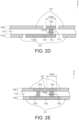
- FIG. 2D illustrates a schematic diagram of a cross-sectional view of the structure in FIG. 2C along a direction 2D-2D'
- FIG. 2E illustrates a schematic diagram of a cross-sectional view of the structure in FIG. 2C along a direction 2E-2E'.
- the first conductive layer 110 includes a first grounding net 111, at least one first signal ball-pad 112, at least one first signal via-pad 113, at least one first signal trace 114, at least one first grounding via-pad 115 and at least one first grounding ball-pad 116.
- the first grounding net 111 has a first ground void 1111. At least one the first signal ball-pad 112 is disposed within the first ground void 1111, where there is no conductive material existing in the void region to connect the signal pad and grounding net.
- the first signal ball-pad 112 has a first ball-pad diameter 112D
- the first ground void 1111 has a first ground void diameter 1111D, wherein a ratio of the first ground void diameter 1111D to the first ball-pad diameter 112D is equal to or greater than 1.2, for example.
- the capacitance between the first signal ball-pad 112 and the first grounding net 111 may be reduced for increasing the impedance.
- the differential impedance may be increased from 50 ohm ( ⁇ ) to 85 ⁇ , depending on the signal ball-pad dimensions.
- the first ground void diameter 1111D is a diameter of an approximate circle C1 as close to a lateral wall 1111W of the first ground void 1111 as possible.
- the approximate circle C1 surrounds the first signal ball-pad 112, and a circle center of the approximate circle C1 overlap a center 112C of the first signal ball-pad 112, for example.
- the first signal ball-pad 112 is spaced from a lateral wall 111 1W of the first ground void 1111 by a first minimum interval ⁇ d1, and the first minimum interval ⁇ d1 is greater than 0.1 times of the first ball-pad diameter 112D (that is, ⁇ d1 ⁇ 0.1 ⁇ 112D).
- the capacitance between the first signal ball-pad 112 and the first grounding net 111 may be reduced for increasing the impedance.
- Z diff is the differential impedance
- C S is a self-capacitance
- C m is a mutual capacitance
- L S is a self-inductance
- L m is a mutual inductance.
- the differential impedance Z diff is proportional to the capacitance. In other words, when the capacitance between the first signal ball-pad 112 and the first grounding net 111 reduces, the impedance is increased. Through the ratio design of the conductive layer in the present embodiment, it may achieve the continuous impedance with less reflection.
- Z diff 2 ⁇ L S ⁇ L m C S ⁇ C m
- the first conductive layer 110 is, for example, the bottom conductive layer (for example, the bottommost conductive layer) of the semiconductor device 100.
- the first signal ball-pad 112 may be exposed from the semiconductor device 100 for connecting a signal contact, for example, a solder ball, solder paste, a bump, a pillar, etc.
- the first signal via-pad 113, the first signal trace 114 and a second signal ball-pad 112A may be disposed within the first void 1111, wherein the first signal trace 114 connects the second signal ball-pad 112A with the first signal via-pad 113.
- the first grounding via-pad 115 may connect a grounding via (not illustrated in FIG. 2A ).
- the first grounding ball-pad 116 may be exposed from the semiconductor device 100 for connecting a grounding contact, for example, a solder ball, solder paste, a bump, a pillar, etc.
- the first signal via-pad 113 has a first via-pad diameter 113D
- the first ground void 1111 has a second ground void diameter 1112D, wherein a ratio of the second ground void diameter 1112D to the first via-pad diameter 113D is equal to or greater than 1.2, for example.
- the capacitance between the first signal via-pad 113 and the first grounding net 111 may be reduced for increasing the impedance.
- the first and second signal ball-pads 112 and 112A, the first signal via-pad 113 and the first signal trace 114 may be for used as signal transmission set or signal receiving set.
- the first conductive layer 110 may include at least one signal transmission set and/or at least one signal receiving set.
- the second conductive layer 120 is disposed above the first conductive layer 110.
- the second conductive layer 120 includes a second grounding net 121, at least one second signal via-pad 122 and at least one second grounding via-pad 123.
- the second grounding net 121 has a second ground void 1211, wherein the second signal via-pad 122 is disposed within the second ground void 1211.
- the second ground void 1211 has a third ground void diameter 1211D
- the second signal via-pad 122 has a second via-pad diameter 122D
- a ratio of the third ground void diameter 1211D to the second via-pad diameter 122D is equal to or greater than 1.2, for example.
- the capacitance between the second grounding net 121 and the second signal via-pad 122 may reduce for increasing the impedance.
- the second via-pad diameter 122D is a diameter of an approximate circle C2 as close to a lateral wall 1211W of the second ground void 1211 as possible.
- the approximate circle C2 surrounds the second signal via-pad 122, and a circle center of the approximate circle C2 overlap a center 122C of the second signal via-pad 122, for example.
- the second signal via-pad 122 is spaced from the lateral wall 1211W of the second ground void 1211 by a second minimum interval ⁇ d2, and the second minimum interval ⁇ d2 is greater than 0.1 times of the second via-pad diameter 122D (that is, ⁇ d2 ⁇ 0.1 ⁇ 122D).
- the capacitance between the second signal via-pad 122 and the second grounding net 121 may be reduced for increasing the impedance.
- a ratio of the third ground void diameter 1211D (as illustrated in FIG. 2B ) of the second ground void 1211 in the second conductive layer 120 to the first ball-pad diameter 112D (as illustrated in FIG. 2A ) of the first signal ball-pad 112 in the first conductive layer 110 may be greater than 1.0.
- the first ball-pad diameter 112D would be 280 ⁇ m or 240 ⁇ m.
- the second via-pad diameter 122D would be 50 ⁇ m, 80 ⁇ m, 100 ⁇ m, or 120 ⁇ m depending on the dimension of semiconductor device.
- the second conductive layer 120 may be disposed above the first conductive layer 110. Two adjacent conductive layers may be separated by a dielectric layer. For example, the second conductive layer 120 and the first conductive layer 110 may be separated by a dielectric layer 115.
- the second conductive layer 120 may be electrically connected with the first conductive layer 110 by at least one signal via 117. Furthermore, the signal via 117 connects the second signal via-pad 122 in the second conductive layer 120 with the first signal via-pad 113 in the first conductive layer 110.
- the signal via 117 has a via diameter 117D, and a ratio of the via diameter 117D to the second via-pad diameter 122D may equal to 0.5, even less or greater.
- the via diameter 117D is, for example, 50 micrometers ( ⁇ m)
- the second via-pad diameter 122D is, for example, 100 ⁇ m.
- the first ball-pad diameter 112D is greater than the second via-pad diameter 122D.
- the first signal ball-pad 112 may provide a larger area for receiving the signal contact, for example, a solder ball, solder paste, a bump, a pillar, etc.
- the second conductive layer 120 may be electrically connected with the first conductive layer 110 by at least one grounding via 118. Furthermore, the grounding via 118 connects the second grounding via-pad 123 in the second conductive layer 120 with the first grounding ball-pad 116 in the first conductive layer 110.
- the grounding via 118 has a via diameter 118D
- the second grounding ball-pad 123 has a second pad diameter 123D, wherein a ratio of the via diameter 118D to the second pad diameter 123D may equal to 0.5, even less or greater.
- the via diameter 118D is, for example, 50 micrometers ( ⁇ m)
- the second pad diameter 123D is, for example, 100 ⁇ m.
- At least one portion of the second ground void 1211 overlap at least one portion of the first signal ball-pad 112 in Z-axis, and accordingly it may reduce the capacitance for increasing the impedance.
- FIG. 3 illustrates a schematic diagram of a relationship between time vs. voltage of groups 1 to 5 in Table 1.
- the relationship between time vs. voltage may be obtained by using SBR (single-bit response) simulation.
- group 1 there are two conductive layers (Layer 3 and Layer 4) use the design of the ratio as started above, wherein a ground void diameter of at least one void in Layer 4 is 290 ⁇ m, and a ground void diameter of at least one void in Layer 3 is 240 ⁇ m.
- conductive layers there are three conductive layers (Layer 2, Layer 3 and Layer 4) use the design of the ratio as started above, wherein a ground void diameter of at least one void in Layer 4 is 290 ⁇ m, a ground void diameter of at least one void in Layer 3 is 290 ⁇ m, and a ground void diameter of at least one void in Layer 2 is 290 ⁇ m.
- conductive layers there are four conductive layers (Layer 1, Layer 2, Layer 3 and Layer 4) use the design of the ratio as started above, wherein a ground void diameter of at least one void in Layer 4 is 290 ⁇ m, a ground void diameter of at least one void in Layer 3 is 290 ⁇ m, a ground void diameter of at least one void in Layer 2 is 290 ⁇ m and a ground void diameter of at least one void in Layer 1 is 290 ⁇ m.
- conductive layers there are four conductive layers (Layer 1, Layer 2, Layer 3 and Layer 4) use the design of the ratio as started above, wherein a ground void diameter of at least one void in Layer 4 is 340 ⁇ m, a ground void diameter of at least one void in Layer 3 is 290 ⁇ m, a ground void diameter of at least one void in Layer 2 is 290 ⁇ m and a ground void diameter of at least one void in Layer 1 is 290 ⁇ m.
- conductive layers there are four conductive layers (Layer 1, Layer 2, Layer 3 and Layer 4) use the design of the ratio as started above, wherein a ground void diameter of at least one void in Layer 4 is 390 ⁇ m, a ground void diameter of at least one void in Layer 3 is 290 ⁇ m, a ground void diameter of at least one void in Layer 2 is 290 ⁇ m and a ground void diameter of at least one void in Layer 1 is 290 ⁇ m.
- the Layer 4 in group 5 has the greater the ground void diameter than that of Layer 4 in group 4.
- the Layer 4 is, for example, the bottommost conductive layer of the semiconductor device, and Layers 4 to 1 are disposed in order from bottom to top.
- the curves G1 to G5 present the output voltage Vout from the first signal ball-pad 112 (for example, in Layer 4) in groups 1 to 5 respectively.
- the input pulsed voltage Vin is input to a contact (for example, bump) of a chip , through the trace and connecting to the signal ball-pad (not illustrated) which may be disposed outside the semiconductor device 100 or inside the semiconductor device 100.
- the input pulsed voltage Vin is 0.2 v with 42.8 picosecond (ps) of one unit interval (UI), 10 ps of rise time and 10 ps of fall time, for example.
- the first reflections of groups 1 to 5 are shown in an enlarged diagram of FIG. 3 .
- the curve G5 presents the minimum signal reflection
- the curve G1 presents the maximum signal reflection.
- a ratio of the curve G1 to the curve G5 in 1 st reflection is -37.7 % (for example, calculation formula: 1 ⁇ ⁇ 24.7 ⁇ ⁇ 15.4 mV ⁇ 24.7 mV . It can be seen that the impedance continuity may be obviously improved by the size or ration design of the ground void and the signal ball-pad as stated above.
- FIG. 4 illustrates a schematic diagram of a first conductive layer 210 according to another embodiment of the present disclosure.
- the first conductive layer 210 may replace the first conductive layer 110 in FIG. 2A .
- the first conductive layer 210 includes a first grounding net 211, at least one first signal ball-pad 112, at least one first signal via-pad 113, at least one first signal trace 114, at least one first grounding via-pad 115 and at least one first grounding ball-pad 116.
- the first grounding net 211 has a boundary 211e, wherein the first void 2111 extends to the boundary 211e to form an opening 211a. In the present embodiment, the opening 211a exposes one first signal ball-pad 112.
- first connection line L1 of the center 112Cof the first signal ball-pad 112 and a first edge 211a1 of the opening 211a There is a second connection line L2 of the center 112C of the first signal ball-pad 112 and a second edge 211a2 of the opening 211a, wherein an angle A1 included between the first connection line L1 and the second connection line L2 may be equal to or greater than 60 degrees.
- the first conductive layer 210 may reduce the capacitance for increasing the impedance (for example, the differential impedance). For example, the impedance may be increased from 68 ⁇ to 73 ⁇ .
- the first ground void 2111' exposes an opening 211a'.
- the opening 211a' exposes a plurality of the first signal ball-pad 112'.
- the first conductive layer 210 may reduce the capacitance for increasing the impedance (for example, the differential impedance).
- the impedance may be increased from 68 ⁇ to 73 ⁇ .
- first ground void 2111 having the opening 211a and the opening 211a' may be applied to the first grounding net 111 in FIG. 2A .
- FIG. 5 illustrates a schematic diagram of a top view of a semiconductor device 300 according to another embodiment of the present disclosure.
- the semiconductor device 300 includes a chip and a package, and the chip may be stacked to the package.
- the chip includes a plurality of grounding contacts 330G, a plurality of negative electrode contacts 330N and a plurality of positive electrode contacts 330P.
- One electrode contact 330N and the positive electrode contact 330P construct one electrode set E1.
- one electrode set E1 may be located between two grounding contacts 330G, and in another region, a plurality of the electrode sets E1 may be located between two grounding contacts 330G.
- the package includes a plurality of grounding contacts 340G, a plurality of negative electrode contacts 340N and a plurality of positive electrode contacts 340P, a plurality of grounding traces 350G, a plurality of negative electrode traces 350N and a plurality of positive electrode traces 350P.
- the grounding trace 350G connects the grounding contact 330G through the grounding contacts 340G.
- the negative electrode trace 350N connects the negative electrode contact 330N through the negative electrode contact 340N.
- the positive electrode trace 350P connects the positive electrode contact 330P through the positive electrode contact 340P.
- the trace may be a SerDes (Serializer/Deserializer) trace.
- the positive electrode contact 330P and the negative electrode contact 330N are staggered to each other in a first direction and a second direction different from the first direction, wherein the first direction is, for example, parallel to X-axis, and the second direction is, for example, parallel to Y-axis.
- the chip size can be reduced with the staggered electrode contacts.
- each trace has a trace width W1, and the trace widths W1 are substantially equal in the breakout region and out of breakout region as shown in FIG. 5 , for example.
- the substantially equal trace widths W1 and/or the substantially equal spaces S1 may achieve the continuous impedance with less reflection.
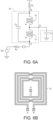
- FIG. 6A illustrates a schematic diagram of a T-coil circuit 10 according to an embodiment of the present disclosure
- FIG. 6B illustrates a schematic diagram of a coil 13 of the T-coil circuit 10 in FIG. 6A
- the T-coil circuit 10 may be disposed in the chip to counteract the effects of parasitic capacitances (C L ) including electrostatic discharge (ESD) protection circuits, input/output (I/O) pads, and others.
- C L parasitic capacitances
- ESD electrostatic discharge
- I/O input/output
- the T-coil circuit 10 includes a first inductor 11 and a second inductor 12, wherein a first inductance value L 1 of the first inductor 11 and a second inductance value L 2 of the second inductor 12 satisfy the following formulas (2a) to (2b).
- ⁇ is a damping factor of a transfer function
- C L is a load capacitance
- C B is a bridge capacitor
- R T is a termination resistance.
- C B C L 16 ⁇ 2
- a coil 13 forming the first inductor 11 and the second inductor 12 may spirally extend from a first terminal A to a second terminal B, wherein a third terminal D connects a line between the first inductor 11 and the second inductor 12 with the load capacitance C L .
- the T-coil circuit 10 is a special form of an inductive peaking circuit that will extend an amplifier's bandwidth and speed up the output signal rise-time.
- the circuit uses a coupled inductor and a small bridging capacitor.
- the T-coil circuit 10 may double the bandwidth of an amplifier.
- the inductor as steers an input current into the load capacitance C L , so it charges up more rapidly.
- the small bridging capacitor ensures that the input impedance of the T-coil is constant and resistive.
- the impedance Z in is equal to a termination resistance R T
- the inductance value of the coil 13 is proportional to value of R T 2 (or proportional to the impedance Z in ).
- R T Z in ( ⁇ ) R T 2 L (nH) ratio 60.0 3,600 1.44 44% 50.0 2,500 1.00 0 45.0 2,025 0.81 -19% 42.5 1,806 0.72 -28% 40.0 1,600 0.64 -36% 37.5 1,406 0.56 -44% 35.0 1,225 0.49 -51%
- FIG. 7 illustrates a schematic diagram of a T-coil circuit 20 according to another embodiment of the present disclosure.
- the T-coil circuit 20 may be disposed in or on a chip, a silicon interposer, a substrate, a package or a circuit board.
- the T-coil circuit 20 includes a first coil 21A, a second coil 21B, a third coil 21C and a fourth coil 21D, a first conductive trace set 22A, a second conductive trace set 22B, a third conductive trace set 22C and a fourth conductive trace set 22D.
- the first conductive trace set 22A includes a first trace 22A1 and a second trace 22A2, and the first trace 22A1 and the second trace 22A2 are connected with two terminal of the first coil 21A.
- the second conductive trace set 22B includes a first trace 22B1 and a second trace 22B2, and the first trace 22B1 and the second trace 22B2 are connected with two terminal of the second coil 21B.
- the third conductive trace set 22C includes a first trace 22C1 and a second trace 22C2, and the first trace 22C1 and the second trace 22C2 are connected with two terminal of the third coil 21C.
- the fourth conductive trace set 22D includes a first trace 22D1 and a second trace 22D2, and the first trace 22D1 and the second trace 22D2 are connected with two terminal of the fourth coil 21D.
- the first conductive trace set 22A may be electrically connected with the first coil 21A through a first controller (not illustrated).
- the second conductive trace set 22B may be electrically connected with the second coil 21B through a second controller (not illustrated).
- the third conductive trace set 22C may be electrically connected with the third coil 21C through a third controller (not illustrated).
- the fourth conductive trace set 22D may be electrically connected with the fourth coil 21D through a fourth controller (not illustrated).
- the first controller, the second controller, the third controller and the fourth controller include, for example, MUX/Selector or MOS switch.
- the segmented spiral inductors in the T-coil network would be selected through at least one controller (including, for example, MUX/Selector or MOS switch) to match the dedicated termination (R T ) or compensate the process variation.
- at least one controller including, for example, MUX/Selector or MOS switch
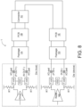
- FIG. 8 illustrates a schematic diagram of a semiconductor system 1 according to another embodiment of the present disclosure.
- the semiconductor system 1 includes a package 1A, a package 1B, a connector 1C, a PCB 1D, a PCB 1E, a driver and a receiver.
- the driver may transmit a signal to the receiver through the T-coil, the package 1A, the PCB 1B, the connector 1C, the PCB 1E, the package 1D and the T-coil.
- the ESD component is equivalent to a larger capacitor, and the T-coil is electrically connected with the ESD component and may provide a inductance for impedance matching.
- the aforementioned ratio design of the conductive layer may be applied to the package 1A, the PCB 1B, the package 1D, the PCB 1E, etc.
- the embodiment of the present invention provides a semiconductor device.
- the semiconductor device includes at least two conductive layers, wherein at least one of the conductive layers includes a grounding net and at least one signal ball-pad, and the grounding net has at least one ground void in the signal ball-pad is disposed.
- the signal ball-pad has a ball-pad diameter
- the ground void has a ground void diameter
- a ratio of the ground void diameter to the ball-pad diameter is equal to or greater than 1.2.
Landscapes
- Engineering & Computer Science (AREA)
- Microelectronics & Electronic Packaging (AREA)
- Power Engineering (AREA)
- Semiconductor Integrated Circuits (AREA)
- Internal Circuitry In Semiconductor Integrated Circuit Devices (AREA)
- Physics & Mathematics (AREA)
- Geometry (AREA)
Abstract
Description
- The invention relates in general to a semiconductor device.
- Interfaces with discontinuous impedances will produce signal reflections. The impedance mismatch will lead to signal reflection and attenuation, which is manifested in reverse signal transmission, signal attenuation, and signal distortion. If there is an impedance mismatch at one end of the transmission line, part of the signal will be reflected back. This will affect the power transfer and signal quality of the signal in the transmission line, and also cause echo interference.
- According to an embodiment of the present disclosure, a semiconductor device is provided. The semiconductor device includes a first conductive layer and second conductive layer. The second conductive layer is disposed opposite to the first conductive layer. One of the first conductive layer and the second conductive layer includes a first grounding net and a first signal ball-pad. The first grounding net has a first void, and the first signal ball-pad is disposed in the first void. The first signal ball-pad has a first pad diameter, the first void has a first ground void diameter, and a ratio of the first ground void diameter to the first pad diameter is equal to or greater than 1.2.
- According to another embodiment of the present disclosure, a semiconductor device is provided. The semiconductor device includes a first conductive layer and second conductive layer. The second conductive layer is disposed opposite to the first conductive layer. One of the first conductive layer and the second conductive layer includes a first grounding net and a first signal ball-pad. The first signal ball-pad has a first ball-pad diameter, the first signal ball-pad is spaced from a lateral wall of the first void by a first minimum interval, and the first minimum interval is greater than 0.1 times of the first ball-pad diameter.
- The above and other aspects of the disclosure will become better understood with regard to the following detailed description of the preferred but non-limiting embodiment (s). The following description is made with reference to the accompanying drawings.
-
-
FIG. 1 illustrates a schematic diagram of a semiconductor device according to an embodiment of the present disclosure; -
FIG. 2A illustrates a schematic diagram of a first conductive layer of the semiconductor device inFIG. 1 ; -
FIG. 2B illustrates a schematic diagram of a second conductive layer of the semiconductor device inFIG. 1 ; -
FIG. 2C illustrates a schematic diagram of the first conductive layer inFIG. 2A and the second conductive layer inFIG. 2B overlapping; -
FIG. 2D illustrates a schematic diagram of a cross-sectional view of the structure inFIG. 2C along adirection 2D-2D'; -
FIG. 2E illustrates a schematic diagram of a cross-sectional view of the structure inFIG. 2C along adirection 2E-2E'; -
FIG. 3 illustrates a schematic diagram of a relationship between time vs. voltage ofgroups 1 to 5 in Table 1; -
FIG. 4 illustrates a schematic diagram of a first conductive layer according to another embodiment of the present disclosure; -
FIG. 5 illustrates a schematic diagram of a top view of asemiconductor device 300 according to another embodiment of the present disclosure; -
FIG. 6A illustrates a schematic diagram of a T-coil circuit according to an embodiment of the present disclosure; -
FIG. 6B illustrates a schematic diagram of a coil of the T-coil circuit inFIG. 6A ; -
FIG. 7 illustrates a schematic diagram of a T-coil circuit 20 according to another embodiment of the present disclosure; and -
FIG. 8 illustrates a schematic diagram of asemiconductor system 1 according to another embodiment of the present disclosure. - Referring to
FIG. 1, FIG. 1 illustrates a schematic diagram of asemiconductor device 100 according to an embodiment of the present disclosure. Thesemiconductor device 100 is, for example, a semiconductor chip, a silicon interposer, a substrate, a semiconductor package, a circuit board (for example, a printed circuit board), etc. Thesemiconductor device 100 includes at least one conductive layer, wherein the conductive layer may reduce a capacitance for increasing an impedance (for example, a differential impedance). For example, the differential impedance may be increased from 50 ohm (Ω) to 85 Ω, depending on the signal ball-pad dimensions. - Referring to
FIGS. 2A to 2E ,FIG. 2A illustrates a schematic diagram of a first conductive layer of thesemiconductor device 100 inFIG. 1 ,FIG. 2B illustrates a schematic diagram of a second conductive layer of thesemiconductor device 100 inFIG. 1 ,FIG. 2C illustrates a schematic diagram of the firstconductive layer 110 inFIG. 2A and the secondconductive layer 120 inFIG. 2B overlapping,FIG. 2D illustrates a schematic diagram of a cross-sectional view of the structure inFIG. 2C along adirection 2D-2D', andFIG. 2E illustrates a schematic diagram of a cross-sectional view of the structure inFIG. 2C along adirection 2E-2E'. - As illustrated in
FIG. 2A , the firstconductive layer 110 includes afirst grounding net 111, at least one first signal ball-pad 112, at least one first signal via-pad 113, at least onefirst signal trace 114, at least one first grounding via-pad 115 and at least one first grounding ball-pad 116. - As illustrated in
FIG. 2A , thefirst grounding net 111 has afirst ground void 1111. At least one the first signal ball-pad 112 is disposed within thefirst ground void 1111, where there is no conductive material existing in the void region to connect the signal pad and grounding net. The first signal ball-pad 112 has a first ball-pad diameter 112D, and thefirst ground void 1111 has a first groundvoid diameter 1111D, wherein a ratio of the first groundvoid diameter 1111D to the first ball-pad diameter 112D is equal to or greater than 1.2, for example. As a result, the capacitance between the first signal ball-pad 112 and thefirst grounding net 111 may be reduced for increasing the impedance. For example, the differential impedance may be increased from 50 ohm (Ω) to 85 Ω , depending on the signal ball-pad dimensions. The first groundvoid diameter 1111D is a diameter of an approximate circle C1 as close to alateral wall 1111W of thefirst ground void 1111 as possible. The approximate circle C1 surrounds the first signal ball-pad 112, and a circle center of the approximate circle C1 overlap acenter 112C of the first signal ball-pad 112, for example. - In an embodiment, the first signal ball-
pad 112 is spaced from alateral wall 111 1W of thefirst ground void 1111 by a first minimum interval Δd1, and the first minimum interval Δd1 is greater than 0.1 times of the first ball-pad diameter 112D (that is, Δd1 ≥ 0.1 × 112D). As a result, the capacitance between the first signal ball-pad 112 and thefirst grounding net 111 may be reduced for increasing the impedance. - As shown in formula (1) below, Zdiff is the differential impedance, CS is a self-capacitance, Cm is a mutual capacitance, LS is a self-inductance, and Lm is a mutual inductance. According to formula (1), the differential impedance Zdiff is proportional to the capacitance. In other words, when the capacitance between the first signal ball-
pad 112 and thefirst grounding net 111 reduces, the impedance is increased. Through the ratio design of the conductive layer in the present embodiment, it may achieve the continuous impedance with less reflection.
- As illustrated in
FIG. 2A , the firstconductive layer 110 is, for example, the bottom conductive layer (for example, the bottommost conductive layer) of thesemiconductor device 100. The first signal ball-pad 112 may be exposed from thesemiconductor device 100 for connecting a signal contact, for example, a solder ball, solder paste, a bump, a pillar, etc. The first signal via-pad 113, thefirst signal trace 114 and a second signal ball-pad 112A may be disposed within thefirst void 1111, wherein thefirst signal trace 114 connects the second signal ball-pad 112A with the first signal via-pad 113. The first grounding via-pad 115 may connect a grounding via (not illustrated inFIG. 2A ). The first grounding ball-pad 116 may be exposed from thesemiconductor device 100 for connecting a grounding contact, for example, a solder ball, solder paste, a bump, a pillar, etc. The first signal via-pad 113 has a first via-pad diameter 113D, and thefirst ground void 1111 has a second groundvoid diameter 1112D, wherein a ratio of the second groundvoid diameter 1112D to the first via-pad diameter 113D is equal to or greater than 1.2, for example. As a result, the capacitance between the first signal via-pad 113 and thefirst grounding net 111 may be reduced for increasing the impedance. - In an embodiment, the first and second signal ball-
pads pad 113 and thefirst signal trace 114 may be for used as signal transmission set or signal receiving set. In an embodiment, the firstconductive layer 110 may include at least one signal transmission set and/or at least one signal receiving set. - As illustrated in
FIG. 2B , in an embodiment, the secondconductive layer 120 is disposed above the firstconductive layer 110. The secondconductive layer 120 includes asecond grounding net 121, at least one second signal via-pad 122 and at least one second grounding via-pad 123. - As illustrated in
FIG. 2B , thesecond grounding net 121 has asecond ground void 1211, wherein the second signal via-pad 122 is disposed within thesecond ground void 1211. Thesecond ground void 1211 has a third groundvoid diameter 1211D, the second signal via-pad 122 has a second via-pad diameter 122D, and a ratio of the third groundvoid diameter 1211D to the second via-pad diameter 122D is equal to or greater than 1.2, for example. As a result, the capacitance between thesecond grounding net 121 and the second signal via-pad 122 may reduce for increasing the impedance. The second via-pad diameter 122D is a diameter of an approximate circle C2 as close to alateral wall 1211W of thesecond ground void 1211 as possible. The approximate circle C2 surrounds the second signal via-pad 122, and a circle center of the approximate circle C2 overlap acenter 122C of the second signal via-pad 122, for example. - In an embodiment, the second signal via-
pad 122 is spaced from thelateral wall 1211W of thesecond ground void 1211 by a second minimum interval Δd2, and the second minimum interval Δd2 is greater than 0.1 times of the second via-pad diameter 122D (that is, Δd2 ≥ 0.1 × 122D). As a result, the capacitance between the second signal via-pad 122 and thesecond grounding net 121 may be reduced for increasing the impedance. - In an embodiment, a ratio of the third ground
void diameter 1211D (as illustrated inFIG. 2B ) of thesecond ground void 1211 in the secondconductive layer 120 to the first ball-pad diameter 112D (as illustrated inFIG. 2A ) of the first signal ball-pad 112 in the firstconductive layer 110 may be greater than 1.0. For example, the first ball-pad diameter 112D would be 280 µm or 240 µm. The second via-pad diameter 122D would be 50 µm, 80 µm, 100 µm, or 120 µm depending on the dimension of semiconductor device. - As illustrated in
FIGS. 2C and2D , the secondconductive layer 120 may be disposed above the firstconductive layer 110. Two adjacent conductive layers may be separated by a dielectric layer. For example, the secondconductive layer 120 and the firstconductive layer 110 may be separated by adielectric layer 115. The secondconductive layer 120 may be electrically connected with the firstconductive layer 110 by at least one signal via 117. Furthermore, the signal via 117 connects the second signal via-pad 122 in the secondconductive layer 120 with the first signal via-pad 113 in the firstconductive layer 110. The signal via 117 has a viadiameter 117D, and a ratio of the viadiameter 117D to the second via-pad diameter 122D may equal to 0.5, even less or greater. For example, the viadiameter 117D is, for example, 50 micrometers (µm), and the second via-pad diameter 122D is, for example, 100 µm. - As illustrated in
FIGS. 2B and2C , the first ball-pad diameter 112D is greater than the second via-pad diameter 122D. As a result, the first signal ball-pad 112 may provide a larger area for receiving the signal contact, for example, a solder ball, solder paste, a bump, a pillar, etc. - As illustrated in
FIGS. 2C and2E , the secondconductive layer 120 may be electrically connected with the firstconductive layer 110 by at least one grounding via 118. Furthermore, the grounding via 118 connects the second grounding via-pad 123 in the secondconductive layer 120 with the first grounding ball-pad 116 in the firstconductive layer 110. The grounding via 118 has a viadiameter 118D, and the second grounding ball-pad 123 has asecond pad diameter 123D, wherein a ratio of the viadiameter 118D to thesecond pad diameter 123D may equal to 0.5, even less or greater. For example, the viadiameter 118D is, for example, 50 micrometers (µm), and thesecond pad diameter 123D is, for example, 100 µm. - As illustrated in
FIG. 2C , in an embodiment, at least one portion of thesecond ground void 1211 overlap at least one portion of the first signal ball-pad 112 in Z-axis, and accordingly it may reduce the capacitance for increasing the impedance. - Referring to
FIG. 3, FIG. 3 illustrates a schematic diagram of a relationship between time vs. voltage ofgroups 1 to 5 in Table 1. The relationship between time vs. voltage may be obtained by using SBR (single-bit response) simulation. Ingroup 1, there are two conductive layers (Layer 3 and Layer 4) use the design of the ratio as started above, wherein a ground void diameter of at least one void in Layer 4 is 290 µm, and a ground void diameter of at least one void in Layer 3 is 240 µm. In group 2, there are three conductive layers (Layer 2, Layer 3 and Layer 4) use the design of the ratio as started above, wherein a ground void diameter of at least one void in Layer 4 is 290 µm, a ground void diameter of at least one void in Layer 3 is 290 µm, and a ground void diameter of at least one void in Layer 2 is 290 µm. In group 3, there are four conductive layers (Layer 1, Layer 2, Layer 3 and Layer 4) use the design of the ratio as started above, wherein a ground void diameter of at least one void in Layer 4 is 290 µm, a ground void diameter of at least one void in Layer 3 is 290 µm, a ground void diameter of at least one void in Layer 2 is 290 µm and a ground void diameter of at least one void inLayer 1 is 290 µm. In group 4, there are four conductive layers (Layer 1, Layer 2, Layer 3 and Layer 4) use the design of the ratio as started above, wherein a ground void diameter of at least one void in Layer 4 is 340 µm, a ground void diameter of at least one void in Layer 3 is 290 µm, a ground void diameter of at least one void in Layer 2 is 290 µm and a ground void diameter of at least one void inLayer 1 is 290 µm. In group 5, there are four conductive layers (Layer 1, Layer 2, Layer 3 and Layer 4) use the design of the ratio as started above, wherein a ground void diameter of at least one void in Layer 4 is 390 µm, a ground void diameter of at least one void in Layer 3 is 290 µm, a ground void diameter of at least one void in Layer 2 is 290 µm and a ground void diameter of at least one void inLayer 1 is 290 µm. The Layer 4 in group 5 has the greater the ground void diameter than that of Layer 4 in group 4. The Layer 4 is, for example, the bottommost conductive layer of the semiconductor device, and Layers 4 to 1 are disposed in order from bottom to top.
- As illustrated in
FIG. 3 , the curves G1 to G5 present the output voltage Vout from the first signal ball-pad 112 (for example, in Layer 4) ingroups 1 to 5 respectively. The input pulsed voltage Vin is input to a contact (for example, bump) of a chip , through the trace and connecting to the signal ball-pad (not illustrated) which may be disposed outside thesemiconductor device 100 or inside thesemiconductor device 100. The input pulsed voltage Vin is 0.2 v with 42.8 picosecond (ps) of one unit interval (UI), 10 ps of rise time and 10 ps of fall time, for example. The first reflections ofgroups 1 to 5 are shown in an enlarged diagram ofFIG. 3 . - As illustrated in
FIG. 3 , the less the signal reflection, the better the impedance continuity is. The curve G5 presents the minimum signal reflection, and the curve G1 presents the maximum signal reflection. A ratio of the curve G1 to the curve G5 in 1st reflection is -37.7 % (for example, calculation formula:
- Referring to
FIG. 4, FIG. 4 illustrates a schematic diagram of a firstconductive layer 210 according to another embodiment of the present disclosure. The firstconductive layer 210 may replace the firstconductive layer 110 inFIG. 2A . The firstconductive layer 210 includes afirst grounding net 211, at least one first signal ball-pad 112, at least one first signal via-pad 113, at least onefirst signal trace 114, at least one first grounding via-pad 115 and at least one first grounding ball-pad 116. Thefirst grounding net 211 has aboundary 211e, wherein thefirst void 2111 extends to theboundary 211e to form anopening 211a. In the present embodiment, theopening 211a exposes one first signal ball-pad 112. There is a first connection line L1 of the center 112Cof the first signal ball-pad 112 and a first edge 211a1 of theopening 211a, and There is a second connection line L2 of thecenter 112C of the first signal ball-pad 112 and a second edge 211a2 of theopening 211a, wherein an angle A1 included between the first connection line L1 and the second connection line L2 may be equal to or greater than 60 degrees. As a result, the firstconductive layer 210 may reduce the capacitance for increasing the impedance (for example, the differential impedance). For example, the impedance may be increased from 68 Ω to 73 Ω. - As illustrated in
FIG. 4 , the first ground void 2111' exposes anopening 211a'. In the present embodiment, theopening 211a' exposes a plurality of the first signal ball-pad 112'. There is a first connection line L1' of the center 1120' of the first signal ball-pad 112' and a first edge 211a1' of theopening 211a', and there is a second connection line L2' of the center 1120' of the first signal ball-pad 112' and a second edge 211a2' of theopening 211a', wherein an angle A1' included between the first connection line L1' and the second connection line L2' may be equal to or greater than 60 degrees. As a result, the firstconductive layer 210 may reduce the capacitance for increasing the impedance (for example, the differential impedance). For example, the impedance may be increased from 68 Ω to 73 Ω. - In another embodiment, the
first ground void 2111 having theopening 211a and theopening 211a' may be applied to thefirst grounding net 111 inFIG. 2A . - Referring to
FIG. 5, FIG. 5 illustrates a schematic diagram of a top view of asemiconductor device 300 according to another embodiment of the present disclosure. Thesemiconductor device 300 includes a chip and a package, and the chip may be stacked to the package. - As illustrated in
FIG. 5 , the chip includes a plurality ofgrounding contacts 330G, a plurality ofnegative electrode contacts 330N and a plurality ofpositive electrode contacts 330P. Oneelectrode contact 330N and thepositive electrode contact 330P construct one electrode set E1. In an embodiment, in a region, one electrode set E1 may be located between two groundingcontacts 330G, and in another region, a plurality of the electrode sets E1 may be located between two groundingcontacts 330G. - As illustrated in
FIG. 5 , the package includes a plurality ofgrounding contacts 340G, a plurality ofnegative electrode contacts 340N and a plurality ofpositive electrode contacts 340P, a plurality of grounding traces 350G, a plurality of negative electrode traces 350N and a plurality of positive electrode traces 350P. - As illustrated in
FIG. 5 , thegrounding trace 350G connects thegrounding contact 330G through thegrounding contacts 340G. Thenegative electrode trace 350N connects thenegative electrode contact 330N through thenegative electrode contact 340N. Thepositive electrode trace 350P connects thepositive electrode contact 330P through thepositive electrode contact 340P. In an embodiment, the trace may be a SerDes (Serializer/Deserializer) trace. - As illustrated in
FIG. 5 , in the present embodiment, thepositive electrode contact 330P and thenegative electrode contact 330N are staggered to each other in a first direction and a second direction different from the first direction, wherein the first direction is, for example, parallel to X-axis, and the second direction is, for example, parallel to Y-axis. As a result, the chip size can be reduced with the staggered electrode contacts. - As illustrated in
FIG. 5 , each trace has a trace width W1, and the trace widths W1 are substantially equal in the breakout region and out of breakout region as shown inFIG. 5 , for example. There is a trace space S1 between two adjacent traces, wherein the trace spaces S1 are substantially equal, for example. The substantially equal trace widths W1 and/or the substantially equal spaces S1 may achieve the continuous impedance with less reflection. - Referring to
FIGS. 6A and 6B, FIG. 6A illustrates a schematic diagram of a T-coil circuit 10 according to an embodiment of the present disclosure, andFIG. 6B illustrates a schematic diagram of acoil 13 of the T-coil circuit 10 inFIG. 6A . The T-coil circuit 10 may be disposed in the chip to counteract the effects of parasitic capacitances (CL) including electrostatic discharge (ESD) protection circuits, input/output (I/O) pads, and others. - As illustrated in
FIG. 6A , the T-coil circuit 10 includes afirst inductor 11 and asecond inductor 12, wherein a first inductance value L1 of thefirst inductor 11 and a second inductance value L2 of thesecond inductor 12 satisfy the following formulas (2a) to (2b). In formulas (2a) to (2b), ζ is a damping factor of a transfer function, CL is a load capacitance, CB is a bridge capacitor, and RT is a termination resistance.

- As illustrated in
FIGS. 6A and 6B , acoil 13 forming thefirst inductor 11 and thesecond inductor 12 may spirally extend from a first terminal A to a second terminal B, wherein a third terminal D connects a line between thefirst inductor 11 and thesecond inductor 12 with the load capacitance CL. - The T-
coil circuit 10 is a special form of an inductive peaking circuit that will extend an amplifier's bandwidth and speed up the output signal rise-time. The circuit uses a coupled inductor and a small bridging capacitor. The T-coil circuit 10 may double the bandwidth of an amplifier. The inductor as steers an input current into the load capacitance CL, so it charges up more rapidly. The small bridging capacitor ensures that the input impedance of the T-coil is constant and resistive. - As shown in Table 2 below, the impedance Zin is equal to a termination resistance RT, and the inductance value of the
coil 13 is proportional to value of RT 2 (or proportional to the impedance Zin). The less the termination resistance RT is, the less the occupied area of thecoil 13 is. In other words, compared to the differential impedance (=2RT) being 100 Ω, the occupied area of thecoil 13 is less when the differential impedance (=2RT) being 80 Ω (for example, reduced by 36 %).Table 2 RT=Zin (Ω) RT 2 L (nH) ratio 60.0 3,600 1.44 44% 50.0 2,500 1.00 0 45.0 2,025 0.81 -19% 42.5 1,806 0.72 -28% 40.0 1,600 0.64 -36% 37.5 1,406 0.56 -44% 35.0 1,225 0.49 -51% - Referring to
FIG. 7, FIG. 7 illustrates a schematic diagram of a T-coil circuit 20 according to another embodiment of the present disclosure. The T-coil circuit 20 may be disposed in or on a chip, a silicon interposer, a substrate, a package or a circuit board. - As illustrated in
FIG. 7 , the T-coil circuit 20 includes afirst coil 21A, asecond coil 21B, athird coil 21C and afourth coil 21D, a first conductive trace set 22A, a second conductive trace set 22B, a third conductive trace set 22C and a fourth conductive trace set 22D. The first conductive trace set 22A includes a first trace 22A1 and a second trace 22A2, and the first trace 22A1 and the second trace 22A2 are connected with two terminal of thefirst coil 21A. The second conductive trace set 22B includes a first trace 22B1 and a second trace 22B2, and the first trace 22B1 and the second trace 22B2 are connected with two terminal of thesecond coil 21B. The third conductive trace set 22C includes a first trace 22C1 and a second trace 22C2, and the first trace 22C1 and the second trace 22C2 are connected with two terminal of thethird coil 21C. The fourth conductive trace set 22D includes a first trace 22D1 and a second trace 22D2, and the first trace 22D1 and the second trace 22D2 are connected with two terminal of thefourth coil 21D. - As illustrated in
FIG. 7 , the first conductive trace set 22A may be electrically connected with thefirst coil 21A through a first controller (not illustrated). The second conductive trace set 22B may be electrically connected with thesecond coil 21B through a second controller (not illustrated). The third conductive trace set 22C may be electrically connected with thethird coil 21C through a third controller (not illustrated). The fourth conductive trace set 22D may be electrically connected with thefourth coil 21D through a fourth controller (not illustrated). The first controller, the second controller, the third controller and the fourth controller include, for example, MUX/Selector or MOS switch. - In the present embodiment, like using at least one bond wire (not illustrated) to adjust spiral inductors (namely, the
first coil 21A, thesecond coil 21B, thethird coil 21C and thefourth coil 21D) in the package (for example, a BGA package), the segmented spiral inductors in the T-coil network would be selected through at least one controller (including, for example, MUX/Selector or MOS switch) to match the dedicated termination (RT) or compensate the process variation. - Referring to
FIG. 8, FIG. 8 illustrates a schematic diagram of asemiconductor system 1 according to another embodiment of the present disclosure. Thesemiconductor system 1 includes apackage 1A, apackage 1B, aconnector 1C, aPCB 1D, aPCB 1E, a driver and a receiver. The driver may transmit a signal to the receiver through the T-coil, thepackage 1A, thePCB 1B, theconnector 1C, thePCB 1E, thepackage 1D and the T-coil. The ESD component is equivalent to a larger capacitor, and the T-coil is electrically connected with the ESD component and may provide a inductance for impedance matching. In addition, the aforementioned ratio design of the conductive layer may be applied to thepackage 1A, thePCB 1B, thepackage 1D, thePCB 1E, etc. - In summary, the embodiment of the present invention provides a semiconductor device. The semiconductor device includes at least two conductive layers, wherein at least one of the conductive layers includes a grounding net and at least one signal ball-pad, and the grounding net has at least one ground void in the signal ball-pad is disposed. The signal ball-pad has a ball-pad diameter, the ground void has a ground void diameter, and a ratio of the ground void diameter to the ball-pad diameter is equal to or greater than 1.2. As a result, the capacitance between the signal ball-pad and the grounding net may be reduced for increasing the impedance and impedance continuity.
- While the disclosure has been described by way of example and in terms of the preferred embodiment (s), it is to be understood that the disclosure is not limited thereto. Based on the technical features embodiments of the present disclosure, a person ordinarily skilled in the art will be able to make various modifications and similar arrangements and procedures without breaching the scope of protection of the disclosure. Therefore, the scope of protection of the present disclosure should be accorded with what is defined in the appended claims.
Claims (9)
- A semiconductor device (100), characterized in that the semiconductor device (100) comprises:a first conductive layer (110, 210), anda second conductive layer (120) disposed opposite to the first conductive layer (110, 210);wherein the first conductive layer (110, 210) comprises:a first grounding net (111, 211) having a first ground void (1111, 2111, 2111'); anda first signal ball-pad (112, 112') in the first ground void (1111, 2111, 2111');wherein the first signal ball-pad (112, 112') has a first ball-pad diameter (112D), the first ground void (1111, 2111, 2111') has a first ground void diameter, and a ratio of the first ground void diameter to the first ball-pad diameter (112D) is equal to or greater than 1.2.
- The semiconductor device according to claim 1, characterized in that the first conductive layer (110, 210) is a bottom layer, the first signal ball-pad (112, 112') of the bottom layer is configured for connecting a contact.
- The semiconductor device according to claim 1 or claim 2, characterized in that the first conductive layer (110, 210) comprises:
a first signal via-pad (113) within the first ground void (1111, 2111, 2111');
wherein the first ground void (1111, 2111, 2111') has a second ground void diameter (1112D), the first signal via-pad (113) has a first via-pad diameter (113D), and a ratio of the second ground void diameter (1112D) to the first via-pad diameter (113D) is equal to or greater than 1.2. - The semiconductor device according to any one of the preceding claims, characterized in that the second conductive layer (120) is disposed above the first conductive layer (110, 210), the second conductive layer (120) comprises:a second grounding net (121) having a second ground void (1211); anda second signal via-pad (122) within the second ground void (1211);wherein the second ground void (1211) has a third ground void diameter (1211D), the second signal via-pad (122) has a second via-pad diameter (122D), and a ratio of the third ground void diameter (1211D) to the second via-pad diameter (122D) is equal to or greater than 1.2.
- The semiconductor device according to claim 3, characterized in that the first ball-pad diameter (112D) is greater than the first via-pad diameter (113D).
- The semiconductor device according to claim 4, characterized in that the first signal ball-pad (112, 112') at least partially overlaps the second ground void (1211) in a stack direction of the first conductive layer (110, 210) and the second conductive layer (120).
- The semiconductor device according to claim 4 or claim 5, characterized in that the second ground void diameter (1112D) is greater than the first ball-pad diameter (112D).
- The semiconductor device according to any one of the preceding claims, characterized in that the first grounding net (111, 211) has a boundary (211e), the first ground void (1111, 2111, 2111') extends to the boundary (211e) to form an opening (211a, 211a'), and the opening (211a, 211a') exposes the first signal ball-pad (112, 112').
- The semiconductor device according to claim 8, characterized in that there is a first connection line (L1, L1') of a center (112C, 112C') of the first signal ball-pad (112, 112') and a first edge (211a1, 211a1') of the opening (211a, 211a'), and there is a second connection line (L2, L2') of the center (112C, 112C') of the first signal ball-pad (112, 112') and a second edge (211a2, 211a2') of the opening (211a, 211a'), wherein an angle (A1, A1') included between the first connection line (L1, L1') and the second connection line (L2, L2') is equal to or greater than 60 degrees.
Applications Claiming Priority (1)
| Application Number | Priority Date | Filing Date | Title |
|---|---|---|---|
| US202363584515P | 2023-09-22 | 2023-09-22 |
Publications (1)
| Publication Number | Publication Date |
|---|---|
| EP4528814A1 true EP4528814A1 (en) | 2025-03-26 |
Family
ID=92895803
Family Applications (1)
| Application Number | Title | Priority Date | Filing Date |
|---|---|---|---|
| EP24201899.2A Pending EP4528814A1 (en) | 2023-09-22 | 2024-09-23 | Semiconductor device |
Country Status (4)
| Country | Link |
|---|---|
| US (1) | US20250105111A1 (en) |
| EP (1) | EP4528814A1 (en) |
| CN (1) | CN119695036A (en) |
| TW (1) | TW202514995A (en) |
Citations (4)
| Publication number | Priority date | Publication date | Assignee | Title |
|---|---|---|---|---|
| US20110248800A1 (en) * | 2008-12-25 | 2011-10-13 | Taras Kushta | Filter based on a combined via structure |
| US20160013536A1 (en) * | 2012-03-09 | 2016-01-14 | Finisar Corporation | 3-d integrated package |
| US20170179050A1 (en) * | 2015-12-18 | 2017-06-22 | Renesas Electronics Corporation | Semiconductor device |
| US20230170290A1 (en) * | 2021-11-26 | 2023-06-01 | Samsung Electronics Co., Ltd. | Semiconductor package |
-
2024
- 2024-09-23 TW TW113136013A patent/TW202514995A/en unknown
- 2024-09-23 US US18/892,608 patent/US20250105111A1/en active Pending
- 2024-09-23 CN CN202411326815.9A patent/CN119695036A/en active Pending
- 2024-09-23 EP EP24201899.2A patent/EP4528814A1/en active Pending
Patent Citations (4)
| Publication number | Priority date | Publication date | Assignee | Title |
|---|---|---|---|---|
| US20110248800A1 (en) * | 2008-12-25 | 2011-10-13 | Taras Kushta | Filter based on a combined via structure |
| US20160013536A1 (en) * | 2012-03-09 | 2016-01-14 | Finisar Corporation | 3-d integrated package |
| US20170179050A1 (en) * | 2015-12-18 | 2017-06-22 | Renesas Electronics Corporation | Semiconductor device |
| US20230170290A1 (en) * | 2021-11-26 | 2023-06-01 | Samsung Electronics Co., Ltd. | Semiconductor package |
Also Published As
| Publication number | Publication date |
|---|---|
| TW202514995A (en) | 2025-04-01 |
| US20250105111A1 (en) | 2025-03-27 |
| CN119695036A (en) | 2025-03-25 |
Similar Documents
| Publication | Publication Date | Title |
|---|---|---|
| US8643168B1 (en) | Integrated circuit package with input capacitance compensation | |
| KR100364009B1 (en) | Multi-layer Capacitor, Wiring Substrate, Decoupling Circuit and High Frequency Circuit | |
| KR100367859B1 (en) | Wiring connection structure of laminated capacitor and decoupling capacitor, and wiring board | |
| US6768630B2 (en) | Multilayer feedthrough capacitor | |
| US7248035B2 (en) | Automatic test equipment pin channel with T-coil compensation | |
| US6795294B2 (en) | Laminated capacitor, printed circuit board, decoupling circuit, and high-frequency circuit | |
| US8213185B2 (en) | Interposer substrate including capacitor for adjusting phase of signal transmitted in same interposer substrate | |
| US20180359848A1 (en) | Printed circuit board for high-speed transmission | |
| US20050059998A1 (en) | Ultra-high-frequency notch filter | |
| US8502342B1 (en) | Circuits, systems, and methods for reducing effects of cross talk in I/O lines and wire bonds | |
| US7193324B2 (en) | Circuit structure of package substrate | |
| US10057976B1 (en) | Power-ground co-reference transceiver structure to deliver ultra-low crosstalk | |
| US8332790B1 (en) | Capacitive decoupling method and module | |
| US20250105111A1 (en) | Semiconductor device | |
| JPH09237854A (en) | Semiconductor package | |
| US6859352B1 (en) | Capacitor sheet | |
| US12237258B2 (en) | Crosstalk cancelation structures having metal layers between signal lines semiconductor packages | |
| US7906840B2 (en) | Semiconductor integrated circuit package, printed circuit board, semiconductor apparatus, and power supply wiring structure | |
| US10736209B2 (en) | Circuit board structure and conductive transmission line structure thereof | |
| US6300677B1 (en) | Electronic assembly having improved power supply bus voltage integrity | |
| JP3116782B2 (en) | Circuit board with inductive cancellation capacitor | |
| US6252760B1 (en) | Discrete silicon capacitor | |
| US7760531B2 (en) | Semiconductor module | |
| US12519445B2 (en) | Signal transmission system | |
| US20250006779A1 (en) | Capacitor structure integrated with contact pad structure |
Legal Events
| Date | Code | Title | Description |
|---|---|---|---|
| PUAI | Public reference made under article 153(3) epc to a published international application that has entered the european phase |
Free format text: ORIGINAL CODE: 0009012 |
|
| STAA | Information on the status of an ep patent application or granted ep patent |
Free format text: STATUS: THE APPLICATION HAS BEEN PUBLISHED |
|
| AK | Designated contracting states |
Kind code of ref document: A1 Designated state(s): AL AT BE BG CH CY CZ DE DK EE ES FI FR GB GR HR HU IE IS IT LI LT LU LV MC ME MK MT NL NO PL PT RO RS SE SI SK SM TR |
|
| STAA | Information on the status of an ep patent application or granted ep patent |
Free format text: STATUS: REQUEST FOR EXAMINATION WAS MADE |
|
| 17P | Request for examination filed |
Effective date: 20250924 |
|
| RAP3 | Party data changed (applicant data changed or rights of an application transferred) |
Owner name: MEDIATEK INC. |
|
| REG | Reference to a national code |
Ref country code: DE Ref legal event code: R079 Free format text: PREVIOUS MAIN CLASS: H01L0023552000 Ipc: H10W0044000000 |
|
| RIC1 | Information provided on ipc code assigned before grant |
Ipc: H10W 44/00 20260101AFI20260119BHEP Ipc: H10W 72/00 20260101ALI20260119BHEP Ipc: H10W 70/05 20260101ALN20260119BHEP Ipc: H10W 70/65 20260101ALN20260119BHEP Ipc: H10W 70/685 20260101ALN20260119BHEP Ipc: H10W 70/63 20260101ALN20260119BHEP |
|
| GRAP | Despatch of communication of intention to grant a patent |
Free format text: ORIGINAL CODE: EPIDOSNIGR1 |
|
| STAA | Information on the status of an ep patent application or granted ep patent |
Free format text: STATUS: GRANT OF PATENT IS INTENDED |
|
| INTG | Intention to grant announced |
Effective date: 20260303 |