EP4528337A2 - Multispektraler filter für elektromagnetische strahlung und verfahren zu seiner herstellung - Google Patents
Multispektraler filter für elektromagnetische strahlung und verfahren zu seiner herstellung Download PDFInfo
- Publication number
- EP4528337A2 EP4528337A2 EP24195793.5A EP24195793A EP4528337A2 EP 4528337 A2 EP4528337 A2 EP 4528337A2 EP 24195793 A EP24195793 A EP 24195793A EP 4528337 A2 EP4528337 A2 EP 4528337A2
- Authority
- EP
- European Patent Office
- Prior art keywords
- metal
- layer
- patterns
- dielectric
- filter
- Prior art date
- Legal status (The legal status is an assumption and is not a legal conclusion. Google has not performed a legal analysis and makes no representation as to the accuracy of the status listed.)
- Pending
Links
Images


Classifications
-
- G—PHYSICS
- G02—OPTICS
- G02B—OPTICAL ELEMENTS, SYSTEMS OR APPARATUS
- G02B1/00—Optical elements characterised by the material of which they are made; Optical coatings for optical elements
- G02B1/002—Optical elements characterised by the material of which they are made; Optical coatings for optical elements made of materials engineered to provide properties not available in nature, e.g. metamaterials
-
- H—ELECTRICITY
- H10—SEMICONDUCTOR DEVICES; ELECTRIC SOLID-STATE DEVICES NOT OTHERWISE PROVIDED FOR
- H10F—INORGANIC SEMICONDUCTOR DEVICES SENSITIVE TO INFRARED RADIATION, LIGHT, ELECTROMAGNETIC RADIATION OF SHORTER WAVELENGTH OR CORPUSCULAR RADIATION
- H10F39/00—Integrated devices, or assemblies of multiple devices, comprising at least one element covered by group H10F30/00, e.g. radiation detectors comprising photodiode arrays
- H10F39/80—Constructional details of image sensors
- H10F39/805—Coatings
- H10F39/8053—Colour filters
-
- G—PHYSICS
- G02—OPTICS
- G02B—OPTICAL ELEMENTS, SYSTEMS OR APPARATUS
- G02B5/00—Optical elements other than lenses
- G02B5/20—Filters
- G02B5/201—Filters in the form of arrays
-
- G—PHYSICS
- G02—OPTICS
- G02B—OPTICAL ELEMENTS, SYSTEMS OR APPARATUS
- G02B5/00—Optical elements other than lenses
- G02B5/20—Filters
- G02B5/28—Interference filters
- G02B5/284—Interference filters of etalon type comprising a resonant cavity other than a thin solid film, e.g. gas, air, solid plates
-
- H—ELECTRICITY
- H10—SEMICONDUCTOR DEVICES; ELECTRIC SOLID-STATE DEVICES NOT OTHERWISE PROVIDED FOR
- H10H—INORGANIC LIGHT-EMITTING SEMICONDUCTOR DEVICES HAVING POTENTIAL BARRIERS
- H10H20/00—Individual inorganic light-emitting semiconductor devices having potential barriers, e.g. light-emitting diodes [LED]
- H10H20/80—Constructional details
- H10H20/862—Resonant cavity structures
-
- H—ELECTRICITY
- H10—SEMICONDUCTOR DEVICES; ELECTRIC SOLID-STATE DEVICES NOT OTHERWISE PROVIDED FOR
- H10F—INORGANIC SEMICONDUCTOR DEVICES SENSITIVE TO INFRARED RADIATION, LIGHT, ELECTROMAGNETIC RADIATION OF SHORTER WAVELENGTH OR CORPUSCULAR RADIATION
- H10F39/00—Integrated devices, or assemblies of multiple devices, comprising at least one element covered by group H10F30/00, e.g. radiation detectors comprising photodiode arrays
- H10F39/10—Integrated devices
- H10F39/12—Image sensors
- H10F39/18—Complementary metal-oxide-semiconductor [CMOS] image sensors; Photodiode array image sensors
Definitions
- the technical field of the invention is that of spectral filtering, in particular for imaging applications and the production of colored filters for CMOS type image sensors, liquid crystal display devices or light-emitting diodes.
- the invention can also be implemented in light-emitting devices.
- the present invention relates to a multispectral filter for electromagnetic radiation.
- a spectral filter or a color filter allows light to be filtered by wavelength, in order to provide information on the intensity of light in certain wavelengths.
- Several color filters can be combined to form, for example, red-green-blue (RGB) filters which provide information on the intensity of these three colors.
- metal/dielectric color filters are known, made from a Fabry-Pérot cavity. These filters comprise one or more dielectric (or possibly semiconductor) cavities formed between two thin metal films having a metal mirror function so as to form a Fabry-Pérot cavity.
- the metal/dielectric stacks are different depending on the position on the optoelectronic component (an image sensor for example).
- the transmission wavelength of the filter is set by adjusting the thickness of the cavity.
- the thickness of the dielectric layer fixes the central transmitted wavelength, while the thickness of the metal layers makes it possible to adjust the spectral transmission width. Furthermore, the use of several Fabry-Pérot cavities makes it possible to modify the spectral profile of the filter's transmission.
- a filter of this type is produced using conventional semiconductor manufacturing techniques. Thus, to obtain a red-green-blue filter, it is necessary to form at least one dielectric cavity whose thickness must have three different values. For certain applications, it may be interesting to adjust not only the central transmission wavelength (via the thickness of the dielectric layer) but also the transmission bandwidth.
- the bandwidth of the transmitted spectra can be adjusted in particular by varying the thickness of the metal [ cf. IL Gomes de Souza, VF Rodriguez-Esquerre and DF Rêgo, "Wide-angle filters based on nanoresonators for the visible spectrum", Appl. Opter. 57, 6755-6759 (2016) )].
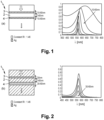
- FIG. 1 shows the spectral response of a Fabry-Pérot cavity filter 1 comprising a dielectric layer 2 with a thickness of 140 nm between two metallic reflective layers 3 and 4 of the same thickness when the two thicknesses of the reflective metallic layers 3 and 4 vary between 10 and 60 nm.
- Bandwidth adjustment can also be achieved by varying a single metal thickness, e.g., the thickness of the reflective layer 4, as shown in Figure 2 (the thickness of the reflective layer 3 remaining constant and equal to 30 nm).
- a single metal thickness e.g., the thickness of the reflective layer 4, as shown in Figure 2 (the thickness of the reflective layer 3 remaining constant and equal to 30 nm).
- the maximum transmission decreases. It therefore appears to be difficult to obtain a narrow transmission bandwidth while maintaining a higher transmission coefficient with Fabry-Pérot cavity filters.
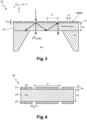
- GMR filters Guided Mode Resonance in English terminology. These filters can be implemented in the visible or infrared range. An example of such a filter can be found in the publication " Metal-dielectric structures with guided mode resonance and applications to infrared filtering and imaging" (Optics / Photonic. autoimmune Polytechnique X, 2013 - Sakat et al.). The Figure 3 illustrates the structure of a GMR filter 10 in the infrared.
- the filter 10 comprises a metal grating 11 (a "grating layer” in English terminology) comprising metal patterns spaced apart by a distance w (thus forming slots between each pattern) placed on a dielectric layer 12 which acts as a waveguide.
- the metal patterns are repeated according to a period d.
- the coupling between the waveguide mode and the resonances of the metal patterns gives a resonance wavelength.
- the wavelength depends essentially on the thickness of the dielectric layer 12.
- the filter 20 comprises a first metal network 21 comprising metal patterns arranged periodically according to a period d and spaced by a gap a, placed on a dielectric layer 22 which acts as a waveguide, itself above a second metal network 23 similar to the first network 21.
- a first metal network 21 comprising metal patterns arranged periodically according to a period d and spaced by a gap a, placed on a dielectric layer 22 which acts as a waveguide, itself above a second metal network 23 similar to the first network 21.
- the different parameters which are the thickness td of the dielectric layer, the period d, the gap a and the thickness of the metal patterns tm, will make it possible to adjust the transmission wavelength, the bandwidth and the maximum transmission.
- each 32Pi dielectric layer here has a different thickness to allow the corresponding wavelength to pass through.
- the guided mode resonance filter to work effectively, a higher repetition of the grating period is required. Furthermore, to achieve transmission of different wavelengths, a different grating period must be used for each pixel. The difficulty in mastering the technological realization of gratings can therefore lead to performance problems for pixelated image sensors. Finally, with a predefined pixel size for each pixel, the number of metal patterns is different for different pixels, again leading to implementation difficulties.
- the invention provides a solution to the problems mentioned above, by proposing a multispectral filter for electromagnetic radiation with a good compromise between the maximum transmission for each wavelength and the bandwidth, while overcoming the manufacturing problems mentioned above.
- the Fabry Pérot cavity filter is made with a conventional continuous metal reflector while the second reflector is a discontinuous metal grating of the "metal grating layer" type.
- Such an architecture offers both the adjustment flexibility of double grating filters and simplicity of manufacture since only one discontinuous layer needs to be made.
- it is perfectly possible to make a filter according to the invention making it possible to filter different colors (red, blue, green for example) with a repetition period of the patterns of the metal grating which remains constant, whatever the color, and by adjusting for example the gap between the patterns from one color to another.
- the filter according to the invention makes it possible to obtain more satisfactory performances in terms of compromise between maximum transmission and narrowness of the bandwidth (in particular compared to conventional filters in which the metal thickness is increased).
- the filter according to the invention acts as a Fabry-Pérot cavity resonator formed by the tri-layer "continuous metal layer - dielectric layer - metal network" and that the filtered wavelength is essentially determined by the thickness of the dielectric layer. The presence of at least two different thicknesses therefore ensures operation on at least two wavelengths and therefore the production of a pixelated filter, each pixel corresponding to a wavelength.
- the metal networks are preferentially located on the lower part of the filter while the continuous reflective layers are located on the upper part of the filter.
- the multispectral filter according to the invention comprises metal networks located on the upper part of the filter and continuous reflective layers located on the lower part of the filter.
- the structuring material is a resin, said structuring step being carried out by a grayscale lithography step on the layer of structuring material.
- a metal/dielectric type color filter made from a Fabry-Pérot cavity is obtained by dimensioning the thickness of the dielectric layer formed between the two metal layers. If the filtering of several colors is sought on the same component, it is then necessary to be able to obtain a dielectric thickness of variable thickness on this same component.
- This sizing is for example carried out using an electromagnetic calculation program such as the Abeles matrix transfer formalism or a diffraction calculation for pixels whose size is close to the wavelength such as the Fourier Expansion Modal Method formalism or rigorous coupled wave analysis (RCWA according to English terminology).
- an electromagnetic calculation program such as the Abeles matrix transfer formalism or a diffraction calculation for pixels whose size is close to the wavelength
- RCWA rigorous coupled wave analysis
- the index and the phase shift are known, all that remains is to determine an approximate thickness so that the cavity is centered on a particular wavelength.
- the thicknesses h of the dielectrics are then adjusted according to the desired performance (search for a good signal-to-noise ratio, maximum transmission, etc.).
- Another more empirical method consists of calculating, for several thicknesses h, the response of the stack and choosing h such that the resonance peak of the filter ( ⁇ res) is positioned in accordance with the specifications.
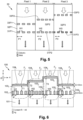
- FIG. 6 illustrates a multispectral filter 100 according to the invention.
- the multispectral filter 100 comprises a plurality of color filters Fi (i being an integer greater than or equal to 2) produced on a substrate 101 which may be, for example, a Si substrate, a Silicon On Insulator (SOI) substrate or a glass or sapphire substrate.
- a substrate 101 which may be, for example, a Si substrate, a Silicon On Insulator (SOI) substrate or a glass or sapphire substrate.
- SOI Silicon On Insulator
- 4 color filters F1 to F4 including two identical filters F1 and F4 are shown for illustration purposes only.
- the metallic patterns of the 102i networks are represented here in the form of parallelepiped blades extending along the Oz axis perpendicular to the Oxy, it being understood that these patterns can have other shapes such as cylindrical pillar shapes (square, circular, elliptical, etc.) spaced from each other by a distance Wi and repeated according to a period P.
- the period P is constant for all the metal gratings 102i.
- the repetition period P is advantageously chosen to be strictly less than the wavelengths of the color filters forming the filter according to the invention.
- the material used for the reflective metal layers 102i and 104i is preferably identical and can be, for example, Ag or Au for applications in the visible range.
- the material used for the 103i dielectric patterns can be for example SiO 2 , SiN or even a resin intended to be used in lithography.
- each space between the metal patterns of the 102i arrays is filled with the dielectric material used for the 103i dielectric patterns.
- the set of metal layers 104i can be seen as a continuous metal layer of constant thickness EC with staircase steps covering the upper surfaces of the dielectric patterns 103i as well as, optionally, the sides of the latter.
- the set of 102i metal gratings can be viewed as a planar metal grating with a constant repetition period P of metal patterns whose spacing Wi between adjacent patterns is likely to vary from one color filter to another.
- the filter 100 therefore corresponds to a state-of-the-art Fabry-Pérot type transmission filter modified in that a discontinuous metal grating with a pattern repetition period strictly less than the transmission wavelength replaces one of the continuous reflectors of the filter.
- the other reflector remains a continuous thin metal film as in a known Fabry-Pérot cavity filter.
- the grating period is the same for all the color spectral filters Fi unlike the prior art where the grating period is different for the different color filters.
- the transmission wavelength in the structure of each filter Fi can be obtained by optimizing the thickness Ti of the dielectric cavity 103i according to the methods mentioned above and to a lesser extent the gap Wi between each pattern of a metal grating 102i.
- the transmission bandwidth corresponding to a given wavelength can be controlled by adjusting the gap Wi between each pattern of a metal grating 102i and the thickness EG of the metal grating 102i.
- the thickness EG of the metallic networks 102i is preferably greater than the thickness EC of the continuous metallic reflective layers 104i.
- the thickness EG of the metal gratings 102i is preferably greater than the penetration depth of the metal, i.e. the (minimum) thickness of the metal at which the electromagnetic wave can be transmitted with minimal energy loss (the metal is more or less transparent), so that the metal grating acts as a reflector.
- the thickness EG must therefore be greater than this value (usually the penetration depth of metals is about 5 to 10 nm)
- the filter 100 makes it possible to obtain resonant filters at several wavelengths with a satisfactory maximum transmission for each wavelength and a sufficiently narrow and substantially constant bandwidth for all the wavelengths.
- the filter 100 according to the invention also optionally comprises a dielectric overlayer 105 deposited above the continuous metal layers 104i.
- the filter 100 may also comprise a plurality of photoelectric transducers (at least two) not shown (here 4 photoelectric transducers would be necessary) opposite each color filter Fi.
- the transducers may be under the substrate 101, formed inside the latter or above the latter.
- the photoelectric transducers may operate either as a collector of light coming from the filters or as an emitter of light towards the filters. If they are collectors, the transducers may be for example CMOS type photodiodes. If they are emitters, the transducers may be for example LED diodes, QLED type diodes or LASER diodes, the emitters in this case having a broader emission spectrum than that of the corresponding Fabry-Pérot cavities.
- the angle of incidence is a normal angle while a transverse magnetic polarization is used.
- Silver Ag is used here as the metal for the reflective layers and the cavity, substrate and cover material are made of SiO2 with a constant refractive index of 1.46 for illustration purposes. The choice of materials and dimensions is obviously not limited to that shown here.
- the use of a greater thickness of continuous metal layer makes it possible to narrow the transmission bandwidth compared to that of the spectrum S1 of a standard Fabry-Pérot filter: however, the increase in thickness leads to a decrease in the maximum transmission.
- the use of a thick metal network structure according to the invention makes it possible to increase the transmission coefficient while having a narrow bandwidth (- 25 nm).
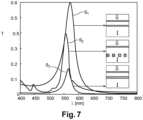
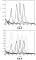
- FIG. 8 shows the spectral response of a multispectral filter such as that of the Figure 6 with the following dimensions for each Fi color filter: F1 F2 F3 F4 P (nm) 290 290 290 290 Ti (nm) 110 140 160 180 Wi (nm) 50 150 120 90 ⁇ (nm) 485 555 600 655 LMH (nm) ⁇ 25 ⁇ 25 ⁇ 25 ⁇ 25 ⁇ 25
- the thickness of the continuous reflective layer is 30 nm for each of the color filters and the thickness of the metal grating patterns for each color filter is 60 nm.
- figure 9 shows the spectral response of the figure 8 on which we superimpose (in dotted lines) the spectral response of a multispectral filter according to the state of the art with Fabry-Pérot cavities with continuous reflective layers with a thickness of 30nm.
- the filter according to the invention offers more parameters to be varied to adjust both the wavelength, the maximum transmission and the bandwidth while the state-of-the-art filter requires the wavelength to be precisely fixed as a function of the thickness of the dielectric pattern without it being possible to correct or compensate for certain manufacturing-related limitations.
- the fact of being able to vary the gap Wi makes it possible to influence the transmission and the bandwidth.
- adjusting the period makes it possible to influence the transmission and the bandwidth.
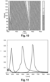
- FIG. 10 shows a transmission mapping as a function of the spacing W between the patterns of a metal grating of a color filter of a multispectral filter according to the invention, for a grating period of 290 nm and a dielectric cavity thickness of 180 nm. It can be seen that fine tuning of the wavelength can also be achieved by appropriately choosing the spacing W.
- the selection of the period P of repetition of the patterns of the metallic grating can be arbitrary provided that this period is of dimension smaller than the wavelength (in other words, the period P must be strictly smaller than the smallest wavelength to be filtered).
- the spacing Wi between the patterns can be optimized separately once the thickness Ti of the cavity is determined.
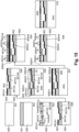
- Figure 11 shows another example of spectral response of a multispectral filter according to the invention with a period P of 260 nm and predetermined cavity thicknesses Ti to filter 3 color channels (here specifically blue, green and red).
- the spacing Wi between the patterns of each metal grating corresponding to a color was optimized separately to obtain the highest possible transmission while having a narrow bandwidth (still of the order of 25 nm) for each of the wavelengths.
- FIG. 12 shows the different stages of a method 200 for manufacturing a multispectral filter according to the invention.
- the first step 201 of the method 200 consists of starting from a substrate 300 which can for example be an Si substrate, a Silicon on Insulator SOI substrate (for “Silicon On Insulator” according to English terminology) or a glass or sapphire substrate.
- a substrate 300 which can for example be an Si substrate, a Silicon on Insulator SOI substrate (for “Silicon On Insulator” according to English terminology) or a glass or sapphire substrate.
- Step 201 is followed by a step 202 consisting of depositing a layer of resin 301 on the substrate 300.
- the method 200 then comprises a step 203 of structuring the resin layer 301 aimed at creating spaces 302i by lithography by removing material in the resin layer 301: the spaces 302i are intended to receive the metal patterns of the metal network of each color filter.
- the spaces 302i are intended to receive the metal patterns of the metal network of each color filter.
- two series of spaces 3021 and 3022 are shown, each corresponding to a color filter.
- This step thus makes it possible to fix not only the repetition period P in each metal network (corresponding to the width of the resin pattern of each series to which the width of a space in the series is added) but also the gap Wi (corresponding to the width of a pattern) between each pattern of a metal network.
- the method 200 then comprises a step 204 of depositing metal both in the spaces 302i but also above the remaining resin areas of the layer 301.
- This deposition makes it possible to form the metal patterns 303i in the spaces 302i for each of the metal networks corresponding to a color filter.
- the metal can be deposited in a conformal manner by chemical vapor deposition (CVD) or physical vapor deposition (PVD).
- the thickness of the deposited metal is, for example, around 60 nm.
- the metal deposition step is followed by a step 205 of removing the metal remaining on the resin and the remaining resin in order to retain only the metal patterns 303i.
- the method 200 according to the invention then comprises a step 206 of depositing a layer of dielectric material 304 intended to form the dielectric patterns of each of the color filters of the filter according to the invention.
- This layer 304 is optionally planarized by an etch-back type etching step and/or a CMP (Chemical Mechanical Polishing) step.
- the material of the layer 304 is preferably but not limited to a transparent material in the visible range such as an organic material of the polymer or inorganic type (oxide, silicon nitride, alumina, etc.).
- the deposition is for example a deposition carried out by a physical vapor deposition (PVD) technique or chemical vapor deposition (CVD) or low pressure chemical vapor deposition (LPCVD) or plasma enhanced chemical vapor deposition (PECVD).
- PVD physical vapor deposition
- CVD chemical vapor deposition
- LPCVD low pressure chemical vapor deposition
- PECVD plasma enhanced chemical vapor deposition
- the invention is not limited to the visible range and that other materials transparent to other wavelengths, in the infrared for example (for example using silicon), can be used.
- the dielectric material fills the spaces between the metal patterns 303i.
- the thickness of the dielectric layer 304 (if applicable after planarization) is chosen to correspond to the height of the thickest dielectric cavity (here designated by the thickness T2) for all of the color filters.
- Step 206 is followed by a step 207 of depositing a second layer of resin 305 on the dielectric layer 304.
- the resin layer 305 is structured, for example by lithography, so as to leave visible the zone P of the dielectric layer 304 corresponding to the dielectric pattern of the first color filter to be formed.
- Step 208 is followed by a step 209 during which the dielectric layer in the P zone is etched to a given thickness T1 so as to obtain the desired thickness of the dielectric pattern 3061 of the Fabry-Pérot cavity.
- This etching can be a dry or wet etching.
- Steps 207 to 209 may be repeated if more than two color filters are to be obtained.
- Step 210 then consists of removing the remaining resin 305 so as to release on the surface the dielectric pattern 3062 of Fabry-Pérot cavity of thickness T2.
- This continuous 307 planar reflective layer is conformally deposited by chemical vapor deposition (CVD) or physical vapor deposition (PVD).
- a multispectral filter is obtained which conforms to that of the Figure 6 in which the metal networks are located on the lower part of the filter while the continuous reflective layers are located on the upper part of the filter.
- This filter 400 according to a second embodiment of the invention is represented schematically in Figure 13 . Its structure is identical to that of the filter according to the first embodiment of the invention shown in Figure 6
- the only difference between the 400 filter and the 100 filter is to reverse the position of the continuous metallic reflective layers 104i and the metallic networks 102i; thus, in Figure 13 , the 102i metal networks are located on the upper part of the Fabry-Pérot cavities while they were in the lower part in the filter of the Figure 6 .
- the reference numbers of the structural elements and dimensions are common to both the 100 and 400 filters.
- FIG 14 shows the superposition of the spectral response of two color filters, one used in filter 100 of the Figure 6 (solid line) and the other used in the 400 filter of the Figure 13 (dotted line).
- the chosen dimensions are the same for both color filters with a dielectric pattern thickness T of 180 nm, a repetition period P of the metal grating patterns of 260 nm and a spacing W between the metal grating patterns of 70 nm. It can be seen that the two spectral responses overlap: it is therefore possible to use the structure of the 100 filter and the 400 filter indifferently without modifying the spectral response.
- FIG. 15 shows the different steps of a method 500 for manufacturing a multispectral filter according to the second embodiment of the invention.
- the first step 501 of the method 500 consists of starting from a substrate 600 which can for example be an Si substrate, a Silicon on Insulator SOI substrate (for “Silicon On Insulator” according to English terminology) or a glass or sapphire substrate.
- a substrate 600 which can for example be an Si substrate, a Silicon on Insulator SOI substrate (for “Silicon On Insulator” according to English terminology) or a glass or sapphire substrate.
- Step 501 is followed by a step 502 consisting of depositing a layer of resin 301 on the substrate 300.
- the resin layer 601 is then structured.
- the structuring of the resin layer 601 is carried out by a lithography step.
- This lithography may preferably be a grayscale lithography according to the English electronic or optical terminology.
- Other lithography techniques such as two-photon lithography or nano-imprinting may also be used for producing the resin structure 601.
- the structured resin layer 601 comprises a plurality of patterns 601Ai (here 4 patterns 601A1, 601A2, 601A3 and 601A4).
- Step 503 is followed by a step 504 of depositing a reflective metal layer 602, for example with a thickness of between 20 and 50 nm, covering the patterns 601Ai of the structured sub-layer 401.
- This reflective layer 602 forms the first reflective layer of the future Fabry-Pérot cavity type color filters.
- the reflective layer 602 must at least continuously cover each upper surface of the patterns 601Ai, it being understood that it could also be deposited on the sides of the patterns 601Ai.
- This reflective layer 602 is for example deposited conformally by chemical vapor deposition (CVD) or physical vapor deposition (PVD).
- CVD chemical vapor deposition
- PVD physical vapor deposition
- the next step consists of depositing a layer made of the dielectric material intended to form the dielectric patterns of the Fabry-Pérot cavities.
- the layer of dielectric material covers all of the patterns 601Ai covered with the reflective layer 602.
- the layer has an upper surface (not necessarily flat) each point of which is located at a height, relative to the substrate 600, greater than the maximum reference height Hmax.
- the material of the layer is preferably, but not limited to, a transparent material in the visible range such as an organic material of the polymer or inorganic type (oxide, silicon nitride, alumina, etc.).
- the deposit is preferably a conformal deposit, for example carried out using a physical vapor deposition technique (PVD) or chemical vapor deposition (CVD) or low pressure chemical vapor deposition (LPCVD) or plasma-enhanced chemical vapor deposition (PECVD).
- PVD physical vapor deposition technique
- CVD chemical vapor deposition
- LPCVD low pressure chemical vapor deposition
- PECVD plasma-enhanced chemical vapor deposition
- the method 500 then comprises a step 505 of planarization of the layer produced in the dielectric material intended to form the dielectric patterns of the Fabry-Pérot cavities so as to form a surface-planarized layer 603 by removal of the dielectric material from the previously deposited dielectric layer.
- planarization is carried out with a stop on the reflective layer 602 located at its highest level (i.e. at the level of the reference height of the patterns 601A1 and 601A4).
- the method 500 then comprises a step 506 of conformal deposition of a layer 604 of the same dielectric material intended to form the dielectric patterns of the Fabry-Pérot cavities.
- This step is for example carried out by a PVD, CVD, LPCVD or PECVD deposition technique.
- the height of the layer 604 is noted hc, the height being measured perpendicular to the plane of the substrate 600.
- a plurality of dielectric patterns of Fabry-Pérot cavity 605Ai are obtained (here four patterns 605A1, 605A2, 605A3 and 605A4).
- hdiel_1 and hdiel_4 are here directly equal to the height hc of layer 604.
- the height is technologically determined by the difference in height between that of the highest 601A1 resin pattern Hmax and the height of the 601Ai resin pattern to which the height of the second 604 dielectric layer is added.
- Step 507 of the method 500 then consists of depositing a second metal layer 606, with a thickness preferably greater than that of the first metal layer 602, for example of the order of 60 nm, covering the Fabry-Pérot cavity patterns 605Ai.
- This planar and continuous metal layer 602 is intended to form the upper network of metal patterns of the Fabry-Pérot cavity type color filters.
- the metal layer 606 is deposited conformally by CVD or PVD deposition.
- the method 500 then comprises a step 508 of structuring a resin layer aimed at creating spaces 607Ai by lithography by removing material in the resin layer.
- the spaces 607Ai are intended to receive the metal patterns of the metal network of each color filter. According to the invention, it is appropriate to have at least two series of spaces corresponding to at least two color filters. Here, for example purposes only, four series of spaces 607A1 to 607A4 are shown, each corresponding to a color filter. This step thus makes it possible to fix not only the repetition period P in each metal network (corresponding to the width of the resin pattern of each series to which we add the width of a space in the series) but also the gap Wi (corresponding to the width of a space in the series) between each pattern of a metal network.
- Step 509 then consists of etching the metal of the metal layer 606 not protected by the resin to create the metal patterns 308i in for each of the metal networks corresponding to a color filter.
- Step 510 optionally deposits a planarized dielectric overlayer 609 above and between the continuous metal pattern arrays.
Landscapes
- Physics & Mathematics (AREA)
- General Physics & Mathematics (AREA)
- Optics & Photonics (AREA)
- Spectroscopy & Molecular Physics (AREA)
- Optical Filters (AREA)
Applications Claiming Priority (1)
| Application Number | Priority Date | Filing Date | Title |
|---|---|---|---|
| FR2309032A FR3152606A1 (fr) | 2023-08-29 | 2023-08-29 | Filtre multispectral pour une radiation électromagnétique et procédé de fabrication dudit filtre |
Publications (2)
| Publication Number | Publication Date |
|---|---|
| EP4528337A2 true EP4528337A2 (de) | 2025-03-26 |
| EP4528337A3 EP4528337A3 (de) | 2025-07-30 |
Family
ID=89897343
Family Applications (1)
| Application Number | Title | Priority Date | Filing Date |
|---|---|---|---|
| EP24195793.5A Pending EP4528337A3 (de) | 2023-08-29 | 2024-08-22 | Multispektraler filter für elektromagnetische strahlung und verfahren zu seiner herstellung |
Country Status (3)
| Country | Link |
|---|---|
| US (1) | US20250081648A1 (de) |
| EP (1) | EP4528337A3 (de) |
| FR (1) | FR3152606A1 (de) |
Family Cites Families (3)
| Publication number | Priority date | Publication date | Assignee | Title |
|---|---|---|---|---|
| CN109613633B (zh) * | 2018-12-29 | 2021-06-01 | 江西师范大学 | 一种超窄多频带光学传感器 |
| CN110568525B (zh) * | 2019-08-08 | 2020-08-25 | 武汉大学 | 基于微纳起偏器及f-p腔结构的彩色纳米印刷器件 |
| CN113871437A (zh) * | 2021-09-18 | 2021-12-31 | 深圳大学 | 显示器件及其制备方法和显示装置 |
-
2023
- 2023-08-29 FR FR2309032A patent/FR3152606A1/fr active Pending
-
2024
- 2024-08-22 EP EP24195793.5A patent/EP4528337A3/de active Pending
- 2024-08-28 US US18/818,077 patent/US20250081648A1/en active Pending
Non-Patent Citations (2)
| Title |
|---|
| I. L. GOMES DE SOUZAV. F. RODRIGUEZ-ESQUERRED. F. RÊGO: "Filtres grand angle à base de nanorésonateurs pour le spectre visible", APPL. OPTER., vol. 57, 2018, pages 6755 - 6759 |
| SAKAT ET AL.: "Structures métal-diélectriques à résonance de mode guidé et applications au filtrage et à l'imagerie infrarouge", OPTICS / PHOTONIC. ECOLE POLYTECHNIQUE X, 2013 |
Also Published As
| Publication number | Publication date |
|---|---|
| EP4528337A3 (de) | 2025-07-30 |
| FR3152606A1 (fr) | 2025-03-07 |
| US20250081648A1 (en) | 2025-03-06 |
Similar Documents
| Publication | Publication Date | Title |
|---|---|---|
| EP2390689B1 (de) | Optischer Filter für Strahlen mit variablen Einfallwinkeln und Detektor mit einem solchen Filter | |
| EP3239671B1 (de) | Vorrichtung zur erfassung von elektromagnetischer strahlung mit einer einkapselungsstruktur, die mindestens einen interferenzfilter umfasst | |
| EP3607585B1 (de) | Vorrichtung und verfahren zur multispektralen bildgebung im infrarotbereich | |
| EP2559069B1 (de) | Optischer mono- oder mehrfrequenzfilter und detektor mit einem derartigen filter | |
| FR3020878A1 (fr) | Dispositif de filtrage optique comportant des cavites fabry-perot a couche structuree et d'epaisseurs differentes | |
| WO2010046369A1 (fr) | Structure de filtrage optique en longueur d'onde et capteur d'images associé | |
| FR2904432A1 (fr) | Structure matricielle de filtrage optique et capteur d'images associe | |
| FR3083646A1 (fr) | Capteur d'images | |
| EP0742453A1 (de) | Breitbandspiegel hohen Reflektionsgrads und Verfahren zur Herstellung eines solchen Spiegels | |
| EP3855068A1 (de) | Vorrichtung zur verteilten lichtprojektion | |
| FR2964795A1 (fr) | Photodetecteur et matrice de détection correspondante | |
| FR3083644A1 (fr) | Capteur d'images | |
| EP4009456B1 (de) | Verfahren zur herstellung eines verteilten bragg-spiegels | |
| EP4220723B1 (de) | Verfahren zur herstellung eines multispektralen filters für elektromagnetische strahlung | |
| EP4303633B1 (de) | Multispektrale filtermatrix mit gekrümmten fabry-perot-filtern und verfahren zur herstellung | |
| EP4528337A2 (de) | Multispektraler filter für elektromagnetische strahlung und verfahren zu seiner herstellung | |
| EP3814814B1 (de) | Spektralfilter mit mindestens zwei gekoppelten fabry-perot-strukturen | |
| EP2746826B1 (de) | Optischer Frequenzfilter und Detektor, der mit einem solchen Filter ausgestattet ist | |
| EP4478416A1 (de) | Verfahren zur herstellung eines multispektralen filters für elektromagnetische strahlung | |
| EP4584622A1 (de) | Spektralfilter mit gekoppelten resonatoren | |
| EP3043166B1 (de) | Optische fokalisierungsvorrichtung | |
| EP4034923B1 (de) | Optisches system und verfahren zu dessen herstellung | |
| FR3140991A1 (fr) | Filtre optique pour capteur multispectral | |
| FR3153430A1 (fr) | Procédé de fabrication d’une matrice de filtrage multispectral à filtres de Fabry-Pérot incurvés |
Legal Events
| Date | Code | Title | Description |
|---|---|---|---|
| PUAI | Public reference made under article 153(3) epc to a published international application that has entered the european phase |
Free format text: ORIGINAL CODE: 0009012 |
|
| STAA | Information on the status of an ep patent application or granted ep patent |
Free format text: STATUS: REQUEST FOR EXAMINATION WAS MADE |
|
| 17P | Request for examination filed |
Effective date: 20240822 |
|
| AK | Designated contracting states |
Kind code of ref document: A2 Designated state(s): AL AT BE BG CH CY CZ DE DK EE ES FI FR GB GR HR HU IE IS IT LI LT LU LV MC ME MK MT NL NO PL PT RO RS SE SI SK SM TR |
|
| PUAL | Search report despatched |
Free format text: ORIGINAL CODE: 0009013 |
|
| AK | Designated contracting states |
Kind code of ref document: A3 Designated state(s): AL AT BE BG CH CY CZ DE DK EE ES FI FR GB GR HR HU IE IS IT LI LT LU LV MC ME MK MT NL NO PL PT RO RS SE SI SK SM TR |
|
| RIC1 | Information provided on ipc code assigned before grant |
Ipc: G02B 1/00 20060101AFI20250626BHEP Ipc: G02B 5/20 20060101ALI20250626BHEP Ipc: G02B 5/28 20060101ALI20250626BHEP |