EP4525317A2 - Dispositif terminal et système de communication - Google Patents
Dispositif terminal et système de communication Download PDFInfo
- Publication number
- EP4525317A2 EP4525317A2 EP24201056.9A EP24201056A EP4525317A2 EP 4525317 A2 EP4525317 A2 EP 4525317A2 EP 24201056 A EP24201056 A EP 24201056A EP 4525317 A2 EP4525317 A2 EP 4525317A2
- Authority
- EP
- European Patent Office
- Prior art keywords
- switch
- antenna
- terminal device
- circuitry
- coupled
- Prior art date
- Legal status (The legal status is an assumption and is not a legal conclusion. Google has not performed a legal analysis and makes no representation as to the accuracy of the status listed.)
- Pending
Links
Images


Classifications
-
- H—ELECTRICITY
- H04—ELECTRIC COMMUNICATION TECHNIQUE
- H04L—TRANSMISSION OF DIGITAL INFORMATION, e.g. TELEGRAPHIC COMMUNICATION
- H04L27/00—Modulated-carrier systems
- H04L27/18—Phase-modulated carrier systems, i.e. using phase-shift keying
- H04L27/20—Modulator circuits; Transmitter circuits
-
- G—PHYSICS
- G06—COMPUTING OR CALCULATING; COUNTING
- G06K—GRAPHICAL DATA READING; PRESENTATION OF DATA; RECORD CARRIERS; HANDLING RECORD CARRIERS
- G06K19/00—Record carriers for use with machines and with at least a part designed to carry digital markings
- G06K19/06—Record carriers for use with machines and with at least a part designed to carry digital markings characterised by the kind of the digital marking, e.g. shape, nature, code
- G06K19/067—Record carriers with conductive marks, printed circuits or semiconductor circuit elements, e.g. credit or identity cards also with resonating or responding marks without active components
- G06K19/07—Record carriers with conductive marks, printed circuits or semiconductor circuit elements, e.g. credit or identity cards also with resonating or responding marks without active components with integrated circuit chips
- G06K19/0701—Record carriers with conductive marks, printed circuits or semiconductor circuit elements, e.g. credit or identity cards also with resonating or responding marks without active components with integrated circuit chips at least one of the integrated circuit chips comprising an arrangement for power management
- G06K19/0707—Record carriers with conductive marks, printed circuits or semiconductor circuit elements, e.g. credit or identity cards also with resonating or responding marks without active components with integrated circuit chips at least one of the integrated circuit chips comprising an arrangement for power management the arrangement being capable of collecting energy from external energy sources, e.g. thermocouples, vibration, electromagnetic radiation
- G06K19/0708—Record carriers with conductive marks, printed circuits or semiconductor circuit elements, e.g. credit or identity cards also with resonating or responding marks without active components with integrated circuit chips at least one of the integrated circuit chips comprising an arrangement for power management the arrangement being capable of collecting energy from external energy sources, e.g. thermocouples, vibration, electromagnetic radiation the source being electromagnetic or magnetic
- G06K19/0709—Record carriers with conductive marks, printed circuits or semiconductor circuit elements, e.g. credit or identity cards also with resonating or responding marks without active components with integrated circuit chips at least one of the integrated circuit chips comprising an arrangement for power management the arrangement being capable of collecting energy from external energy sources, e.g. thermocouples, vibration, electromagnetic radiation the source being electromagnetic or magnetic the source being an interrogation field
-
- G—PHYSICS
- G06—COMPUTING OR CALCULATING; COUNTING
- G06K—GRAPHICAL DATA READING; PRESENTATION OF DATA; RECORD CARRIERS; HANDLING RECORD CARRIERS
- G06K19/00—Record carriers for use with machines and with at least a part designed to carry digital markings
- G06K19/06—Record carriers for use with machines and with at least a part designed to carry digital markings characterised by the kind of the digital marking, e.g. shape, nature, code
- G06K19/067—Record carriers with conductive marks, printed circuits or semiconductor circuit elements, e.g. credit or identity cards also with resonating or responding marks without active components
- G06K19/07—Record carriers with conductive marks, printed circuits or semiconductor circuit elements, e.g. credit or identity cards also with resonating or responding marks without active components with integrated circuit chips
- G06K19/0723—Record carriers with conductive marks, printed circuits or semiconductor circuit elements, e.g. credit or identity cards also with resonating or responding marks without active components with integrated circuit chips the record carrier comprising an arrangement for non-contact communication, e.g. wireless communication circuits on transponder cards, non-contact smart cards or RFIDs
-
- H—ELECTRICITY
- H02—GENERATION; CONVERSION OR DISTRIBUTION OF ELECTRIC POWER
- H02J—CIRCUIT ARRANGEMENTS OR SYSTEMS FOR SUPPLYING OR DISTRIBUTING ELECTRIC POWER; SYSTEMS FOR STORING ELECTRIC ENERGY
- H02J50/00—Circuit arrangements or systems for wireless supply or distribution of electric power
- H02J50/001—Energy harvesting or scavenging
-
- H—ELECTRICITY
- H02—GENERATION; CONVERSION OR DISTRIBUTION OF ELECTRIC POWER
- H02J—CIRCUIT ARRANGEMENTS OR SYSTEMS FOR SUPPLYING OR DISTRIBUTING ELECTRIC POWER; SYSTEMS FOR STORING ELECTRIC ENERGY
- H02J50/00—Circuit arrangements or systems for wireless supply or distribution of electric power
- H02J50/20—Circuit arrangements or systems for wireless supply or distribution of electric power using microwaves or radio frequency waves
-
- H—ELECTRICITY
- H02—GENERATION; CONVERSION OR DISTRIBUTION OF ELECTRIC POWER
- H02J—CIRCUIT ARRANGEMENTS OR SYSTEMS FOR SUPPLYING OR DISTRIBUTING ELECTRIC POWER; SYSTEMS FOR STORING ELECTRIC ENERGY
- H02J50/00—Circuit arrangements or systems for wireless supply or distribution of electric power
- H02J50/80—Circuit arrangements or systems for wireless supply or distribution of electric power involving the exchange of data, concerning supply or distribution of electric power, between transmitting devices and receiving devices
-
- H—ELECTRICITY
- H04—ELECTRIC COMMUNICATION TECHNIQUE
- H04B—TRANSMISSION
- H04B5/00—Near-field transmission systems, e.g. inductive or capacitive transmission systems
- H04B5/40—Near-field transmission systems, e.g. inductive or capacitive transmission systems characterised by components specially adapted for near-field transmission
- H04B5/45—Transponders
-
- H—ELECTRICITY
- H04—ELECTRIC COMMUNICATION TECHNIQUE
- H04B—TRANSMISSION
- H04B5/00—Near-field transmission systems, e.g. inductive or capacitive transmission systems
- H04B5/70—Near-field transmission systems, e.g. inductive or capacitive transmission systems specially adapted for specific purposes
- H04B5/77—Near-field transmission systems, e.g. inductive or capacitive transmission systems specially adapted for specific purposes for interrogation
-
- H—ELECTRICITY
- H04—ELECTRIC COMMUNICATION TECHNIQUE
- H04B—TRANSMISSION
- H04B5/00—Near-field transmission systems, e.g. inductive or capacitive transmission systems
- H04B5/70—Near-field transmission systems, e.g. inductive or capacitive transmission systems specially adapted for specific purposes
- H04B5/79—Near-field transmission systems, e.g. inductive or capacitive transmission systems specially adapted for specific purposes for data transfer in combination with power transfer
Definitions
- Various example embodiments generally relate to the field of communications and in particular, to a terminal device and a communication system comprising at least one terminal device.
- IoT internet of things
- the third generation partnership project (3GPP) has specified narrowband (NB)-IoT/enhanced machine-type communication (eMTC) and new radio (NR) RedCap before release-18 to satisfy the requirements on low cost and low power devices for wide area IoT communication.
- NB narrowband
- eMTC enhanced machine-type communication
- NR new radio RedCap
- example embodiments of the present disclosure provide a terminal device and a communication system comprising at least one terminal device, especially an A-IoT device with a single resonance antenna for simultaneous energy harvesting and binary phase modulation with a dual frequency activation signal.
- the terminal device provided by the example embodiments of the present disclosure can support binary phase shift keying (BPSK) backscatter with low complexity, cost, and a small size.
- BPSK binary phase shift keying
- a terminal device may comprise first circuitry coupled to an antenna and configured for a BPSK modulation based on a dual frequency signal received via the antenna, wherein a first frequency part of the dual frequency signal may match the antenna resonance frequency and may be used for charging an energy storage, and a second frequency part of the dual frequency signal may be used for performing the BPSK modulation at a mismatched frequency of an antenna impedance; and second circuitry coupled to the first circuitry and configured to control a state of the first circuitry for performing the BPSK modulation.
- the terminal device may further comprise third circuitry coupled to the antenna and configured for an on-off-key (OOK) modulation based on a single frequency signal received via the antenna resonance frequency, wherein the second circuitry may be coupled to the third circuitry and configured to control a state of the third circuitry for performing the OOK modulation.
- OOK on-off-key
- the antenna impedance at the single frequency may be to be mismatched and the single frequency is reflected back.
- the antenna impedance at the single frequency may be to be matched and the single frequency signal may be to charge the energy storage.
- the first circuitry in the event that the first SPST switch is in the off-state, may act as a high impedance for the first frequency part such that the first frequency part is to charge the energy storage, and the first circuitry may act as a low impedance for the second frequency part such that the second frequency is reflected back at an open end of the first or second transmission line of the first circuit.
- the OOK modulation may be enabled for both the single frequency signal and the dual frequency signal.
- either of the OOK modulation and the BPSK modulation may be enabled for the dual frequency signal.
- the first circuitry may comprise a second SPDT switch coupled to the antenna, two transmission lines of different electrical length coupled to the second SPDT switch and to a third SPDT switch, and wherein the second SPDT switch and third SPDT switch may be coupled to the second circuitry.
- the second SPDT switch and third SPDT switch may be switched in parallel to change phases for both the first frequency part and the second frequency part.
- the first circuitry may comprise a single pole triple throw (SP3T) switch coupled to the antenna, two transmission lines of different electrical length coupled to the SP3T switch and to a fourth SPDT switch, and wherein the SP3T switch and the fourth SPDT switch may be coupled to the second circuitry.
- SP3T single pole triple throw
- the SP3T switch in the event that a single frequency signal is received via the antenna, the SP3T switch may be configured in a shorted-state, and the single frequency signal may not match the antenna and may be reflected back.
- the SP3T switch in the event that a single frequency signal is received via the antenna, the SP3T switch may be configured in a direct-state together with fourth SPDT, and the single frequency signal may match the antenna and charges the energy storage; and wherein a toggling of the SP3T switch together with the fourth SPDT may be to result in the OOK modulation and a periodically energy harvesting.
- the SP3T switch in the event that the dual frequency signal is received via the antenna, the SP3T switch may be configured in a 180-degree reflected delay-state, and the fourth SPDT switch may be configured in parallel with the SP3T switch, and the second frequency part may be reflected back using the BPSK modulation, and wherein the second frequency part may be delayed by 180 degrees in the 180-degree reflected delay-state.
- the antenna may be a single resonance antenna.
- the communication system may comprise at least one terminal device of the first aspect; and at least one network device in communication with the at least one terminal device.
- references in the present disclosure to "one embodiment,” “an embodiment,” “an example embodiment,” and the like indicate that the embodiment described may include a particular feature, structure, or characteristic, but it is not necessary that every embodiment includes the particular feature, structure, or characteristic. Moreover, such phrases are not necessarily referring to the same embodiment. Further, when a particular feature, structure, or characteristic is described in connection with an embodiment, it is submitted that it is within the knowledge of one skilled in the art to affect such feature, structure, or characteristic in connection with other embodiments whether or not explicitly described.
- first and second etc. may be used herein to describe various elements, these elements should not be limited by these terms. These terms are only used to distinguish one element from another. For example, a first element could be termed a second element, and similarly, a second element could be termed a first element, without departing from the scope of example embodiments.
- the term “and/or” includes any and all combinations of one or more of the listed terms.
- circuitry may refer to one or more or all of the following:
- circuitry also covers an implementation of merely a hardware circuit or processor (or multiple processors) or portion of a hardware circuit or processor and its (or their) accompanying software and/or firmware.
- circuitry also covers, for example and if applicable to the particular claim element, a baseband integrated circuit or processor integrated circuit for a mobile device or a similar integrated circuit in server, a cellular network device, or other computing or network device.
- the term "communication network” refers to a network following any suitable communication standards, such as long term evolution (LTE), LTE-advanced (LTE-A), wideband code division multiple access (WCDMA), high-speed packet access (HSPA), narrow band Internet of things (NB-IoT) and so on.
- LTE long term evolution
- LTE-A LTE-advanced
- WCDMA wideband code division multiple access
- HSPA high-speed packet access
- NB-IoT narrow band Internet of things
- the communications between a terminal device and a network device in the communication network may be performed according to any suitable generation communication protocols, including, but not limited to, the third generation (3G), the fourth generation (4G), 4.5G, the fifth generation (5G) communication protocols, and/or beyond.
- 3G third generation
- 4G fourth generation
- 4.5G the fifth generation
- 5G fifth generation
- the term "network device” refers to a node in a communication network via which a terminal device accesses the network and receives services therefrom.
- the network device may refer to a base station (BS) or an access point (AP), for example, a node B (NodeB or NB), an evolved NodeB (eNodeB or eNB), a NRNB (also referred to as a gNB), a remote radio unit (RRU), a radio header (RH), a remote radio head (RRH), a relay, a low power node such as a femto, a pico, and so forth, depending on the applied terminology and technology.
- BS base station
- AP access point
- NodeB or NB node B
- eNodeB or eNB evolved NodeB
- NRNB also referred to as a gNB
- RRU remote radio unit
- RH radio header
- RRH remote radio head
- relay a low power node such
- terminal device refers to any end device that may be capable of wireless communication.
- a terminal device may also be referred to as a communication device, user equipment (UE), a subscriber station (SS), a portable subscriber station, a mobile station (MS), or an access terminal (AT).
- UE user equipment
- SS subscriber station
- MS mobile station
- AT access terminal
- the terminal device may include, but not limited to, a mobile phone, a cellular phone, a smart phone, voice over IP (VoIP) phones, wireless local loop phones, a tablet, a wearable terminal device, a personal digital assistant (PDA), portable computers, desktop computer, image capture terminal devices such as digital cameras, gaming terminal devices, music storage and playback appliances, vehicle-mounted wireless terminal devices, wireless endpoints, mobile stations, laptop-embedded equipment (LEE), laptop-mounted equipment (LME), USB dongles, smart devices, wireless customer-premises equipment (CPE), an Internet of things (loT) device, a watch or other wearable, a head-mounted display (HMD), a vehicle, a drone, a medical device and applications (e.g., remote surgery), an industrial device and applications (e.g., a robot and/or other wireless devices operating in an industrial and/or an automated processing chain contexts), a consumer electronics device, a device operating on commercial, a relay node, an integrated access and backhaul (I
- an issue with existing 3GPP technologies for the target use cases is the capability of cooperating with energy harvesting considering limited device size.
- Cellular devices usually consume tens or even hundreds of milliwatts power for transceiver processing.
- the typical current consumption for receive processing is about 60mA with supply voltage higher than 3.1V, while 70mA for transmit processing at 0dBm transmit power.
- the output power provided by typical energy harvester is mostly below 1 milliwatt, considering the small size of a few square centimeters for practical devices. Since the available power is far less than the consumed power, it is impractical to power cellular devices directly by energy harvesting in most cases.
- device size will be significantly increased.
- battery with much larger size e.g., AA battery
- battery with much larger size is usually used to power cellular devices, whose size can be even larger than the module itself.
- the required capacitance of a supercapacitor is at the level of a hundred mill-farads.
- the size of such supercapacitors may be larger than an NB-IoT module.
- both rechargeable batteries and supercapacitors can be more expensive than the module itself. Even purchased in large quantities, the cost of a suitable battery or supercapacitor may nearly doubles the cost of the device.
- radio frequency identification is a technology supporting battery less tags (or devices).
- the power consumption of commercial passive RFID tags can be as low as one microwatt.
- the key techniques enabling such low power consumption are envelope detection for downlink data reception, and backscatter communication for uplink data transmission.
- the RFID is designed for short-range communications whose typical effective range is less than 10 meters. As the air interface of RFID almost remains unchanged since 2005, the too-simple transmission scheme becomes the obstacle of improving its link budget and capability of supporting scalable network.
- a passive radio is a device that harnesses energy from wireless signals sent on specific carriers and/or bandwidths and charges a simple circuitry that, once activated, it will emit or reflect a signal which encodes at least the identification (ID) of the passive radio.
- the typical system architecture around a passive radio includes an activator, the passive radio and a reader.
- the activator is a device that sends an activation signal targeted at waking up the passive radio.
- the passive radio can harness energy over a range of frequencies and listen for activation signals. Once such a signal is detected, the passive radio emits or reflects a signal which is specific to that radio ID.
- the reader is a device that listens and detects the passive radio signals. The reader may or may not be collocated with the activator.
- a Device A has no energy storage and no independent signal generation/amplification, i.e., backscattering transmission.
- the Device B has energy storage, and has no independent signal generation, i.e., backscattering transmission. Use of stored energy can include amplification for reflected signals.
- the Device C has energy storage and independent signal generation, i.e., active RF components for transmission.
- the design targets for power consumptions for Device A is less than or equal to 10 ⁇ W.
- the design targets for power consumptions for Device C is less than or equal to 1 mW.
- the design targets for power consumptions for Device B is greater than Device A and less than Device C.
- the device complexity design target for Device A is that it is comparable to ultrahigh frequency (UHF) RFID.
- the device complexity design target for Device C is that the orders-of-magnitude is lower than NB-IoT.
- the device complexity design target for Device B is between Device A and Device C.
- the Ambient IoT backscatter devices A and B are quite similar, but a device B may offer lower backscatter reflection loss compared to a device A using its stored energy reserve thus offering increased coverage range compared to device A.
- a device A has no energy storage and thus will need to charge on the activation signal to wake up and initiate ID/data modulated backscattering.
- a device B has energy storage which may be harvested up front any backscattering and as such this device type does not need to harvest energy from the activation signal while modulating the backscatter.
- the embodiments of the present disclosure provide a terminal device (such as an IoT device) that solves, among other potential problems, the problem of having to choose between either high coverage (device B) or low charging resource overhead (device A). Meanwhile, the terminal device can support BPSK backscatter with low complexity, cost, and a small size.
- FIG. 1 illustrates an example ambient IoT (A-IoT) backscatter operation for device A and B related to some example embodiments of the present disclosure.
- an activator 102 at the time point 104, transmits an activation signal 106.
- Device A has no energy storage and thus will need to charge on the activation signal to wake up and initiate ID/data modulated backscattering.
- the modulation will be OOK switching the antenna load between two states: matched state (denoted as X0) for energy absorbing charging and unmatched reflecting state.
- the length of the initial charging time is the duration 108 as shown in FIG. 1 .
- a device B has energy storage which may be harvested up front and as such this device type does not need to harvest energy from the activation signal while modulating the backscatter.
- the length of the initial charging time is the duration 110 as shown in FIG 1 .
- the pros for a device A may be that it does not require up front energy harvesting so can be accessed at any point in time when both activator and reader are within reach.
- the cons may be that it has significantly lower coverage compared to a device B, and the OOK modulation has higher error rates than modulation the BPSK modulation.
- the pros for a device B may be that it has significantly better coverage compared to a device A and detection of device B transmission has lower error rate than device A's.
- the cons may be that it requires up front energy harvesting to operate.
- the energy is from either non 3GPP controlled energy source which may be more or less reliable, or from network RF harvesting which may take additional resources.
- the present disclosure proposes an A-IoT device type A with a single resonance antenna. It can support BPSK backscatter with low complexity, cost, and a small size. In some example embodiments, it can toggle between OOK for single activation frequency and BPSK plus energy harvesting for dual activation frequency.
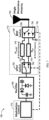
- FIG. 2 illustrates an example terminal device 200 in accordance with some example embodiments of the present disclosure.
- the terminal device 200 may be an A-IoT device type A with circuits for supporting static BPSK with a dual activation signal.
- the terminal device 200 comprises a single resonance antenna 202.
- An antenna feed of the single resonance antenna 202 is coupled to a rectifier 208 and to circuitry 214 (also referred to as first circuitry) in parallel.
- the rectifier 208 is coupled to a modulation control module 212 (also referred to as second circuitry).
- the rectifier 208 may supply the modulation control module 212 directly.
- An energy storage may be part of the rectifier 208 (such as the parallel capacitor included in the rectifier 208). It is to be understood that an energy storage may be an independent element as well. Therefore, rectifier and energy storage may be used interchangeably thereafter.
- the circuitry 214 comprises a transmission line 216 (also referred to as a first transmission line).
- the transmission line 216 is coupled to a SPST switch 220 (also referred to as a second SPST switch).
- the SPST switch 220 is coupled to a transmission line 218 (also referred to as a second transmission line).
- the circuitry 214 is configured for a BPSK modulation if a dual frequency signal is received via the single resonance antenna 202.
- the first frequency part 204 of the dual frequency signal matches the antenna resonance frequency and is used for charging an energy storage.
- the second frequency part 206 of the dual frequency signal is used for performing the BPSK modulation at a mismatched frequency of an antenna impedance.
- the circuitry 212 is configured to control a state of the circuitry 214 for performing the BPSK modulation. If the SPST switch 220 is in an off-state, the first frequency part 204 will see an open stub with an electrical length of 180° (half a wavelength), which will result in a high impedance and thus the first frequency part 204 match is unaffected. If the SPST switch 220 is in an on-state, the first frequency part 204 will see an open stub with an electrical length of 360° (one wavelength), which still will result in a high impedance and the match of the first frequency part 204 is still unaffected.
- the terminal device 200 can support BPSK backscatter with less changes to the A-IoT tag. This can ensure low complexity, low price, and small size.
- the energy storage can be constantly charged, while performing BPSK modulation at the second frequency part.
- FIG. 3 illustrates an example terminal device 300 in accordance with some example embodiments of the present disclosure.
- the terminal device 300 may be an A-IoT device type A with circuits for supporting BPSK for a dual activation signal or OOK for single frequency activation.
- the terminal device 300 may comprise a simple single resonance antenna 302.
- the simple single resonance antenna 302 may be a monopole antenna with an electrical small ground plane.
- An antenna feed of the simple single resonance antenna 302 may be coupled to a rectifier 308, to circuitry 314 and to circuitry 322 (also referred to as third circuitry) in parallel.
- the rectifier 308 may be coupled to a modulation control module 312.
- the circuitry 314 may comprise a transmission line 316.
- the transmission line 316 may be coupled to a SPST switch 320.
- the SPST switch 320 may be coupled to a transmission line 318.
- the functions of the circuitry 314 may be similar to the functions of the circuitry 214 in FIG. 2 , and thus for the purpose of simplification, it will not be described again.
- the circuitry 312 may be configured to control a state of the circuitry 322 for performing the OOK modulation.
- the antenna 202 may be matched to the first frequency part 304 of the dual activation signal.
- the circuitry 322 may comprise a SPST switch (also referred to as a first SPST switch 322). If the first SPST switch 322 is in an off-state, the circuitry 322 may be configured for performing the BPSK modulation at the second frequency part 306.
- the first frequency part 304 may constantly charge the energy storage in the rectifier 308. If the first SPST switch is in an on-state, and a single frequency signal is received via the antenna resonance frequency, the circuitry 322 may be configured for performing the OOK modulation for at the single frequency for the single frequency activation signal.
- the first stage of the terminal device 300 is with the second SPST switch 320 in an off-state (switch open) where the first frequency part 304 may see an open stub with an electrical length of 180° (half a wavelength), which will result in a high impedance and thus the first frequency part 304 match is unaffected at this first stage (as shown at m5).
- the second frequency part may see an open stub with an electrical length of 270° (3 times 90°), which is the equivalent of a short connection (as shown at m6).
- the second stage of the terminal device 300 is with the second SPST switch 320 in in an on-state (switch closed) where the first frequency part 304 may see an open stub with an electrical length of 360° (one wavelength), which still will result in a high impedance and the match of the first frequency part 304 is still unaffected at this second stage.
- the second frequency part 306 may see an open stub with an electrical length of 540° (6 times 90°), which is the equivalent of an open connection (as shown at m6).
- the resonance frequency (2133 MHz) of the antenna is unaffected by the toggling of the SPST switch 320 for BPSK modulation, which can ensure that the A-IoT tag constantly charges on the first frequency part. It is also evident that toggling the BPSK SPST switch can change the state of the mis-matched second activation frequency (3200 MHz) between an open and closed reflection, which is equivalent to a phase shift of 180°. As such, since the two shunt BPSK toggling stages are always seen as a high impedance for the first frequency part, it will have no or very low effect on the charging efficiency of the A-IoT tag.
- FIGS. 5A and 5B illustrate an example BPSK phase imbalance in accordance with some example embodiments of the present disclosure.
- FIG. 5A shows modulation factor and modulation loss due to BPSK phase imbalance.
- the OOK modulation on the single frequency can be obtained by toggling the first SPST switch 322 between off-state (where the antenna 302 is matched and energy harvesting is possible) and the on-state (where the antenna 302 is mis-matched and in reflective mode, and the energy harvesting is not possible).
- the first SPST switch 322 may have to be in off-state when applying BPSK modulation.
- the design of the terminal device 300 only has a single SPST switch in the reflecting modes for both of the modulation modes (BPSK or OOK), which can minimize the loss and increase the terminal device 300 (such as an A-IoT tag) to reader's coverage. On top of this coverage improvement there is additionally the reflection gain coming from BPSK versus OOK modulation.
- the BPSK modulation phase delta will be at 180° for a second frequency 1.5 times higher (3200 MHz) or 0.5 times lower (1066 MHz) than the first activation frequency as explained above.
- phase modulation will also occur on adjacent frequencies of those, but not with exactly 180°, as illustrated by the BPSK phase imbalance plot in FIGS. 5A and 5B for the lower frequency range (0.5 times fact at m14) and the higher frequency range (1.5 times fact at m13).
- the sensitivity of the BPSK modulation as a function of the phase imbalance is shown in Figure 5a , where it's evident that a loss of up to 3 dB will occur for phase imbalances up to 90°.
- This is equivalent to a valid/useful frequency range of approximately 2.7 GHz to 3.7 GHz for the high frequency (1.5 times fact), or an effective relative frequency range of up to 30 % for the high frequency at 3200 MHz, depending on the potential accepted modulation loss.
- the valid/useful frequency range for the low frequency range (0.5 times fact) is from 536 MHz to 1616 MHz, close to an effective relative bandwidth of 100%.
- the proposed dual activation signal A-IoT device implementation will offer reflection gains of 3dB to 6dB compared to basic single frequency activation OOK modulation within a wide range of selectable deltas between first and second frequency.
- an A-IoT device type A can enable an A-IoT device type A to support BPSK backscatter with minimal changes to the A-IoT tag. This will ensure low complexity, low price, and small size. Further, it can be possible to switch between OOK and BPSK with low added complexity.
- SOS switched open stub
- Using this switched open stub (SOS) design to change the length of a stub for an un-matched frequency to enable BPSK backscatter for an A-IoT device type A can avoid affecting the single matched resonance of the antenna used for energy harvesting. It can also allow switching between OOK and BPSK for an A-IoT tag device type A implemented with a single resonance antenna.
- FIG 6 illustrates an example terminal device 600 in accordance with some example embodiments of the present disclosure.
- BPSK or OOK modulation can be toggled for dual and single frequency activation signal(s), respectively.
- the terminal device 600 may be implemented with a combination of a SPST switch and a SPDT switch design.
- the antenna 602 may correspond to the antenna 302 in FIG. 3 .
- the circuitry 614 may correspond to the circuitry 314 in FIG. 3 .
- the rectifier 608 may correspond to the rectifier 308 in FIG. 3 .
- the modulation control module 612 may correspond to the modulation control module 312 in FIG. 3 .
- the functions of those elements may be similar to the functions of the respective elements in FIG. 3 , and thus for the purpose of simplification, it will not be described again.
- the terminal device 600 may comprise a SPDT switch 622 (also referred to as a first SPDT switch).
- the SPDT switch 622 may be coupled to the antenna 602 and the circuitry 614 in series.
- the terminal device 600 may alter between OOK and BPSK depending on the number of activation signals in frequency.
- a single frequency activation signal may cause the terminal device 600 toggle the SPDT switch 622 in the signal path to enable OOK modulation on the single transmitted activation signal (switched to 626).
- the terminal device 600 may toggle the SPST switch 620 located in between the 180° stubs for BPSK modulation for dual frequency activation signals, while configuring the SPDT switch 622 (switched to 624) to connect to the rectifier 608 for constantly charging.
- the antenna 702 may correspond to the antenna 202 in FIG. 2 .
- the circuitry 714 may correspond to the circuitry 214 in FIG. 2 .
- the rectifier 708 may correspond to the rectifier 208 in FIG. 2 .
- the modulation control module 712 may correspond to the modulation control module 212 in FIG. 2 .
- the functions of those elements may be similar to the functions of the respective elements in FIG. 2 , and thus for the purpose of simplification, it will not be described again.
- the circuitry 714 may comprise a SP3T switch 726 coupled to the antenna 702, a transmission line 716 and a transmission line 718.
- the transmission lines 716 and 718 may be of different electrical length and may be coupled to the SP3T switch 726 and to a SPDT switch 720 (also referred to as a fourth SPDT switch).
- the SP3T switch 726 and the SPDT switch 720 may be coupled to the modulation control module 712.
- a single frequency activation signal may cause the terminal device 700 toggle the SP3T switch 726 between shorted-state (bottom, 732) and direct-state (middle, 730 or top, 728) in the signal path to enable OOK modulation, while the SPDT switch 720 is conned to the direct-state (bottom, 724 or the top 772, depending on the configuration of switch 726) for the single transmitted activation signal.
- the terminal device 700 may toggle the SP3T switch 726 between 180° reflected delay-state (top, 728) and a reflected direct-state (middle, 730) in the signal path to enable BPSK modulation for a second frequency, while the SPDT switch 720 is switched in parallel for a dual frequency activation signal.
- the second frequency signal will be reflected at the rectifier and pass through the transmission line 716 twice, resulting a total relative phase shift of 180°, when switch 720 and 726 are configured for the delay-state and a relative 0° phase shift when switch 720 and 726 are configured for the direct-state.
- the first frequency will be match for both BPSK switch settings, with a different phase delay, which is unimportant as it's used for energy harvesting.
- FIG 8 illustrates an example terminal device 800 in accordance with some example embodiments of the present disclosure.
- the terminal device 800 can support static BPSK with a dual activation signal.
- the terminal device 800 may be implemented with a dual SPDT switch design.
- the antenna 802 may correspond to the antenna 202 in FIG. 2 .
- the circuitry 814 may correspond to the circuitry 214 in FIG. 2 .
- the rectifier 808 may correspond to the rectifier 208 in FIG. 2 .
- the modulation control module 812 may correspond to the modulation control module 212 in FIG. 2 .
- the functions of those elements may be similar to the functions of the respective elements in FIG. 2 , and thus for the purpose of simplification, it will not be described again.
- the circuitry 814 may comprise a SPDT switch 826 (also referred to a second SPDT switch) coupled to the antenna 802, a transmission line 816 and a transmission line 818.
- the transmission lines 816 and 818 may be of different electrical length and may be coupled to the SPDT switch 826 and to a SPDT switch 820 (also referred to a third SPDT switch).
- the SPDT switch 826 and the SPDT switch 820 may be coupled to the modulation control module 812.
- the SPDT switches 820 and 826 may be switched in parallel to change the phase for both the matched and un-matched activation frequencies.
- the SPDT switch 826 may be switched to 828 while the SPDT switch 820 is switched to 822 for a 180° reflected delay-state.
- the SPDT switch 826 may be switched to 830 while the SPDT switch 820 is switched to 824 for a reflected direct-state.
- the second frequency signal will be reflected at the rectifier and pass through the transmission line 816 twice, resulting a total relative phase shift of 180°, when switch 820 and 826 are configured for the delay-state and a relative 0° phase shift when switch 820 and 826 are configured for the direct-state.
- the first frequency will be match for both BPSK switch settings, with a different phase delay, which is unimportant as it's used for energy harvesting.
- FIG. 9 illustrates an example communication system 900 comprising the terminal device in accordance with some example embodiments of the present disclosure.
- the communication system 900 may comprise at least one terminal device 902 and at least one network device 904.
- the terminal device 902 can communicate with the network device 904. It is to be understood that this is only an example without any limitations.
- the communication system 900 may comprise any other devices, and the number of the devices are not limited.
- the communication system 900 may comprise the at least one terminal device 902 according to any embodiments discussed with FIGS. 2-3 and 6-8 .
- the terminal device may be the terminal device 200 in FIG. 2 or the terminal device 300 in FIG. 3 .
- the various embodiments of the terminal device will not be described again.
- a terminal device comprising: first circuitry coupled to an antenna and configured for a binary phase shift keying (BPSK) modulation based on a dual frequency signal received via the antenna, wherein a first frequency part of the dual frequency signal matches the antenna resonance frequency and is used for charging an energy storage of the terminal device, and a second frequency part of the dual frequency signal is used for performing the BPSK modulation at a mismatched frequency of an antenna impedance; and second circuitry coupled to the first circuitry and configured to control a state of the first circuitry for performing the BPSK modulation.
- BPSK binary phase shift keying
- Clause 2 The terminal device of clause 1, further comprising: third circuitry coupled to the antenna and configured for an on-off-key (OOK) modulation based on a single frequency signal received via the antenna resonance frequency, wherein the second circuitry is coupled to the third circuitry and configured to control a state of the third circuitry for performing the OOK modulation.
- OOK on-off-key
- Clause 3 The terminal device of clause 2, wherein the first circuitry and the third circuitry are coupled in parallel to an antenna feed.
- Clause 4 The terminal device of clause 2 or 3, wherein the third circuitry comprises a first single pole single throw (SPST) switch connected to ground.
- SPST single pole single throw
- Clause 5 The terminal device of clause 4, wherein: in the event that the single frequency signal is received via the antenna and the first SPST switch is in an on-state, the antenna impedance at the single frequency is to be mismatched and the single frequency is reflected back; in the event that the single frequency signal is received via the antenna and the first SPST switch is in an off-state, the antenna impedance at the single frequency is to be matched and the single frequency signal is to charge the energy storage; and wherein a toggling of the first SPST switch is to result in the OOK modulation and a periodically energy harvesting.
- Clause 6 The terminal device of clause 4 or 5, wherein in the event that the dual frequency signal is received via the antenna, the first SPST switch is configured in an off-state.
- Clause 7 The terminal device of any of clauses 1-6, wherein the first circuitry comprises a first transmission line coupled to the antenna, a second SPST switch coupled to the first transmission line, and a second transmission line coupled to the second SPST switch, and wherein the second SPST switch is coupled to the second and the third circuitry.
- Clause 8 The terminal device of any of clauses 4-7, wherein in the event that the first SPST switch is in the off-state, the first circuitry acts as a high impedance for the first frequency part such that the first frequency part is to charge the energy storage, and the first circuitry acts as a low impedance for the second frequency part such that the second frequency is reflected back at an open end of the first or second transmission line of the first circuit.
- Clause 9 The terminal device of clause 7 or 8, wherein a phase shift of the second frequency part varies based on an electrical length of an open stub associated with the second SPST switch in the on-state or the off-state, wherein the second SPST switch is configured to enable the BPSK modulation.
- Clause 10 The terminal device of any of clauses 1-9, wherein a phase change of the BPSK modulation is substantially 180 degrees for the second frequency part, wherein the second frequency part is substantially 1.5 times higher or substantially 0.5 times lower than the first frequency part.
- Clause 11 The terminal device of clause 2, wherein the third circuitry comprises a first single pole double throw (SPDT) switch.
- SPDT single pole double throw
- Clause 12 The terminal device of clause 11, wherein by toggling the SPDT switch: the OOK modulation is enabled for both the single frequency signal and the dual frequency signal; and either of the OOK modulation and the BPSK modulation is enabled for the dual frequency signal.
- Clause 13 The terminal device of clause 1, wherein the first circuitry comprises a second SPDT switch coupled to the antenna, two transmission lines of different electrical length coupled to the second SPDT switch and to a third SPDT switch, and wherein the second SPDT switch and third SPDT switch are coupled to the second circuitry.
- Clause 14 The terminal device of clause 11, wherein the second SPDT switch and third SPDT switch are switched in parallel to change phases for both the first frequency part and the second frequency part.
- Clause 15 The terminal device of clause 1, wherein the first circuitry comprises a single pole triple throw (SP3T) switch coupled to the antenna, two transmission lines of different electrical length coupled to the SP3T switch and to a fourth SPDT switch, and wherein the SP3T switch and the fourth SPDT switch are coupled to the second circuitry.
- SP3T single pole triple throw
- Clause 16 The terminal device of clause 15, wherein in the event that a single frequency signal is received via the antenna, the SP3T switch is configured in a shorted-state, and the single frequency signal does not match the antenna and is reflected back.
- Clause 17 The terminal device of clause 15, wherein in the event that a single frequency signal is received via the antenna, the SP3T switch is configured in a direct-state together with fourth SPDT, and the single frequency signal matches the antenna and charges the energy storage; and wherein a toggling of the SP3T switch together with the fourth SPDT is to result in the OOK modulation and a periodically energy harvesting.
- Clause 18 The terminal device of clause 18, wherein in the event that the dual frequency signal is received via the antenna, the SP3T switch is configured in a 180-degree reflected delay-state, and the fourth SPDT switch is configured in parallel with the SP3T switch, and the second frequency part is reflected back using the BPSK modulation, and wherein the second frequency part is delayed by 180 degrees in the 180-degree reflected delay-state.
- Clause 19 The terminal device of any of clauses 1-18, wherein the antenna is a single resonance antenna.
- Clause 20 A communication system comprising: at least one terminal device of any of clauses 1-19; and at least one network device in communication with the at least one terminal device.
Landscapes
- Engineering & Computer Science (AREA)
- Physics & Mathematics (AREA)
- Computer Hardware Design (AREA)
- Microelectronics & Electronic Packaging (AREA)
- Computer Networks & Wireless Communication (AREA)
- General Physics & Mathematics (AREA)
- Theoretical Computer Science (AREA)
- Electromagnetism (AREA)
- Signal Processing (AREA)
- Power Engineering (AREA)
- Near-Field Transmission Systems (AREA)
- Digital Transmission Methods That Use Modulated Carrier Waves (AREA)
- Transmitters (AREA)
Applications Claiming Priority (1)
| Application Number | Priority Date | Filing Date | Title |
|---|---|---|---|
| GBGB2314217.7A GB202314217D0 (en) | 2023-09-18 | 2023-09-18 | Terminal device and communication system |
Publications (2)
| Publication Number | Publication Date |
|---|---|
| EP4525317A2 true EP4525317A2 (fr) | 2025-03-19 |
| EP4525317A3 EP4525317A3 (fr) | 2025-04-30 |
Family
ID=88507315
Family Applications (1)
| Application Number | Title | Priority Date | Filing Date |
|---|---|---|---|
| EP24201056.9A Pending EP4525317A3 (fr) | 2023-09-18 | 2024-09-18 | Dispositif terminal et système de communication |
Country Status (3)
| Country | Link |
|---|---|
| US (1) | US20250097086A1 (fr) |
| EP (1) | EP4525317A3 (fr) |
| GB (1) | GB202314217D0 (fr) |
Family Cites Families (6)
| Publication number | Priority date | Publication date | Assignee | Title |
|---|---|---|---|---|
| US10079616B2 (en) * | 2014-12-19 | 2018-09-18 | University Of Washington | Devices and methods for backscatter communication using one or more wireless communication protocols including bluetooth low energy examples |
| EP3607429A4 (fr) * | 2017-04-06 | 2021-01-06 | The University of Washington | Transmission d'image et/ou de vidéo à l'aide de dispositifs de rétrodiffusion |
| US11722347B2 (en) * | 2021-01-14 | 2023-08-08 | University Of Washington | Backscatter devices and systems having digital architectures for OFDM backscatter |
| WO2023025374A1 (fr) * | 2021-08-24 | 2023-03-02 | Telefonaktiebolaget Lm Ericsson (Publ) | Système radio de rétrodiffusion résonant à modulation d'impulsions en position |
| WO2023049347A1 (fr) * | 2021-09-23 | 2023-03-30 | Ossia Inc. | Transfert d'énergie sans fil rétrodirectif par rétrodiffusion |
| WO2023087030A1 (fr) * | 2021-11-15 | 2023-05-19 | University Of Washington | Communication utilisant un bruit thermique modulé |
-
2023
- 2023-09-18 GB GBGB2314217.7A patent/GB202314217D0/en not_active Ceased
-
2024
- 2024-09-17 US US18/887,628 patent/US20250097086A1/en active Pending
- 2024-09-18 EP EP24201056.9A patent/EP4525317A3/fr active Pending
Also Published As
| Publication number | Publication date |
|---|---|
| EP4525317A3 (fr) | 2025-04-30 |
| US20250097086A1 (en) | 2025-03-20 |
| GB202314217D0 (en) | 2023-11-01 |
Similar Documents
| Publication | Publication Date | Title |
|---|---|---|
| US20250023589A1 (en) | Wireless communication method and device | |
| EP4380241A1 (fr) | Procédé de communication sans fil, dispositif terminal et dispositif de réseau | |
| US20240155566A1 (en) | Wireless communication method, terminal device and network device | |
| US12307314B2 (en) | Adaptive configuration of multistatic tag backscatter | |
| US20240276434A1 (en) | Wireless communication method, first device, and second device | |
| WO2024174216A1 (fr) | Commande de puissance d'émission d'onde porteuse et collecte d'énergie périodique pour dispositif de rétrodiffusion | |
| US20240178700A1 (en) | Wireless communication method and apparatus, and communication device | |
| US20250126572A1 (en) | Wireless communication method and device | |
| Sansoy et al. | Empowering wireless sensor networks with RF energy harvesting | |
| EP3216277B1 (fr) | Récupération d'énergie dans un réseau de communication sans fil | |
| CN111355509A (zh) | 一种射频发射机 | |
| EP4525317A2 (fr) | Dispositif terminal et système de communication | |
| KR102096203B1 (ko) | 무선 전력 전송 방식을 이용한 방사형 전력 공급 시스템 | |
| Sangare et al. | RF energy harvesting networks: Existing techniques and hardware technology | |
| WO2023193255A1 (fr) | Procédé et dispositif de communication sans fil | |
| EP4518168A1 (fr) | Procédé d'orthogonalisation post-transmission d'étiquette activatrice | |
| US20250056261A1 (en) | Low energy indication for internet of things devices | |
| WO2025137962A1 (fr) | Planification flexible pour communication de l'internet des objets ambiant | |
| WO2025201717A1 (fr) | Configuration de déplacement de fréquence | |
| US20250183731A1 (en) | Communication apparatus and device | |
| US20250338250A1 (en) | Method for wireless communication and communication devices | |
| EP4697811A1 (fr) | Procédé et dispositif de communication sans fil | |
| WO2025166743A1 (fr) | Dispositifs et procédés de communication | |
| GB2638187A (en) | Detecting and preventing oscillations | |
| EP4472252A2 (fr) | Procédé, appareil et programme informatique |
Legal Events
| Date | Code | Title | Description |
|---|---|---|---|
| PUAI | Public reference made under article 153(3) epc to a published international application that has entered the european phase |
Free format text: ORIGINAL CODE: 0009012 |
|
| STAA | Information on the status of an ep patent application or granted ep patent |
Free format text: STATUS: THE APPLICATION HAS BEEN PUBLISHED |
|
| AK | Designated contracting states |
Kind code of ref document: A2 Designated state(s): AL AT BE BG CH CY CZ DE DK EE ES FI FR GB GR HR HU IE IS IT LI LT LU LV MC ME MK MT NL NO PL PT RO RS SE SI SK SM TR |
|
| PUAL | Search report despatched |
Free format text: ORIGINAL CODE: 0009013 |
|
| AK | Designated contracting states |
Kind code of ref document: A3 Designated state(s): AL AT BE BG CH CY CZ DE DK EE ES FI FR GB GR HR HU IE IS IT LI LT LU LV MC ME MK MT NL NO PL PT RO RS SE SI SK SM TR |
|
| RIC1 | Information provided on ipc code assigned before grant |
Ipc: H04B 5/79 20240101ALI20250324BHEP Ipc: H04B 5/45 20240101ALI20250324BHEP Ipc: H02J 50/80 20160101ALI20250324BHEP Ipc: H02J 50/20 20160101ALI20250324BHEP Ipc: G06K 19/07 20060101ALI20250324BHEP Ipc: G06K 7/10 20060101ALI20250324BHEP Ipc: H04B 5/77 20240101ALI20250324BHEP Ipc: H04B 5/40 20240101AFI20250324BHEP |
|
| STAA | Information on the status of an ep patent application or granted ep patent |
Free format text: STATUS: REQUEST FOR EXAMINATION WAS MADE |
|
| 17P | Request for examination filed |
Effective date: 20251030 |