EP4525307A1 - Power transistors with resonant clamping circuits - Google Patents
Power transistors with resonant clamping circuits Download PDFInfo
- Publication number
- EP4525307A1 EP4525307A1 EP24150434.9A EP24150434A EP4525307A1 EP 4525307 A1 EP4525307 A1 EP 4525307A1 EP 24150434 A EP24150434 A EP 24150434A EP 4525307 A1 EP4525307 A1 EP 4525307A1
- Authority
- EP
- European Patent Office
- Prior art keywords
- circuit
- mosfet
- diode
- clamping
- coupled
- Prior art date
- Legal status (The legal status is an assumption and is not a legal conclusion. Google has not performed a legal analysis and makes no representation as to the accuracy of the status listed.)
- Pending
Links
Images



Classifications
-
- H—ELECTRICITY
- H02—GENERATION; CONVERSION OR DISTRIBUTION OF ELECTRIC POWER
- H02M—APPARATUS FOR CONVERSION BETWEEN AC AND AC, BETWEEN AC AND DC, OR BETWEEN DC AND DC, AND FOR USE WITH MAINS OR SIMILAR POWER SUPPLY SYSTEMS; CONVERSION OF DC OR AC INPUT POWER INTO SURGE OUTPUT POWER; CONTROL OR REGULATION THEREOF
- H02M3/00—Conversion of DC power input into DC power output
- H02M3/02—Conversion of DC power input into DC power output without intermediate conversion into AC
- H02M3/04—Conversion of DC power input into DC power output without intermediate conversion into AC by static converters
- H02M3/10—Conversion of DC power input into DC power output without intermediate conversion into AC by static converters using discharge tubes with control electrode or semiconductor devices with control electrode
- H02M3/145—Conversion of DC power input into DC power output without intermediate conversion into AC by static converters using discharge tubes with control electrode or semiconductor devices with control electrode using devices of a triode or transistor type requiring continuous application of a control signal
- H02M3/155—Conversion of DC power input into DC power output without intermediate conversion into AC by static converters using discharge tubes with control electrode or semiconductor devices with control electrode using devices of a triode or transistor type requiring continuous application of a control signal using semiconductor devices only
- H02M3/156—Conversion of DC power input into DC power output without intermediate conversion into AC by static converters using discharge tubes with control electrode or semiconductor devices with control electrode using devices of a triode or transistor type requiring continuous application of a control signal using semiconductor devices only with automatic control of output voltage or current, e.g. switching regulators
- H02M3/158—Conversion of DC power input into DC power output without intermediate conversion into AC by static converters using discharge tubes with control electrode or semiconductor devices with control electrode using devices of a triode or transistor type requiring continuous application of a control signal using semiconductor devices only with automatic control of output voltage or current, e.g. switching regulators including plural semiconductor devices as final control devices for a single load
-
- H—ELECTRICITY
- H03—ELECTRONIC CIRCUITRY
- H03K—PULSE TECHNIQUE
- H03K17/00—Electronic switching or gating, i.e. not by contact-making and –breaking
- H03K17/16—Modifications for eliminating interference voltages or currents
- H03K17/161—Modifications for eliminating interference voltages or currents in field-effect transistor switches
-
- H—ELECTRICITY
- H03—ELECTRONIC CIRCUITRY
- H03K—PULSE TECHNIQUE
- H03K17/00—Electronic switching or gating, i.e. not by contact-making and –breaking
- H03K17/08—Modifications for protecting switching circuit against overcurrent or overvoltage
- H03K17/081—Modifications for protecting switching circuit against overcurrent or overvoltage without feedback from the output circuit to the control circuit
- H03K17/0814—Modifications for protecting switching circuit against overcurrent or overvoltage without feedback from the output circuit to the control circuit by measures taken in the output circuit
- H03K17/08142—Modifications for protecting switching circuit against overcurrent or overvoltage without feedback from the output circuit to the control circuit by measures taken in the output circuit in field-effect transistor switches
-
- H—ELECTRICITY
- H02—GENERATION; CONVERSION OR DISTRIBUTION OF ELECTRIC POWER
- H02M—APPARATUS FOR CONVERSION BETWEEN AC AND AC, BETWEEN AC AND DC, OR BETWEEN DC AND DC, AND FOR USE WITH MAINS OR SIMILAR POWER SUPPLY SYSTEMS; CONVERSION OF DC OR AC INPUT POWER INTO SURGE OUTPUT POWER; CONTROL OR REGULATION THEREOF
- H02M1/00—Details of apparatus for conversion
- H02M1/08—Circuits specially adapted for the generation of control voltages for semiconductor devices incorporated in static converters
-
- H—ELECTRICITY
- H02—GENERATION; CONVERSION OR DISTRIBUTION OF ELECTRIC POWER
- H02M—APPARATUS FOR CONVERSION BETWEEN AC AND AC, BETWEEN AC AND DC, OR BETWEEN DC AND DC, AND FOR USE WITH MAINS OR SIMILAR POWER SUPPLY SYSTEMS; CONVERSION OF DC OR AC INPUT POWER INTO SURGE OUTPUT POWER; CONTROL OR REGULATION THEREOF
- H02M1/00—Details of apparatus for conversion
- H02M1/32—Means for protecting converters other than automatic disconnection
- H02M1/34—Snubber circuits
- H02M1/346—Passive non-dissipative snubbers
-
- H—ELECTRICITY
- H02—GENERATION; CONVERSION OR DISTRIBUTION OF ELECTRIC POWER
- H02M—APPARATUS FOR CONVERSION BETWEEN AC AND AC, BETWEEN AC AND DC, OR BETWEEN DC AND DC, AND FOR USE WITH MAINS OR SIMILAR POWER SUPPLY SYSTEMS; CONVERSION OF DC OR AC INPUT POWER INTO SURGE OUTPUT POWER; CONTROL OR REGULATION THEREOF
- H02M1/00—Details of apparatus for conversion
- H02M1/32—Means for protecting converters other than automatic disconnection
- H02M1/34—Snubber circuits
- H02M1/348—Passive dissipative snubbers
-
- H—ELECTRICITY
- H02—GENERATION; CONVERSION OR DISTRIBUTION OF ELECTRIC POWER
- H02M—APPARATUS FOR CONVERSION BETWEEN AC AND AC, BETWEEN AC AND DC, OR BETWEEN DC AND DC, AND FOR USE WITH MAINS OR SIMILAR POWER SUPPLY SYSTEMS; CONVERSION OF DC OR AC INPUT POWER INTO SURGE OUTPUT POWER; CONTROL OR REGULATION THEREOF
- H02M3/00—Conversion of DC power input into DC power output
- H02M3/01—Resonant DC/DC converters
-
- H—ELECTRICITY
- H03—ELECTRONIC CIRCUITRY
- H03K—PULSE TECHNIQUE
- H03K17/00—Electronic switching or gating, i.e. not by contact-making and –breaking
- H03K17/16—Modifications for eliminating interference voltages or currents
- H03K17/161—Modifications for eliminating interference voltages or currents in field-effect transistor switches
- H03K17/162—Modifications for eliminating interference voltages or currents in field-effect transistor switches without feedback from the output circuit to the control circuit
-
- H—ELECTRICITY
- H03—ELECTRONIC CIRCUITRY
- H03K—PULSE TECHNIQUE
- H03K17/00—Electronic switching or gating, i.e. not by contact-making and –breaking
- H03K17/51—Electronic switching or gating, i.e. not by contact-making and –breaking characterised by the components used
- H03K17/56—Electronic switching or gating, i.e. not by contact-making and –breaking characterised by the components used by the use, as active elements, of semiconductor devices
- H03K17/687—Electronic switching or gating, i.e. not by contact-making and –breaking characterised by the components used by the use, as active elements, of semiconductor devices the devices being field-effect transistors
-
- H—ELECTRICITY
- H03—ELECTRONIC CIRCUITRY
- H03K—PULSE TECHNIQUE
- H03K17/00—Electronic switching or gating, i.e. not by contact-making and –breaking
- H03K17/51—Electronic switching or gating, i.e. not by contact-making and –breaking characterised by the components used
- H03K17/56—Electronic switching or gating, i.e. not by contact-making and –breaking characterised by the components used by the use, as active elements, of semiconductor devices
- H03K17/687—Electronic switching or gating, i.e. not by contact-making and –breaking characterised by the components used by the use, as active elements, of semiconductor devices the devices being field-effect transistors
- H03K17/6871—Electronic switching or gating, i.e. not by contact-making and –breaking characterised by the components used by the use, as active elements, of semiconductor devices the devices being field-effect transistors the output circuit comprising more than one controlled field-effect transistor
-
- H—ELECTRICITY
- H10—SEMICONDUCTOR DEVICES; ELECTRIC SOLID-STATE DEVICES NOT OTHERWISE PROVIDED FOR
- H10D—INORGANIC ELECTRIC SEMICONDUCTOR DEVICES
- H10D84/00—Integrated devices formed in or on semiconductor substrates that comprise only semiconducting layers, e.g. on Si wafers or on GaAs-on-Si wafers
- H10D84/80—Integrated devices formed in or on semiconductor substrates that comprise only semiconducting layers, e.g. on Si wafers or on GaAs-on-Si wafers characterised by the integration of at least one component covered by groups H10D12/00 or H10D30/00, e.g. integration of IGFETs
- H10D84/811—Combinations of field-effect devices and one or more diodes, capacitors or resistors
-
- H—ELECTRICITY
- H03—ELECTRONIC CIRCUITRY
- H03K—PULSE TECHNIQUE
- H03K2217/00—Indexing scheme related to electronic switching or gating, i.e. not by contact-making or -breaking covered by H03K17/00
- H03K2217/0063—High side switches, i.e. the higher potential [DC] or life wire [AC] being directly connected to the switch and not via the load
-
- H—ELECTRICITY
- H03—ELECTRONIC CIRCUITRY
- H03K—PULSE TECHNIQUE
- H03K2217/00—Indexing scheme related to electronic switching or gating, i.e. not by contact-making or -breaking covered by H03K17/00
- H03K2217/0072—Low side switches, i.e. the lower potential [DC] or neutral wire [AC] being directly connected to the switch and not via the load
-
- H—ELECTRICITY
- H10—SEMICONDUCTOR DEVICES; ELECTRIC SOLID-STATE DEVICES NOT OTHERWISE PROVIDED FOR
- H10D—INORGANIC ELECTRIC SEMICONDUCTOR DEVICES
- H10D64/00—Electrodes of devices having potential barriers
- H10D64/20—Electrodes characterised by their shapes, relative sizes or dispositions
- H10D64/23—Electrodes carrying the current to be rectified, amplified, oscillated or switched, e.g. sources, drains, anodes or cathodes
-
- H—ELECTRICITY
- H10—SEMICONDUCTOR DEVICES; ELECTRIC SOLID-STATE DEVICES NOT OTHERWISE PROVIDED FOR
- H10D—INORGANIC ELECTRIC SEMICONDUCTOR DEVICES
- H10D8/00—Diodes
-
- H—ELECTRICITY
- H10—SEMICONDUCTOR DEVICES; ELECTRIC SOLID-STATE DEVICES NOT OTHERWISE PROVIDED FOR
- H10W—GENERIC PACKAGES, INTERCONNECTIONS, CONNECTORS OR OTHER CONSTRUCTIONAL DETAILS OF DEVICES COVERED BY CLASS H10
- H10W90/00—Package configurations
-
- H—ELECTRICITY
- H10—SEMICONDUCTOR DEVICES; ELECTRIC SOLID-STATE DEVICES NOT OTHERWISE PROVIDED FOR
- H10W—GENERIC PACKAGES, INTERCONNECTIONS, CONNECTORS OR OTHER CONSTRUCTIONAL DETAILS OF DEVICES COVERED BY CLASS H10
- H10W90/00—Package configurations
- H10W90/701—Package configurations characterised by the relative positions of pads or connectors relative to package parts
- H10W90/751—Package configurations characterised by the relative positions of pads or connectors relative to package parts of bond wires
- H10W90/756—Package configurations characterised by the relative positions of pads or connectors relative to package parts of bond wires between a chip and a stacked lead frame, conducting package substrate or heat sink
Definitions
- This description relates to semiconductor devices and, more particularly, to transistor circuits, such as field effect transistors implemented with a resonant clamping circuit, which can be used, e.g., in power converter circuits.
- Power transistors are used in a number of applications, such as consumer electronics, automotive electronics, industrial electronics, etc.
- power transistors are used in power conversion circuits, such as direct-current to direct-current (DC-DC) power converters (e.g., synchronous buck converters, etc.), where a power output of the power converter is coupled to a switch node between a high-side (HS) transistor and a low-side (LS) transistor of half-bridge circuit included in a power converter. Voltage and current overshoot and/or ringing can occur, e.g., during switching of the half-bridge circuit.
- DC-DC direct-current to direct-current
- HS high-side
- LS low-side
- Voltage and current overshoot and/or ringing can occur, e.g., during switching of the half-bridge circuit.
- Such overshoot and/or ringing can cause a voltage on a power supply node and/or the switch node to exceed a respective breakdown voltage of the HS or LS transistor, such as a drain-to-source breakdown voltage (BV dss ) of a vertical, trench-gate, power metal-oxide semiconductor field-effect transistor (MOSFET), e.g., breakdown voltage of a body diode of the MOSFET.
- BV dss drain-to-source breakdown voltage
- MOSFET metal-oxide semiconductor field-effect transistor
- One approach used to prevent such power efficiency loss and/or potential transistor damage is to increase BV dss of the transistors.
- increasing BV dss also increases on-state resistance of the transistors, such as drain-to-source on-state resistance (R dson ), which results in higher resistive losses, and also decreases power conversion efficiency.
- a circuit in a general aspect, includes a metal-oxide semiconductor field-effect transistor (MOSFET) having a gate, a source, and a drain.
- MOSFET metal-oxide semiconductor field-effect transistor
- the MOSFET has a first breakdown voltage.
- the circuit also includes a clamping circuit coupled between the drain and the source.
- the clamping circuit including a diode having a second breakdown voltage that is less than the first breakdown voltage.
- a cathode of the diode is coupled with the drain of the MOSFET.
- the clamping circuit further includes an inductor having a first terminal coupled with an anode of the diode, and a second terminal coupled with the source of the MOSFET.
- a half-bridge circuit in another general aspect, includes a high-side transistor circuit and a low-side transistor circuit.
- the high-side transistor circuit includes a first metal-oxide semiconductor field-effect transistor (MOSFET) having a gate, a source, and a drain.
- the first MOSFET has a first breakdown voltage.
- the high-side transistor circuit also includes a first clamping circuit including a first diode having a second breakdown voltage that is less than the first breakdown voltage. A cathode of the first diode is coupled with the drain of the first MOSFET.
- the first clamping circuit further includes a first inductor having a first terminal coupled with an anode of the first diode, and a second terminal coupled with the source of the first MOSFET.
- the low-side transistor circuit includes a second MOSFET including a gate, a source, and a drain.
- the second MOSFET has a third breakdown voltage.
- the drain of the second MOSFET is coupled with the source of the first MOSFET.
- the low-side transistor circuit also includes a second clamping circuit including a second diode having a fourth breakdown voltage that is less than the third breakdown voltage.
- a cathode of the second diode is coupled with the drain of the second MOSFET.
- the second clamping circuit further includes a second inductor having a first terminal coupled with an anode of the first diode, and a second terminal coupled with the source of the second MOSFET.
- a power converter circuit in another general aspect, includes an output impedance circuit, and a half-bridge circuit coupled with the output impedance circuit.
- the half-bridge circuit includes a high-side transistor circuit and a low-side transistor circuit.
- the high-side transistor circuit includes a first metal-oxide semiconductor field-effect transistor (MOSFET) having a gate, a source, and a drain.
- the first MOSFET has a first breakdown voltage.
- the high-side transistor circuit also includes a first clamping circuit including a first diode having a second breakdown voltage that is less than the first breakdown voltage. A cathode of the first diode is coupled with the drain of the first MOSFET.
- MOSFET metal-oxide semiconductor field-effect transistor
- the first clamping circuit further includes a first inductor having a first terminal coupled with an anode of the first diode, and a second terminal coupled with the source of the first MOSFET.
- the low-side transistor circuit includes a second MOSFET including a gate, a source, and a drain.
- the second MOSFET has a third breakdown voltage.
- the drain of the second MOSFET is coupled with the source of the first MOSFET.
- the low-side transistor circuit also includes a second clamping circuit including a second diode having a fourth breakdown voltage that is less than the third breakdown voltage.
- a cathode of the second diode is coupled with the drain of the second MOSFET.
- the second clamping circuit further includes a second inductor having a first terminal coupled with an anode of the first diode, and a second terminal coupled with the source of the second MOSFET.
- approaches for reducing voltage and current ringing and/or overshoot in transistors included in power converter circuits include use of clamping diodes.
- respective clamping diodes are coupled in parallel with each of a high-side (HS) transistor and a low-side (LS) transistor of a half-bridge circuit included in the power converter circuit.
- Each clamping diode can be a diode with a breakdown voltage that is less than a breakdown voltage of an associated transistor.
- such a clamping diode can be configured to enter avalanche breakdown at voltage (BV ka ) that is lower than a voltage at which an associated transistor enters avalanche breakdown (BV dss ).
- BV ka drift can further impact efficiency of the associated power converter, as well as long term reliability of the associated transistor or transistors, e.g., LS and/or HS trench-gate, vertical power metal-oxide-semiconductor field-effect transistors (MOSFETs), as well as associated circuitry of the power converter, such as drivers, controllers, etc.
- MOSFETs vertical power metal-oxide-semiconductor field-effect transistors
- This disclosure is directed to implementations that address at least some of the concerns noted above (e.g., loss of efficiency, BV ka drift, long term reliability issues).
- the implementations described herein provide for affecting discontinuous avalanche in clamping diodes, such as clamping diodes included in HS transistor circuits and/or LS transistor circuits, such the example implementations described herein.
- This discontinuous avalanche is achieved by inducing resonance in a corresponding clamping diode voltage (V ka ) and corresponding clamping diode current (I ka ), e.g., during avalanche of the clamping diode.
- this resonance is induced (affected, produced, etc.) using at least one inductance (e.g., an inductor, an aggregate of a plurality of distributed inductances, etc.) that is coupled in series with the clamping diode, and in parallel with the corresponding transistor.
- a clamping circuit for a HS transistor or a LS transistor can include a clamping diode in series with at least one clamping inductance, where the series coupled diode and inductance are coupled in parallel with an associated transistor (e.g., between a source terminal and a drain terminal of the transistor).
- FIG. 1 is a block diagram illustrating an example transistor circuit 110 with a resonant clamping circuit.
- the transistor circuit 110 includes a power MOSFET 120 and a resonant clamping circuit 130.
- the power MOSFET 120 can be a vertical, trench-gate MOSFET, such as an n-channel, power MOSFET.
- the transistor circuit 110 can be included in a power converter.
- respective implementations of the transistor circuit 110 can be included in a power converter as a HS transistor circuit of a corresponding half-bridge circuit, and a LS transistor circuit of the corresponding half-bridge circuit.
- the resonant clamping circuit 130 can include a series coupled diode and inductance (an LD circuit), where the LD circuit is coupled in parallel with the power MOSFET 120, e.g., between a source terminal and a drain terminal of the power MOSFET 120.
- Example implementations of the transistor circuit 110 are illustrated and described below with respect to, at least, FIGs. 3 , 10A-10B , 11A-11B , 12A-12B , 13A-13B and 14A-14B .
- the power MOSFET 120 and the resonant clamping circuit 130 can be implemented in a single semiconductor die.
- the transistor circuit 110 can be implemented in a first semiconductor die, while at least a clamping diode of the resonant clamping circuit 130 can be implemented in a second die.
- inductance of the resonant clamping circuit 130 can include, at least, inductance associated with electrical interconnects between the first semiconductor die and the second semiconductor die.
- the first semiconductor die and the second semiconductor die can be co-packaged (as multi-chip module in a single package assembly).
- Interconnects, such as conductive clips, wire bonds, etc., between the first semiconductor die and the second semiconductor die can be configured to provide, at least in part, an inductance of an associated resonant clamping circuit.
- FIG. 2 is a block diagram illustrating an example power converter circuit 200 that includes a half-bridge circuit 215.
- the half-bridge circuit 215 can be implemented using the transistor circuit 110 of FIG. 1 . That is, the half-bridge circuit 215 of the power converter circuit 200 can include respective implementations of the transistor circuit 110 for a HS transistor and a LS transistor of the half-bridge circuit 215.
- each of a LS transistor circuit and a HS transistor circuit of the half-bridge circuit 215 can include a corresponding resonant clamping circuit, such as those described herein.
- the half-bridge circuit 215 can be implemented using one or more of the example transistor circuits described and illustrated herein, such as the examples of, at least, FIGs. 3 , 10A-10B, 11A-11B , 12A-12B, 13A-13B and 14A-14B .
- the power converter circuit 200 also includes an output impedance circuit 240, which can be an inductive-capacitive circuit (LC circuit) for achieving power conversion, e.g., DC-DC conversion, based on a signal generated (provided, produced, etc.) on a switching node of the half-bridge circuit 215.
- the signal provided on the switching node can be an alternating current signal produced by the half-bridge circuit 215 from an input DC voltage signal.
- the power converter circuit 200 can be a synchronous buck converter, though, in some implementations, the power converter circuit 200 can implement other types of power converters, such as boost converters.
- FIG. 3 is a schematic diagram illustrating an example power converter circuit 300, which can be an implementation of the power converter circuit 200 of FIG. 2 .
- the power converter circuit 300 includes an input capacitance 305, an inductor 307, a HS transistor circuit 310hs, a LS transistor circuit 3101s, a switching node 317 (disposed between the HS transistor circuit 310hs and the LS transistor circuit 3101s), and an output impedance circuit 340.
- the input capacitance 305 can include capacitance of the HS transistor circuit 310hs and the LS transistor circuit 310ls, as well as capacitance of a main power loop of the power converter circuit 300.
- the inductor 307 can include a stray inductance of the main power loop of the power converter circuit 300.
- the HS transistor circuit 310hs includes a transistor 320hs (with a corresponding body diode shown) and a resonant clamping circuit 330hs
- the LS transistor circuit 310ls includes a transistor 320ls (with a corresponding body diode shown) and a resonant clamping circuit 330ls.
- the transistor 320hs and the transistor 320ls can be respective vertical, trench-gate MOSFETs.
- the resonant clamping circuit 330hs and the resonant clamping circuit 330ls can be respective LD circuits (e.g., series coupled diode and inductance).
- the output impedance circuit 340 includes an inductor 342 and a capacitor 344, which are configured to provide a desired DC-DC power conversion ratio, e.g., step down of an input DC voltage to a desired output DC voltage.
- FIG. 4 is a graph 400 comparing operation of an implementation of the transistor circuit of FIG. 1 , such as the HS transistor circuit 310hs of FIG. 3 , with a comparable transistor circuit with a non-resonant clamping circuit (e.g., clamping diode only), when implemented as a HS transistor circuit in a power converter circuit (e.g., the power converter circuit 300).
- time is indicated on the x-axis (increasing left to right), while drain-to-source voltage V ds of the HS transistor is indicated on the y-axis (increasing bottom to top).
- the values in the graph 400 are normalized, and the specific values of time and V ds will depend on the particular implementation.
- the dashed line 435 indicates a BV ka of respective clamping diodes of the example transistor circuits illustrated in the graph 400.
- the trace 450 illustrates V ds for a transistor circuit with a non-resonant clamping circuit
- the trace 460 illustrates V ds for a transistor circuit with a resonant clamping circuit, e.g., the HS transistor circuit 310hs of the power converter circuit 300 with a fixed clamping inductance.
- a value of the clamping inductance in this example will depend on the particular implementation.
- a clamping inductance of a HS transistor circuit such as the HS transistor circuit 310hs, can be in a range of 0.01 nanohenries (nH) to 1 nH.
- This reduction in the amount of time of periodic avalanche for the transistor circuit associated with the trace 460 can improve power conversion efficiency (e.g., a ratio of output power to input power), as well as reduce detrimental effects, such as BV ka shift, avalanche occurring in the HS transistor, etc.
- the clamping inductance values in the graph 600 are normalized, and the specific values of clamping inductance will depend on the particular implementation.
- the x-axis scale in the graph 600 is normalized to be consistent with the x-axis scale of FIG. 5 .
- increasing clamping inductance for the HS transistor circuit in this example provides small increases in ⁇ Efficiency (versus use of a non-resonant clamping circuit) while increasing peak V ds . Accordingly, any efficiency benefit associated with an increased HS clamping inductance may be outweighed by a corresponding increase in peak V ds .
- FIG. 7 is a graph comparing operation of an implementation of the transistor circuit of FIG. 1 , such as the LS transistor circuit 310ls of FIG. 3 , with a comparable transistor circuit with a non-resonant clamping circuit (e.g., clamping diode only), when implemented as a LS transistor circuit in a power converter circuit (e.g., the power converter circuit 300).
- time is indicated on the x-axis (increasing left to right), while V ds of the LS transistor is indicated on the y-axis (increasing bottom to top).
- the values in the graph of FIG. 7 are normalized, and the specific values of time and V ds will depend on the particular implementation.
- the dashed line 735 indicates a BV ka of respective clamping diodes of the example transistor circuits illustrated.
- the trace 750 illustrates V ds for a transistor circuit with a non-resonant clamping circuit
- the trace 760 illustrates V ds for a transistor circuit with a resonant clamping circuit, e.g., the LS transistor circuit 310ls of the power converter circuit 300 with a fixed clamping inductance.
- a value of the clamping inductance in this example will depend on the particular implementation.
- a clamping inductance of a LS transistor circuit can be in a range of 0.01 nanohenries (nH) to 1 nH. That is, in some implementations, such as those described herein, a clamping inductance that is implemented for a LS transistor circuit can be larger (e.g., 4-5 time larger) than a clamping inductance implemented for a corresponding HS transistor circuit. This difference can be due, at least in part, to HS transistors and LS side transistors being sized differently in a power conversion circuit. e.g., a larger transistor (e.g., higher current capacity with associated higher capacitance) being used for a LS transistor circuit than a relatively smaller transistor that is used for implementing a corresponding HS transistor circuit.
- a larger transistor e.g., higher current capacity with associated higher capacitance
- FIG. 9 is a graph illustrating power-conversion efficiency (percentage conversion efficiency) versus LS clamping inductance for a power conversion circuit including an implementation of the transistor circuit of FIG. 1 , e.g., as a LS transistor circuit.
- power-conversion efficiency in percentage
- FIG. 9 shows that power-conversion efficiency (in percentage) does not significantly change as a LS clamping inductance is increased.
- an approximately 0.2% variation was observed over the illustrated range, which covers more than three orders of magnitude of variation in LS clamping inductance. Accordingly, the benefit of reduced peak Vds associated with an increased LS clamping inductance does not cause a significant change (e.g., decrease) in associated power conversion efficiency.
- resonance period should also be considered with selecting clamping inductance values for resonant clamping circuits. For instance, clamping inductance values should be selected such that a period of resonance (T RES ) of an associated clamping circuit is less than an avalanche time T AVALANCHE for a corresponding clamping diode.
- avalanche time for the LS transistor circuit 310ls can be given (approximately) by: T AVALANCHE_LS ⁇ ⁇ L STRAY ⁇ C OSS_LS where L STRAY is an inductance value of the inductor 307 and C OSS_LS is the output capacitance of the transistor 320ls.
- L STRAY is the inductance value of the inductor 307
- I LOAD is an output current of the power converter circuit 300
- ⁇ is a factor indicating a percentage of I LOAD that is avalanche current
- BV KA is the breakdown (avalanche) voltage of the HS clamping diode
- V IN is the input voltage of the power converter circuit 300 (e.g., the voltage being converted).
- different values of clamping inductance may be used, e.g., based on the foregoing provided equations.
- Example implementations of various transistor circuits with resonant clamping circuits are respectively illustrated in FIGs. 10A-10B, 11A-11B , 12A-12B, 13A-13B and 14A-14B .
- Each of these respective implementations is illustrated as a circuit schematic ( FIGs. 10A, 11A , 12A, 13A and 14A ), and as a hybrid diagram including circuit schematic elements in combination with cross-sectional semiconductor device views ( FIGs. 10B, 11B , 12B, 13B and 14B ).
- Each of the illustrated example transistor circuits includes a MOSFET, a clamping diode and at least one clamping inductance.
- clamping inductances can include inductance from different metal structures, such as contacts, electrical interconnects, and/or other structures, such as metal spirals formed in a semiconductor device.
- resistors can be implemented using polysilicon structures, diffusion structures, metal structures, etc.
- capacitors can be implemented using polysilicon electrodes disposed in dielectric lined trenches that are formed in highly doped semiconductor regions, or can be implemented with a dielectric (e.g., oxide) disposed between two conductive plates (e.g., metal plate and/or doped polysilicon plates).
- dielectric e.g., oxide
- conductive plates e.g., metal plate and/or doped polysilicon plates.
- FIGs. 10B, 11B , 12B, 13B and 14B same semiconductor device structures (clamping diode and trench-gate MOSFET structures) are illustrated in the hybrid diagrams of FIGs. 10B, 11B , 12B, 13B and 14B . In some implementations, structures other than those illustrated could be used. Further, certain aspects of the MOSFET (e.g., gate, source and drain terminals) and the clamping diode (anode and cathode) of the example transistor circuits are referenced in, and discussed with respect to FIGs. 10A and 10B . However, for purposes of brevity and clarity, these elements may not be specifically referenced and/or described with respect to the other example transistor circuit implementations of FIGs. 11A-11B , 12A-12B, 13A-13B and 14A-14B .
- FIGs. 10A and 10B are diagrams illustrating an example transistor circuit 1010 with resonant clamping, such as the transistor circuits (HS transistor circuit 310hs and LS transistor circuit 310ls) of the power converter circuit 300 of FIG. 3 .
- the transistor circuit 1010 includes a power MOSFET 1020 and a resonant clamping circuit 1030.
- the power MOSFET 1020 includes a gate terminal 1020g, a drain terminal 1020d and a source terminal 1020s, which are referenced in both FIGs. 10A and 10B .
- the power MOSFET 1020 can be a vertical, trench-gate MOSFET, as shown by the cross-sectional semiconductor structure view of FIG.
- the resonant clamping circuit 1030 includes a clamping diode 1032 and a clamping inductance 1034, which are coupled in series with one another. That is, a first terminal of the clamping inductance 1034 is coupled with the source terminal 1020s of the power MOSFET 1020, while a second terminal of the clamping inductance 1034 is coupled with an anode terminal 1032a of the clamping diode 1032.
- a cathode terminal 1032c of the clamping diode 1032 is coupled with the drain terminal 1020d of the power MOSFET 1020. That is, the series coupled clamping diode 1032 and clamping inductance 1034 of the resonant clamping circuit 1030 are coupled in parallel with the power MOSFET 1020.
- the clamping diode 1032 can be implemented with the anode terminal 1032a being a heavily doped p-type region disposed on the cathode terminal 1032c that is implemented by an n-type region (e.g., and epitaxially formed region). It is noted that in FIG 10B (as well as FIGs.
- FIGs. 11A and 11B are diagrams illustrating another example transistor circuit 1110 with resonant clamping.
- the transistor circuit 1110 includes a power MOSFET 1120, and a resonant clamping circuit 1130, including a clamping diode 1132 and a clamping inductance 1134, which are connected in a same arrangement as the corresponding elements of the transistor circuit 1010. Accordingly, for purposes of brevity, those like elements are not described in detail again with respect to FIGs. 11A and 11B .
- the transistor circuit 1110 includes a resistive-capacitive (RC) circuit branch that is connected in parallel with the power MOSFET 1120 (as well as in parallel with the LD circuit including the clamping diode 1132 and the clamping inductance 1134).
- the RC circuit branch can include a capacitor 1136 and a resistor 1138.
- the capacitor 1136 as shown in FIG. 11B , can be implemented by a polysilicon electrode that is disposed in a dielectric lined trench included at an edge of the clamping diode 1132.
- the resistor 1138 can be implemented, at least in part, by a resistance of the poly electrode of the capacitor 1136.
- the RC circuit branch can modulate resonance of the resonant clamping circuit 1130.
- FIGs. 12A and 12B are diagrams illustrating another example transistor circuit 1210 with resonant clamping.
- the transistor circuit 1210 includes a power MOSFET 1220, and a resonant clamping circuit 1230, including a clamping diode 1232 and a clamping inductance 1234, which are connected in a same arrangement as the corresponding elements of the transistor circuit 1010 and the transistor circuit 1110. Accordingly, for purposes of brevity, those like elements are not described in detail again with respect to FIGs. 12A and 12B .
- the transistor circuit 1210 includes a resistive-capacitive (RC) circuit branch that is connected in parallel with the clamping diode 1232, and in series with the clamping inductance 1234.
- the RC circuit branch can include a capacitor 1236 and a resistor 1238.
- the capacitor 1236 as shown in FIG. 12B , as with the capacitor 1136, can be implemented by a polysilicon electrode that is disposed in a dielectric lined trench included at an edge of the clamping diode 1232.
- the resistor 1238 as with the resistor 1138, can be implemented, at least in part, by a resistance of the poly electrode of the capacitor 1236.
- the RC circuit branch of the transistor circuit 1210 can modulate resonance of the resonant clamping circuit 1230.
- FIGs. 13A and 13B are diagrams illustrating another example transistor circuit 1310 with resonant clamping.
- the transistor circuit 1310 includes a power MOSFET 1320, and a resonant clamping circuit 1330, including a clamping diode 1332 and a clamping inductance 1334, which are connected in a same arrangement as the corresponding elements of the transistor circuit 1010, the transistor circuit 1110, and the transistor circuit 1210. Accordingly, for purposes of brevity, those like elements are not described in detail again with respect to FIGs. 13A and 13B .
- the transistor circuit 1210 includes a frequency-dependent resistor 1338 that is coupled in series with the clamping diode 1332 and the clamping inductance 1334.
- the frequency-dependent resistor 1338 can provide resonance damping for the resonant clamping circuit 1330 of the transistor circuit 1310.
- the frequency-dependent resistor 1338 can be implemented, e.g., using metal vias with a thickness and width engineered to enhance a skin effect and, as a result, a resistance dependence with frequency.
- FIGs. 14A and 14B are diagrams illustrating another example transistor circuit 1410 with resonant clamping.
- the transistor circuit 1410 includes a power MOSFET 1420, and a resonant clamping circuit 1430, including a clamping diode 1432 and a clamping inductance 1434, which are connected in a same arrangement as the corresponding elements of the transistor circuit 1010, the transistor circuit 1110, the transistor circuit 1210, and the transistor circuit 1310. Accordingly, for purposes of brevity, those like elements are not described in detail again with respect to FIGs. 14A and 14B .
- the transistor circuit 1410 includes a resistive-inductive-capacitive (RLC) circuit branch that is connected in parallel with the power MOSFET 1420 (as well as in parallel with the LD circuit including the clamping diode 1432 and the clamping inductance 1434).
- RLC resistive-inductive-capacitive
- the RLC circuit branch can include a capacitor 1436, a resistor 1438, and an inductor 1439.
- the elements of the RLC circuit branch of the transistor circuit 1410 can be implemented, for example, using the approaches describe herein. For instance, the capacitor 1436, as shown in FIG.
- the inductor 1439 can be implemented using inductance of, e.g., one or more metal structures, such as using the approaches described herein.
- the RLC circuit branch can provide resonance damping and/or resonance modulation for the resonant clamping circuit 1430.
- the inductor 1439 can have an inductance that is greater than the inductance of the inductor 1434.
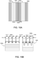
- FIGs. 15A and 15B are diagrams illustrating an example approach for implementation of a clamping inductance in a transistor circuit, such as the transistor circuits of FIGs. 10A-10B, 11A-11B , 12A-12B, 13A-13B and 14A-14B .
- FIG. 15A schematically illustrates a top view of a transistor circuit 1510 with resonant clamping, which can be included in the example implementations described herein.
- the transistor circuit 1510 includes a plurality of stripes of a clamping diode, e.g., a stripe 1532a, and a stripe 1532b.
- the stripe 1532a and the stripe 1532b can be interconnected, e.g., by an overlying metal layer (not shown in FIGs. 15A and 15B ), such as a source metal layer for a power MOSFET 1520 of the transistor circuit 1510.
- the power MOSFET 1520 also includes a plurality of stripes, indicated by gate trenches 1520s, which stripes can be interconnected (e.g., via the overlying source metal layer) to form the corresponding power MOSFET 1520.
- FIG. 15B which illustrates side, cross-sectional views of semiconductor structures of the portion of the transistor circuit 1510 indicated by the dashed line inset shown in FIG. 15A (e.g., including the stripe 1532a of the clamping diode, and a portion of the power MOSFET 1520).
- the semiconductor structures shown in FIG. 15B are similar to those of the transistor circuit 1010, the transistor circuit 1110, the transistor circuit 1210, the transistor circuit 1310 and the transistor circuit 1410 shown, respectively, in FIGs. 10B, 11B , 12B, 13B and 14B .
- those views are shown inverted from the views of FIGs. 10B, 11B , 12B, 13B and 14B (e.g., with respective back sides of the associated semiconductor die being at the bottoms of the structures in the view in FIG. 15B ).
- a clamping inductance 1534 of a resonant clamping circuit of the transistor circuit 1510 can be a distributed inductance, including a plurality of L cl_v inductances, a plurality of L cl_h inductances, and at least one L cl_int inductance, which can be aggregated as the clamping inductance 1534 (L cl ).
- the L cl_v inductances can be inductances that are associated with electrical contacts, e.g., anode contacts of the clamping diode and/or contacts to source diffusion (and a body region) of the power MOSFET 1520.
- the L cl_h inductances can be inductances that are associated with electrical interconnects between diode stripes and/or power MOSFET stripes (e.g., between anode contacts and/or between source contacts).
- the at least one L cl_int inductance can be an inductance(s) associated with electrical interconnects between a clamping diode (e.g., the stripe 1532a and/or the stripe 1532b) and the power MOSFET 1520.
- such interconnects can be intra-die (e.g., within a same semiconductor) or inter-die (e.g., between separate die that are co-packaged or separately packaged).
- FIG. 16 is a diagram illustrating an example of adjusting a clamping inductance of a transistor circuit.
- a portion of a transistor circuit 1610 is shown, where the transistor circuit 1610 is similar to the transistor circuit 1510 of FIGs. 15A and 15B .
- the illustrate portion of the transistor circuit 1610 includes a stripe 1632 of a clamping diode and a portion of a power MOSFET 1620 (e.g., a plurality of MOSFET stripes). Also shown in FIG.
- the overlying metal layer 1670 can include a plurality of openings 1675 (e.g., holes, slits, etc.) which can alter an associated inductance (L cl_int ) corresponding with the overlying metal layer 1670, e.g., as compared to a metal layer without such openings.
- openings 1675 e.g., holes, slits, etc.
- L cl_int an associated inductance
- a circuit in a general aspect, includes a metal-oxide semiconductor field-effect transistor (MOSFET) having a gate, a source, and a drain.
- MOSFET metal-oxide semiconductor field-effect transistor
- the MOSFET has a first breakdown voltage.
- the circuit also includes a clamping circuit coupled between the drain and the source.
- the clamping circuit including a diode having a second breakdown voltage that is less than the first breakdown voltage.
- a cathode of the diode is coupled with the drain of the MOSFET.
- the clamping circuit further includes an inductor having a first terminal coupled with an anode of the diode, and a second terminal coupled with the source of the MOSFET.
- Implementations can include one or more of the following features or aspects, alone or in combination.
- the clamping circuit can be configured to resonate when a voltage applied to the drain of the MOSFET exceeds a breakdown voltage of the diode.
- the clamping circuit can include a capacitor and a resistor that is coupled in series with the capacitor.
- the capacitor and the resistor can be coupled in parallel with the diode and the inductor.
- the resistor and the capacitor can be coupled in parallel with the diode, and coupled in series with the inductor.
- the clamping circuit can include a frequency-dependent resistor.
- the second terminal of the inductor can be coupled with the source of the MOSFET via the frequency-dependent resistor.
- the inductor can be a first inductor.
- the clamping circuit can include a resistive-inductive-capacitive (RLC) circuit having a capacitor, a resistor, and a second inductor.
- the capacitor, the resistor and the second inductor can be coupled in series with each other.
- the RLC circuit can be coupled in parallel with the diode and the first inductor.
- the MOSFET can be included in a first semiconductor die.
- the diode can be included in a second semiconductor die that is co-packaged with the first semiconductor die.
- the inductor can include inductance of an electrical interconnect between the first semiconductor die and the second semiconductor die.
- the circuit can be implemented in a semiconductor die.
- the diode can include a plurality of interconnected stripes.
- the MOSFET can include a plurality of interconnected stripes.
- the inductor can include inductance from at least one of an electrical contact to the anode of the diode, an electrical contact to a source of the MOSFET, an electrical connection between a first stripe and a second stripe of the plurality of interconnected stripes of the diode, an electrical connection between a first stripe and a second stripe of the plurality of interconnected stripes of the MOSFET, or an electrical connection between the anode of the diode and the source of the MOSFET.
- the circuit can be implemented in a semiconductor die.
- the semiconductor die can include a metal layer electrically coupling the source of the MOSFET with the anode of the diode.
- the metal layer can have an inductance included in the inductor.
- the metal layer can include a plurality of openings configured to adjust the inductance of the metal layer.
- a half-bridge circuit in another general aspect, includes a high-side transistor circuit and a low-side transistor circuit.
- the high-side transistor circuit includes a first metal-oxide semiconductor field-effect transistor (MOSFET) having a gate, a source, and a drain.
- the first MOSFET has a first breakdown voltage.
- the high-side transistor circuit also includes a first clamping circuit including a first diode having a second breakdown voltage that is less than the first breakdown voltage. A cathode of the first diode is coupled with the drain of the first MOSFET.
- the first clamping circuit further includes a first inductor having a first terminal coupled with an anode of the first diode, and a second terminal coupled with the source of the first MOSFET.
- the low-side transistor circuit includes a second MOSFET including a gate, a source, and a drain.
- the second MOSFET has a third breakdown voltage.
- the drain of the second MOSFET is coupled with the source of the first MOSFET.
- the low-side transistor circuit also includes a second clamping circuit including a second diode having a fourth breakdown voltage that is less than the third breakdown voltage.
- a cathode of the second diode is coupled with the drain of the second MOSFET.
- the second clamping circuit further includes a second inductor having a first terminal coupled with an anode of the first diode, and a second terminal coupled with the source of the second MOSFET.
- Implementations can include one or more of the following features or aspects, alone or in combination.
- the first clamping circuit can be configured to resonate when a voltage applied to the drain of the first MOSFET exceeds a breakdown voltage of the first diode.
- the second clamping circuit can be configured to resonate when a voltage applied to the drain of the second MOSFET exceeds a breakdown voltage of the second diode.
- the high-side transistor circuit can be implemented in a semiconductor die.
- the first diode can include a plurality of interconnected stripes.
- the first MOSFET can include a plurality of interconnected stripes.
- the first inductor can include inductance from at least one of an electrical contact to the anode of the first diode, an electrical contact to a source of the first MOSFET, an electrical connection between a first stripe and a second stripe of the plurality of interconnected stripes of the first diode, an electrical connection between a first stripe and a second stripe of the plurality of interconnected stripes of the first MOSFET, or an electrical connection between the anode of the first diode and the source of the first MOSFET.
- the low-side transistor circuit can be implemented in a semiconductor die.
- the second diode can include a plurality of interconnected stripes.
- the second MOSFET can include a plurality of interconnected stripes.
- the second inductor can include inductance from at least one of an electrical contact to the anode of the second diode, an electrical contact to a source of the second MOSFET, an electrical connection between a first stripe and a second stripe of the plurality of interconnected stripes of the second diode, an electrical connection between a first stripe and a second stripe of the plurality of interconnected stripes of the second MOSFET, or an electrical connection between the anode of the second diode and the source of the second MOSFET.
- a power converter circuit in another general aspect, includes an output impedance circuit, and a half-bridge circuit coupled with the output impedance circuit.
- the half-bridge circuit includes a high-side transistor circuit and a low-side transistor circuit.
- the high-side transistor circuit includes a first metal-oxide semiconductor field-effect transistor (MOSFET) having a gate, a source, and a drain.
- the first MOSFET has a first breakdown voltage.
- the high-side transistor circuit also includes a first clamping circuit including a first diode having a second breakdown voltage that is less than the first breakdown voltage. A cathode of the first diode is coupled with the drain of the first MOSFET.
- MOSFET metal-oxide semiconductor field-effect transistor
- the first clamping circuit further includes a first inductor having a first terminal coupled with an anode of the first diode, and a second terminal coupled with the source of the first MOSFET.
- the low-side transistor circuit includes a second MOSFET including a gate, a source, and a drain.
- the second MOSFET has a third breakdown voltage.
- the drain of the second MOSFET is coupled with the source of the first MOSFET.
- the low-side transistor circuit also includes a second clamping circuit including a second diode having a fourth breakdown voltage that is less than the third breakdown voltage.
- a cathode of the second diode is coupled with the drain of the second MOSFET.
- the second clamping circuit further includes a second inductor having a first terminal coupled with an anode of the first diode, and a second terminal coupled with the source of the second MOSFET.
- the power converter circuit can be a buck converter circuit.
- the output impedance circuit can include an output inductor having a first terminal coupled to a switching node of the half-bridge circuit, and a second terminal coupled to an output node of the power converter circuit.
- the output impedance circuit can include an output capacitor having a first terminal coupled with the output node of the power converter circuit, and a second terminal coupled with the source of the second MOSFET.
- the first clamping circuit can be configured to resonate when a voltage applied to the drain of the first MOSFET exceeds a breakdown voltage of the first diode.
- the second clamping circuit can be configured to resonate when a voltage applied to the drain of the second MOSFET exceeds a breakdown voltage of the second diode.
- the first inductor can be configured such that a resonance period of the first clamping circuit is less than an avalanche time of the first diode during operation of the power converter circuit.
- the second inductor can be configured such that a resonance period of the second clamping circuit is less than an avalanche time of the second diode during operation of the power converter circuit.
- the first inductor can have a first inductance and the second inductor can have a second inductance that is greater than the first inductance.
- the various apparatus and techniques described herein may be implemented using various semiconductor processing and/or packaging techniques. Some embodiments may be implemented using various types of semiconductor processing techniques associated with semiconductor substrates including, but not limited to, for example, Silicon (Si), Gallium Arsenide (GaAs), Silicon Carbide (SiC), and/or so forth.
- semiconductor substrates including, but not limited to, for example, Silicon (Si), Gallium Arsenide (GaAs), Silicon Carbide (SiC), and/or so forth.
- coupled to, or coupled with can refer to being electrically coupled to, electrically coupled with, physically coupled to, and/or physically coupled with.
Landscapes
- Engineering & Computer Science (AREA)
- Power Engineering (AREA)
- Dc-Dc Converters (AREA)
- Semiconductor Integrated Circuits (AREA)
Abstract

Description
- This description relates to semiconductor devices and, more particularly, to transistor circuits, such as field effect transistors implemented with a resonant clamping circuit, which can be used, e.g., in power converter circuits.
- Power transistors are used in a number of applications, such as consumer electronics, automotive electronics, industrial electronics, etc. For example, power transistors are used in power conversion circuits, such as direct-current to direct-current (DC-DC) power converters (e.g., synchronous buck converters, etc.), where a power output of the power converter is coupled to a switch node between a high-side (HS) transistor and a low-side (LS) transistor of half-bridge circuit included in a power converter. Voltage and current overshoot and/or ringing can occur, e.g., during switching of the half-bridge circuit. Such overshoot and/or ringing can cause a voltage on a power supply node and/or the switch node to exceed a respective breakdown voltage of the HS or LS transistor, such as a drain-to-source breakdown voltage (BVdss) of a vertical, trench-gate, power metal-oxide semiconductor field-effect transistor (MOSFET), e.g., breakdown voltage of a body diode of the MOSFET. When MOSFET BVdss is exceeded, power conversion efficiency of an associated power converter can be reduced and/or damage to the transistor can occur, such as threshold drift, breakdown voltage shift, structural damage, etc.
- One approach used to prevent such power efficiency loss and/or potential transistor damage, e.g., for a given implementation, is to increase BVdss of the transistors. However, increasing BVdss also increases on-state resistance of the transistors, such as drain-to-source on-state resistance (Rdson), which results in higher resistive losses, and also decreases power conversion efficiency.
- In a general aspect, a circuit includes a metal-oxide semiconductor field-effect transistor (MOSFET) having a gate, a source, and a drain. The MOSFET has a first breakdown voltage. The circuit also includes a clamping circuit coupled between the drain and the source. The clamping circuit including a diode having a second breakdown voltage that is less than the first breakdown voltage. A cathode of the diode is coupled with the drain of the MOSFET. The clamping circuit further includes an inductor having a first terminal coupled with an anode of the diode, and a second terminal coupled with the source of the MOSFET.
- In another general aspect, a half-bridge circuit includes a high-side transistor circuit and a low-side transistor circuit. The high-side transistor circuit includes a first metal-oxide semiconductor field-effect transistor (MOSFET) having a gate, a source, and a drain. The first MOSFET has a first breakdown voltage. The high-side transistor circuit also includes a first clamping circuit including a first diode having a second breakdown voltage that is less than the first breakdown voltage. A cathode of the first diode is coupled with the drain of the first MOSFET. The first clamping circuit further includes a first inductor having a first terminal coupled with an anode of the first diode, and a second terminal coupled with the source of the first MOSFET. The low-side transistor circuit includes a second MOSFET including a gate, a source, and a drain. The second MOSFET has a third breakdown voltage. The drain of the second MOSFET is coupled with the source of the first MOSFET. The low-side transistor circuit also includes a second clamping circuit including a second diode having a fourth breakdown voltage that is less than the third breakdown voltage. A cathode of the second diode is coupled with the drain of the second MOSFET. The second clamping circuit further includes a second inductor having a first terminal coupled with an anode of the first diode, and a second terminal coupled with the source of the second MOSFET.
- In another general aspect, a power converter circuit includes an output impedance circuit, and a half-bridge circuit coupled with the output impedance circuit. The half-bridge circuit includes a high-side transistor circuit and a low-side transistor circuit. The high-side transistor circuit includes a first metal-oxide semiconductor field-effect transistor (MOSFET) having a gate, a source, and a drain. The first MOSFET has a first breakdown voltage. The high-side transistor circuit also includes a first clamping circuit including a first diode having a second breakdown voltage that is less than the first breakdown voltage. A cathode of the first diode is coupled with the drain of the first MOSFET. The first clamping circuit further includes a first inductor having a first terminal coupled with an anode of the first diode, and a second terminal coupled with the source of the first MOSFET. The low-side transistor circuit includes a second MOSFET including a gate, a source, and a drain. The second MOSFET has a third breakdown voltage. The drain of the second MOSFET is coupled with the source of the first MOSFET. The low-side transistor circuit also includes a second clamping circuit including a second diode having a fourth breakdown voltage that is less than the third breakdown voltage. A cathode of the second diode is coupled with the drain of the second MOSFET. The second clamping circuit further includes a second inductor having a first terminal coupled with an anode of the first diode, and a second terminal coupled with the source of the second MOSFET.
-
-
FIG. 1 is a block diagram illustrating an example transistor circuit with a resonant clamping circuit. -
FIG. 2 is a block diagram illustrating an example power converter circuit including a half-bridge circuit that can be implemented using the transistor circuit ofFIG. 1 . -
FIG. 3 is a schematic diagram illustrating an example power converter circuit, which can implement the power converter circuit ofFIG. 2 . -
FIG. 4 is a graph comparing operation of an implementation of the transistor circuit ofFIG. 1 , as a high-side transistor, with a comparable transistor circuit with a non-resonant clamping circuit in a power converter circuit. -
FIG. 5 is a graph illustrating peak drain-to-source voltage versus clamping inductance for an implementation of the transistor circuit ofFIG. 1 as a high-side transistor. -
FIG. 6 is a graph illustrating change in power-conversion efficiency for an implementation of the transistor circuit ofFIG. 1 , as a high-side transistor, versus clamping inductance compared to efficiency of a comparable transistor circuit with a non-resonant clamping circuit. -
FIG. 7 is a graph comparing operation of an implementation of the transistor circuit ofFIG. 1 , as a low-side transistor, with a comparable transistor circuit with a non-resonant clamping circuit in a power converter circuit. -
FIG. 8 is a graph illustrating peak drain-to-source voltage versus clamping inductance for an implementation of the transistor circuit ofFIG. 1 as a low-side transistor. -
FIG. 9 is a graph illustrating power-use efficiency for an implementation of the transistor circuit ofFIG. 1 , as a low-side transistor, versus clamping inductance. -
FIGs. 10A and 10B are diagrams illustrating an example transistor circuit with resonant clamping, such as the transistor circuits of the power converter circuit ofFIG. 3 . -
FIGs. 11A and 11B are diagrams illustrating another example transistor circuit with resonant clamping. -
FIGs. 12A and 12B are diagrams illustrating another example transistor circuit with resonant clamping. -
FIGs. 13A and 13B are diagrams illustrating another example transistor circuit with resonant clamping. -
FIGs. 14A and 14B are diagrams illustrating another example transistor circuit with resonant clamping. -
FIGs. 15A and 15B are diagrams illustrating an example approach for implementation of a clamping inductance in a transistor circuit, such as the transistor circuit ofFIGs. 10A and 10B . -
FIG. 16 is a diagram illustrating an example of adjusting a clamping inductance of a transistor circuit. - In the drawings, which are not necessarily drawn to scale, like reference symbols may indicate like and/or similar components (elements, structures, etc.) in different views. The drawings illustrate generally, by way of example, but not by way of limitation, various implementations discussed in the present disclosure. Reference symbols shown in one drawing may not be repeated for the same, and/or similar elements in related views. Reference symbols that are repeated in multiple drawings may not be specifically discussed with respect to each of those drawings, but are provided for context between related views. Also, not all like elements in the drawings are specifically referenced with a reference symbol when multiple instances of an element are illustrated.
- In some implementations, approaches for reducing voltage and current ringing and/or overshoot in transistors included in power converter circuits, such as a synchronous buck direct-current to direct-current (DC-DC) power converters, include use of clamping diodes. For instance, in such implementations, respective clamping diodes are coupled in parallel with each of a high-side (HS) transistor and a low-side (LS) transistor of a half-bridge circuit included in the power converter circuit. Each clamping diode can be a diode with a breakdown voltage that is less than a breakdown voltage of an associated transistor. For instance, such a clamping diode can be configured to enter avalanche breakdown at voltage (BVka) that is lower than a voltage at which an associated transistor enters avalanche breakdown (BVdss).
- However, as the primary mechanism by which such clamping diodes reduce voltage and current overshoot and/or ringing is via periodic avalanche breakdown of the clamping diode, such approaches can result in an undesired loss of power conversion efficiency (e.g., due to power consumed during the periodic avalanche). Further, this periodic avalanche can result in drift of BVka of the clamping diode, which could result in increased power loss due to a reduction in BVka, or undesired avalanche occurring in an associated transistor due to an increase in BVka. Accordingly, such BVka drift can further impact efficiency of the associated power converter, as well as long term reliability of the associated transistor or transistors, e.g., LS and/or HS trench-gate, vertical power metal-oxide-semiconductor field-effect transistors (MOSFETs), as well as associated circuitry of the power converter, such as drivers, controllers, etc.
- This disclosure is directed to implementations that address at least some of the concerns noted above (e.g., loss of efficiency, BVka drift, long term reliability issues). For instance, the implementations described herein provide for affecting discontinuous avalanche in clamping diodes, such as clamping diodes included in HS transistor circuits and/or LS transistor circuits, such the example implementations described herein. This discontinuous avalanche is achieved by inducing resonance in a corresponding clamping diode voltage (Vka) and corresponding clamping diode current (Ika), e.g., during avalanche of the clamping diode. In example implementations, this resonance is induced (affected, produced, etc.) using at least one inductance (e.g., an inductor, an aggregate of a plurality of distributed inductances, etc.) that is coupled in series with the clamping diode, and in parallel with the corresponding transistor. That is, in some implementations, such as those described herein, a clamping circuit for a HS transistor or a LS transistor can include a clamping diode in series with at least one clamping inductance, where the series coupled diode and inductance are coupled in parallel with an associated transistor (e.g., between a source terminal and a drain terminal of the transistor).
-
FIG. 1 is a block diagram illustrating anexample transistor circuit 110 with a resonant clamping circuit. As shown inFIG. 1 , thetransistor circuit 110 includes apower MOSFET 120 and aresonant clamping circuit 130. In some implementations, thepower MOSFET 120 can be a vertical, trench-gate MOSFET, such as an n-channel, power MOSFET. In some implementations, thetransistor circuit 110 can be included in a power converter. For instance, respective implementations of thetransistor circuit 110 can be included in a power converter as a HS transistor circuit of a corresponding half-bridge circuit, and a LS transistor circuit of the corresponding half-bridge circuit. As noted above, in some implementations, theresonant clamping circuit 130 can include a series coupled diode and inductance (an LD circuit), where the LD circuit is coupled in parallel with thepower MOSFET 120, e.g., between a source terminal and a drain terminal of thepower MOSFET 120. Example implementations of thetransistor circuit 110 are illustrated and described below with respect to, at least,FIGs. 3 ,10A-10B ,11A-11B ,12A-12B ,13A-13B and14A-14B . - In some implementations, the
power MOSFET 120 and theresonant clamping circuit 130 can be implemented in a single semiconductor die. In other implementations, thetransistor circuit 110 can be implemented in a first semiconductor die, while at least a clamping diode of theresonant clamping circuit 130 can be implemented in a second die. In this example, inductance of theresonant clamping circuit 130 can include, at least, inductance associated with electrical interconnects between the first semiconductor die and the second semiconductor die. For instance, the first semiconductor die and the second semiconductor die can be co-packaged (as multi-chip module in a single package assembly). Interconnects, such as conductive clips, wire bonds, etc., between the first semiconductor die and the second semiconductor die can be configured to provide, at least in part, an inductance of an associated resonant clamping circuit. -
FIG. 2 is a block diagram illustrating an examplepower converter circuit 200 that includes a half-bridge circuit 215. In this example, the half-bridge circuit 215 can be implemented using thetransistor circuit 110 ofFIG. 1 . That is, the half-bridge circuit 215 of thepower converter circuit 200 can include respective implementations of thetransistor circuit 110 for a HS transistor and a LS transistor of the half-bridge circuit 215. For instance, in thepower converter circuit 200, each of a LS transistor circuit and a HS transistor circuit of the half-bridge circuit 215 can include a corresponding resonant clamping circuit, such as those described herein. For instance, the half-bridge circuit 215 can be implemented using one or more of the example transistor circuits described and illustrated herein, such as the examples of, at least,FIGs. 3 ,10A-10B, 11A-11B ,12A-12B, 13A-13B and14A-14B . - The
power converter circuit 200, as shown inFIG. 2 , also includes anoutput impedance circuit 240, which can be an inductive-capacitive circuit (LC circuit) for achieving power conversion, e.g., DC-DC conversion, based on a signal generated (provided, produced, etc.) on a switching node of the half-bridge circuit 215. For instance, the signal provided on the switching node can be an alternating current signal produced by the half-bridge circuit 215 from an input DC voltage signal. In this example, thepower converter circuit 200 can be a synchronous buck converter, though, in some implementations, thepower converter circuit 200 can implement other types of power converters, such as boost converters. -
FIG. 3 is a schematic diagram illustrating an examplepower converter circuit 300, which can be an implementation of thepower converter circuit 200 ofFIG. 2 . As shown inFIG. 3 , thepower converter circuit 300 includes aninput capacitance 305, an inductor 307, a HS transistor circuit 310hs, a LS transistor circuit 3101s, a switching node 317 (disposed between the HS transistor circuit 310hs and the LS transistor circuit 3101s), and anoutput impedance circuit 340. In this example, theinput capacitance 305 can include capacitance of the HS transistor circuit 310hs and the LS transistor circuit 310ls, as well as capacitance of a main power loop of thepower converter circuit 300. In this example, the inductor 307 can include a stray inductance of the main power loop of thepower converter circuit 300. - As shown in
FIG. 3 , the HS transistor circuit 310hs includes a transistor 320hs (with a corresponding body diode shown) and a resonant clamping circuit 330hs, while the LS transistor circuit 310ls includes a transistor 320ls (with a corresponding body diode shown) and a resonant clamping circuit 330ls. In this example, the transistor 320hs and the transistor 320ls can be respective vertical, trench-gate MOSFETs. Also in this example, the resonant clamping circuit 330hs and the resonant clamping circuit 330ls can be respective LD circuits (e.g., series coupled diode and inductance). Further in thepower converter circuit 300, theoutput impedance circuit 340 includes aninductor 342 and acapacitor 344, which are configured to provide a desired DC-DC power conversion ratio, e.g., step down of an input DC voltage to a desired output DC voltage. -
FIG. 4 is agraph 400 comparing operation of an implementation of the transistor circuit ofFIG. 1 , such as the HS transistor circuit 310hs ofFIG. 3 , with a comparable transistor circuit with a non-resonant clamping circuit (e.g., clamping diode only), when implemented as a HS transistor circuit in a power converter circuit (e.g., the power converter circuit 300). InFIG, 4 , time is indicated on the x-axis (increasing left to right), while drain-to-source voltage Vds of the HS transistor is indicated on the y-axis (increasing bottom to top). The values in thegraph 400 are normalized, and the specific values of time and Vds will depend on the particular implementation. - In the
graph 400, the dashedline 435 indicates a BVka of respective clamping diodes of the example transistor circuits illustrated in thegraph 400. Thetrace 450 illustrates Vds for a transistor circuit with a non-resonant clamping circuit, and thetrace 460 illustrates Vds for a transistor circuit with a resonant clamping circuit, e.g., the HS transistor circuit 310hs of thepower converter circuit 300 with a fixed clamping inductance. A value of the clamping inductance in this example will depend on the particular implementation. In some implementations, a clamping inductance of a HS transistor circuit, such as the HS transistor circuit 310hs, can be in a range of 0.01 nanohenries (nH) to 1 nH. - As can be seen by a comparison of the
trace 450 with thetrace 460, for the transistor circuit with a non-resonant clamping circuit (trace 450), an associated clamping diode operates in avalanche for the period of time from t0 to ti, as is indicated by Vds (which corresponds with Vka and Ika). In comparison, the transistor circuit with a resonant clamping circuit (trace 460), due to the induced resonance of Vds (via induced resonance of Vka and Ika), operates in avalanche approximately half of the period of time from t0 to t1. This reduction in the amount of time of periodic avalanche for the transistor circuit associated with the trace 460 (e.g., repeatedly over an operation period of an associated power converter circuit) can improve power conversion efficiency (e.g., a ratio of output power to input power), as well as reduce detrimental effects, such as BVka shift, avalanche occurring in the HS transistor, etc. -
FIG. 5 is agraph 500 illustrating peak Vds versus clamping inductance for an implementation of the transistor circuit ofFIG. 1 as a high-side transistor circuit, such as for the HS transistor circuit 310hs of thepower converter circuit 300 shown inFIG. 3 . That is, in thegraph 500, values of clamping inductance are indicated on the x-axis (increasing left to right), while corresponding peak Vds values are indicated on the y-axis (increasing bottom to top). The values in thegraph 500 are normalized, and the specific values of clamping inductance and peak Vds will depend on the particular implementation. As shown inFIG. 5 increasing clamping inductance for a HS transistor circuit results in corresponding increases in peak Vds. Accordingly, the value of the clamping inductance for a HS transistor circuit in this example (e.g., a synchronous buck converter, such as the power converter circuit 300) should be tuned (configured, adjusted, etc.) such that a corresponding peak Vds value does not result in continuous avalanche (e.g.,trace 450 inFIG. 4 ) occurring in a corresponding HS transistor during operation of the power converter circuit. -
FIG. 6 is agraph 600 illustrating changes in power-conversion efficiency (Δ Efficiency) versus HS clamping inductance for a power conversion circuit including an implementation of the transistor circuit ofFIG. 1 , e.g., as a HS transistor circuit. In this example, Δ Efficiency illustrated by thegraph 600 is as compared to power-conversion efficiency of a comparable power conversion circuit with a HS transistor circuit with a non-resonant clamping circuit. That is, in thegraph 600, values of clamping inductance are indicated on the x-axis (increasing left to right), while corresponding Δ Efficiency values are indicated on the y-axis. The clamping inductance values in thegraph 600 are normalized, and the specific values of clamping inductance will depend on the particular implementation. The x-axis scale in thegraph 600 is normalized to be consistent with the x-axis scale ofFIG. 5 . As can be seen from thegraph 500 and thegraph 600, increasing clamping inductance for the HS transistor circuit in this example provides small increases in Δ Efficiency (versus use of a non-resonant clamping circuit) while increasing peak Vds. Accordingly, any efficiency benefit associated with an increased HS clamping inductance may be outweighed by a corresponding increase in peak Vds. -
FIG. 7 is a graph comparing operation of an implementation of the transistor circuit ofFIG. 1 , such as the LS transistor circuit 310ls ofFIG. 3 , with a comparable transistor circuit with a non-resonant clamping circuit (e.g., clamping diode only), when implemented as a LS transistor circuit in a power converter circuit (e.g., the power converter circuit 300). InFIG, 7 , time is indicated on the x-axis (increasing left to right), while Vds of the LS transistor is indicated on the y-axis (increasing bottom to top). The values in the graph ofFIG. 7 are normalized, and the specific values of time and Vds will depend on the particular implementation. - In the graph of
FIG. 7 , the dashedline 735 indicates a BVka of respective clamping diodes of the example transistor circuits illustrated. Thetrace 750 illustrates Vds for a transistor circuit with a non-resonant clamping circuit, and thetrace 760 illustrates Vds for a transistor circuit with a resonant clamping circuit, e.g., the LS transistor circuit 310ls of thepower converter circuit 300 with a fixed clamping inductance. A value of the clamping inductance in this example will depend on the particular implementation. In some implementations, a clamping inductance of a LS transistor circuit, such as the LS transistor circuit 310ls, can be in a range of 0.01 nanohenries (nH) to 1 nH. That is, in some implementations, such as those described herein, a clamping inductance that is implemented for a LS transistor circuit can be larger (e.g., 4-5 time larger) than a clamping inductance implemented for a corresponding HS transistor circuit. This difference can be due, at least in part, to HS transistors and LS side transistors being sized differently in a power conversion circuit. e.g., a larger transistor (e.g., higher current capacity with associated higher capacitance) being used for a LS transistor circuit than a relatively smaller transistor that is used for implementing a corresponding HS transistor circuit. - As can be seen by a comparison of the
trace 750 with thetrace 760, for the transistor circuit with a non-resonant clamping circuit (trace 750), an associated clamping diode operates in avalanche for the period of time from t2 to t3, as is indicated by Vds (which corresponds with Vka and Ika). In comparison, the transistor circuit with a resonant clamping circuit (trace 760), due to the induced resonance of Vds (via induced resonance of Vka and Ika), operates in avalanche approximately half of the period of time from t2 to t3. As was discussed above with respect toFIG. 4 , this reduction in the amount of time of periodic avalanche for the transistor circuit associated with the trace 760 (e.g., repeatedly over an operation period of an associated power converter circuit) can improve power conversion efficiency (e.g., a ratio of output power to input power), as well as reduce detrimental effects, such as BVka shift, avalanche occurring in the HS transistor, etc. -
FIG. 8 is a graph illustrating peak Vds versus clamping inductance for an implementation of the transistor circuit ofFIG. 1 as a LS transistor circuit, such as for the LS transistor circuit 310ls of thepower converter circuit 300 shown inFIG. 3 . That is, in the graph ofFIG. 8 , values of clamping inductance are indicated on the x-axis (increasing left to right), while corresponding peak Vds values are indicated on the y-axis (increasing bottom to top). The values inFIG. 8 are normalized, and the specific values of clamping inductance and peak Vds will depend on the particular implementation. As shown inFIG. 8 , increasing clamping inductance for a LS transistor circuit initially results in corresponding increases in peak Vds and then, at a clamping inductance of approximately Lcl_ls, a decrease in peak Vds occurs. Accordingly, the value of the clamping inductance for a LS transistor circuit in this example (e.g., a synchronous buck converter, such as the power converter circuit 300) can be tuned (configured, adjusted, etc.) so as to benefit from such a decrease in a corresponding peak Vds value. As shown inFIG. 8 , some variation in peak Vds can be observed. Such variation can be due to interference between a signal in a circuit loop including a clamping diode, a clamping inductance and Coss of a MOSFET, and a signal in a main power loop. That is, when varying a value of the clamping inductance (Lcl), peak Vds can fluctuate due to such interference changing from constructive to destructive and vice versa. -
FIG. 9 is a graph illustrating power-conversion efficiency (percentage conversion efficiency) versus LS clamping inductance for a power conversion circuit including an implementation of the transistor circuit ofFIG. 1 , e.g., as a LS transistor circuit. In this example, power-conversion efficiency (in percentage), as illustrated by the graph inFIG. 9 , does not significantly change as a LS clamping inductance is increased. For instance, as shown inFIG. 9 , an approximately 0.2% variation was observed over the illustrated range, which covers more than three orders of magnitude of variation in LS clamping inductance. Accordingly, the benefit of reduced peak Vds associated with an increased LS clamping inductance does not cause a significant change (e.g., decrease) in associated power conversion efficiency. - In addition to the above discussed considerations (e.g., efficiency and peak Vds), resonance period should also be considered with selecting clamping inductance values for resonant clamping circuits. For instance, clamping inductance values should be selected such that a period of resonance (TRES) of an associated clamping circuit is less than an avalanche time TAVALANCHE for a corresponding clamping diode.
- Referring to the
power converter circuit 300 ofFIG. 3 as an example, in some implementations, e.g., where respective output capacitances of the clamping diodes of the HS transistor circuit 310hs and the LS transistor circuit 310ls are negligible as compared to respective output capacitances Coss of the corresponding HS transistor 320hs and the corresponding LS transistor 320ls, TRES can be given by:
- Further in this example, due to the sizing of the HS transistor 320hs as compared to the sizing of the LS transistor 320ls, as well as their arrangement in the
power converter circuit 300, calculation of the avalanche time for each of the HS transistor circuit 310hs and the LS transistor circuit 310ls is significantly different. For instance, avalanche time for the LS transistor circuit 310ls can be given (approximately) by:
- Avalanche time for the HS transistor circuit 310hs can be given by:

power converter circuit 300, α is a factor indicating a percentage of ILOAD that is avalanche current, BVKA is the breakdown (avalanche) voltage of the HS clamping diode, and VIN is the input voltage of the power converter circuit 300 (e.g., the voltage being converted). Accordingly, to achieve desired values of TRES for the HS transistor circuit 310hs and the LS transistor circuit 310ls, different values of clamping inductance may be used, e.g., based on the foregoing provided equations. - Example implementations of various transistor circuits with resonant clamping circuits (e.g., implementations of the transistor circuit 110) are respectively illustrated in
FIGs. 10A-10B, 11A-11B ,12A-12B, 13A-13B and14A-14B . Each of these respective implementations is illustrated as a circuit schematic (FIGs. 10A, 11A ,12A, 13A and14A ), and as a hybrid diagram including circuit schematic elements in combination with cross-sectional semiconductor device views (FIGs. 10B, 11B ,12B, 13B and14B ). Each of the illustrated example transistor circuits includes a MOSFET, a clamping diode and at least one clamping inductance. Some of the example implementations also include a resistor and/or a capacitor in their resonant clamping circuit. Various approaches can be used for implementing these elements. For instance, in some implementations, clamping inductances can include inductance from different metal structures, such as contacts, electrical interconnects, and/or other structures, such as metal spirals formed in a semiconductor device. In some implementations, resistors can be implemented using polysilicon structures, diffusion structures, metal structures, etc. In some implementations, capacitors can be implemented using polysilicon electrodes disposed in dielectric lined trenches that are formed in highly doped semiconductor regions, or can be implemented with a dielectric (e.g., oxide) disposed between two conductive plates (e.g., metal plate and/or doped polysilicon plates). The foregoing are provided by way of example, and other approaches for implementing the elements of the example transistor circuits ofFIGs. 10A-10B, 11A-11B ,12A-12B, 13A-13B and14A-14B are possible. - Also, for purposes of illustration and by way of example, same semiconductor device structures (clamping diode and trench-gate MOSFET structures) are illustrated in the hybrid diagrams of
FIGs. 10B, 11B ,12B, 13B and14B . In some implementations, structures other than those illustrated could be used. Further, certain aspects of the MOSFET (e.g., gate, source and drain terminals) and the clamping diode (anode and cathode) of the example transistor circuits are referenced in, and discussed with respect toFIGs. 10A and 10B . However, for purposes of brevity and clarity, these elements may not be specifically referenced and/or described with respect to the other example transistor circuit implementations ofFIGs. 11A-11B ,12A-12B, 13A-13B and14A-14B . -
FIGs. 10A and 10B are diagrams illustrating anexample transistor circuit 1010 with resonant clamping, such as the transistor circuits (HS transistor circuit 310hs and LS transistor circuit 310ls) of thepower converter circuit 300 ofFIG. 3 . As shown inFIGs. 10A and 10B , thetransistor circuit 1010 includes apower MOSFET 1020 and aresonant clamping circuit 1030. Thepower MOSFET 1020 includes agate terminal 1020g, adrain terminal 1020d and asource terminal 1020s, which are referenced in bothFIGs. 10A and 10B . As discussed herein, thepower MOSFET 1020 can be a vertical, trench-gate MOSFET, as shown by the cross-sectional semiconductor structure view ofFIG. 10B . As further shown in inFIGs. 10A and 10B , theresonant clamping circuit 1030 includes aclamping diode 1032 and aclamping inductance 1034, which are coupled in series with one another. That is, a first terminal of theclamping inductance 1034 is coupled with the source terminal 1020s of thepower MOSFET 1020, while a second terminal of theclamping inductance 1034 is coupled with ananode terminal 1032a of theclamping diode 1032. - As also shown in
FIGs. 10A and 10B , acathode terminal 1032c of theclamping diode 1032 is coupled with thedrain terminal 1020d of thepower MOSFET 1020. That is, the series coupled clampingdiode 1032 and clampinginductance 1034 of theresonant clamping circuit 1030 are coupled in parallel with thepower MOSFET 1020. As shown inFIG. 10B , the clampingdiode 1032 can be implemented with theanode terminal 1032a being a heavily doped p-type region disposed on thecathode terminal 1032c that is implemented by an n-type region (e.g., and epitaxially formed region). It is noted that inFIG 10B (as well asFIGs. 11B ,12B ,13B and14B ) the cross-sectional views of the corresponding clamping diodes and the MOSFETs are shown inverted. That is, in these diagrams, back sides (bottom sides) of a corresponding semiconductor die (or separate die) are shown at respective tops of the structures in the illustrated views. -
FIGs. 11A and 11B are diagrams illustrating anotherexample transistor circuit 1110 with resonant clamping. As with thetransistor circuit 1010, thetransistor circuit 1110 includes apower MOSFET 1120, and aresonant clamping circuit 1130, including aclamping diode 1132 and aclamping inductance 1134, which are connected in a same arrangement as the corresponding elements of thetransistor circuit 1010. Accordingly, for purposes of brevity, those like elements are not described in detail again with respect toFIGs. 11A and 11B . - In addition to the above elements, the
transistor circuit 1110 includes a resistive-capacitive (RC) circuit branch that is connected in parallel with the power MOSFET 1120 (as well as in parallel with the LD circuit including theclamping diode 1132 and the clamping inductance 1134). As shown inFIGs. 11A and 11B , the RC circuit branch can include acapacitor 1136 and aresistor 1138. Thecapacitor 1136, as shown inFIG. 11B , can be implemented by a polysilicon electrode that is disposed in a dielectric lined trench included at an edge of theclamping diode 1132. Theresistor 1138 can be implemented, at least in part, by a resistance of the poly electrode of thecapacitor 1136. In this example, the RC circuit branch can modulate resonance of theresonant clamping circuit 1130. -
FIGs. 12A and 12B are diagrams illustrating anotherexample transistor circuit 1210 with resonant clamping. As with thetransistor circuit 1010 and thetransistor circuit 1110, thetransistor circuit 1210 includes apower MOSFET 1220, and aresonant clamping circuit 1230, including aclamping diode 1232 and aclamping inductance 1234, which are connected in a same arrangement as the corresponding elements of thetransistor circuit 1010 and thetransistor circuit 1110. Accordingly, for purposes of brevity, those like elements are not described in detail again with respect toFIGs. 12A and 12B . - In addition to the above elements, the
transistor circuit 1210 includes a resistive-capacitive (RC) circuit branch that is connected in parallel with theclamping diode 1232, and in series with theclamping inductance 1234. As shown inFIGs. 12A and 12B , the RC circuit branch can include acapacitor 1236 and aresistor 1238. Thecapacitor 1236, as shown inFIG. 12B , as with thecapacitor 1136, can be implemented by a polysilicon electrode that is disposed in a dielectric lined trench included at an edge of theclamping diode 1232. Theresistor 1238, as with theresistor 1138, can be implemented, at least in part, by a resistance of the poly electrode of thecapacitor 1236. In this example, as with the RC circuit branch of thetransistor circuit 1110, the RC circuit branch of thetransistor circuit 1210 can modulate resonance of theresonant clamping circuit 1230. -
FIGs. 13A and 13B are diagrams illustrating anotherexample transistor circuit 1310 with resonant clamping. As with thetransistor circuit 1010, thetransistor circuit 1110, and thetransistor circuit 1210, thetransistor circuit 1310 includes apower MOSFET 1320, and aresonant clamping circuit 1330, including aclamping diode 1332 and aclamping inductance 1334, which are connected in a same arrangement as the corresponding elements of thetransistor circuit 1010, thetransistor circuit 1110, and thetransistor circuit 1210. Accordingly, for purposes of brevity, those like elements are not described in detail again with respect toFIGs. 13A and 13B . - In addition to the above elements, the
transistor circuit 1210 includes a frequency-dependent resistor 1338 that is coupled in series with theclamping diode 1332 and theclamping inductance 1334. In this example, the frequency-dependent resistor 1338 can provide resonance damping for theresonant clamping circuit 1330 of thetransistor circuit 1310. In some implementations, the frequency-dependent resistor 1338 can be implemented, e.g., using metal vias with a thickness and width engineered to enhance a skin effect and, as a result, a resistance dependence with frequency. -
FIGs. 14A and 14B are diagrams illustrating anotherexample transistor circuit 1410 with resonant clamping. As with thetransistor circuit 1010, thetransistor circuit 1110, thetransistor circuit 1210, and thetransistor circuit 1310, thetransistor circuit 1410 includes apower MOSFET 1420, and aresonant clamping circuit 1430, including aclamping diode 1432 and aclamping inductance 1434, which are connected in a same arrangement as the corresponding elements of thetransistor circuit 1010, thetransistor circuit 1110, thetransistor circuit 1210, and thetransistor circuit 1310. Accordingly, for purposes of brevity, those like elements are not described in detail again with respect toFIGs. 14A and 14B . - In addition to the above elements, the
transistor circuit 1410 includes a resistive-inductive-capacitive (RLC) circuit branch that is connected in parallel with the power MOSFET 1420 (as well as in parallel with the LD circuit including theclamping diode 1432 and the clamping inductance 1434). As shown inFIGs. 14A a14B , the RLC circuit branch can include acapacitor 1436, aresistor 1438, and aninductor 1439. The elements of the RLC circuit branch of thetransistor circuit 1410 can be implemented, for example, using the approaches describe herein. For instance, thecapacitor 1436, as shown inFIG. 14B , can be implemented by a polysilicon electrode that is disposed in a dielectric lined trench included at an edge of theclamping diode 1432. Theresistor 1438 can be implemented, at least in part, by a resistance of the poly electrode of thecapacitor 1136. Theinductor 1439 can be implemented using inductance of, e.g., one or more metal structures, such as using the approaches described herein. In this example, the RLC circuit branch can provide resonance damping and/or resonance modulation for theresonant clamping circuit 1430. In some implementations, theinductor 1439 can have an inductance that is greater than the inductance of theinductor 1434. -
FIGs. 15A and 15B are diagrams illustrating an example approach for implementation of a clamping inductance in a transistor circuit, such as the transistor circuits ofFIGs. 10A-10B, 11A-11B ,12A-12B, 13A-13B and14A-14B .FIG. 15A schematically illustrates a top view of atransistor circuit 1510 with resonant clamping, which can be included in the example implementations described herein. As shown inFIG. 15A , thetransistor circuit 1510 includes a plurality of stripes of a clamping diode, e.g., astripe 1532a, and astripe 1532b. In this example, thestripe 1532a and thestripe 1532b can be interconnected, e.g., by an overlying metal layer (not shown inFIGs. 15A and 15B ), such as a source metal layer for apower MOSFET 1520 of thetransistor circuit 1510. In this example, thepower MOSFET 1520 also includes a plurality of stripes, indicated bygate trenches 1520s, which stripes can be interconnected (e.g., via the overlying source metal layer) to form thecorresponding power MOSFET 1520. - As shown in
FIG. 15B , which illustrates side, cross-sectional views of semiconductor structures of the portion of thetransistor circuit 1510 indicated by the dashed line inset shown inFIG. 15A (e.g., including thestripe 1532a of the clamping diode, and a portion of the power MOSFET 1520). The semiconductor structures shown inFIG. 15B are similar to those of thetransistor circuit 1010, thetransistor circuit 1110, thetransistor circuit 1210, thetransistor circuit 1310 and thetransistor circuit 1410 shown, respectively, inFIGs. 10B, 11B ,12B, 13B and14B . However, in the view ofFIG. 15B , those views are shown inverted from the views ofFIGs. 10B, 11B ,12B, 13B and14B (e.g., with respective back sides of the associated semiconductor die being at the bottoms of the structures in the view inFIG. 15B ). - As shown in
FIG. 15B , aclamping inductance 1534 of a resonant clamping circuit of thetransistor circuit 1510 can be a distributed inductance, including a plurality of Lcl_v inductances, a plurality of Lcl_h inductances, and at least one Lcl_int inductance, which can be aggregated as the clamping inductance 1534 (Lcl). In some implementations, the Lcl_v inductances can be inductances that are associated with electrical contacts, e.g., anode contacts of the clamping diode and/or contacts to source diffusion (and a body region) of thepower MOSFET 1520. Further, the Lcl_h inductances can be inductances that are associated with electrical interconnects between diode stripes and/or power MOSFET stripes (e.g., between anode contacts and/or between source contacts). Still further, the at least one Lcl_int inductance can be an inductance(s) associated with electrical interconnects between a clamping diode (e.g., thestripe 1532a and/or thestripe 1532b) and thepower MOSFET 1520. For instance, such interconnects can be intra-die (e.g., within a same semiconductor) or inter-die (e.g., between separate die that are co-packaged or separately packaged). -
FIG. 16 is a diagram illustrating an example of adjusting a clamping inductance of a transistor circuit. In the example ofFIG. 16 , a portion of atransistor circuit 1610 is shown, where thetransistor circuit 1610 is similar to thetransistor circuit 1510 ofFIGs. 15A and 15B . For instance, in the view ofFIG. 16 , the illustrate portion of thetransistor circuit 1610 includes astripe 1632 of a clamping diode and a portion of a power MOSFET 1620 (e.g., a plurality of MOSFET stripes). Also shown inFIG. 16 is an overlying metal layer 1670 (e.g., source metal layer for the power MOSFET 1620), which can interconnect thestripe 1632 with thepower MOSFET 1620, and can have an inductance corresponding with the at least one Lcl_int of thetransistor circuit 1510 ofFIGs. 15A and 15B . As shown inFIG. 16 , the overlyingmetal layer 1670 can include a plurality of openings 1675 (e.g., holes, slits, etc.) which can alter an associated inductance (Lcl_int) corresponding with the overlyingmetal layer 1670, e.g., as compared to a metal layer without such openings. Of course, other approaches for adjusting (tuning, modifying, achieving, etc.) a clamping inductance of a resonant clamping circuit are possible. - In a general aspect, a circuit includes a metal-oxide semiconductor field-effect transistor (MOSFET) having a gate, a source, and a drain. The MOSFET has a first breakdown voltage. The circuit also includes a clamping circuit coupled between the drain and the source. The clamping circuit including a diode having a second breakdown voltage that is less than the first breakdown voltage. A cathode of the diode is coupled with the drain of the MOSFET. The clamping circuit further includes an inductor having a first terminal coupled with an anode of the diode, and a second terminal coupled with the source of the MOSFET.
- Implementations can include one or more of the following features or aspects, alone or in combination. For example, the clamping circuit can be configured to resonate when a voltage applied to the drain of the MOSFET exceeds a breakdown voltage of the diode.
- The clamping circuit can include a capacitor and a resistor that is coupled in series with the capacitor. The capacitor and the resistor can be coupled in parallel with the diode and the inductor. The resistor and the capacitor can be coupled in parallel with the diode, and coupled in series with the inductor.
- The clamping circuit can include a frequency-dependent resistor. The second terminal of the inductor can be coupled with the source of the MOSFET via the frequency-dependent resistor.
- The inductor can be a first inductor. The clamping circuit can include a resistive-inductive-capacitive (RLC) circuit having a capacitor, a resistor, and a second inductor. The capacitor, the resistor and the second inductor can be coupled in series with each other. The RLC circuit can be coupled in parallel with the diode and the first inductor.
- The MOSFET can be included in a first semiconductor die. The diode can be included in a second semiconductor die that is co-packaged with the first semiconductor die. The inductor can include inductance of an electrical interconnect between the first semiconductor die and the second semiconductor die.
- The circuit can be implemented in a semiconductor die. The diode can include a plurality of interconnected stripes. The MOSFET can include a plurality of interconnected stripes. The inductor can include inductance from at least one of an electrical contact to the anode of the diode, an electrical contact to a source of the MOSFET, an electrical connection between a first stripe and a second stripe of the plurality of interconnected stripes of the diode, an electrical connection between a first stripe and a second stripe of the plurality of interconnected stripes of the MOSFET, or an electrical connection between the anode of the diode and the source of the MOSFET.
- The circuit can be implemented in a semiconductor die. The semiconductor die can include a metal layer electrically coupling the source of the MOSFET with the anode of the diode. The metal layer can have an inductance included in the inductor. The metal layer can include a plurality of openings configured to adjust the inductance of the metal layer.
- In another general aspect, a half-bridge circuit includes a high-side transistor circuit and a low-side transistor circuit. The high-side transistor circuit includes a first metal-oxide semiconductor field-effect transistor (MOSFET) having a gate, a source, and a drain. The first MOSFET has a first breakdown voltage. The high-side transistor circuit also includes a first clamping circuit including a first diode having a second breakdown voltage that is less than the first breakdown voltage. A cathode of the first diode is coupled with the drain of the first MOSFET. The first clamping circuit further includes a first inductor having a first terminal coupled with an anode of the first diode, and a second terminal coupled with the source of the first MOSFET. The low-side transistor circuit includes a second MOSFET including a gate, a source, and a drain. The second MOSFET has a third breakdown voltage. The drain of the second MOSFET is coupled with the source of the first MOSFET. The low-side transistor circuit also includes a second clamping circuit including a second diode having a fourth breakdown voltage that is less than the third breakdown voltage. A cathode of the second diode is coupled with the drain of the second MOSFET. The second clamping circuit further includes a second inductor having a first terminal coupled with an anode of the first diode, and a second terminal coupled with the source of the second MOSFET.
- Implementations can include one or more of the following features or aspects, alone or in combination. For example, the first clamping circuit can be configured to resonate when a voltage applied to the drain of the first MOSFET exceeds a breakdown voltage of the first diode. The second clamping circuit can be configured to resonate when a voltage applied to the drain of the second MOSFET exceeds a breakdown voltage of the second diode.
- The high-side transistor circuit can be implemented in a semiconductor die. The first diode can include a plurality of interconnected stripes. The first MOSFET can include a plurality of interconnected stripes. The first inductor can include inductance from at least one of an electrical contact to the anode of the first diode, an electrical contact to a source of the first MOSFET, an electrical connection between a first stripe and a second stripe of the plurality of interconnected stripes of the first diode, an electrical connection between a first stripe and a second stripe of the plurality of interconnected stripes of the first MOSFET, or an electrical connection between the anode of the first diode and the source of the first MOSFET.
- The low-side transistor circuit can be implemented in a semiconductor die. The second diode can include a plurality of interconnected stripes. The second MOSFET can include a plurality of interconnected stripes. The second inductor can include inductance from at least one of an electrical contact to the anode of the second diode, an electrical contact to a source of the second MOSFET, an electrical connection between a first stripe and a second stripe of the plurality of interconnected stripes of the second diode, an electrical connection between a first stripe and a second stripe of the plurality of interconnected stripes of the second MOSFET, or an electrical connection between the anode of the second diode and the source of the second MOSFET.
- In another general aspect, a power converter circuit includes an output impedance circuit, and a half-bridge circuit coupled with the output impedance circuit. The half-bridge circuit includes a high-side transistor circuit and a low-side transistor circuit. The high-side transistor circuit includes a first metal-oxide semiconductor field-effect transistor (MOSFET) having a gate, a source, and a drain. The first MOSFET has a first breakdown voltage. The high-side transistor circuit also includes a first clamping circuit including a first diode having a second breakdown voltage that is less than the first breakdown voltage. A cathode of the first diode is coupled with the drain of the first MOSFET. The first clamping circuit further includes a first inductor having a first terminal coupled with an anode of the first diode, and a second terminal coupled with the source of the first MOSFET. The low-side transistor circuit includes a second MOSFET including a gate, a source, and a drain. The second MOSFET has a third breakdown voltage. The drain of the second MOSFET is coupled with the source of the first MOSFET. The low-side transistor circuit also includes a second clamping circuit including a second diode having a fourth breakdown voltage that is less than the third breakdown voltage. A cathode of the second diode is coupled with the drain of the second MOSFET. The second clamping circuit further includes a second inductor having a first terminal coupled with an anode of the first diode, and a second terminal coupled with the source of the second MOSFET.
- Implementations can include one or more of the following features or aspects, alone or in combination. For example, the power converter circuit can be a buck converter circuit. The output impedance circuit can include an output inductor having a first terminal coupled to a switching node of the half-bridge circuit, and a second terminal coupled to an output node of the power converter circuit. The output impedance circuit can include an output capacitor having a first terminal coupled with the output node of the power converter circuit, and a second terminal coupled with the source of the second MOSFET.
- The first clamping circuit can be configured to resonate when a voltage applied to the drain of the first MOSFET exceeds a breakdown voltage of the first diode. The second clamping circuit can be configured to resonate when a voltage applied to the drain of the second MOSFET exceeds a breakdown voltage of the second diode.
- The first inductor can be configured such that a resonance period of the first clamping circuit is less than an avalanche time of the first diode during operation of the power converter circuit. The second inductor can be configured such that a resonance period of the second clamping circuit is less than an avalanche time of the second diode during operation of the power converter circuit.
- The first inductor can have a first inductance and the second inductor can have a second inductance that is greater than the first inductance.
- The various apparatus and techniques described herein may be implemented using various semiconductor processing and/or packaging techniques. Some embodiments may be implemented using various types of semiconductor processing techniques associated with semiconductor substrates including, but not limited to, for example, Silicon (Si), Gallium Arsenide (GaAs), Silicon Carbide (SiC), and/or so forth.
- It will also be understood that when an element, such as a layer, a region, or a substrate, is referred to as being on, connected to, electrically connected to, coupled to, or electrically coupled to another element, it may be directly on, connected or coupled to the other element, or one or more intervening elements may be present. In contrast, when an element is referred to as being directly on, directly connected to or directly coupled to another element or layer, there are no intervening elements or layers present. As used herein, coupled to, or coupled with can refer to being electrically coupled to, electrically coupled with, physically coupled to, and/or physically coupled with.
- Although the terms directly on, directly connected to, or directly coupled to may not be used throughout the detailed description, elements that are shown as being directly on, directly connected or directly coupled can be referred to as such. The claims of the application may be amended to recite exemplary relationships described in the specification or shown in the figures.
- As used in this specification, a singular form may, unless definitely indicating a particular case in terms of the context, include a plural form. Spatially relative terms (e.g., over, above, upper, under, beneath, below, lower, and so forth) are intended to encompass different orientations of the device in use or operation in addition to the orientation depicted in the figures. In some implementations, the relative terms above and below can, respectively, include vertically above and vertically below. In some implementations, the term adjacent can include laterally adjacent to or horizontally adjacent to.
- While certain features of the described implementations have been illustrated as described herein, many modifications, substitutions, changes and equivalents will now occur to those skilled in the art. It is, therefore, to be understood that the appended claims are intended to cover all such modifications and changes as fall within the scope of the embodiments. It should be understood that they have been presented by way of example only, not limitation, and various changes in form and details may be made. Any portion of the apparatus and/or methods described herein may be combined in any combination, except mutually exclusive combinations. The embodiments described herein can include various combinations and/or sub-combinations of the functions, components and/or features of the different embodiments described.
Claims (15)
- A circuit comprising:a metal-oxide semiconductor field-effect transistor (MOSFET) including a gate, a source, and a drain, the MOSFET having a first breakdown voltage; anda clamping circuit coupled between the drain and the source, the clamping circuit including:a diode having a second breakdown voltage that is less than the first breakdown voltage, a cathode of the diode being coupled with the drain of the MOSFET; andan inductor having a first terminal coupled with an anode of the diode, and a second terminal coupled with the source of the MOSFET.
- The circuit of claim 1, wherein the clamping circuit is configured to resonate when a voltage applied to the drain of the MOSFET exceeds a breakdown voltage of the diode.
- The circuit of claim 1, wherein the clamping circuit further includes:a capacitor; anda resistor coupled in series with the capacitor.
- The circuit of claim 3, wherein the capacitor and the resistor are coupled in parallel with the diode and the inductor.
- The circuit of claim 3, wherein the resistor and the capacitor are coupled in parallel with the diode, and coupled in series with the inductor.
- The circuit of claim 1, wherein the clamping circuit further includes a frequency-dependent resistor, the second terminal of the inductor being coupled with the source of the MOSFET via the frequency-dependent resistor.
- The circuit of claim 1, wherein the inductor is a first inductor, the clamping circuit further including a resistive-inductive-capacitive (RLC) circuit having:a capacitor;a resistor; anda second inductor, the capacitor, the resistor and the second inductor being coupled in series with each other, andthe RLC circuit being coupled in parallel with the diode and the first inductor.
- The circuit of claim 1, wherein:the MOSFET is included in a first semiconductor die;the diode is included in a second semiconductor die that is co-packaged with the first semiconductor die; andthe inductor includes inductance of an electrical interconnect between the first semiconductor die and the second semiconductor die.
- The circuit of claim 1, wherein:the circuit is implemented in a semiconductor die;the diode includes a plurality of interconnected stripes;the MOSFET includes a plurality of interconnected stripes; andthe inductor includes inductance from at least one of:an electrical contact to the anode of the diode;an electrical contact to a source of the MOSFET;an electrical connection between a first stripe and a second stripe of the plurality of interconnected stripes of the diode;an electrical connection between a first stripe and a second stripe of the plurality of interconnected stripes of the MOSFET; oran electrical connection between the anode of the diode and the source of the MOSFET.
- The circuit of claim 1, wherein:the circuit is implemented in a semiconductor die; andthe semiconductor die includes a metal layer electrically coupling the source of the MOSFET with the anode of the diode, the metal layer having an inductance included in the inductor.
- The circuit of claim 10, wherein the metal layer includes a plurality of openings configured to adjust the inductance of the metal layer.
- A half-bridge circuit comprising:
a high-side transistor circuit including:a first metal-oxide semiconductor field-effect transistor (MOSFET) including a gate, a source, and a drain, the first MOSFET having a first breakdown voltage; anda first clamping circuit including:a first diode having a second breakdown voltage that is less than the first breakdown voltage, a cathode of the first diode being coupled with the drain of the first MOSFET; anda first inductor having a first terminal coupled with an anode of the first diode, and a second terminal coupled with the source of the first MOSFET; and a low-side transistor circuit including:a second MOSFET including a gate, a source, and a drain, the second MOSFET having a third breakdown voltage, the drain of the second MOSFET being coupled with the source of the first MOSFET; anda second clamping circuit including:a second diode having a fourth breakdown voltage that is less than the third breakdown voltage, a cathode of the second diode being coupled with the drain of the second MOSFET; anda second inductor having a first terminal coupled with an anode of the second diode, and a second terminal coupled with the source of the second MOSFET. - The half-bridge circuit of claim 12, wherein:the first clamping circuit is configured to resonate when a voltage applied to the drain of the first MOSFET exceeds a breakdown voltage of the first diode; andthe second clamping circuit is configured to resonate when a voltage applied to the drain of the second MOSFET exceeds a breakdown voltage of the second diode.
- A power converter circuit comprising:an output impedance circuit; anda half-bridge circuit coupled with the output impedance circuit, the half-bridge circuit including:a high-side transistor circuit including:a first metal-oxide semiconductor field-effect transistor (MOSFET) including a gate, a source, and a drain, the first MOSFET having a first breakdown voltage; anda first clamping circuit including:a first diode having a second breakdown voltage that is less than the first breakdown voltage, a cathode of the first diode being coupled with the drain of the first MOSFET; anda first inductor having a first terminal coupled with an anode of the first diode, and a second terminal coupled with the source of the first MOSFET; anda low-side transistor circuit including:a second MOSFET including a gate, a source, and a drain, the second MOSFET having a third breakdown voltage, the drain of the second MOSFET being coupled with the source of the first MOSFET; anda second clamping circuit including:a second diode having a fourth breakdown voltage that is less than the third breakdown voltage, a cathode of the second diode being coupled with the drain of the second MOSFET; anda second inductor having a first terminal coupled with an anode of the second diode, and a second terminal coupled with the source of the second MOSFET.
- The power converter circuit of claim 14, wherein:the first clamping circuit is configured to resonate when a voltage applied to the drain of the first MOSFET exceeds a breakdown voltage of the first diode;the first inductor is configured such that a resonance period of the first clamping circuit is less than an avalanche time of the first diode during operation of the power converter circuit;the second clamping circuit is configured to resonate when a voltage applied to the drain of the second MOSFET exceeds a breakdown voltage of the second diode; andthe second inductor is configured such that a resonance period of the second clamping circuit is less than an avalanche time of the second diode during operation of the power converter circuit.
Applications Claiming Priority (1)
| Application Number | Priority Date | Filing Date | Title |
|---|---|---|---|
| US18/468,400 US12549103B2 (en) | 2023-09-15 | 2023-09-15 | Power transistors with resonant clamping circuits |
Publications (1)
| Publication Number | Publication Date |
|---|---|
| EP4525307A1 true EP4525307A1 (en) | 2025-03-19 |
Family
ID=89509077
Family Applications (1)
| Application Number | Title | Priority Date | Filing Date |
|---|---|---|---|
| EP24150434.9A Pending EP4525307A1 (en) | 2023-09-15 | 2024-01-04 | Power transistors with resonant clamping circuits |
Country Status (5)
| Country | Link |
|---|---|
| US (1) | US12549103B2 (en) |
| EP (1) | EP4525307A1 (en) |
| KR (1) | KR20250040475A (en) |
| CN (1) | CN119652096A (en) |
| TW (1) | TW202515326A (en) |
Citations (5)
| Publication number | Priority date | Publication date | Assignee | Title |
|---|---|---|---|---|
| DE10100890A1 (en) * | 2001-01-11 | 2002-07-18 | Bosch Gmbh Robert | Circuit for reducing switching noise in electronic switch e.g. for use in vehicle, has switching transistor with parasitic diode acting as free-running diode damping circuit(s) in parallel with switching path |
| US20090206812A1 (en) * | 2008-02-15 | 2009-08-20 | Denso Corporation | Power switching circuit improved to reduce loss due to reverse recovery current |
| US20120280674A1 (en) * | 2004-02-17 | 2012-11-08 | Hewlett-Packard Development Company Lp | Snubber circuit |
| US20190103866A1 (en) * | 2017-10-03 | 2019-04-04 | Fuji Electric Co.,Ltd. | Semiconductor apparatus |
| US20220407411A1 (en) * | 2021-06-17 | 2022-12-22 | Semiconductor Components Industries, Llc | Integrated transistor and resistor-diode-capacitor snubber |
Family Cites Families (4)
| Publication number | Priority date | Publication date | Assignee | Title |
|---|---|---|---|---|
| JP5267616B2 (en) * | 2010-07-29 | 2013-08-21 | 株式会社デンソー | Drive control device |
| US9230957B2 (en) | 2013-03-11 | 2016-01-05 | Alpha And Omega Semiconductor Incorporated | Integrated snubber in a single poly MOSFET |
| US9413348B2 (en) | 2014-07-29 | 2016-08-09 | Semiconductor Components Industries, Llc | Electronic circuit including a switch having an associated breakdown voltage and a method of using the same |
| US9917184B2 (en) | 2015-07-24 | 2018-03-13 | Semiconductor Components Industries, Llc | Semiconductor component that includes a clamping structure and method of manufacturing the semiconductor component |
-
2023
- 2023-09-15 US US18/468,400 patent/US12549103B2/en active Active
- 2023-12-19 TW TW112149418A patent/TW202515326A/en unknown
-
2024
- 2024-01-04 EP EP24150434.9A patent/EP4525307A1/en active Pending
- 2024-01-24 KR KR1020240010679A patent/KR20250040475A/en active Pending
- 2024-03-22 CN CN202410334398.6A patent/CN119652096A/en active Pending
Patent Citations (5)
| Publication number | Priority date | Publication date | Assignee | Title |
|---|---|---|---|---|
| DE10100890A1 (en) * | 2001-01-11 | 2002-07-18 | Bosch Gmbh Robert | Circuit for reducing switching noise in electronic switch e.g. for use in vehicle, has switching transistor with parasitic diode acting as free-running diode damping circuit(s) in parallel with switching path |
| US20120280674A1 (en) * | 2004-02-17 | 2012-11-08 | Hewlett-Packard Development Company Lp | Snubber circuit |
| US20090206812A1 (en) * | 2008-02-15 | 2009-08-20 | Denso Corporation | Power switching circuit improved to reduce loss due to reverse recovery current |
| US20190103866A1 (en) * | 2017-10-03 | 2019-04-04 | Fuji Electric Co.,Ltd. | Semiconductor apparatus |
| US20220407411A1 (en) * | 2021-06-17 | 2022-12-22 | Semiconductor Components Industries, Llc | Integrated transistor and resistor-diode-capacitor snubber |
Also Published As
| Publication number | Publication date |
|---|---|
| CN119652096A (en) | 2025-03-18 |
| TW202515326A (en) | 2025-04-01 |
| KR20250040475A (en) | 2025-03-24 |
| US20250096679A1 (en) | 2025-03-20 |
| US12549103B2 (en) | 2026-02-10 |
Similar Documents
| Publication | Publication Date | Title |
|---|---|---|
| US10749520B2 (en) | Power circuit and power module using MISFET having control circuit disposed between gate and source | |
| US11894349B2 (en) | Semiconductor device comprising PN junction diode and Schottky barrier diode | |
| JP6130863B2 (en) | Semiconductor power module and device | |
| US10224808B2 (en) | Electric power conversion device with snubber circuit | |
| US8203380B2 (en) | Semiconductor device | |
| US20100171543A1 (en) | Packaged power switching device | |
| US20120293147A1 (en) | Monolithic Group III-V Power Converter | |
| US20110278655A1 (en) | Semiconductor Device with Circuit for Reduced Parasitic Inductance | |
| US12051967B2 (en) | Integrated transistor and resistor-diode-capacitor snubber | |
| CN108336910A (en) | Semiconductor device and inverter system | |
| US12549103B2 (en) | Power transistors with resonant clamping circuits | |
| EP3968389A1 (en) | Unipolar power transistor and rc snubber | |
| JP7394944B2 (en) | Switching elements and switching power supply circuits | |
| Shiraishi et al. | Low loss and small SiP for DC-DC converters | |
| EP4243062A1 (en) | Rc snubber with poly silicon resistor and capacitor formed from junction termination edge | |
| JP2015226067A (en) | Power module |
Legal Events
| Date | Code | Title | Description |
|---|---|---|---|
| PUAI | Public reference made under article 153(3) epc to a published international application that has entered the european phase |
Free format text: ORIGINAL CODE: 0009012 |
|
| STAA | Information on the status of an ep patent application or granted ep patent |
Free format text: STATUS: THE APPLICATION HAS BEEN PUBLISHED |
|
| AK | Designated contracting states |
Kind code of ref document: A1 Designated state(s): AL AT BE BG CH CY CZ DE DK EE ES FI FR GB GR HR HU IE IS IT LI LT LU LV MC ME MK MT NL NO PL PT RO RS SE SI SK SM TR |
|
| P01 | Opt-out of the competence of the unified patent court (upc) registered |
Free format text: CASE NUMBER: APP_13631/2025 Effective date: 20250319 |
|
| STAA | Information on the status of an ep patent application or granted ep patent |
Free format text: STATUS: REQUEST FOR EXAMINATION WAS MADE |
|
| 17P | Request for examination filed |
Effective date: 20250902 |