EP4525051A1 - Optical sensing device, preparation method and electronic device - Google Patents
Optical sensing device, preparation method and electronic device Download PDFInfo
- Publication number
- EP4525051A1 EP4525051A1 EP23935098.6A EP23935098A EP4525051A1 EP 4525051 A1 EP4525051 A1 EP 4525051A1 EP 23935098 A EP23935098 A EP 23935098A EP 4525051 A1 EP4525051 A1 EP 4525051A1
- Authority
- EP
- European Patent Office
- Prior art keywords
- filter
- light signal
- manufacturing
- layer
- transparent conductive
- Prior art date
- Legal status (The legal status is an assumption and is not a legal conclusion. Google has not performed a legal analysis and makes no representation as to the accuracy of the status listed.)
- Withdrawn
Links
Images




Classifications
-
- H—ELECTRICITY
- H10—SEMICONDUCTOR DEVICES; ELECTRIC SOLID-STATE DEVICES NOT OTHERWISE PROVIDED FOR
- H10F—INORGANIC SEMICONDUCTOR DEVICES SENSITIVE TO INFRARED RADIATION, LIGHT, ELECTROMAGNETIC RADIATION OF SHORTER WAVELENGTH OR CORPUSCULAR RADIATION
- H10F55/00—Radiation-sensitive semiconductor devices covered by groups H10F10/00, H10F19/00 or H10F30/00 being structurally associated with electric light sources and electrically or optically coupled thereto
- H10F55/18—Radiation-sensitive semiconductor devices covered by groups H10F10/00, H10F19/00 or H10F30/00 being structurally associated with electric light sources and electrically or optically coupled thereto wherein the radiation-sensitive semiconductor devices and the electric light source share a common body having dual-functionality of light emission and light detection
-
- H—ELECTRICITY
- H10—SEMICONDUCTOR DEVICES; ELECTRIC SOLID-STATE DEVICES NOT OTHERWISE PROVIDED FOR
- H10F—INORGANIC SEMICONDUCTOR DEVICES SENSITIVE TO INFRARED RADIATION, LIGHT, ELECTROMAGNETIC RADIATION OF SHORTER WAVELENGTH OR CORPUSCULAR RADIATION
- H10F77/00—Constructional details of devices covered by this subclass
- H10F77/20—Electrodes
- H10F77/244—Electrodes made of transparent conductive layers, e.g. transparent conductive oxide [TCO] layers
-
- H—ELECTRICITY
- H10—SEMICONDUCTOR DEVICES; ELECTRIC SOLID-STATE DEVICES NOT OTHERWISE PROVIDED FOR
- H10F—INORGANIC SEMICONDUCTOR DEVICES SENSITIVE TO INFRARED RADIATION, LIGHT, ELECTROMAGNETIC RADIATION OF SHORTER WAVELENGTH OR CORPUSCULAR RADIATION
- H10F55/00—Radiation-sensitive semiconductor devices covered by groups H10F10/00, H10F19/00 or H10F30/00 being structurally associated with electric light sources and electrically or optically coupled thereto
-
- G—PHYSICS
- G02—OPTICS
- G02B—OPTICAL ELEMENTS, SYSTEMS OR APPARATUS
- G02B5/00—Optical elements other than lenses
- G02B5/20—Filters
-
- G—PHYSICS
- G06—COMPUTING OR CALCULATING; COUNTING
- G06V—IMAGE OR VIDEO RECOGNITION OR UNDERSTANDING
- G06V40/00—Recognition of biometric, human-related or animal-related patterns in image or video data
- G06V40/10—Human or animal bodies, e.g. vehicle occupants or pedestrians; Body parts, e.g. hands
- G06V40/12—Fingerprints or palmprints
- G06V40/13—Sensors therefor
- G06V40/1318—Sensors therefor using electro-optical elements or layers, e.g. electroluminescent sensing
-
- H—ELECTRICITY
- H10—SEMICONDUCTOR DEVICES; ELECTRIC SOLID-STATE DEVICES NOT OTHERWISE PROVIDED FOR
- H10F—INORGANIC SEMICONDUCTOR DEVICES SENSITIVE TO INFRARED RADIATION, LIGHT, ELECTROMAGNETIC RADIATION OF SHORTER WAVELENGTH OR CORPUSCULAR RADIATION
- H10F39/00—Integrated devices, or assemblies of multiple devices, comprising at least one element covered by group H10F30/00, e.g. radiation detectors comprising photodiode arrays
- H10F39/10—Integrated devices
- H10F39/103—Integrated devices the at least one element covered by H10F30/00 having potential barriers, e.g. integrated devices comprising photodiodes or phototransistors
-
- H—ELECTRICITY
- H10—SEMICONDUCTOR DEVICES; ELECTRIC SOLID-STATE DEVICES NOT OTHERWISE PROVIDED FOR
- H10F—INORGANIC SEMICONDUCTOR DEVICES SENSITIVE TO INFRARED RADIATION, LIGHT, ELECTROMAGNETIC RADIATION OF SHORTER WAVELENGTH OR CORPUSCULAR RADIATION
- H10F39/00—Integrated devices, or assemblies of multiple devices, comprising at least one element covered by group H10F30/00, e.g. radiation detectors comprising photodiode arrays
- H10F39/10—Integrated devices
- H10F39/107—Integrated devices having multiple elements covered by H10F30/00 in a repetitive configuration, e.g. radiation detectors comprising photodiode arrays
-
- H—ELECTRICITY
- H10—SEMICONDUCTOR DEVICES; ELECTRIC SOLID-STATE DEVICES NOT OTHERWISE PROVIDED FOR
- H10F—INORGANIC SEMICONDUCTOR DEVICES SENSITIVE TO INFRARED RADIATION, LIGHT, ELECTROMAGNETIC RADIATION OF SHORTER WAVELENGTH OR CORPUSCULAR RADIATION
- H10F71/00—Manufacture or treatment of devices covered by this subclass
- H10F71/138—Manufacture of transparent electrodes, e.g. transparent conductive oxides [TCO] or indium tin oxide [ITO] electrodes
-
- H—ELECTRICITY
- H10—SEMICONDUCTOR DEVICES; ELECTRIC SOLID-STATE DEVICES NOT OTHERWISE PROVIDED FOR
- H10F—INORGANIC SEMICONDUCTOR DEVICES SENSITIVE TO INFRARED RADIATION, LIGHT, ELECTROMAGNETIC RADIATION OF SHORTER WAVELENGTH OR CORPUSCULAR RADIATION
- H10F77/00—Constructional details of devices covered by this subclass
- H10F77/20—Electrodes
- H10F77/206—Electrodes for devices having potential barriers
-
- H—ELECTRICITY
- H10—SEMICONDUCTOR DEVICES; ELECTRIC SOLID-STATE DEVICES NOT OTHERWISE PROVIDED FOR
- H10F—INORGANIC SEMICONDUCTOR DEVICES SENSITIVE TO INFRARED RADIATION, LIGHT, ELECTROMAGNETIC RADIATION OF SHORTER WAVELENGTH OR CORPUSCULAR RADIATION
- H10F77/00—Constructional details of devices covered by this subclass
- H10F77/30—Coatings
- H10F77/306—Coatings for devices having potential barriers
- H10F77/331—Coatings for devices having potential barriers for filtering or shielding light, e.g. multicolour filters for photodetectors
- H10F77/334—Coatings for devices having potential barriers for filtering or shielding light, e.g. multicolour filters for photodetectors for shielding light, e.g. light blocking layers or cold shields for infrared detectors
-
- H—ELECTRICITY
- H10—SEMICONDUCTOR DEVICES; ELECTRIC SOLID-STATE DEVICES NOT OTHERWISE PROVIDED FOR
- H10F—INORGANIC SEMICONDUCTOR DEVICES SENSITIVE TO INFRARED RADIATION, LIGHT, ELECTROMAGNETIC RADIATION OF SHORTER WAVELENGTH OR CORPUSCULAR RADIATION
- H10F77/00—Constructional details of devices covered by this subclass
- H10F77/40—Optical elements or arrangements
- H10F77/413—Optical elements or arrangements directly associated or integrated with the devices, e.g. back reflectors
-
- H—ELECTRICITY
- H10—SEMICONDUCTOR DEVICES; ELECTRIC SOLID-STATE DEVICES NOT OTHERWISE PROVIDED FOR
- H10F—INORGANIC SEMICONDUCTOR DEVICES SENSITIVE TO INFRARED RADIATION, LIGHT, ELECTROMAGNETIC RADIATION OF SHORTER WAVELENGTH OR CORPUSCULAR RADIATION
- H10F77/00—Constructional details of devices covered by this subclass
- H10F77/50—Encapsulations or containers
-
- H—ELECTRICITY
- H10—SEMICONDUCTOR DEVICES; ELECTRIC SOLID-STATE DEVICES NOT OTHERWISE PROVIDED FOR
- H10F—INORGANIC SEMICONDUCTOR DEVICES SENSITIVE TO INFRARED RADIATION, LIGHT, ELECTROMAGNETIC RADIATION OF SHORTER WAVELENGTH OR CORPUSCULAR RADIATION
- H10F77/00—Constructional details of devices covered by this subclass
- H10F77/93—Interconnections
-
- H—ELECTRICITY
- H10—SEMICONDUCTOR DEVICES; ELECTRIC SOLID-STATE DEVICES NOT OTHERWISE PROVIDED FOR
- H10F—INORGANIC SEMICONDUCTOR DEVICES SENSITIVE TO INFRARED RADIATION, LIGHT, ELECTROMAGNETIC RADIATION OF SHORTER WAVELENGTH OR CORPUSCULAR RADIATION
- H10F77/00—Constructional details of devices covered by this subclass
- H10F77/93—Interconnections
- H10F77/933—Interconnections for devices having potential barriers
-
- H—ELECTRICITY
- H10—SEMICONDUCTOR DEVICES; ELECTRIC SOLID-STATE DEVICES NOT OTHERWISE PROVIDED FOR
- H10F—INORGANIC SEMICONDUCTOR DEVICES SENSITIVE TO INFRARED RADIATION, LIGHT, ELECTROMAGNETIC RADIATION OF SHORTER WAVELENGTH OR CORPUSCULAR RADIATION
- H10F77/00—Constructional details of devices covered by this subclass
- H10F77/95—Circuit arrangements
- H10F77/953—Circuit arrangements for devices having potential barriers
Definitions
- the present disclosure relates to the technical field of optical sensing, and more specifically relates to an optical sensing apparatus, a method for manufacturing an optical sensing apparatus, and an electronic device.
- an electromagnetic wave in an environment tends to have electromagnetic induction with a metal circuit in an optical sensing apparatus, thereby generating an electromagnetic noise. This will not only cause a high operating noise of electronic products and affect the user experience, but also reduce the signal-to-noise ratio and affect the optical detection accuracy.
- Embodiments of the present disclosure provide a near field communication apparatus and an electronic device, which can improve the performance of near field communication.
- the sensor chip includes a substrate and a wiring layer provided on an upper surface of the substrate; the grounding terminal of the sensor chip is arranged at the substrate, and the transparent conductive layer is arranged above the wiring layer and runs through a through hole of the wiring layer for connection to the grounding terminal.
- the optical sensing apparatus further includes a first filter structure provided above the sensor chip to allow for transmittance of a visible light signal in the incident light signal and filter out an infrared light signal in the incident light signal.
- the first filter structure capable of filtering out the infrared light signal and allowing for transmittance of the visible light signal is arranged to reduce the interference of the infrared light signal and improve the signal-to-noise ratio.
- the first filter structure includes a first filter layer and a second filter layer stacked from bottom to top; where the first filter layer is configured to filter out the infrared light signal in the incident light signal; and the second filter layer is configured to allow for transmittance of the visible light signal in the incident light signal.
- the second filter layer includes a plurality of sub-filter layers arranged side by side to allow for transmittance of light signals in a plurality of different wavebands in the visible light signal respectively.
- the transparent conductive layer is arranged between the first filter layer and the second filter layer; or the transparent conductive layer is arranged between the first filter layer and the sensor chip.
- the optical sensing apparatus further includes a second filter structure provided above the sensor chip to allow for transmittance of an infrared light signal in the incident light signal and filter out a visible light signal in the incident light signal.
- the second filter structure capable of allowing for transmittance of the infrared light signal and filtering out the visible light signal is arranged to reduce the interference of the visible light signal and improve the signal-to-noise ratio.
- the second filter structure includes a third filter layer and a fourth filter layer stacked from bottom to top; where the third filter layer is configured to filter out the visible light signal in the incident light signal; and the fourth filter layer is configured to allow for transmittance of the infrared light signal in the incident light signal.
- the transparent conductive layer is arranged between the third filter layer and the fourth filter layer; or the transparent conductive layer is arranged between the third filter layer and the sensor chip.
- the transparent conductive layer when the transparent conductive layer is arranged between the third filter layer and the fourth filter layer, the transparent conductive layer is connected to the grounding terminal of the sensor chip along an edge of the third filter layer.
- the optical sensing apparatus further includes a first filter structure and a second filter structure arranged side by side above the sensor chip; where the first filter structure is configured to allow for transmittance of the visible light signal in the incident light signal and filter out the infrared light signal in the incident light signal; and the second filter structure is configured to allow for transmittance of the infrared light signal in the incident light signal and filter out the visible light signal in the incident light signal.
- the first filter structure capable of filtering out the infrared light signal and allowing for transmittance of the visible light signal arranged above the sensor chip
- the second filter structure capable of allowing for transmittance of the infrared light signal and filtering out the visible light signal is arranged, so as to be adapted to a variety of optical detection scenarios, such as ambient light detection, image signal recognition, and automatic vending, thereby improving the adaptability of the optical sensing apparatus.
- the first filter structure and the second filter structure are arranged above the transparent conductive layer; and the first filter structure includes a plurality of first sub-filter structures arranged side by side to allow for transmittance of light signals in a plurality of different wavebands in the visible light signal respectively.
- the optical sensing apparatus be adapted to a variety of optical detection scenarios, but also the overall thickness of the optical sensing apparatus can be reduced, which is beneficial to achieving a thin and light electronic device equipped with the optical sensing apparatus.
- a material of the transparent conductive layer is at least one of indium tin oxide, F-doped, and amorphous silicon.
- a light transmittance of the transparent conductive layer for the incident light signal is greater than 90%.
- the transparent conductive layer 120 has a high light transmittance, which can reduce the attenuation of the incident light signal.
- a thickness of the transparent conductive layer is less than or equal to 100 nm. Controlling the thickness of the transparent conductive layer to be within 100 nm can ensure the light transmittance and the incident light amount of the transparent conductive layer.
- the optical sensing apparatus is used in an electronic device with a display screen and is configured to be arranged below the display screen, and the sensor chip is configured to receive the incident light signal through the display screen for under-display optical detection.
- a method for manufacturing an optical sensing apparatus including: providing a sensor chip configured to receive an incident light signal for optical detection; and manufacturing a transparent conductive layer above the sensor chip, where the transparent conductive layer is connected to a grounding terminal of the sensor chip.
- the manufacturing the first filter structure above the sensor chip includes: manufacturing a first filter layer; and manufacturing a second filter layer above the first filter layer; where the first filter layer is configured to filter out the infrared light signal in the incident light signal, and the second filter layer is configured to allow for transmittance of the visible light signal in the incident light signal.
- the manufacturing the second filter layer above the first filter layer includes: manufacturing a plurality of sub-filter layers side by side, where the plurality of sub-filter layers are configured to allow for transmittance of light signals in a plurality of different wavebands in the visible light signal respectively.
- the manufacturing the transparent conductive layer above the sensor chip further includes: manufacturing the transparent conductive layer on an edge of the first filter layer, where the transparent conductive layer is connected to the grounding terminal of the sensor chip along the edge of the first filter layer.
- the manufacturing the second filter structure above the sensor chip includes: manufacturing a third filter layer; and manufacturing a fourth filter layer above the third filter layer; where the third filter layer is configured to filter out the visible light signal in the incident light signal, and the fourth filter layer is configured to allow for transmittance of the infrared light signal in the incident light signal.
- the manufacturing the first filter structure and the second filter structure side by side above the sensor chip includes: manufacturing the first filter structure and the second filter structure above the transparent conductive layer; and the manufacturing the first filter structure above the transparent conductive layer includes: manufacturing a plurality of first sub-filter structures side by side, where the plurality of first sub-filter structures are configured to allow for transmittance of light signals in a plurality of different wavebands in the visible light signal respectively.
- the transparent conductive layer is manufactured on the sensor chip by coating or spin coating.
- An optical sensing apparatus in an embodiment of the present disclosure can be applied to various electronic devices, and are particularly adapted to computers and peripherals thereof, communications, consumer-electronics, and other 3C electronic products, for example, smart phones, notebook computers, tablet computers, smart wearable devices, household appliances, game devices, etc.
- the optical sensing apparatus can be further applied to other types of electronic devices such as automotive electronics.
- a conventional optical sensing apparatus can partially filter out the infrared light in the incident light signal by providing an infrared filter or a color filter, thereby obtaining a light signal and an image close to responses of human eyes.
- this method can only filter out non-visible light signals in a signal source, but cannot shield electromagnetic interference.
- an electromagnetic wave in an environment tends to have electromagnetic induction with a metal circuit in the optical sensing apparatus, thereby resulting in a high noise of an electronic device, affecting the user experience, reducing the signal-to-noise ratio of the signal, and affecting the optical detection accuracy.
- one solution is to place a grounded metal grid layer on a sensor chip of the optical sensing apparatus to guide an electromagnetic wave signal to a grounding terminal through metal shielding, but this method will reduce the light transmittance area of the sensor chip and reduce an amount of incident light received by the sensor chip. In other words, this method reduces the noise, but will also reduce the signal amount, thereby unobviously improving the signal-to-noise ratio, or even reducing the signal-to-noise ratio.
- Another solution is to achieve electromagnetic shielding by providing a transparent conductive substrate outside a screen of the electronic device. This method consumes less incident light, but is not compatible with a wafer process, and is very difficult to interconnect with a grounding terminal of the sensor chip, thereby failing to guide away the electromagnetic wave signal with unobvious noise reduction effects.
- an embodiment of the present disclosure provides an optical sensing apparatus that can reduce the impact of the electromagnetic wave in the environment on the noise and signal-to-noise ratio, and improve the optical detection accuracy and user experience.
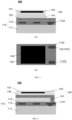
- FIG. 1 is a schematic structural diagram of an optical sensing apparatus provided in an embodiment of the present disclosure.
- FIG. 1(a) is a principal sectional view of the optical sensing apparatus 100
- FIG. 1(b) is a top view of the optical sensing apparatus 100.
- the optical sensing apparatus 100 includes:
- the transparent conductive layer 120 can be configured to be coupled with an electromagnetic wave in an environment, and transmit the electromagnetic wave to the grounding terminal of the sensor chip 110. It should be noted that FIG. 1 does not show the grounding terminal of the sensor chip 110.
- the material of the transparent conductive layer 120 may be at least one of indium tin oxide (ITO), F-doped tin oxide (FTO), and amorphous silicon.
- ITO indium tin oxide
- FTO F-doped tin oxide
- amorphous silicon silicon
- a light transmittance of the transparent conductive layer 120 for the incident light signal is greater than 90%. That is to way, the transparent conductive layer 120 has a high light transmittance, which can reduce the attenuation of the incident light signal.
- the thickness of the transparent conductive layer 120 is 30 nm-50 nm.
- the thickness of the transparent conductive layer 120 is too small, its resistance is large, thereby resulting in poor conductive performance, so that the noise reduction effects are not obvious. Setting the thickness of the transparent conductive layer to 30 nm-50 nm can balance between the light transmittance and conductivity of the transparent conductive layer 120.
- the material of the substrate 111 may be one of silicon substrate, silicon carbide, graphene, indium gallium arsenide, glass, etc.
- the transparent conductive layer 120 when the transparent conductive layer 120 is connected to the grounding terminal 1123 of the wiring layer 112, it only covers or connects the grounding terminal 1123, but does not cover or connect the positive electrode 1124.
- the optical sensing apparatus 100 may further include a first filter structure 130, where the first filter structure 130 is provided above the sensor chip 110, to allow for transmittance of a visible light signal in the incident light signal and filter out an infrared light signal in the incident light signal.
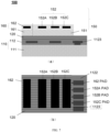
- FIG. 3(a) is a principal sectional view of the optical sensing apparatus 100
- FIG. 3(b) is a top view of the optical sensing apparatus 100.
- the optical sensing apparatus 100 can be applied in scenarios such as ambient light detection and image signal recognition.
- optical detection is performed mainly using the visible light signal in the incident light signal without the need of the infrared light signal. That is to say, in such scenarios, the infrared light signal is an interference signal. Therefore, a first filter structure capable of filtering out the infrared light signal and allowing for transmittance of the visible light signal is provided above the sensor chip, to reduce the interference of the infrared light signal and improve the signal-to-noise ratio.
- the first filter structure 130 may include a first filter layer 131 and a second filter layer 132 stacked from bottom to top.
- the first filter layer 131 can be configured to filter out the infrared light signal in the incident light signal.
- the second filter layer 132 can be configured to allow for transmittance of the visible light signal in the incident light signal.
- the first filter layer 131 may be an IR-cut filter having a function of cutting off infrared light, or may be an antireflective filter film system having a function of cutting off infrared light and antireflecting visible light.
- the second filter layer 132 may be a color filter capable of allowing for transmittance of visible light of a specific color and absorbing visible light in other wavebands, thereby achieving color screening.
- the first filter layer 131 is an inorganic substance
- the second filter layer 132 is an organic substance. Since the materials of the first filter layer 131 and the second filter layer 132 are different, they can be bonded through a transparent organic adhesive layer 101, to improve the reliability.
- the second filter layer 132 may include a plurality of sub-filter layers arranged side by side to allow for transmittance of light signals in a plurality of different wavebands in the visible light signal respectively.
- the second filter layer includes 132A, 132B, and 132C as shown in FIG. 3 .
- the number of sub-filter layers shown in FIG. 3 is only an example, and is not restrictive.
- the 132A, 132B, and 132C may be a red filter, a green filter, and a blue filter respectively, which are configured to allow for transmittance for red light, green light, and blue light respectively.
- the metal wiring layer 1121 of the wiring layer 112 in the sensor chip 110 is not only provided with the grounding terminal 1123, but also provided with a positive electrode corresponding to each sub-filter layer.
- Positive electrodes corresponding to the sub-filter layers 132A, 132B, and 132C are 132A PAD, 132B PAD, and 132C PAD respectively.
- 132A PAD, 132B PAD, and 132C PAD are RED PAD, GREEN PAD, and BLUE PAD respectively.
- the transparent conductive layer 120 may be arranged between the first filter layer 131 and the sensor chip 110. More specifically, the transparent conductive layer 120 is arranged between the first filter layer 131 and the wiring layer 112. As shown in FIG. 3(b) , the transparent conductive layer 120 only covers the grounding terminal 1123 of the metal wiring layer 1121, and does not cover the positive electrodes (132A PAD, 132B PAD, and 132C PAD) of the metal wiring layer 1121, so as to be connected to the grounding terminal 1123.
- the transparent conductive layer 120 only covers the grounding terminal 1123 of the metal wiring layer 1121, and does not cover the positive electrodes (132A PAD, 132B PAD, and 132C PAD) of the metal wiring layer 1121, so as to be connected to the grounding terminal 1123.
- the optical sensing apparatus 100 not only includes the sensor chip 110 and the transparent conductive layer 120, but also may include a second filter structure 140 provided above the sensor chip 110 to allow for transmittance of an infrared light signal in the incident light signal and filter out a visible light signal in the incident light signal.
- the third filter layer 141 may be a Vis-cut filter having a function of blocking or filtering out visible light.
- the fourth filter layer 142 may be an IR-pass color filter capable of allowing for transmittance of infrared light, and absorbing incident light in other wavebands.
- the metal wiring layer 1121 of the wiring layer 112 in the sensor chip 110 is not only provided with the grounding terminal 1123, but also provided with a positive electrode, namely positive electrode 142 PAD, corresponding to the fourth filter layer 142.
- the fourth filter layer 142 is an IR-pass color filter
- the 142 PAD is an IR PAD.
- the transparent conductive layer 120 may also be arranged between the third filter layer 141 and the sensor chip 110. More specifically, the transparent conductive layer 120 is arranged between the third filter layer 141 and the wiring layer 112. As shown in FIG. 5(b) , the transparent conductive layer 120 only covers the grounding terminal 1123 of the metal wiring layer 1121, and does not cover the positive electrode (142 PAD) of the metal wiring layer 1121, so as to be connected to the grounding terminal 1123.
- FIG. 5(b) does not show the third filter layer 141 and the transparent organic adhesive layer 101.
- grounding terminal 1123 in FIG. 5(b) is actually covered by the transparent conductive layer 120, so that the grounding terminal 1123 is annotated with a dotted line and a dotted frame in this figure to distinguish it from the positive electrode (142 PAD) that is not covered by the transparent conductive layer 120.
- the transparent conductive layer 120 may also be arranged between the third filter layer 141 and the fourth filter layer 142.
- the transparent conductive layer 120 is an inorganic substance, and can be bonded with the fourth filter layer 142 through a transparent organic adhesive layer 101, to improve the reliability.
- the transparent conductive layer 120 when the transparent conductive layer 120 is arranged between the third filter layer 141 and the fourth filter layer 142, the transparent conductive layer 120 may be connected to the grounding terminal of the sensor chip 110 along an edge of the third filter layer 141.
- the transparent conductive layer 120 only covers the grounding terminal 1123 of the metal wiring layer 1121, and does not cover the positive electrode of the metal wiring layer 1121, so as to be connected to the grounding terminal 1123.
- FIG. 5(b) may be referred to for the specific connection method.
- the optical sensing apparatus 100 not only includes the sensor chip 110 and the transparent conductive layer 120, but also may include a first filter structure 150 and a second filter structure 160 provided side by side above the sensor chip 110.
- the first filter structure 150 can be configured to allow for transmittance of a visible light signal in the incident light signal and filter out an infrared light signal in the incident light signal.
- the second filter structure 160 can be configured to allow for transmittance of the infrared light signal in the incident light signal and filter out the visible light signal in the incident light signal.
- the optical sensing apparatus 100 can be adapted to a variety of light detection scenarios simultaneously, such as ambient light detection, image signal recognition, and automatic vending, thereby improving the adaptability of the optical sensing apparatus.
- FIG. 7(a) is a principal sectional view of the optical sensing apparatus 100
- FIG. 7(b) is a top view of the optical sensing apparatus 100.
- the first filter structure 150 may include a first filter layer 151 and a second filter layer 152 stacked from bottom to top, where the first filter layer 151 can be configured to filter out the infrared light signal in the incident light signal, and the second filter layer 152 can be configured to allow for transmittance of the visible light signal in the incident light signal.
- the second filter structure 160 may include a third filter layer 161 and a fourth filter layer 162 stacked from bottom to top, where the third filter layer 161 can be configured to filter out the visible light signal in the incident light signal, and the fourth filter layer 162 can be configured to allow for transmittance of the infrared light signal in the incident light signal.
- the first filter structure 150 may be the first filter structure 130 in Embodiment 1.
- the second filter structure 160 may be the second filter structure 140 in Embodiment 2.
- no further details will be given in the present disclosure.
- the transparent conductive layer 120 may be arranged between the sensor chip 110 and the first filter structure 150, and between the sensor chip 110 and the second filter structure 160. As shown in FIG. 7(b) , the transparent conductive layer 120 only covers the grounding terminal 1123 of the metal wiring layer 1121, and does not cover the positive electrodes (152A PAD, 152B PAD, 152C PAD, and 162PAD) of the metal wiring layer 1121, so as to be connected to the grounding terminal 1123.
- the transparent conductive layer 120 only covers the grounding terminal 1123 of the metal wiring layer 1121, and does not cover the positive electrodes (152A PAD, 152B PAD, 152C PAD, and 162PAD) of the metal wiring layer 1121, so as to be connected to the grounding terminal 1123.
- FIG. 7(b) does not show the first filter layer 151 in the above first filter structure 150, the third filter layer 161 in the second filter structure 160, and the transparent organic adhesive layer 101.
- grounding terminal 1123 in FIG. 5(b) is actually covered by the transparent conductive layer 120, so that the grounding terminal 1123 is annotated with a dotted line and a dotted frame in this figure to distinguish it from the positive electrodes (152A PAD, 152B PAD, 152C PAD, and 162PAD) that are not covered by the transparent conductive layer 120.
- the transparent conductive layer 120 may also be arranged between the first filter layer 151 and the second filter layer 152 in the first filter structure 150, and between the third filter layer 161 and the fourth filter layer 162 in the second filter structure 160.
- This arrangement is not shown in the figure, and FIGS. 4 and 6 may be referred to for the specific arrangement positions.
- the transparent conductive layer 120 only covers the grounding terminal 1123 of the metal wiring layer 1121, and does not cover the positive electrode of the metal wiring layer 1121, so as to be connected to the grounding terminal 1123.
- FIG. 7(b) may be referred to for the specific connection method.
- the above first filter structure 150 and the above second filter structure 160 are arranged above the transparent conductive layer 120.
- the first filter structure 150 may include a plurality of first sub-filter structures 151 arranged side by side.
- the plurality of first sub-filter structures 151 are configured to allow for transmittance of light signals in a plurality of different wavebands in the visible light signal respectively, for example, 3 first sub-filter structures 151 as shown in FIG. 8 .
- the number of first sub-filter structures 151 shown in FIG. 8 is only an example and is not restrictive.
- the second filter structure 160 is configured to allow for transmittance of the infrared light signal in the incident light signal and filter out the visible light signal in the incident light signal.
- the plurality of first sub-filter structures 151 in the first filter structure 150 and the second filter structure 160 can be configured to allow for transmittance of light signals in different wavebands respectively.
- FIG. 8(a) is a principal sectional view of the optical sensing apparatus 100
- FIG. 8(b) is a top view of the optical sensing apparatus 100.
- the metal wiring layer 1121 of the wiring layer 112 in the sensor chip 110 is not only provided with the grounding terminal 1123, but also provided with positive electrodes corresponding to the first sub-filter structures 151 and the second filter structure 160 respectively.
- the positive electrode corresponding to the first sub-filter structure 151 is 151 PAD
- the positive electrode corresponding to the second filter structure 160 is 160 PAD.
- the transparent conductive layer 120 only covers the grounding terminal 1123 of the metal wiring layer 1121, and does not cover the positive electrodes (151 PAD and 160 PAD) of the metal wiring layer 1121, so as to be connected to the grounding terminal 1123.
- the transparent conductive layer 120 can be configured to be coupled with an electromagnetic wave in an environment, and transmit the electromagnetic wave to the grounding terminal of the sensor chip 110.
- a transparent conductive layer is manufactured on the sensor chip, and the transparent conductive layer is connected to the grounding terminal of the sensor chip.
- an electromagnetic wave in an environment can be coupled with the transparent conductive layer, and an electromagnetic coupling noise generated therefrom can be eliminated by grounding, and on the other hand, transparency of the transparent conductive layer can allow the optical sensing apparatus to maintain an original incident light amount, thereby improving the signal-to-noise ratio, reducing the operating noise, and improving the optical detection accuracy and user experience.
- the grounding terminal 1123 of the sensor chip 110 may be provided on the substrate 111, and the step S220 may specifically be: manufacturing the transparent conductive layer 120 above the wiring layer 112, where the transparent conductive layer 120 is connected to the grounding terminal of the substrate 111 through a through hole 1125 of the wiring layer 112.
- the wiring layer 112 can be punched by etching to obtain the through hole 1125, where the through hole 1125 runs throughout the whole insulating layer 1122, but does not affect connections between various components or wires of the metal wiring layer 1121. Then, the transparent conductive layer 120 is manufactured in the through hole 1125 and on the wiring layer 112 by coating or spin coating, so that the transparent conductive layer 120 can be connected to the substrate 111, and then connected to the grounding terminal of the substrate 111.
- the first filter structure 130 is configured to allow for transmittance of a visible light signal in the incident light signal and filter out an infrared light signal in the incident light signal.
- the S330 may specifically include the following steps.
- S332 manufacturing a second filter layer 132 above the first filter layer 131.
- the S220 when the S220 is specifically manufacturing the transparent conductive layer 120 on an upper surface of the sensor chip 110, the S331 is specifically forming the first filter layer 131 on an upper surface of the transparent conductive layer 120 by evaporation or sputtering, and the S332 is specifically manufacturing the second filter layer 132 on an upper surface of the first filter layer 131. That is, in the embodiment, the sequence of steps for manufacturing the optical sensing apparatus 100 is: S210, S220, S331, and S332.
- the first filter layer 131 is formed on the upper surface of the transparent conductive layer 120 by evaporation or sputtering, and the first filter layer 131 is manufactured only on the upper surface of the transparent conductive layer 120 except for a region above the positive electrode and the grounding terminal 1123. In other words, the first filter layer 131 does not shield the positive electrode and the grounding terminal 1123, to prevent affecting an electrical connection between the positive electrode and the power source and an electrical connection between the grounding terminal 1123 and the power source.
- the specific manufacturing process of the above S332 may be: coating an organic adhesive layer 101 on the upper surface of the first filter layer 131, then forming the second filter layer 132 on an upper surface of the organic adhesive layer 101 by evaporation or sputtering, and then coating an organic adhesive layer 101 on the second filter layer 132, to seal the second filter layer 132.
- the S331 is specifically manufacturing the first filter layer 131 on the upper surface of the sensor chip 110
- the S220 is specifically manufacturing the transparent conductive layer 120 on the upper surface of the first filter layer 131
- the S332 is specifically manufacturing the second filter layer 132 on the upper surface of the transparent conductive layer 120. That is, the sequence of steps for manufacturing the optical sensing apparatus 100 is: S210, S331, S220, and S332.
- the first filter layer 131 is formed only on the upper surface of the sensor chip 110 except for the region above the positive electrode and the grounding terminal 1123. In other words, the first filter layer 131 does not shield the positive electrode and the grounding terminal 1123, to prevent affecting an electrical connection between the positive electrode and the power source and an electrical connection between the grounding terminal 1123 and the power source.
- the specific manufacturing process of the above S332 may be: coating an organic adhesive layer 101 on the upper surface of the transparent conductive layer 120, then forming the second filter layer 132 on an upper surface of the organic adhesive layer 101 by evaporation or sputtering, and then coating an organic adhesive layer 101 on the second filter layer 132, to seal the second filter layer 132.
- the transparent conductive layer 120 when the transparent conductive layer 120 is manufactured on the upper surface of the first filter layer 131, the transparent conductive layer 120 can also be manufactured on an edge of the first filter layer 131, so that the transparent conductive layer 120 is connected to the grounding terminal of the sensor chip 110 along the edge of the first filter layer 131.
- the S332 may specifically be: manufacturing a plurality of sub-filter layers side by side, where the plurality of sub-filter layers are configured to allow for transmittance of light signals in a plurality of different wavebands in the visible light signal respectively.
- the S332 is specifically manufacturing the plurality of sub-filter layers side by side on the upper surface of the first filter layer 131.
- the S332 is specifically manufacturing the plurality of sub-filter layers side by side on the upper surface of the transparent conductive layer 120.
- FIG. 11 shows a flow block of still another method 400 for manufacturing an optical sensing apparatus.
- the manufacturing method 400 includes S410-S430, where the S410 and the S420 are the same as the S210 and the S220 in the above-mentioned method 200 respectively, and will not be repeated here.
- S430 manufacturing a second filter structure 140 above the sensor chip 110, as shown in FIGS. 5 and 6 .
- the second filter structure 140 is configured to allow for transmittance of the infrared light signal in the incident light signal and filter out the visible light signal in the incident light signal.
- the above S430 may include the following steps.
- the third filter layer 141 is configured to filter out the visible light signal in the incident light signal
- the fourth filter layer 142 is configured to allow for transmittance of the infrared light signal in the incident light signal.
- the S220 is specifically manufacturing the transparent conductive layer 120 on an upper surface of the sensor chip 110
- the S431 is specifically forming the third filter layer 141 on an upper surface of the transparent conductive layer 120 by evaporation or sputtering
- the S432 is specifically manufacturing the fourth filter layer 142 on an upper surface of the third filter layer 141. That is, the sequence of steps for manufacturing the optical sensing apparatus 100 is: S210, S220, S431, and S432.
- the third filter layer 141 when the S431 is forming the third filter layer 141 on the upper surface of the transparent conductive layer 120 by evaporation or sputtering, the third filter layer 141 is manufactured only on the upper surface of the transparent conductive layer 120 except for a region above the positive electrode and the grounding terminal 1123. In other words, the third filter layer 141 does not shield the positive electrode and the grounding terminal 1123, to prevent affecting an electrical connection between the positive electrode and the power source and an electrical connection between the grounding terminal 1123 and the power source.
- the specific manufacturing process of the S432 may be: coating an organic adhesive layer 101 on the upper surface of the third filter layer 141, then forming the fourth filter layer 142 on an upper surface of the organic adhesive layer 101 by evaporation or sputtering, and then coating an organic adhesive layer 101 on the fourth filter layer 142, to seal the fourth filter layer 142.
- the S431 is specifically manufacturing the third filter layer 141 on the upper surface of the sensor chip 110
- the S220 is specifically manufacturing the transparent conductive layer 120 on the upper surface of the third filter layer 141
- the S432 is specifically manufacturing the fourth filter layer 142 on the upper surface of the transparent conductive layer 120. That is, the sequence of steps for manufacturing the optical sensing apparatus 100 is: S210, S431, S220, and S432.
- the third filter layer 141 is formed only on the upper surface of the sensor chip 110 except for the region above the positive electrode and the grounding terminal 1123.
- the first filter layer 131 does not shield the positive electrode and the grounding terminal 1123, to prevent affecting an electrical connection between the positive electrode and the power source and an electrical connection between the grounding terminal 1123 and the power source.
- the specific manufacturing process of the S432 may be: coating an organic adhesive layer 101 on the upper surface of the transparent conductive layer 120, then forming the fourth filter layer 142 on an upper surface of the organic adhesive layer 101 by evaporation or sputtering, and then coating an organic adhesive layer 101 on the fourth filter layer 142, to seal the fourth filter layer 142.
- the transparent conductive layer 120 when the transparent conductive layer 120 is manufactured on the upper surface of the third filter layer 141, the transparent conductive layer 120 can also be manufactured on an edge of the third filter layer 141, so that the transparent conductive layer 120 is connected to the grounding terminal of the sensor chip 110 along the edge of the first filter layer 141.
- FIG. 12 shows a flow block of yet another method 500 for manufacturing an optical sensing apparatus.
- the manufacturing method 500 includes S510-S530, where the S510 and the S520 are the same as the S210 and the S220 in the above-mentioned method 200 respectively, and will not be repeated here.
- the first filter structure 150 is configured to allow for transmittance of a visible light signal in the incident light signal and filter out an infrared light signal in the incident light signal.
- the second filter structure 160 is configured to allow for transmittance of the infrared light signal in the incident light signal and filter out the visible light signal in the incident light signal.
- the above-mentioned S530 may include the following steps.
- S532 manufacturing a second filter layer 152 above the first filter layer 151, and manufacturing a fourth filter layer 162 above the third filter layer 161, where the second filter layer 152 and the fourth filter layer 152 are arranged side by side.
- the first filter layer 151 is configured to filter out the infrared light signal in the incident light signal
- the second filter layer 152 is configured to allow for transmittance of the visible light signal in the incident light signal
- the third filter layer 161 is configured to filter out the visible light signal in the incident light signal
- the fourth filter layer 162 is configured to allow for transmittance of the infrared light signal in the incident light signal.
- the first filter layer 151 and the third filter layer 161 are formed on the upper surface of the transparent conductive layer 120 by evaporation or sputtering, and the first filter layer 151 and the third filter layer 161 are manufactured only on the upper surface of the transparent conductive layer 120 except for a region above the positive electrode and the grounding terminal 1123.
- the first filter layer 151 and the third filter layer 161 do not shield the positive electrode and the grounding terminal 1123, to prevent affecting an electrical connection between the positive electrode and the power source and an electrical connection between the grounding terminal 1123 and the power source.
Landscapes
- Engineering & Computer Science (AREA)
- Physics & Mathematics (AREA)
- General Physics & Mathematics (AREA)
- Human Computer Interaction (AREA)
- Multimedia (AREA)
- Theoretical Computer Science (AREA)
- Optics & Photonics (AREA)
- Light Receiving Elements (AREA)
- Photometry And Measurement Of Optical Pulse Characteristics (AREA)
- Measurement Of The Respiration, Hearing Ability, Form, And Blood Characteristics Of Living Organisms (AREA)
Abstract
Description
- The present disclosure claims priority to the patent application for invention with the application number
202310490886.1 titled "OPTICAL SENSING APPARATUS, METHOD FOR MANUFACTURING OPTICAL SENSING APPARATUS, AND ELECTRONIC DEVICE" filed with the China National Intellectual Property Administration on 28 April 2023 - The present disclosure relates to the technical field of optical sensing, and more specifically relates to an optical sensing apparatus, a method for manufacturing an optical sensing apparatus, and an electronic device.
- At present, with the development of optical sensing apparatuses, they are increasingly widely used in electronic products, such as ambient light detection, image signal recognition, and under-display fingerprint recognition.
- However, an electromagnetic wave in an environment tends to have electromagnetic induction with a metal circuit in an optical sensing apparatus, thereby generating an electromagnetic noise. This will not only cause a high operating noise of electronic products and affect the user experience, but also reduce the signal-to-noise ratio and affect the optical detection accuracy.
- Embodiments of the present disclosure provide a near field communication apparatus and an electronic device, which can improve the performance of near field communication.
- An embodiment of the present disclosure provides an optical sensing apparatus, a method for manufacturing an optical sensing apparatus, and an electronic device, which can improve the optical detection accuracy and user experience.
- In a first aspect, an optical sensing apparatus is provided, including: a sensor chip configured to receive an incident light signal for optical detection; and a transparent conductive layer provided above the sensor chip and connected to a grounding terminal of the sensor chip.
- In technical solutions of the embodiment of the present disclosure, the transparent conductive layer is provided on the sensor chip, and the transparent conductive layer is connected to the grounding terminal of the sensor chip. In this way, on the one hand, an electromagnetic wave in an environment can be coupled with the transparent conductive layer above the sensor chip, and an electromagnetic coupling noise generated therefrom can be eliminated by grounding, and on the other hand, transparency of the transparent conductive layer can allow the optical sensing apparatus to maintain an original incident light amount, thereby improving the signal-to-noise ratio, reducing the operating noise, and improving the optical detection accuracy and user experience.
- In a possible embodiment, the sensor chip includes a substrate and a wiring layer provided on an upper surface of the substrate; the grounding terminal of the sensor chip is arranged at the wiring layer, and the transparent conductive layer is arranged above the wiring layer and connected to the grounding terminal.
- In a possible embodiment, the sensor chip includes a substrate and a wiring layer provided on an upper surface of the substrate; the grounding terminal of the sensor chip is arranged at the substrate, and the transparent conductive layer is arranged above the wiring layer and runs through a through hole of the wiring layer for connection to the grounding terminal.
- In a possible embodiment, the optical sensing apparatus further includes a first filter structure provided above the sensor chip to allow for transmittance of a visible light signal in the incident light signal and filter out an infrared light signal in the incident light signal.
- When the optical sensing apparatus is applied in a scenario such as ambient light detection and image signal recognition, the first filter structure capable of filtering out the infrared light signal and allowing for transmittance of the visible light signal is arranged to reduce the interference of the infrared light signal and improve the signal-to-noise ratio.
- In a possible embodiment, the first filter structure includes a first filter layer and a second filter layer stacked from bottom to top; where the first filter layer is configured to filter out the infrared light signal in the incident light signal; and the second filter layer is configured to allow for transmittance of the visible light signal in the incident light signal.
- In a possible embodiment, the second filter layer includes a plurality of sub-filter layers arranged side by side to allow for transmittance of light signals in a plurality of different wavebands in the visible light signal respectively.
- In a possible embodiment, when the transparent conductive layer is arranged between the first filter layer and the second filter layer; or the transparent conductive layer is arranged between the first filter layer and the sensor chip.
- In a possible embodiment, when the transparent conductive layer is arranged between the first filter layer and the second filter layer, the transparent conductive layer is connected to the grounding terminal of the sensor chip along an edge of the first filter layer.
- In a possible embodiment, the optical sensing apparatus further includes a second filter structure provided above the sensor chip to allow for transmittance of an infrared light signal in the incident light signal and filter out a visible light signal in the incident light signal.
- When the optical sensing apparatus is applied in a scenario of automatic vending, the second filter structure capable of allowing for transmittance of the infrared light signal and filtering out the visible light signal is arranged to reduce the interference of the visible light signal and improve the signal-to-noise ratio.
- In a possible embodiment, the second filter structure includes a third filter layer and a fourth filter layer stacked from bottom to top; where the third filter layer is configured to filter out the visible light signal in the incident light signal; and the fourth filter layer is configured to allow for transmittance of the infrared light signal in the incident light signal.
- In a possible embodiment, when the transparent conductive layer is arranged between the third filter layer and the fourth filter layer; or the transparent conductive layer is arranged between the third filter layer and the sensor chip.
- In a possible embodiment, when the transparent conductive layer is arranged between the third filter layer and the fourth filter layer, the transparent conductive layer is connected to the grounding terminal of the sensor chip along an edge of the third filter layer.
- In a possible embodiment, the optical sensing apparatus further includes a first filter structure and a second filter structure arranged side by side above the sensor chip; where the first filter structure is configured to allow for transmittance of the visible light signal in the incident light signal and filter out the infrared light signal in the incident light signal; and the second filter structure is configured to allow for transmittance of the infrared light signal in the incident light signal and filter out the visible light signal in the incident light signal.
- Not only is the first filter structure capable of filtering out the infrared light signal and allowing for transmittance of the visible light signal arranged above the sensor chip, but also the second filter structure capable of allowing for transmittance of the infrared light signal and filtering out the visible light signal is arranged, so as to be adapted to a variety of optical detection scenarios, such as ambient light detection, image signal recognition, and automatic vending, thereby improving the adaptability of the optical sensing apparatus.
- In a possible embodiment, the first filter structure and the second filter structure are arranged above the transparent conductive layer; and the first filter structure includes a plurality of first sub-filter structures arranged side by side to allow for transmittance of light signals in a plurality of different wavebands in the visible light signal respectively.
- In the embodiment, not only can the optical sensing apparatus be adapted to a variety of optical detection scenarios, but also the overall thickness of the optical sensing apparatus can be reduced, which is beneficial to achieving a thin and light electronic device equipped with the optical sensing apparatus.
- In a possible embodiment, a material of the transparent conductive layer is at least one of indium tin oxide, F-doped, and amorphous silicon.
- In a possible embodiment, a light transmittance of the transparent conductive layer for the incident light signal is greater than 90%. The transparent
conductive layer 120 has a high light transmittance, which can reduce the attenuation of the incident light signal. - In a possible embodiment, a thickness of the transparent conductive layer is less than or equal to 100 nm. Controlling the thickness of the transparent conductive layer to be within 100 nm can ensure the light transmittance and the incident light amount of the transparent conductive layer.
- In a possible embodiment, a thickness of the transparent conductive layer is 30 nm-50 nm. Setting the thickness of the transparent conductive layer to 30 nm-50 nm can balance between the light transmittance and conductivity of the transparent conductive layer.
- In a possible embodiment, an impedance of the transparent conductive layer is less than or equal to 30 Ω/cm2. When the impedance of the transparent conductive layer is less than or equal to 30 Ω/cm2, it can ensure that the transparent conductive layer has a minimum conductive performance required to conduct the electromagnetic coupling noise to the grounding terminal.
- In a possible embodiment, the transparent conductive layer is formed on the sensor chip by coating or spin coating.
- In a possible embodiment, the optical sensing apparatus is used in an electronic device with a display screen and is configured to be arranged below the display screen, and the sensor chip is configured to receive the incident light signal through the display screen for under-display optical detection.
- In a second aspect, a method for manufacturing an optical sensing apparatus is provided, including: providing a sensor chip configured to receive an incident light signal for optical detection; and manufacturing a transparent conductive layer above the sensor chip, where the transparent conductive layer is connected to a grounding terminal of the sensor chip.
- In technical solutions of the embodiment of the present disclosure, the transparent conductive layer is manufactured on the sensor chip, and the transparent conductive layer is connected to the grounding terminal of the sensor chip. In this way, on the one hand, an electromagnetic wave in an environment can be coupled with the transparent conductive layer above the sensor chip, and an electromagnetic coupling noise generated therefrom can be eliminated by grounding, and on the other hand, transparency of the transparent conductive layer can allow the optical sensing apparatus to maintain an original incident light amount, thereby improving the signal-to-noise ratio, reducing the operating noise, and improving the optical detection accuracy and user experience.
- In a possible embodiment, the sensor chip includes a substrate and a wiring layer provided on an upper surface of the substrate, and the grounding terminal of the sensor is provided at the wiring layer; and the manufacturing the transparent conductive layer above the sensor chip includes: manufacturing the transparent conductive layer above the wiring layer, where the transparent conductive layer is connected to the grounding terminal at the wiring layer.
- In a possible embodiment, the sensor chip includes a substrate and a wiring layer provided on an upper surface of the substrate, the grounding terminal of the sensor chip is arranged at the substrate; and the manufacturing the transparent conductive layer above the sensor chip includes: manufacturing the transparent conductive layer above the wiring layer, where the transparent conductive layer is connected to the grounding terminal of the substrate through a through hole of the wiring layer.
- In a possible embodiment, the manufacturing method further includes: manufacturing a first filter structure above the sensor chip, where the first filter structure is configured to allow for transmittance of a visible light signal in the incident light signal and filter out an infrared light signal in the incident light signal.
- In a possible embodiment, the manufacturing the first filter structure above the sensor chip includes: manufacturing a first filter layer; and manufacturing a second filter layer above the first filter layer; where the first filter layer is configured to filter out the infrared light signal in the incident light signal, and the second filter layer is configured to allow for transmittance of the visible light signal in the incident light signal.
- In a possible embodiment, the manufacturing the second filter layer above the first filter layer includes: manufacturing a plurality of sub-filter layers side by side, where the plurality of sub-filter layers are configured to allow for transmittance of light signals in a plurality of different wavebands in the visible light signal respectively.
- In a possible embodiment, the manufacturing the transparent conductive layer above the sensor chip includes: manufacturing the transparent conductive layer on an upper surface of the sensor chip prior to the manufacturing the first filter layer; or manufacturing the transparent conductive layer on an upper surface of the first filter layer after the manufacturing the first filter layer.
- In a possible embodiment, the manufacturing the transparent conductive layer above the sensor chip further includes: manufacturing the transparent conductive layer on an edge of the first filter layer, where the transparent conductive layer is connected to the grounding terminal of the sensor chip along the edge of the first filter layer.
- In a possible embodiment, the manufacturing method further includes: manufacturing a second filter structure above the sensor chip, where the second filter structure is configured to allow for transmittance of an infrared light signal in the incident light signal and filter out a visible light signal in the incident light signal.
- In a possible embodiment, the manufacturing the second filter structure above the sensor chip includes: manufacturing a third filter layer; and manufacturing a fourth filter layer above the third filter layer; where the third filter layer is configured to filter out the visible light signal in the incident light signal, and the fourth filter layer is configured to allow for transmittance of the infrared light signal in the incident light signal.
- In a possible embodiment, the manufacturing the transparent conductive layer above the sensor chip includes: manufacturing the transparent conductive layer on an upper surface of the sensor chip prior to the manufacturing the third filter layer; or manufacturing the transparent conductive layer on an upper surface of the third filter layer after the manufacturing the third filter layer.
- In a possible embodiment, the manufacturing the transparent conductive layer above the sensor chip further includes: manufacturing the transparent conductive layer on an edge of the third filter layer, where the transparent conductive layer is connected to the grounding terminal of the sensor chip along the edge of the third filter layer.
- In a possible embodiment, the manufacturing method further includes: manufacturing a first filter structure and a second filter structure side by side above the sensor chip; where the first filter structure is configured to allow for transmittance of the visible light signal in the incident light signal and filter out the infrared light signal in the incident light signal; and the second filter structure is configured to allow for transmittance of the infrared light signal in the incident light signal and filter out the visible light signal in the incident light signal.
- In a possible embodiment, the manufacturing the first filter structure and the second filter structure side by side above the sensor chip includes: manufacturing the first filter structure and the second filter structure above the transparent conductive layer; and the manufacturing the first filter structure above the transparent conductive layer includes: manufacturing a plurality of first sub-filter structures side by side, where the plurality of first sub-filter structures are configured to allow for transmittance of light signals in a plurality of different wavebands in the visible light signal respectively.
- In a possible embodiment, the transparent conductive layer is manufactured on the sensor chip by coating or spin coating.
- In a third aspect, an electronic device is provided, including: the optical sensing apparatus according to the first aspect or any one possible embodiment of the first aspect, or the optical sensing apparatus manufactured according to the second aspect or any one possible embodiment of the second aspect.
-
-
FIG. 1 is a schematic structural diagram of an optical sensing apparatus according to an embodiment of the present disclosure. -
FIG. 2 is a schematic structural diagram of another optical sensing apparatus according to an embodiment of the present disclosure. -
FIGS. 3 to 8 are schematic structural diagrams of several other apparatuses for recognizing an optical fingerprint according to embodiments of the present disclosure. -
FIG. 9 is a flow block of a method for manufacturing an optical sensing apparatus according to an embodiment of the present disclosure. -
FIGS. 10 to 12 are flow blocks of several other methods for manufacturing an optical sensing apparatus according to embodiments of the present disclosure. - Technical solutions of embodiments of the present disclosure will be described below with reference to the drawings.
- An optical sensing apparatus in an embodiment of the present disclosure can be applied to various electronic devices, and are particularly adapted to computers and peripherals thereof, communications, consumer-electronics, and other 3C electronic products, for example, smart phones, notebook computers, tablet computers, smart wearable devices, household appliances, game devices, etc. In addition, the optical sensing apparatus can be further applied to other types of electronic devices such as automotive electronics.
- As an example and non-restrictively, the optical sensing apparatus in the embodiment of the present disclosure can be used in a light signal detection system, for example, ambient light detection, which can automatically adjust keyboard light, screen brightness, etc., and for another example, infrared light detection, which can achieve automatic vending, etc. The optical sensing apparatus in the embodiment of the present disclosure can also be used in an optical imaging system, such as image signal recognition, and can still be used in an optical recognition system, such as optical fingerprint recognition.
- In the optical imaging system, a conventional optical sensing apparatus can partially filter out the infrared light in the incident light signal by providing an infrared filter or a color filter, thereby obtaining a light signal and an image close to responses of human eyes. However, this method can only filter out non-visible light signals in a signal source, but cannot shield electromagnetic interference. Specifically, an electromagnetic wave in an environment tends to have electromagnetic induction with a metal circuit in the optical sensing apparatus, thereby resulting in a high noise of an electronic device, affecting the user experience, reducing the signal-to-noise ratio of the signal, and affecting the optical detection accuracy.
- At present, in order to reduce the impact of electromagnetic interference on the noise and the signal-to-noise ratio, one solution is to place a grounded metal grid layer on a sensor chip of the optical sensing apparatus to guide an electromagnetic wave signal to a grounding terminal through metal shielding, but this method will reduce the light transmittance area of the sensor chip and reduce an amount of incident light received by the sensor chip. In other words, this method reduces the noise, but will also reduce the signal amount, thereby unobviously improving the signal-to-noise ratio, or even reducing the signal-to-noise ratio. Another solution is to achieve electromagnetic shielding by providing a transparent conductive substrate outside a screen of the electronic device. This method consumes less incident light, but is not compatible with a wafer process, and is very difficult to interconnect with a grounding terminal of the sensor chip, thereby failing to guide away the electromagnetic wave signal with unobvious noise reduction effects.
- In view of this, an embodiment of the present disclosure provides an optical sensing apparatus that can reduce the impact of the electromagnetic wave in the environment on the noise and signal-to-noise ratio, and improve the optical detection accuracy and user experience.
-
FIG. 1 is a schematic structural diagram of an optical sensing apparatus provided in an embodiment of the present disclosure.FIG. 1(a) is a principal sectional view of theoptical sensing apparatus 100, andFIG. 1(b) is a top view of theoptical sensing apparatus 100. As shown inFIG. 1 , theoptical sensing apparatus 100 includes: - a
sensor chip 110 configured to receive an incident light signal for optical detection; and - a transparent
conductive layer 120 provided above thesensor chip 110 and connected to a grounding terminal of thesensor chip 110. - The transparent
conductive layer 120 can be configured to be coupled with an electromagnetic wave in an environment, and transmit the electromagnetic wave to the grounding terminal of thesensor chip 110. It should be noted thatFIG. 1 does not show the grounding terminal of thesensor chip 110. - Therefore, in the optical sensing apparatus in the embodiment of the present disclosure, the transparent conductive layer can be provided on the sensor chip, and the transparent conductive layer is connected to the grounding terminal of the sensor chip. In this way, on the one hand, the electromagnetic wave in the environment can be coupled with the transparent conductive layer, and an electromagnetic coupling noise generated therefrom can be eliminated by grounding, and on the other hand, transparency of the transparent conductive layer can allow the optical sensing apparatus to maintain an original incident light amount, thereby improving the signal-to-noise ratio, reducing the operating noise, and improving the optical detection accuracy and user experience.
- Optionally, the material of the transparent
conductive layer 120 may be at least one of indium tin oxide (ITO), F-doped tin oxide (FTO), and amorphous silicon. - Optionally, a light transmittance of the transparent
conductive layer 120 for the incident light signal is greater than 90%. That is to way, the transparentconductive layer 120 has a high light transmittance, which can reduce the attenuation of the incident light signal. - Optionally, a thickness of the transparent
conductive layer 120 is less than or equal to 100 nm. When the thickness of the transparentconductive layer 120 is larger than 100 nm, that is, when the thickness of the transparentconductive layer 120 is too large, the light transmittance of the transparentconductive layer 120 will be reduced, thereby increasing the attenuation of the incident light signal. Therefore, controlling the thickness of the transparent conductive layer to be within 100 nm can ensure the light transmittance and incident light amount of the transparentconductive layer 120. - Optionally, the thickness of the transparent
conductive layer 120 is 30 nm-50 nm. When the thickness of the transparentconductive layer 120 is too small, its resistance is large, thereby resulting in poor conductive performance, so that the noise reduction effects are not obvious. Setting the thickness of the transparent conductive layer to 30 nm-50 nm can balance between the light transmittance and conductivity of the transparentconductive layer 120. - Optionally, an impedance of the transparent
conductive layer 120 is less than or equal to 30 Ω/cm2. It should be understood that when the impedance of the transparentconductive layer 120 is too large, its conductive performance is poor, so that the noise reduction effects are not obvious. When the impedance of the transparentconductive layer 120 is less than or equal to 30 Ω/cm2, it can ensure that the transparentconductive layer 120 has a minimum conductive performance required to conduct the electromagnetic coupling noise to the grounding terminal. - Further referring to
FIG. 1(a) , thesensor chip 110 in the embodiment of the present disclosure may include asubstrate 111 and awiring layer 112 provided on an upper surface of thesubstrate 111. Thewiring layer 112 may include ametal wiring layer 1121 and an insulatinglayer 1122, and themetal wiring layer 1121 may be cladded by the insulatinglayer 1122. - In the embodiment of the present disclosure, the material of the
substrate 111 may be one of silicon substrate, silicon carbide, graphene, indium gallium arsenide, glass, etc. - Optionally, in some embodiments, further referring to
FIG. 1 , the transparentconductive layer 120 may be provided above thewiring layer 112, and may be connected to agrounding terminal 1123 of thewiring layer 112. - As shown in
FIG. 1(b) , themetal wiring layer 1121 of thewiring layer 112 not only includes a metal circuit, but also includes agrounding terminal 1123 and apositive electrode 1124. Thegrounding terminal 1123 may also be referred to as a grounding pad, a negative electrode, a GND PAD, etc. Thepositive electrode 1124 may also be referred to as a positive electrode pad, a PAD, etc. Generally, thegrounding terminal 1123 and thepositive electrode 1124 are not covered or shielded by the insulatinglayer 1122, so that thegrounding terminal 1123 and thepositive electrode 1124 are electrically connected to a power source or other components. - It should be noted that when the transparent
conductive layer 120 is connected to thegrounding terminal 1123 of thewiring layer 112, it only covers or connects thegrounding terminal 1123, but does not cover or connect thepositive electrode 1124. - It should be further noted that the
grounding terminal 1123 inFIG. 1(b) is actually covered by the transparentconductive layer 120, so that thegrounding terminal 1123 is annotated with a dotted line and a dotted frame in this figure to distinguish it from thepositive electrode 1124 that is not covered by the transparentconductive layer 120. - Optionally, in some embodiments, as shown in
FIG. 2 , the transparentconductive layer 120 may be provided above thewiring layer 112, and thewiring layer 112 has a throughhole 1125, so that the transparentconductive layer 120 can be connected to the grounding terminal of thesubstrate 111 through the throughhole 1125. - It should be noted that the grounding terminal of the
substrate 111 is not shown inFIG. 2 . Since thesubstrate 111 itself is grounded, when the transparentconductive layer 120 is connected to thesubstrate 111 through the throughhole 1125, it is equivalent to being connected to the grounding terminal of thesubstrate 111. - It should be further noted that the through
hole 1122 on thewiring layer 112 can run throughout thewhole wiring layer 112, but will not affect connections between various components or wires of themetal wiring layer 1121. - It should be understood that by the above-mentioned manufacturing the transparent
conductive layer 120 above thesensor chip 110, the impact of the electromagnetic wave in the environment on the signal-to-noise ratio can be reduced. Further, in different application scenarios, different filter structures can also be used to reduce the impact of interfering light signals on the signal-to-noise ratio. - Optionally, as an embodiment, denoted as Embodiment 1, as shown in
FIG. 3 , theoptical sensing apparatus 100 may further include afirst filter structure 130, where thefirst filter structure 130 is provided above thesensor chip 110, to allow for transmittance of a visible light signal in the incident light signal and filter out an infrared light signal in the incident light signal. -
FIG. 3(a) is a principal sectional view of theoptical sensing apparatus 100, andFIG. 3(b) is a top view of theoptical sensing apparatus 100. - As an example and non-restrictively, the
optical sensing apparatus 100 can be applied in scenarios such as ambient light detection and image signal recognition. In such scenarios, optical detection is performed mainly using the visible light signal in the incident light signal without the need of the infrared light signal. That is to say, in such scenarios, the infrared light signal is an interference signal. Therefore, a first filter structure capable of filtering out the infrared light signal and allowing for transmittance of the visible light signal is provided above the sensor chip, to reduce the interference of the infrared light signal and improve the signal-to-noise ratio. - Embodiment 1 is described below by taking the transparent
conductive layer 120 connected to thegrounding terminal 1123 of thewiring layer 112 in thesensor chip 110 as an example. Of course, the transparentconductive layer 120 may also be connected to the grounding terminal of thesubstrate 111 in thesensor chip 110, but this connection method is not shown in the figure. - Optionally, in some embodiments, further referring to
FIG. 3 , thefirst filter structure 130 may include afirst filter layer 131 and asecond filter layer 132 stacked from bottom to top. Thefirst filter layer 131 can be configured to filter out the infrared light signal in the incident light signal. Thesecond filter layer 132 can be configured to allow for transmittance of the visible light signal in the incident light signal. - Specifically, the
first filter layer 131 may be an IR-cut filter having a function of cutting off infrared light, or may be an antireflective filter film system having a function of cutting off infrared light and antireflecting visible light. Thesecond filter layer 132 may be a color filter capable of allowing for transmittance of visible light of a specific color and absorbing visible light in other wavebands, thereby achieving color screening. - Generally, the
first filter layer 131 is an inorganic substance, and thesecond filter layer 132 is an organic substance. Since the materials of thefirst filter layer 131 and thesecond filter layer 132 are different, they can be bonded through a transparent organicadhesive layer 101, to improve the reliability. - Optionally, in some embodiments, the
second filter layer 132 may include a plurality of sub-filter layers arranged side by side to allow for transmittance of light signals in a plurality of different wavebands in the visible light signal respectively. For example, the second filter layer includes 132A, 132B, and 132C as shown inFIG. 3 . The number of sub-filter layers shown inFIG. 3 is only an example, and is not restrictive. - As an example and non-restrictively, the 132A, 132B, and 132C may be a red filter, a green filter, and a blue filter respectively, which are configured to allow for transmittance for red light, green light, and blue light respectively.
- As shown in
FIG. 3(b) , themetal wiring layer 1121 of thewiring layer 112 in thesensor chip 110 is not only provided with thegrounding terminal 1123, but also provided with a positive electrode corresponding to each sub-filter layer. Positive electrodes corresponding to thesub-filter layers - For example, when the
sub-filter layers - Optionally, in some embodiments, further referring to
FIG. 3 , the transparentconductive layer 120 may be arranged between thefirst filter layer 131 and thesensor chip 110. More specifically, the transparentconductive layer 120 is arranged between thefirst filter layer 131 and thewiring layer 112. As shown inFIG. 3(b) , the transparentconductive layer 120 only covers thegrounding terminal 1123 of themetal wiring layer 1121, and does not cover the positive electrodes (132A PAD, 132B PAD, and 132C PAD) of themetal wiring layer 1121, so as to be connected to thegrounding terminal 1123. - It should be noted that, in order to clearly show a connection relationship between the transparent
conductive layer 120 and themetal wiring layer 1121,FIG. 3(b) does not show thefirst filter layer 131 and the transparent organicadhesive layer 101. - It should be further noted that the
grounding terminal 1123 inFIG. 3(b) is actually covered by the transparentconductive layer 120, so that thegrounding terminal 1123 is annotated with a dotted line and a dotted frame in this figure to distinguish it from the positive electrodes (132A PAD, 132B PAD, and 132C PAD) that are not covered by the transparentconductive layer 120. - Optionally, in some embodiments, as shown in
FIG. 4 , the transparentconductive layer 120 may also be arranged between thefirst filter layer 131 and thesecond filter layer 132. The transparentconductive layer 120 is an inorganic substance, and the transparentconductive layer 120 and thesecond filter layer 132 can be bonded through a transparent organicadhesive layer 101, to improve the reliability. In the embodiment, the transparentconductive layer 120 only covers thegrounding terminal 1123 of themetal wiring layer 1121, and does not cover the positive electrode of themetal wiring layer 1121, so as to be connected to thegrounding terminal 1123.FIG. 3(b) may be referred to for the specific connection method. - Specifically, when the transparent
conductive layer 120 is arranged between thefirst filter layer 131 and thesecond filter layer 132, further referring toFIG. 4 , the transparentconductive layer 120 may be connected to thegrounding terminal 1123 of thesensor chip 110 along an edge of thefirst filter layer 131. - It should be understood that the positive electrode and the
grounding terminal 1123 of themetal wiring layer 1121 in thesensor chip 110 are generally arranged at an edge position to facilitate connection with the power source. When the transparentconductive layer 120 is arranged between thefirst filter layer 131 and thesecond filter layer 132, the transparentconductive layer 120 is connected to thegrounding terminal 1123 along the edge of thefirst filter layer 131 to reduce the process difficulty. - Optionally, as another embodiment, denoted as
Embodiment 2, as shown inFIG. 5 , theoptical sensing apparatus 100 not only includes thesensor chip 110 and the transparentconductive layer 120, but also may include asecond filter structure 140 provided above thesensor chip 110 to allow for transmittance of an infrared light signal in the incident light signal and filter out a visible light signal in the incident light signal. - As an example and non-restrictively, the
optical sensing apparatus 100 can be applied in scenarios of automatic vending, such as automatic vending of water. In such scenarios, optical detection is performed mainly using the infrared light signal in the incident light signal. The infrared light signal may be transmitted from an infrared light source, and the visible light signal in the environment may interfere with the infrared light signal. Therefore, the second filter structure capable of allowing for transmittance of the infrared light signal and filtering out the visible light signal is provided above the sensor chip to reduce the interference with the visible light signal, and improve the signal-to-noise ratio. -
Embodiment 2 is described below by taking the transparentconductive layer 120 connected to thegrounding terminal 1123 of themetal wiring layer 1121 in thesensor chip 110 as an example, and of course, the transparentconductive layer 120 may also be connected to the grounding terminal of thesubstrate 111 in thesensor chip 110, which is not limited in the present disclosure. - Optionally, in some embodiments, as shown in
FIG. 5 , thesecond filter structure 140 may include athird filter layer 141 and afourth filter layer 142 stacked from bottom to top. Thethird filter layer 141 can be configured to filter out the visible light signal in the incident light signal. Thefourth filter layer 142 can be configured to allow for transmittance of the infrared light signal in the incident light signal. -
FIG. 5(a) is a principal sectional view of theoptical sensing apparatus 100, andFIG. 5(b) is a top view of theoptical sensing apparatus 100. - Specifically, the
third filter layer 141 may be a Vis-cut filter having a function of blocking or filtering out visible light. Thefourth filter layer 142 may be an IR-pass color filter capable of allowing for transmittance of infrared light, and absorbing incident light in other wavebands. - Generally, the
third filter layer 141 is an inorganic substance, and thefourth filter layer 142 is an organic substance. Since the materials of thethird filter layer 141 and thefourth filter layer 142 are different, they can be bonded through a transparent organicadhesive layer 101, to improve the reliability. - As shown in
FIG. 5(b) , themetal wiring layer 1121 of thewiring layer 112 in thesensor chip 110 is not only provided with thegrounding terminal 1123, but also provided with a positive electrode, namelypositive electrode 142 PAD, corresponding to thefourth filter layer 142. When thefourth filter layer 142 is an IR-pass color filter, the 142 PAD is an IR PAD. - Optionally, in some embodiments, further referring to
FIG. 5 , the transparentconductive layer 120 may also be arranged between thethird filter layer 141 and thesensor chip 110. More specifically, the transparentconductive layer 120 is arranged between thethird filter layer 141 and thewiring layer 112. As shown inFIG. 5(b) , the transparentconductive layer 120 only covers thegrounding terminal 1123 of themetal wiring layer 1121, and does not cover the positive electrode (142 PAD) of themetal wiring layer 1121, so as to be connected to thegrounding terminal 1123. - It should be noted that, in order to clearly show the connection relationship between the transparent
conductive layer 120 and themetal wiring layer 1121,FIG. 5(b) does not show thethird filter layer 141 and the transparent organicadhesive layer 101. - It should be further noted that the
grounding terminal 1123 inFIG. 5(b) is actually covered by the transparentconductive layer 120, so that thegrounding terminal 1123 is annotated with a dotted line and a dotted frame in this figure to distinguish it from the positive electrode (142 PAD) that is not covered by the transparentconductive layer 120. - Optionally, in some embodiments, as shown in
FIG. 6 , the transparentconductive layer 120 may also be arranged between thethird filter layer 141 and thefourth filter layer 142. The transparentconductive layer 120 is an inorganic substance, and can be bonded with thefourth filter layer 142 through a transparent organicadhesive layer 101, to improve the reliability. - Specifically, further referring to
FIG. 6 , when the transparentconductive layer 120 is arranged between thethird filter layer 141 and thefourth filter layer 142, the transparentconductive layer 120 may be connected to the grounding terminal of thesensor chip 110 along an edge of thethird filter layer 141. In the embodiment, the transparentconductive layer 120 only covers thegrounding terminal 1123 of themetal wiring layer 1121, and does not cover the positive electrode of themetal wiring layer 1121, so as to be connected to thegrounding terminal 1123.FIG. 5(b) may be referred to for the specific connection method. - Optionally, as another embodiment, denoted as
Embodiment 3, as shown inFIG. 7 , theoptical sensing apparatus 100 not only includes thesensor chip 110 and the transparentconductive layer 120, but also may include afirst filter structure 150 and asecond filter structure 160 provided side by side above thesensor chip 110. Thefirst filter structure 150 can be configured to allow for transmittance of a visible light signal in the incident light signal and filter out an infrared light signal in the incident light signal. Thesecond filter structure 160 can be configured to allow for transmittance of the infrared light signal in the incident light signal and filter out the visible light signal in the incident light signal. In this way, theoptical sensing apparatus 100 can be adapted to a variety of light detection scenarios simultaneously, such as ambient light detection, image signal recognition, and automatic vending, thereby improving the adaptability of the optical sensing apparatus. -
FIG. 7(a) is a principal sectional view of theoptical sensing apparatus 100, andFIG. 7(b) is a top view of theoptical sensing apparatus 100. - Specifically, as shown in
FIG. 7(a) , thefirst filter structure 150 may include afirst filter layer 151 and asecond filter layer 152 stacked from bottom to top, where thefirst filter layer 151 can be configured to filter out the infrared light signal in the incident light signal, and thesecond filter layer 152 can be configured to allow for transmittance of the visible light signal in the incident light signal. Thesecond filter structure 160 may include athird filter layer 161 and afourth filter layer 162 stacked from bottom to top, where thethird filter layer 161 can be configured to filter out the visible light signal in the incident light signal, and thefourth filter layer 162 can be configured to allow for transmittance of the infrared light signal in the incident light signal. - Specifically, the
first filter structure 150 may be thefirst filter structure 130 in Embodiment 1. Thesecond filter structure 160 may be thesecond filter structure 140 inEmbodiment 2. For the sake of brevity, no further details will be given in the present disclosure. - Optionally, in the
Embodiment 3, the transparentconductive layer 120 may be arranged between thesensor chip 110 and thefirst filter structure 150, and between thesensor chip 110 and thesecond filter structure 160. As shown inFIG. 7(b) , the transparentconductive layer 120 only covers thegrounding terminal 1123 of themetal wiring layer 1121, and does not cover the positive electrodes (152A PAD, 152B PAD, 152C PAD, and 162PAD) of themetal wiring layer 1121, so as to be connected to thegrounding terminal 1123. - It should be noted that, in order to clearly show the connection relationship between the transparent
conductive layer 120 and themetal wiring layer 1121,FIG. 7(b) does not show thefirst filter layer 151 in the abovefirst filter structure 150, thethird filter layer 161 in thesecond filter structure 160, and the transparent organicadhesive layer 101. - It should be further noted that the
grounding terminal 1123 inFIG. 5(b) is actually covered by the transparentconductive layer 120, so that thegrounding terminal 1123 is annotated with a dotted line and a dotted frame in this figure to distinguish it from the positive electrodes (152A PAD, 152B PAD, 152C PAD, and 162PAD) that are not covered by the transparentconductive layer 120. - Optionally, in the
Embodiment 3, the transparentconductive layer 120 may also be arranged between thefirst filter layer 151 and thesecond filter layer 152 in thefirst filter structure 150, and between thethird filter layer 161 and thefourth filter layer 162 in thesecond filter structure 160. This arrangement is not shown in the figure, andFIGS. 4 and6 may be referred to for the specific arrangement positions. In addition, in the embodiment, the transparentconductive layer 120 only covers thegrounding terminal 1123 of themetal wiring layer 1121, and does not cover the positive electrode of themetal wiring layer 1121, so as to be connected to thegrounding terminal 1123.FIG. 7(b) may be referred to for the specific connection method. - Optionally, as another embodiment, denoted as Embodiment 4, as shown in
FIG. 8 , the abovefirst filter structure 150 and the abovesecond filter structure 160 are arranged above the transparentconductive layer 120. Thefirst filter structure 150 may include a plurality of firstsub-filter structures 151 arranged side by side. The plurality of firstsub-filter structures 151 are configured to allow for transmittance of light signals in a plurality of different wavebands in the visible light signal respectively, for example, 3 firstsub-filter structures 151 as shown inFIG. 8 . The number of firstsub-filter structures 151 shown inFIG. 8 is only an example and is not restrictive. Thesecond filter structure 160 is configured to allow for transmittance of the infrared light signal in the incident light signal and filter out the visible light signal in the incident light signal. In other words, the plurality of firstsub-filter structures 151 in thefirst filter structure 150 and thesecond filter structure 160 can be configured to allow for transmittance of light signals in different wavebands respectively. -
FIG. 8(a) is a principal sectional view of theoptical sensing apparatus 100, andFIG. 8(b) is a top view of theoptical sensing apparatus 100. - As shown in
FIG. 8(b) , themetal wiring layer 1121 of thewiring layer 112 in thesensor chip 110 is not only provided with thegrounding terminal 1123, but also provided with positive electrodes corresponding to the firstsub-filter structures 151 and thesecond filter structure 160 respectively. The positive electrode corresponding to the firstsub-filter structure 151 is 151 PAD, and the positive electrode corresponding to thesecond filter structure 160 is 160 PAD. - In the embodiment, as shown in
FIG. 8(b) , the transparentconductive layer 120 only covers thegrounding terminal 1123 of themetal wiring layer 1121, and does not cover the positive electrodes (151 PAD and 160 PAD) of themetal wiring layer 1121, so as to be connected to thegrounding terminal 1123. - Hence, the
optical sensing apparatus 100 in the Embodiment 4 can be adapted to a variety of light detection scenarios simultaneously as that inEmbodiment 3. - Different from the
above Embodiment 3, thefirst filter structure 150 and thesecond filter structure 160 in the Embodiment 4 each may be a one-layer structure. That is to say, thefirst filter structure 150 is not the two-layer structure (thefirst filter layer 151 and the second filter layer 152) inFIG. 7 , and thesecond filter structure 160 is not the two-layer structure (thefirst filter layer 161 and the second filter layer 162) inFIG. 7 . In other words, through this one-layer structure, thefirst filter structure 150 can realize a function of not only allowing for transmittance of a light signal in a target waveband in the visible light signal, but also filtering out all light signals (including the infrared light signal) except for the light signal in the target waveband in the incident light signal. Through this one-layer structure, thesecond filter structure 160 can realize a function of not only allowing for transmittance of the infrared light signal in the incident light signal, but also filtering out the visible light signal in the incident light signal. - In this way, compared with
Embodiment 3, the Embodiment 4 is not only simultaneously adapted to a variety of optical detection scenarios such as ambient light detection, image signal recognition, and automatic vending, but also can reduce the overall thickness of theoptical sensing apparatus 100, which is beneficial to realizing a thin and light electronic device equipped with the optical sensing apparatus. - The embodiments of the optical sensing apparatus in the present disclosure are described in detail above with reference to
FIGS. 1 to 8 , and embodiments of a method for manufacturing an optical sensing apparatus of the present disclosure are described in detail below with reference toFIGS. 9 to 12 . It should be understood that the apparatus embodiments and the method embodiments correspond to each other, and the apparatus embodiments may be referred to for similar descriptions. -
FIG. 9 shows a flow block of amethod 200 for manufacturing an optical sensing apparatus. - As shown in
FIG. 9 , themethod 200 for manufacturing an optical sensing apparatus may include the following steps. - S210: providing a
sensor chip 110. Thesensor chip 110 is configured to receive an incident light signal for optical detection. - The
sensor chip 110 in the embodiment of the present disclosure is as shown inFIGS. 1 and 2 . Thesensor chip 110 may include asubstrate 111 and awiring layer 112 provided on an upper surface of thesubstrate 111. Thewiring layer 112 includes ametal wiring layer 1121 and an insulatinglayer 1122. - Specifically, in a process of manufacturing the
sensor chip 110, an insulatinglayer 1122 can be manufactured on the upper surface of thesubstrate 111, and then themetal wiring layer 1121 can be manufactured on an upper surface of the insulatinglayer 1122. The insulatinglayer 1122 can electrically insulate thesubstrate 111 from themetal wiring layer 1121. Then, an insulatinglayer 1122 is additionally manufactured on an upper surface of themetal wiring layer 1121 to prevent themetal wiring layer 1121 from being exposed, and then obtain thesensor chip 110 with basic functions. - It should be noted that the positive electrode and the
grounding terminal 1123 in themetal wiring layer 1121 are not covered by the insulatinglayer 1122. - In an embodiment, when an insulating
layer 1122 is additionally manufactured on the upper surface of themetal wiring layer 1121, the insulatinglayer 1122 is manufactured only on an upper surface of themetal wiring layer 1121 except for thegrounding terminal 1123 and the positive electrode, so as to expose thegrounding terminal 1123 and the positive electrode. - In another embodiment, after the insulating
layer 1122 is manufactured on the upper surface of themetal wiring layer 1121, a part of the insulatinglayer 1122 covering the positive electrode and thegrounding terminal 1123 is removed by etching or other means to expose thegrounding terminal 1123 and the positive electrode. - S220: manufacturing a transparent
conductive layer 120 above thesensor chip 110, where the transparentconductive layer 120 is connected to a grounding terminal of thesensor chip 110. - The transparent
conductive layer 120 can be configured to be coupled with an electromagnetic wave in an environment, and transmit the electromagnetic wave to the grounding terminal of thesensor chip 110. - Specifically, the transparent
conductive layer 120 can be manufactured above thesensor chip 110 by coating or spin coating, and then the transparentconductive layer 120 can be connected to the grounding terminal of thesensor chip 110. - In an embodiment, the transparent
conductive layer 120 may be manufactured through steps such as photoresist coating, exposure, development, indium tin oxide (ITO) deposition (ITO deposition), photoresist strip, and annealing. - In technical solutions of the present disclosure, a transparent conductive layer is manufactured on the sensor chip, and the transparent conductive layer is connected to the grounding terminal of the sensor chip. In this way, on the one hand, an electromagnetic wave in an environment can be coupled with the transparent conductive layer, and an electromagnetic coupling noise generated therefrom can be eliminated by grounding, and on the other hand, transparency of the transparent conductive layer can allow the optical sensing apparatus to maintain an original incident light amount, thereby improving the signal-to-noise ratio, reducing the operating noise, and improving the optical detection accuracy and user experience.
- Optionally, in some embodiments, further referring to
FIG. 1 , thegrounding terminal 1123 of thesensor chip 110 may be provided on thewiring layer 112, and the step S220 may specifically be: manufacturing the transparentconductive layer 120 above thewiring layer 112, where the transparentconductive layer 120 is connected to thegrounding terminal 1123 exposed on thewiring layer 112. The transparentconductive layer 120 only covers thegrounding terminal 1123, and does not cover the positive electrode of themetal wiring layer 1121.FIGS. 3(b) ,5(b) ,7(b) , and8(b) may be referred to for specific coverage or connection effects. - Optionally, in some embodiments, further referring to
FIG. 2 , thegrounding terminal 1123 of thesensor chip 110 may be provided on thesubstrate 111, and the step S220 may specifically be: manufacturing the transparentconductive layer 120 above thewiring layer 112, where the transparentconductive layer 120 is connected to the grounding terminal of thesubstrate 111 through a throughhole 1125 of thewiring layer 112. - In a specific implementation, referring to
FIG. 2 , thewiring layer 112 can be punched by etching to obtain the throughhole 1125, where the throughhole 1125 runs throughout the whole insulatinglayer 1122, but does not affect connections between various components or wires of themetal wiring layer 1121. Then, the transparentconductive layer 120 is manufactured in the throughhole 1125 and on thewiring layer 112 by coating or spin coating, so that the transparentconductive layer 120 can be connected to thesubstrate 111, and then connected to the grounding terminal of thesubstrate 111. -
FIG. 10 shows a flow block of anothermethod 300 for manufacturing an optical sensing apparatus. - As shown in
FIG. 10 , themanufacturing method 300 includes S310-S330, where the S310 and the S320 are the same as the S210 and the S220 in the above-mentionedmethod 200 respectively, and will not be repeated here. - S330: manufacturing a
first filter structure 130 above thesensor chip 110, as shown inFIGS. 3 and 4 . Thefirst filter structure 130 is configured to allow for transmittance of a visible light signal in the incident light signal and filter out an infrared light signal in the incident light signal. - Optionally, in an embodiment, the S330 may specifically include the following steps.
- S331: manufacturing a
first filter layer 131. - S332: manufacturing a
second filter layer 132 above thefirst filter layer 131. - The
first filter layer 131 is configured to filter out the infrared light signal in the incident light signal, and thesecond filter layer 132 is configured to allow for transmittance of the visible light signal in the incident light signal. - In an embodiment, referring to
FIG. 3 , when the S220 is specifically manufacturing the transparentconductive layer 120 on an upper surface of thesensor chip 110, the S331 is specifically forming thefirst filter layer 131 on an upper surface of the transparentconductive layer 120 by evaporation or sputtering, and the S332 is specifically manufacturing thesecond filter layer 132 on an upper surface of thefirst filter layer 131. That is, in the embodiment, the sequence of steps for manufacturing theoptical sensing apparatus 100 is: S210, S220, S331, and S332. - It should be noted that, in the S331, the
first filter layer 131 is formed on the upper surface of the transparentconductive layer 120 by evaporation or sputtering, and thefirst filter layer 131 is manufactured only on the upper surface of the transparentconductive layer 120 except for a region above the positive electrode and thegrounding terminal 1123. In other words, thefirst filter layer 131 does not shield the positive electrode and thegrounding terminal 1123, to prevent affecting an electrical connection between the positive electrode and the power source and an electrical connection between thegrounding terminal 1123 and the power source. - The specific manufacturing process of the above S332 may be: coating an
organic adhesive layer 101 on the upper surface of thefirst filter layer 131, then forming thesecond filter layer 132 on an upper surface of theorganic adhesive layer 101 by evaporation or sputtering, and then coating anorganic adhesive layer 101 on thesecond filter layer 132, to seal thesecond filter layer 132. - In another embodiment, referring to
FIG. 4 , when the S331 is specifically manufacturing thefirst filter layer 131 on the upper surface of thesensor chip 110, the S220 is specifically manufacturing the transparentconductive layer 120 on the upper surface of thefirst filter layer 131, and the S332 is specifically manufacturing thesecond filter layer 132 on the upper surface of the transparentconductive layer 120. That is, the sequence of steps for manufacturing theoptical sensing apparatus 100 is: S210, S331, S220, and S332. - It should be noted that when the S331 is manufacturing the
first filter layer 131 on the upper surface of thesensor chip 110, thefirst filter layer 131 is formed only on the upper surface of thesensor chip 110 except for the region above the positive electrode and thegrounding terminal 1123. In other words, thefirst filter layer 131 does not shield the positive electrode and thegrounding terminal 1123, to prevent affecting an electrical connection between the positive electrode and the power source and an electrical connection between thegrounding terminal 1123 and the power source. - The specific manufacturing process of the above S332 may be: coating an
organic adhesive layer 101 on the upper surface of the transparentconductive layer 120, then forming thesecond filter layer 132 on an upper surface of theorganic adhesive layer 101 by evaporation or sputtering, and then coating anorganic adhesive layer 101 on thesecond filter layer 132, to seal thesecond filter layer 132. - In the embodiment, when the transparent
conductive layer 120 is manufactured on the upper surface of thefirst filter layer 131, the transparentconductive layer 120 can also be manufactured on an edge of thefirst filter layer 131, so that the transparentconductive layer 120 is connected to the grounding terminal of thesensor chip 110 along the edge of thefirst filter layer 131. - Optionally, in an embodiment, the S332 may specifically be: manufacturing a plurality of sub-filter layers side by side, where the plurality of sub-filter layers are configured to allow for transmittance of light signals in a plurality of different wavebands in the visible light signal respectively.
- In a specific implementation, when the transparent
conductive layer 120 is manufactured on the upper surface of thesensor chip 110, referring toFIG. 3 , that is, the transparentconductive layer 120 is located between thesensor chip 110 and thefirst filter layer 131, the S332 is specifically manufacturing the plurality of sub-filter layers side by side on the upper surface of thefirst filter layer 131. When the transparentconductive layer 120 is manufactured on the upper surface of thefirst filter layer 131, referring toFIG. 4 , the S332 is specifically manufacturing the plurality of sub-filter layers side by side on the upper surface of the transparentconductive layer 120. -
FIG. 11 shows a flow block of still anothermethod 400 for manufacturing an optical sensing apparatus. - As shown in
FIG. 11 , themanufacturing method 400 includes S410-S430, where the S410 and the S420 are the same as the S210 and the S220 in the above-mentionedmethod 200 respectively, and will not be repeated here. - S430: manufacturing a
second filter structure 140 above thesensor chip 110, as shown inFIGS. 5 and 6 . Thesecond filter structure 140 is configured to allow for transmittance of the infrared light signal in the incident light signal and filter out the visible light signal in the incident light signal. - Optionally, in some embodiments, the above S430 may include the following steps.
- S431: manufacturing a
third filter layer 141. - S432: manufacturing a
fourth filter layer 142 above thethird filter layer 141. - The
third filter layer 141 is configured to filter out the visible light signal in the incident light signal, and thefourth filter layer 142 is configured to allow for transmittance of the infrared light signal in the incident light signal. - In an embodiment, referring to
FIG. 5 , when the S220 is specifically manufacturing the transparentconductive layer 120 on an upper surface of thesensor chip 110, the S431 is specifically forming thethird filter layer 141 on an upper surface of the transparentconductive layer 120 by evaporation or sputtering, and the S432 is specifically manufacturing thefourth filter layer 142 on an upper surface of thethird filter layer 141. That is, the sequence of steps for manufacturing theoptical sensing apparatus 100 is: S210, S220, S431, and S432. - It should be noted that, when the S431 is forming the
third filter layer 141 on the upper surface of the transparentconductive layer 120 by evaporation or sputtering, thethird filter layer 141 is manufactured only on the upper surface of the transparentconductive layer 120 except for a region above the positive electrode and thegrounding terminal 1123. In other words, thethird filter layer 141 does not shield the positive electrode and thegrounding terminal 1123, to prevent affecting an electrical connection between the positive electrode and the power source and an electrical connection between thegrounding terminal 1123 and the power source. - The specific manufacturing process of the S432 may be: coating an
organic adhesive layer 101 on the upper surface of thethird filter layer 141, then forming thefourth filter layer 142 on an upper surface of theorganic adhesive layer 101 by evaporation or sputtering, and then coating anorganic adhesive layer 101 on thefourth filter layer 142, to seal thefourth filter layer 142. - In another embodiment, referring to
FIG. 6 , when the S431 is specifically manufacturing thethird filter layer 141 on the upper surface of thesensor chip 110, the S220 is specifically manufacturing the transparentconductive layer 120 on the upper surface of thethird filter layer 141, and the S432 is specifically manufacturing thefourth filter layer 142 on the upper surface of the transparentconductive layer 120. That is, the sequence of steps for manufacturing theoptical sensing apparatus 100 is: S210, S431, S220, and S432. - It should be noted that when the S431 is manufacturing the
third filter layer 141 on the upper surface of thesensor chip 110, thethird filter layer 141 is formed only on the upper surface of thesensor chip 110 except for the region above the positive electrode and thegrounding terminal 1123. In other words, thefirst filter layer 131 does not shield the positive electrode and thegrounding terminal 1123, to prevent affecting an electrical connection between the positive electrode and the power source and an electrical connection between thegrounding terminal 1123 and the power source. - The specific manufacturing process of the S432 may be: coating an
organic adhesive layer 101 on the upper surface of the transparentconductive layer 120, then forming thefourth filter layer 142 on an upper surface of theorganic adhesive layer 101 by evaporation or sputtering, and then coating anorganic adhesive layer 101 on thefourth filter layer 142, to seal thefourth filter layer 142. - In the above embodiments, when the transparent
conductive layer 120 is manufactured on the upper surface of thethird filter layer 141, the transparentconductive layer 120 can also be manufactured on an edge of thethird filter layer 141, so that the transparentconductive layer 120 is connected to the grounding terminal of thesensor chip 110 along the edge of thefirst filter layer 141. -
FIG. 12 shows a flow block of yet anothermethod 500 for manufacturing an optical sensing apparatus. - As shown in
FIG. 12 , themanufacturing method 500 includes S510-S530, where the S510 and the S520 are the same as the S210 and the S220 in the above-mentionedmethod 200 respectively, and will not be repeated here. - S530: manufacturing a
first filter structure 150 and asecond filter structure 160 side by side above thesensor chip 110. Referring toFIGS. 7 and8 , thefirst filter structure 150 is configured to allow for transmittance of a visible light signal in the incident light signal and filter out an infrared light signal in the incident light signal. Thesecond filter structure 160 is configured to allow for transmittance of the infrared light signal in the incident light signal and filter out the visible light signal in the incident light signal. - In an embodiment, referring to
FIG. 7 , the above-mentioned S530 may include the following steps. - S531: manufacturing a
first filter layer 151 and athird filter layer 161 side by side. - S532: manufacturing a
second filter layer 152 above thefirst filter layer 151, and manufacturing afourth filter layer 162 above thethird filter layer 161, where thesecond filter layer 152 and thefourth filter layer 152 are arranged side by side. - The
first filter layer 151 is configured to filter out the infrared light signal in the incident light signal, thesecond filter layer 152 is configured to allow for transmittance of the visible light signal in the incident light signal, thethird filter layer 161 is configured to filter out the visible light signal in the incident light signal, and thefourth filter layer 162 is configured to allow for transmittance of the infrared light signal in the incident light signal. - In an embodiment, referring to
FIG. 7 , when the S220 is specifically manufacturing the transparentconductive layer 120 on the upper surface of thesensor chip 110, the S531 is specifically forming thefirst filter layer 151 and thethird filter layer 161 side by side on the upper surface of the transparentconductive layer 120 by evaporation or sputtering, and the S532 is specifically manufacturing thesecond filter layer 152 on an upper surface of thefirst filter layer 151, and manufacturing thefourth filter layer 152 on an upper surface of thethird filter layer 161. - It should be noted that, in the S531, the
first filter layer 151 and thethird filter layer 161 are formed on the upper surface of the transparentconductive layer 120 by evaporation or sputtering, and thefirst filter layer 151 and thethird filter layer 161 are manufactured only on the upper surface of the transparentconductive layer 120 except for a region above the positive electrode and thegrounding terminal 1123. In other words, thefirst filter layer 151 and thethird filter layer 161 do not shield the positive electrode and thegrounding terminal 1123, to prevent affecting an electrical connection between the positive electrode and the power source and an electrical connection between thegrounding terminal 1123 and the power source. - Specifically, the forming the
first filter layer 151 and thethird filter layer 161 side by side on the upper surface of the transparentconductive layer 120 by evaporation or sputtering may be simultaneously forming thefirst filter layer 151 and thethird filter layer 161 on the upper surface of the transparentconductive layer 120, or may be first forming one of them, and then manufacturing the other one, on the upper surface of the transparentconductive layer 120, which is not limited in the present disclosure. Similarly, the sequence of manufacturing thesecond filter layer 152 and thefourth filter layer 152 is not limited in the present disclosure. - In another embodiment, what is not shown in the figure is that the S531 is specifically forming the
first filter layer 151 and thethird filter layer 161 side by side on the upper surface of thesensor chip 110 by evaporation or sputtering, and the S220 is specifically manufacturing the transparentconductive layer 120 on the upper surface of thefirst filter layer 151 and thethird filter layer 161, and the S532 is specifically manufacturing thesecond filter layer 152 on an upper surface of the transparentconductive layer 120 below which is thefirst filter layer 151, and manufacturing thefourth filter layer 152 on an upper surface of the transparent conductive layer below which is thethird filter layer 161. - It should be noted that when the S531 is manufacturing the
first filter layer 151 and thethird filter layer 161 on the upper surface of thesensor chip 110, thefirst filter layer 151 and thethird filter layer 161 are formed only on the upper surface of thesensor chip 110 except for the region above the positive electrode and thegrounding terminal 1123. In other words, thefirst filter layer 151 and thethird filter layer 161 do not shield the positive electrode and thegrounding terminal 1123, to prevent affecting an electrical connection between the positive electrode and the power source and an electrical connection between thegrounding terminal 1123 and the power source. - Optionally, in an embodiment, referring to
FIG. 8 , the above S530 may be manufacturing thefirst filter structure 150 and thesecond filter structure 160 side by side on the upper surface of the transparentconductive layer 120 above thesensor chip 110. - Optionally, the manufacturing the
first filter structure 150 is specifically manufacturing a plurality of firstsub-filter structures 151 side by side, where the plurality of firstsub-filter structures 151 are configured to allow for transmittance of light signals in a plurality of different wavebands in the visible light signal respectively. - Specifically, the
first filter structure 150 and thesecond filter structure 160 can be simultaneously manufactured side by side on the upper surface of the transparentconductive layer 120, and of course, they may also be manufactured one by one, which is not limited in the present disclosure. - An embodiment of the present disclosure further provides an electronic device, which may include the optical sensing apparatus in any one of the above embodiments or the optical sensing apparatus manufactured according to the manufacturing method in any one of the above embodiments.
- It should be understood that the specific examples in the embodiments of the present disclosure are provided only to help those skilled in the art to better understand the embodiments of the present disclosure, rather than limiting the scope of the embodiments of the present disclosure.
- It should be understood that the terms used in the embodiments and the appended claims of the present disclosure are intended merely to describe particular embodiments, and are not intended to limit the embodiments of the present disclosure. For example, the singular forms of "a" and "the" used in the embodiments and the appended claims of the present disclosure are also intended to include plural forms, unless the context clearly indicates other meanings.
- It should be noted that the embodiments in the present disclosure and/or the technical features in the embodiments may be combined with each other in any way in case of no conflict, and the combined technical solutions should also fall into the scope of protection of the present disclosure.
- For ease of description, in the embodiments of the present disclosure, same reference numerals denote same components, and for the sake of brevity, detailed descriptions of same components are omitted in different embodiments.
- Unless otherwise stated, all technical terms and scientific terms used in the embodiments of the present disclosure have the same meanings as commonly understood by those skilled in the technical field of the present disclosure. The terms used in the present disclosure are only for the purpose of describing specific embodiments, and are not intended to limit the scope of the present disclosure. The term "and/or" used in the present disclosure includes any and all combinations of one or more of the associated listed items.
- It should be understood that the specific examples in the embodiments of the present disclosure are provided only to help those skilled in the art to better understand the embodiments of the present disclosure, rather than limiting the scope of the embodiments of the present disclosure. Those skilled in the art may make various improvements and modifications on the basis of the above embodiments, and these improvements or modifications all fall within the scope of protection of the present disclosure.
- While the above description merely provides specific embodiments of the present disclosure, the scope of protection of the present disclosure is not limited to the specific embodiments. Any person skilled in the present technical field may easily conceive of various equivalent modifications or replacements within the technical scope disclosed in the present disclosure. All these modifications or replacements should be encompassed within the scope of protection of the present disclosure. Therefore, the scope of protection of the present disclosure shall be determined by the scope of protection of the claims.
Claims (35)
- An optical sensing apparatus, comprising:a sensor chip configured to receive an incident light signal for optical detection; anda transparent conductive layer provided above the sensor chip and connected to a grounding terminal of the sensor chip.
- The optical sensing apparatus according to claim 1, wherein the sensor chip comprises a substrate and a wiring layer provided on an upper surface of the substrate; and
the grounding terminal of the sensor chip is provided at the wiring layer, and the transparent conductive layer is arranged above the wiring layer and connected to the grounding terminal. - The optical sensing apparatus according to claim 1, wherein the sensor chip comprises a substrate and a wiring layer provided on an upper surface of the substrate; and
the grounding terminal of the sensor chip is arranged at the substrate, and the transparent conductive layer is arranged above the wiring layer and runs through a through hole of the wiring layer for connection to the grounding terminal. - The optical sensing apparatus according to any one of claims 1 to 3, wherein the optical sensing apparatus further comprises a first filter structure provided above the sensor chip to allow for transmittance of a visible light signal in the incident light signal and filter out an infrared light signal in the incident light signal.
- The optical sensing apparatus according to claim 4, wherein the first filter structure comprises a first filter layer and a second filter layer stacked from bottom to top;the first filter layer is configured to filter out the infrared light signal in the incident light signal; andthe second filter layer is configured to allow for transmittance of the visible light signal in the incident light signal.
- The optical sensing apparatus according to claim 5, wherein the second filter layer comprises a plurality of sub-filter layers arranged side by side to allow for transmittance of light signals in different wavebands of the visible light signal respectively.
- The optical sensing apparatus according to claim 5 or 6, wherein the transparent conductive layer is arranged between the first filter layer and the second filter layer; or
the transparent conductive layer is arranged between the first filter layer and the sensor chip. - The optical sensing apparatus according to claim 7, wherein when the transparent conductive layer is arranged between the first filter layer and the second filter layer, the transparent conductive layer is connected to the grounding terminal of the sensor chip along an edge of the first filter layer.
- The optical sensing apparatus according to any one of claims 1 to 3, wherein the optical sensing apparatus further comprises a second filter structure provided above the sensor chip to allow for transmittance of an infrared light signal in the incident light signal and filter out a visible light signal in the incident light signal.
- The optical sensing apparatus according to claim 9, wherein the second filter structure comprises a third filter layer and a fourth filter layer stacked from bottom to top;the third filter layer is configured to filter out the visible light signal in the incident light signal; andthe fourth filter layer is configured to allow for transmittance of the infrared light signal in the incident light signal.
- The optical sensing apparatus according to claim 10, wherein the transparent conductive layer is arranged between the third filter layer and the fourth filter layer; or
the transparent conductive layer is arranged between the third filter layer and the sensor chip. - The optical sensing apparatus according to claim 11, wherein when the transparent conductive layer is arranged between the third filter layer and the fourth filter layer, the transparent conductive layer is connected to the grounding terminal of the sensor chip along an edge of the third filter layer.
- The optical sensing apparatus according to any one of claims 1 to 3, wherein the optical sensing apparatus further comprises a first filter structure and a second filter structure arranged side by side above the sensor chip;the first filter structure is configured to allow for transmittance of a visible light signal in the incident light signal and filter out an infrared light signal in the incident light signal; andthe second filter structure is configured to allow for transmittance of the infrared light signal in the incident light signal and filter out the visible light signal in the incident light signal.
- The optical sensing apparatus according to claim 13, wherein the first filter structure and the second filter structure are arranged above the transparent conductive layer; and
the first filter structure comprises a plurality of first sub-filter structures arranged side by side to allow for transmittance of light signals in a plurality of different wavebands in the visible light signal respectively. - The optical sensing apparatus according to any one of claims 1 to 3, wherein a material of the transparent conductive layer is at least one of indium tin oxide, F-doped tin oxide, and amorphous silicon.
- The optical sensing apparatus according to any one of claims 1 to 3, wherein a light transmittance of the transparent conductive layer for the incident light signal is greater than 90%;a thickness of the transparent conductive layer is less than or equal to 100 nm; oran impedance of the transparent conductive layer is less than or equal to 30 Ω/cm2.
- The optical sensing apparatus according to claim 16, wherein the thickness of the transparent conductive layer is 30 nm-50 nm.
- The optical sensing apparatus according to any one of claims 1 to 3, wherein the transparent conductive layer is formed on the sensor chip by coating or spin coating.
- The optical sensing apparatus according to any one of claims 1 to 3, wherein the optical sensing apparatus is used in an electronic device with a display screen and is configured to be arranged below the display screen, and the sensor chip is configured to receive the incident light signal through the display screen for under-display optical detection.
- A method for manufacturing an optical sensing apparatus, comprising:providing a sensor chip configured to receive an incident light signal for optical detection; andmanufacturing a transparent conductive layer above the sensor chip, wherein the transparent conductive layer is connected to a grounding terminal of the sensor chip.
- The manufacturing method according to claim 20, wherein the sensor chip comprises a substrate and a wiring layer provided on an upper surface of the substrate, and the grounding terminal of the sensor chip is provided at the wiring layer; and
the manufacturing the transparent conductive layer above the sensor chip comprises:
manufacturing the transparent conductive layer above the wiring layer, wherein the transparent conductive layer is connected to the grounding terminal at the wiring layer. - The manufacturing method according to claim 20, wherein the sensor chip comprises a substrate and a wiring layer provided on an upper surface of the substrate, and the grounding terminal of the sensor chip is provided at the substrate; and
the manufacturing the transparent conductive layer above the sensor chip comprises:
manufacturing the transparent conductive layer above the wiring layer, wherein the transparent conductive layer is connected to the grounding terminal of the substrate through the wiring layer. - The manufacturing method according to any one of claims 20 to 22, wherein the manufacturing method further comprises:
manufacturing a first filter structure above the sensor chip, wherein the first filter structure is configured to allow for transmittance of a visible light signal in the incident light signal and filter out an infrared light signal in the incident light signal. - The manufacturing method according to claim 23, wherein the manufacturing the first filter structure above the sensor chip comprises:manufacturing a first filter layer; andmanufacturing a second filter layer above the first filter layer;wherein the first filter layer is configured to filter out the infrared light signal in the incident light signal, and the second filter layer is configured to allow for transmittance of the visible light signal in the incident light signal.
- The manufacturing method according to claim 24, wherein the manufacturing the second filter layer above the first filter layer comprises:
manufacturing a plurality of sub-filter layers side by side, wherein the plurality of sub-filter layers are configured to allow for transmittance of light signals in a plurality of different wavebands in the visible light signal respectively. - The manufacturing method according to claim 24 or 25, wherein the manufacturing the transparent conductive layer above the sensor chip comprises:manufacturing the transparent conductive layer on an upper surface of the sensor chip prior to manufacturing the first filter layer; ormanufacturing the transparent conductive layer on an upper surface of the first filter layer after manufacturing the first filter layer.
- The manufacturing method according to claim 26, wherein the manufacturing the transparent conductive layer above the sensor chip further comprises:
manufacturing the transparent conductive layer on an edge of the first filter layer, wherein the transparent conductive layer is connected to the grounding terminal of the sensor chip along the edge of the first filter layer. - The manufacturing method according to any one of claims 20 to 22, wherein the manufacturing method further comprises:
manufacturing a second filter structure above the sensor chip, wherein the second filter structure is configured to allow for transmittance of an infrared light signal in the incident light signal and filter out a visible light signal in the incident light signal. - The manufacturing method according to claim 28, wherein the manufacturing the second filter structure above the sensor chip comprises:manufacturing a third filter layer; andmanufacturing a fourth filter layer above the third filter layer;wherein the third filter layer is configured to filter out the visible light signal in the incident light signal, and the fourth filter layer is configured to allow for transmittance of the infrared light signal in the incident light signal.
- The manufacturing method according to claim 29, wherein the manufacturing the transparent conductive layer above the sensor chip comprises:manufacturing the transparent conductive layer on an upper surface of the sensor chip prior to manufacturing the third filter layer; ormanufacturing the transparent conductive layer on an upper surface of the third filter layer after manufacturing the third filter layer.
- The manufacturing method according to claim 30, wherein the manufacturing the transparent conductive layer above the sensor chip further comprises:
manufacturing the transparent conductive layer on an edge of the third filter layer, wherein the transparent conductive layer is connected to the grounding terminal of the sensor chip along the edge of the third filter layer. - The manufacturing method according to any one of claims 20 to 22, wherein the manufacturing method further comprises:manufacturing a first filter structure and a second filter structure side by side above the sensor chip; whereinthe first filter structure is configured to allow for transmittance of a visible light signal in the incident light signal and filter out an infrared light signal in the incident light signal; andthe second filter structure is configured to allow for transmittance of the infrared light signal in the incident light signal and filter out the visible light signal in the incident light signal.
- The manufacturing method according to claim 32, wherein the manufacturing the first filter structure and the second filter structure side by side above the sensor chip comprises:manufacturing the first filter structure and the second filter structure above the transparent conductive layer; andthe manufacturing the first filter structure above the transparent conductive layer comprises:
manufacturing a plurality of first sub-filter structures side by side, wherein the plurality of first sub-filter structures are configured to allow for transmittance of light signals in a plurality of different wavebands in the visible light signal respectively. - The manufacturing method according to any one of claims 20 to 22, wherein the transparent conductive layer is manufactured on the sensor chip by coating or spin coating.
- An electronic device, comprising the optical sensing apparatus according to any one of claims 1 to 19, or the optical sensing apparatus manufactured using the method for manufacturing an optical sensing apparatus according to any one of claims 20 to 34.
Applications Claiming Priority (2)
| Application Number | Priority Date | Filing Date | Title |
|---|---|---|---|
| CN202310490886.1A CN116435383A (en) | 2023-04-28 | 2023-04-28 | Optical sensing device, manufacturing method and electronic device |
| PCT/CN2023/136319 WO2024221931A1 (en) | 2023-04-28 | 2023-12-05 | Optical sensing device, preparation method and electronic device |
Publications (2)
| Publication Number | Publication Date |
|---|---|
| EP4525051A1 true EP4525051A1 (en) | 2025-03-19 |
| EP4525051A4 EP4525051A4 (en) | 2025-10-22 |
Family
ID=87087312
Family Applications (1)
| Application Number | Title | Priority Date | Filing Date |
|---|---|---|---|
| EP23935098.6A Withdrawn EP4525051A4 (en) | 2023-04-28 | 2023-12-05 | OPTICAL DETECTION DEVICE, PREPARATION METHOD AND ELECTRONIC DEVICE |
Country Status (4)
| Country | Link |
|---|---|
| US (1) | US20250113643A1 (en) |
| EP (1) | EP4525051A4 (en) |
| CN (1) | CN116435383A (en) |
| WO (1) | WO2024221931A1 (en) |
Families Citing this family (2)
| Publication number | Priority date | Publication date | Assignee | Title |
|---|---|---|---|---|
| CN116435383A (en) * | 2023-04-28 | 2023-07-14 | 深圳市汇顶科技股份有限公司 | Optical sensing device, manufacturing method and electronic device |
| CN116884317B (en) * | 2023-07-31 | 2026-01-23 | 深圳市汇顶科技股份有限公司 | Display device and electronic apparatus |
Family Cites Families (18)
| Publication number | Priority date | Publication date | Assignee | Title |
|---|---|---|---|---|
| JP2005348275A (en) * | 2004-06-04 | 2005-12-15 | Sharp Corp | Image sensor and camera module |
| KR20100018851A (en) * | 2008-08-07 | 2010-02-18 | 삼성전자주식회사 | Cmos image sensor including an ir cut filter and manufacturing method thereof |
| JP2013016714A (en) * | 2011-07-05 | 2013-01-24 | Panasonic Corp | Semiconductor photodetector, manufacturing method of the same and semiconductor device |
| KR20130005660A (en) * | 2011-07-07 | 2013-01-16 | 삼성전자주식회사 | Touch screen panel liquid crystal display device |
| JP2013041878A (en) * | 2011-08-11 | 2013-02-28 | Sony Corp | Imaging apparatus and camera module |
| JP2013254770A (en) * | 2012-06-05 | 2013-12-19 | Renesas Electronics Corp | Photocoupler |
| WO2017154444A1 (en) * | 2016-03-09 | 2017-09-14 | ソニー株式会社 | Photoelectric conversion element and image pickup device |
| KR102086893B1 (en) * | 2017-12-28 | 2020-03-09 | 광주대학교산학협력단 | One chip image sensor manufacturing method for simultaneously sensing visible ray and near infrared ray |
| KR102803852B1 (en) * | 2019-03-13 | 2025-05-02 | 삼성전자주식회사 | Sensor and electronic device |
| CN209765526U (en) * | 2019-04-10 | 2019-12-10 | 深圳市汇顶科技股份有限公司 | Optical fingerprint device and electronic equipment |
| CN209590856U (en) * | 2019-04-10 | 2019-11-05 | 维沃移动通信有限公司 | Optical fingerprint module and terminal equipment |
| US20230230986A1 (en) * | 2020-04-20 | 2023-07-20 | Sony Semiconductor Solutions Corporation | Solid-state imaging element and electronic device |
| CN111564506B (en) * | 2020-05-20 | 2022-04-15 | 京东方科技集团股份有限公司 | Photosensitive sensor, preparation method thereof and electronic equipment |
| CN213092327U (en) * | 2020-06-19 | 2021-04-30 | 北京极豪科技有限公司 | Fingerprint identification subassembly and electronic equipment |
| DE112020007154T5 (en) * | 2020-11-30 | 2023-03-09 | Boe Technology Group Co., Ltd. | TEXTURE RECOGNITION MODULE, METHOD OF MANUFACTURE THEREOF AND DISPLAY DEVICE |
| CN114246562A (en) * | 2021-12-06 | 2022-03-29 | 北京极豪科技有限公司 | Fingerprint module, physiological characteristic detection method and device |
| CN219873526U (en) * | 2023-04-28 | 2023-10-20 | 深圳市汇顶科技股份有限公司 | Optical sensing device and electronic apparatus |
| CN116435383A (en) * | 2023-04-28 | 2023-07-14 | 深圳市汇顶科技股份有限公司 | Optical sensing device, manufacturing method and electronic device |
-
2023
- 2023-04-28 CN CN202310490886.1A patent/CN116435383A/en active Pending
- 2023-12-05 WO PCT/CN2023/136319 patent/WO2024221931A1/en not_active Ceased
- 2023-12-05 EP EP23935098.6A patent/EP4525051A4/en not_active Withdrawn
-
2024
- 2024-12-13 US US18/979,750 patent/US20250113643A1/en active Pending
Also Published As
| Publication number | Publication date |
|---|---|
| WO2024221931A1 (en) | 2024-10-31 |
| CN116435383A (en) | 2023-07-14 |
| EP4525051A4 (en) | 2025-10-22 |
| US20250113643A1 (en) | 2025-04-03 |
Similar Documents
| Publication | Publication Date | Title |
|---|---|---|
| US20250113643A1 (en) | Optical sensing apparatus, method for manufacturing optical sensing apparatus, and electronic device | |
| CN109031824B (en) | Array substrate, display screen and electronic equipment | |
| CN111162199B (en) | Display panel and display device | |
| US12554367B2 (en) | Touch substrate and touch display device | |
| CN107340942A (en) | Contact panel and display device | |
| CN110851016B (en) | Touch substrate, preparation method thereof and touch device | |
| EP3633961B1 (en) | Camera assembly, and mobile terminal | |
| CN202838282U (en) | Touch panel and electronic device thereof | |
| CN107611615A (en) | Interface and communicator | |
| TW201141201A (en) | Distributed filtering and sensing structure and optical device containg the same | |
| CN103631458A (en) | Touch control panel, electronic device of touch control panel and manufacturing method of touch control panel | |
| WO2016173500A1 (en) | Mobile terminal and device for improving emc of a display screen thereof | |
| CN209570950U (en) | Fingerprint module and electronic equipment | |
| CN110783364B (en) | Display device and electronic apparatus | |
| CN112596294A (en) | Display device, display panel and manufacturing method thereof | |
| US20210357672A1 (en) | Display substrate, method for manufacturing the same and display device | |
| CN110783363A (en) | Display device and electronic apparatus | |
| CN207115380U (en) | Contact panel and display device | |
| CN109031825B (en) | Array substrate, display screen and electronic equipment | |
| CN113330359A (en) | Electronic device and display device | |
| CN219873526U (en) | Optical sensing device and electronic apparatus | |
| WO2021063148A1 (en) | Optical module and electronic device | |
| CN107249053A (en) | Display and mobile terminal | |
| CN110827694A (en) | Display panel and display device | |
| WO2025026306A1 (en) | Display apparatus and electronic device |
Legal Events
| Date | Code | Title | Description |
|---|---|---|---|
| STAA | Information on the status of an ep patent application or granted ep patent |
Free format text: STATUS: THE INTERNATIONAL PUBLICATION HAS BEEN MADE |
|
| PUAI | Public reference made under article 153(3) epc to a published international application that has entered the european phase |
Free format text: ORIGINAL CODE: 0009012 |
|
| STAA | Information on the status of an ep patent application or granted ep patent |
Free format text: STATUS: REQUEST FOR EXAMINATION WAS MADE |
|
| 17P | Request for examination filed |
Effective date: 20241212 |
|
| AK | Designated contracting states |
Kind code of ref document: A1 Designated state(s): AL AT BE BG CH CY CZ DE DK EE ES FI FR GB GR HR HU IE IS IT LI LT LU LV MC ME MK MT NL NO PL PT RO RS SE SI SK SM TR |
|
| REG | Reference to a national code |
Ref country code: DE Ref legal event code: R079 Free format text: PREVIOUS MAIN CLASS: H01L0031022400 Ipc: H10F0039100000 |
|
| A4 | Supplementary search report drawn up and despatched |
Effective date: 20250919 |
|
| RIC1 | Information provided on ipc code assigned before grant |
Ipc: H10F 39/10 20250101AFI20250915BHEP Ipc: H10F 77/50 20250101ALI20250915BHEP Ipc: H10F 77/30 20250101ALI20250915BHEP Ipc: G02B 5/20 20060101ALI20250915BHEP Ipc: H10F 55/00 20250101ALI20250915BHEP |
|
| STAA | Information on the status of an ep patent application or granted ep patent |
Free format text: STATUS: THE APPLICATION HAS BEEN WITHDRAWN |
|
| 18W | Application withdrawn |
Effective date: 20251021 |