EP4525041A2 - Semiconductor device, wireless communication device, and method for fabricating semiconductor device - Google Patents
Semiconductor device, wireless communication device, and method for fabricating semiconductor device Download PDFInfo
- Publication number
- EP4525041A2 EP4525041A2 EP24198243.8A EP24198243A EP4525041A2 EP 4525041 A2 EP4525041 A2 EP 4525041A2 EP 24198243 A EP24198243 A EP 24198243A EP 4525041 A2 EP4525041 A2 EP 4525041A2
- Authority
- EP
- European Patent Office
- Prior art keywords
- semiconductor element
- semiconductor
- semiconductor device
- interconnect
- cavity
- Prior art date
- Legal status (The legal status is an assumption and is not a legal conclusion. Google has not performed a legal analysis and makes no representation as to the accuracy of the status listed.)
- Pending
Links
Images







Classifications
-
- H—ELECTRICITY
- H10—SEMICONDUCTOR DEVICES; ELECTRIC SOLID-STATE DEVICES NOT OTHERWISE PROVIDED FOR
- H10W—GENERIC PACKAGES, INTERCONNECTIONS, CONNECTORS OR OTHER CONSTRUCTIONAL DETAILS OF DEVICES COVERED BY CLASS H10
- H10W74/00—Encapsulations, e.g. protective coatings
- H10W74/10—Encapsulations, e.g. protective coatings characterised by their shape or disposition
- H10W74/111—Encapsulations, e.g. protective coatings characterised by their shape or disposition the semiconductor body being completely enclosed
- H10W74/124—Encapsulations, e.g. protective coatings characterised by their shape or disposition the semiconductor body being completely enclosed the encapsulations having cavities other than that occupied by chips
-
- H—ELECTRICITY
- H10—SEMICONDUCTOR DEVICES; ELECTRIC SOLID-STATE DEVICES NOT OTHERWISE PROVIDED FOR
- H10D—INORGANIC ELECTRIC SEMICONDUCTOR DEVICES
- H10D1/00—Resistors, capacitors or inductors
- H10D1/60—Capacitors
- H10D1/68—Capacitors having no potential barriers
- H10D1/692—Electrodes
-
- H—ELECTRICITY
- H01—ELECTRIC ELEMENTS
- H01Q—ANTENNAS, i.e. RADIO AERIALS
- H01Q1/00—Details of, or arrangements associated with, antennas
- H01Q1/12—Supports; Mounting means
- H01Q1/22—Supports; Mounting means by structural association with other equipment or articles
- H01Q1/2283—Supports; Mounting means by structural association with other equipment or articles mounted in or on the surface of a semiconductor substrate as a chip-type antenna or integrated with other components into an IC package
-
- H—ELECTRICITY
- H10—SEMICONDUCTOR DEVICES; ELECTRIC SOLID-STATE DEVICES NOT OTHERWISE PROVIDED FOR
- H10D—INORGANIC ELECTRIC SEMICONDUCTOR DEVICES
- H10D1/00—Resistors, capacitors or inductors
- H10D1/40—Resistors
- H10D1/47—Resistors having no potential barriers
-
- H—ELECTRICITY
- H10—SEMICONDUCTOR DEVICES; ELECTRIC SOLID-STATE DEVICES NOT OTHERWISE PROVIDED FOR
- H10D—INORGANIC ELECTRIC SEMICONDUCTOR DEVICES
- H10D30/00—Field-effect transistors [FET]
- H10D30/40—FETs having zero-dimensional [0D], one-dimensional [1D] or two-dimensional [2D] charge carrier gas channels
- H10D30/47—FETs having zero-dimensional [0D], one-dimensional [1D] or two-dimensional [2D] charge carrier gas channels having two-dimensional [2D] charge carrier gas channels, e.g. nanoribbon FETs or high electron mobility transistors [HEMT]
- H10D30/471—High electron mobility transistors [HEMT] or high hole mobility transistors [HHMT]
- H10D30/475—High electron mobility transistors [HEMT] or high hole mobility transistors [HHMT] having wider bandgap layer formed on top of lower bandgap active layer, e.g. undoped barrier HEMTs such as i-AlGaN/GaN HEMTs
-
- H—ELECTRICITY
- H10—SEMICONDUCTOR DEVICES; ELECTRIC SOLID-STATE DEVICES NOT OTHERWISE PROVIDED FOR
- H10D—INORGANIC ELECTRIC SEMICONDUCTOR DEVICES
- H10D62/00—Semiconductor bodies, or regions thereof, of devices having potential barriers
- H10D62/80—Semiconductor bodies, or regions thereof, of devices having potential barriers characterised by the materials
- H10D62/85—Semiconductor bodies, or regions thereof, of devices having potential barriers characterised by the materials being Group III-V materials, e.g. GaAs
- H10D62/8503—Nitride Group III-V materials, e.g. AlN or GaN
-
- H—ELECTRICITY
- H10—SEMICONDUCTOR DEVICES; ELECTRIC SOLID-STATE DEVICES NOT OTHERWISE PROVIDED FOR
- H10D—INORGANIC ELECTRIC SEMICONDUCTOR DEVICES
- H10D84/00—Integrated devices formed in or on semiconductor substrates that comprise only semiconducting layers, e.g. on Si wafers or on GaAs-on-Si wafers
- H10D84/80—Integrated devices formed in or on semiconductor substrates that comprise only semiconducting layers, e.g. on Si wafers or on GaAs-on-Si wafers characterised by the integration of at least one component covered by groups H10D12/00 or H10D30/00, e.g. integration of IGFETs
- H10D84/811—Combinations of field-effect devices and one or more diodes, capacitors or resistors
-
- H—ELECTRICITY
- H10—SEMICONDUCTOR DEVICES; ELECTRIC SOLID-STATE DEVICES NOT OTHERWISE PROVIDED FOR
- H10F—INORGANIC SEMICONDUCTOR DEVICES SENSITIVE TO INFRARED RADIATION, LIGHT, ELECTROMAGNETIC RADIATION OF SHORTER WAVELENGTH OR CORPUSCULAR RADIATION
- H10F39/00—Integrated devices, or assemblies of multiple devices, comprising at least one element covered by group H10F30/00, e.g. radiation detectors comprising photodiode arrays
- H10F39/80—Constructional details of image sensors
- H10F39/804—Containers or encapsulations
-
- H—ELECTRICITY
- H10—SEMICONDUCTOR DEVICES; ELECTRIC SOLID-STATE DEVICES NOT OTHERWISE PROVIDED FOR
- H10W—GENERIC PACKAGES, INTERCONNECTIONS, CONNECTORS OR OTHER CONSTRUCTIONAL DETAILS OF DEVICES COVERED BY CLASS H10
- H10W40/00—Arrangements for thermal protection or thermal control
- H10W40/20—Arrangements for cooling
- H10W40/22—Arrangements for cooling characterised by their shape, e.g. having conical or cylindrical projections
-
- H—ELECTRICITY
- H10—SEMICONDUCTOR DEVICES; ELECTRIC SOLID-STATE DEVICES NOT OTHERWISE PROVIDED FOR
- H10W—GENERIC PACKAGES, INTERCONNECTIONS, CONNECTORS OR OTHER CONSTRUCTIONAL DETAILS OF DEVICES COVERED BY CLASS H10
- H10W44/00—Electrical arrangements for controlling or matching impedance
- H10W44/20—Electrical arrangements for controlling or matching impedance at high-frequency [HF] or radio frequency [RF]
-
- H—ELECTRICITY
- H10—SEMICONDUCTOR DEVICES; ELECTRIC SOLID-STATE DEVICES NOT OTHERWISE PROVIDED FOR
- H10W—GENERIC PACKAGES, INTERCONNECTIONS, CONNECTORS OR OTHER CONSTRUCTIONAL DETAILS OF DEVICES COVERED BY CLASS H10
- H10W70/00—Package substrates; Interposers; Redistribution layers [RDL]
- H10W70/01—Manufacture or treatment
- H10W70/05—Manufacture or treatment of insulating or insulated package substrates, or of interposers, or of redistribution layers
-
- H—ELECTRICITY
- H10—SEMICONDUCTOR DEVICES; ELECTRIC SOLID-STATE DEVICES NOT OTHERWISE PROVIDED FOR
- H10W—GENERIC PACKAGES, INTERCONNECTIONS, CONNECTORS OR OTHER CONSTRUCTIONAL DETAILS OF DEVICES COVERED BY CLASS H10
- H10W70/00—Package substrates; Interposers; Redistribution layers [RDL]
- H10W70/01—Manufacture or treatment
- H10W70/05—Manufacture or treatment of insulating or insulated package substrates, or of interposers, or of redistribution layers
- H10W70/08—Manufacture or treatment of insulating or insulated package substrates, or of interposers, or of redistribution layers by depositing layers on the chip or wafer, e.g. "chip-first" RDLs
- H10W70/09—Manufacture or treatment of insulating or insulated package substrates, or of interposers, or of redistribution layers by depositing layers on the chip or wafer, e.g. "chip-first" RDLs extending onto an encapsulation that laterally surrounds the chip or wafer, e.g. fan-out wafer level package [FOWLP] RDLs
-
- H—ELECTRICITY
- H10—SEMICONDUCTOR DEVICES; ELECTRIC SOLID-STATE DEVICES NOT OTHERWISE PROVIDED FOR
- H10W—GENERIC PACKAGES, INTERCONNECTIONS, CONNECTORS OR OTHER CONSTRUCTIONAL DETAILS OF DEVICES COVERED BY CLASS H10
- H10W70/00—Package substrates; Interposers; Redistribution layers [RDL]
- H10W70/60—Insulating or insulated package substrates; Interposers; Redistribution layers
-
- H—ELECTRICITY
- H10—SEMICONDUCTOR DEVICES; ELECTRIC SOLID-STATE DEVICES NOT OTHERWISE PROVIDED FOR
- H10W—GENERIC PACKAGES, INTERCONNECTIONS, CONNECTORS OR OTHER CONSTRUCTIONAL DETAILS OF DEVICES COVERED BY CLASS H10
- H10W70/00—Package substrates; Interposers; Redistribution layers [RDL]
- H10W70/60—Insulating or insulated package substrates; Interposers; Redistribution layers
- H10W70/611—Insulating or insulated package substrates; Interposers; Redistribution layers for connecting multiple chips together
-
- H—ELECTRICITY
- H10—SEMICONDUCTOR DEVICES; ELECTRIC SOLID-STATE DEVICES NOT OTHERWISE PROVIDED FOR
- H10W—GENERIC PACKAGES, INTERCONNECTIONS, CONNECTORS OR OTHER CONSTRUCTIONAL DETAILS OF DEVICES COVERED BY CLASS H10
- H10W70/00—Package substrates; Interposers; Redistribution layers [RDL]
- H10W70/60—Insulating or insulated package substrates; Interposers; Redistribution layers
- H10W70/611—Insulating or insulated package substrates; Interposers; Redistribution layers for connecting multiple chips together
- H10W70/614—Insulating or insulated package substrates; Interposers; Redistribution layers for connecting multiple chips together the multiple chips being integrally enclosed
-
- H—ELECTRICITY
- H10—SEMICONDUCTOR DEVICES; ELECTRIC SOLID-STATE DEVICES NOT OTHERWISE PROVIDED FOR
- H10W—GENERIC PACKAGES, INTERCONNECTIONS, CONNECTORS OR OTHER CONSTRUCTIONAL DETAILS OF DEVICES COVERED BY CLASS H10
- H10W70/00—Package substrates; Interposers; Redistribution layers [RDL]
- H10W70/60—Insulating or insulated package substrates; Interposers; Redistribution layers
- H10W70/62—Insulating or insulated package substrates; Interposers; Redistribution layers characterised by their interconnections
- H10W70/65—Shapes or dispositions of interconnections
-
- H—ELECTRICITY
- H10—SEMICONDUCTOR DEVICES; ELECTRIC SOLID-STATE DEVICES NOT OTHERWISE PROVIDED FOR
- H10W—GENERIC PACKAGES, INTERCONNECTIONS, CONNECTORS OR OTHER CONSTRUCTIONAL DETAILS OF DEVICES COVERED BY CLASS H10
- H10W70/00—Package substrates; Interposers; Redistribution layers [RDL]
- H10W70/60—Insulating or insulated package substrates; Interposers; Redistribution layers
- H10W70/67—Insulating or insulated package substrates; Interposers; Redistribution layers characterised by their insulating layers or insulating parts
- H10W70/68—Shapes or dispositions thereof
- H10W70/685—Shapes or dispositions thereof comprising multiple insulating layers
-
- H—ELECTRICITY
- H10—SEMICONDUCTOR DEVICES; ELECTRIC SOLID-STATE DEVICES NOT OTHERWISE PROVIDED FOR
- H10W—GENERIC PACKAGES, INTERCONNECTIONS, CONNECTORS OR OTHER CONSTRUCTIONAL DETAILS OF DEVICES COVERED BY CLASS H10
- H10W42/00—Arrangements for protection of devices
-
- H—ELECTRICITY
- H10—SEMICONDUCTOR DEVICES; ELECTRIC SOLID-STATE DEVICES NOT OTHERWISE PROVIDED FOR
- H10W—GENERIC PACKAGES, INTERCONNECTIONS, CONNECTORS OR OTHER CONSTRUCTIONAL DETAILS OF DEVICES COVERED BY CLASS H10
- H10W44/00—Electrical arrangements for controlling or matching impedance
- H10W44/20—Electrical arrangements for controlling or matching impedance at high-frequency [HF] or radio frequency [RF]
- H10W44/241—Electrical arrangements for controlling or matching impedance at high-frequency [HF] or radio frequency [RF] for passive devices or passive elements
- H10W44/248—Electrical arrangements for controlling or matching impedance at high-frequency [HF] or radio frequency [RF] for passive devices or passive elements for antennas
-
- H—ELECTRICITY
- H10—SEMICONDUCTOR DEVICES; ELECTRIC SOLID-STATE DEVICES NOT OTHERWISE PROVIDED FOR
- H10W—GENERIC PACKAGES, INTERCONNECTIONS, CONNECTORS OR OTHER CONSTRUCTIONAL DETAILS OF DEVICES COVERED BY CLASS H10
- H10W70/00—Package substrates; Interposers; Redistribution layers [RDL]
- H10W70/60—Insulating or insulated package substrates; Interposers; Redistribution layers
- H10W70/62—Insulating or insulated package substrates; Interposers; Redistribution layers characterised by their interconnections
- H10W70/65—Shapes or dispositions of interconnections
- H10W70/652—Cross-sectional shapes
- H10W70/6528—Cross-sectional shapes of the portions that connect to chips, wafers or package parts
-
- H—ELECTRICITY
- H10—SEMICONDUCTOR DEVICES; ELECTRIC SOLID-STATE DEVICES NOT OTHERWISE PROVIDED FOR
- H10W—GENERIC PACKAGES, INTERCONNECTIONS, CONNECTORS OR OTHER CONSTRUCTIONAL DETAILS OF DEVICES COVERED BY CLASS H10
- H10W72/00—Interconnections or connectors in packages
- H10W72/20—Bump connectors, e.g. solder bumps or copper pillars; Dummy bumps; Thermal bumps
- H10W72/241—Dispositions, e.g. layouts
-
- H—ELECTRICITY
- H10—SEMICONDUCTOR DEVICES; ELECTRIC SOLID-STATE DEVICES NOT OTHERWISE PROVIDED FOR
- H10W—GENERIC PACKAGES, INTERCONNECTIONS, CONNECTORS OR OTHER CONSTRUCTIONAL DETAILS OF DEVICES COVERED BY CLASS H10
- H10W90/00—Package configurations
- H10W90/10—Configurations of laterally-adjacent chips
Definitions
- the disclosures discussed herein relate to a semiconductor device, a wireless communication device, and a method for fabricating the semiconductor device.
- a semiconductor device including a redistribution layer and a photosensitive ink layer that are provided on an image sensing chip has been proposed.
- the image sensing chip has a hollow opening, the redistribution layer extends inside the hollow opening, and a cavity is provided above the redistribution layer (for example, see Japanese National Publication of International Patent Application No. 2018-533225 ).
- an upper surface of the image sensing chip (a semiconductor element) is covered with the redistribution layer and the photosensitive ink layer, and thus the parasitic capacitance of the semiconductor element is large.
- a semiconductor device includes:
- the embodiment of the present disclosure can provide a semiconductor device with reduced parasitic capacitance of a semiconductor element, a wireless communication device, and a method of fabricating the semiconductor device.
- an XYZ coordinate system is defined.
- a direction parallel to the X-axis (X direction), a direction parallel to the Y-axis (Y direction), and a direction parallel to the Z-axis (Z direction) are orthogonal to each other.
- the X direction is an example of a first axis direction
- the Y direction is an example of a second axis direction
- the Z direction is an example of a third axis direction.
- the plan view means an XY plane view.
- each portion may be exaggerated to facilitate the understanding of the configuration.
- the terms “parallel”, “perpendicular”, “orthogonal”, “horizontal”, “vertical”, “upper”, “lower”, and the like allow a deviation to the extent that the effect of the embodiment is not impaired.
- FIG. 1 is a view illustrating an example of a cross-sectional configuration of a wireless communication device 200 including a semiconductor device 100 according to an embodiment.
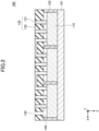
- FIG. 2 is a view illustrating an example of a cross-sectional configuration of the semiconductor device 100 according to the embodiment. In FIG. 2 , the semiconductor device 100 illustrated in FIG. 1 is illustrated upside down.
- the wireless communication device 200 includes the semiconductor device 100, a circuit board 210, and an antenna 220.
- the semiconductor device 100 includes a heat sink 101, a semiconductor element 110, a mold resin 120, a redistribution layer 130, and a cavity 140.
- the semiconductor device 100 is connected to an interconnect layer 211 on the surface of the circuit board 210 in the +Z direction by, for example, a bump 133 made of solder. That is, the semiconductor device 100 is flip-chip mounted on the circuit board 210.
- a bump 133 made of solder
- the circuit board 210 of the wireless communication device 200 is, for example, a high-frequency circuit board capable of transmitting signals in an ultra-high frequency band exceeding 100 GHz, and includes the interconnect layer 211 on surfaces and an inner layer on the ⁇ Z direction sides.
- an antenna 220 is formed at the end of the circuit board 210 in the -X direction.
- the antenna 220 is connected to the semiconductor device 100 through the interconnect layer 211 of the circuit board 210.
- the antenna 220 is, for example, a phased array antenna having directivity in the -X direction.
- FIG. 1 illustrates, as an example, a configuration in which three semiconductor elements 110 of the semiconductor device 100 are a power amplifier (PA), a mixer, and a phase shifter.
- the semiconductor elements 110 are not limited to the PA, the mixer, and the phase shifter.
- the wireless communication device 200 having such a configuration can amplify a signal by the PA, mix the signal with a local signal by the mixer, shift the phase of the signal by the phase shifter, and transmit the signal from the antenna 220.
- the wireless communication device 200 can receive a signal in the ultra-high frequency band.
- the wireless communication device 200 can be used as, for example, base stations of mobile communication systems for beyond 5G (fifth generation)/6G (sixth generation).
- a mobile communication system for Beyond 5G/6G realization of high-speed and large-capacity communication (5G or more) that greatly exceeds 100 Gbps is required.
- WPAN wireless personal area network
- it may be expected to transmit advanced video data such as high-definition moving images or holograms exceeding 8K to individual users to perform, for example, remote medical care or remote control in factories or the like.
- advanced video data such as high-definition moving images or holograms exceeding 8K
- an increase in transmission speed may be essential, and the use of "terahertz waves" around 300 GHz, which have a wider bandwidth than related-art microwaves or millimeter waves, may be suggested.
- CMOS complementary metal oxide semiconductor
- SiGe amplifier SiGe amplifier
- a communication distance is extended and directivity of radio waves is improved by using a high-power amplifier, to which a compound semiconductor such as gallium nitride (GaN) or indium phosphide (InP) is applied, to integrate these elements with an antenna to form an array.
- a high-power amplifier to which a compound semiconductor such as gallium nitride (GaN) or indium phosphide (InP) is applied, to integrate these elements with an antenna to form an array.
- GaN gallium nitride
- InP indium phosphide
- the application of the semiconductor device 100 is not limited to the mobile communication system for beyond 5G/6G as described above, but may be suitable for a wireless communication system that handles a signal in an ultra-high frequency band exceeding 100 GHz, for example.
- the semiconductor device 100 includes a plurality of semiconductor elements 110.
- the semiconductor element 110 is a semiconductor chip that is singulated, and may be an element including various semiconductor circuits, not limited to the PA, the mixer, and the phase shifter.
- the semiconductor device 100 may include at least one semiconductor element 110, and any number of semiconductor elements 110 may be used.
- the semiconductor element 110 is implemented by a GaN HEMT (High Electron Mobility Transistor) which is a GaN-based compound semiconductor, for example.
- GaN HEMT High Electron Mobility Transistor
- a single common heat sink 101 is connected to the surfaces of all the semiconductor elements 110 on the +Z direction side.
- the heat sink 101 is located on the semiconductor elements 110 in the state illustrated in FIG. 1 , and releases heat generated by the semiconductor elements 110 into the air.
- the heat sink 101 is made of metal or ceramic, for example.
- the side surfaces of the semiconductor elements 110 are covered with the mold resin 120.
- side surfaces of the semiconductor elements 110 on the ⁇ X direction sides are covered with the mold resin 120, but the side surfaces on the +Y direction side and/or side surfaces on the -Y direction side may also be covered with the mold resin 120.
- the plurality of semiconductor elements 110 are fixed by the mold resin 120.
- a plurality of pads are provided on the surface of the semiconductor elements 110 on the -Z direction side, and a redistribution interconnect 131 of the redistribution layer 130 is connected to each pad.
- the redistribution layer 130 is an example of an interconnect layer
- the redistribution interconnect 131 is an example of an interconnect.
- a cavity 140 is provided between all the semiconductor elements 110 and the redistribution layer 130. That is, the surfaces of all the semiconductor elements 110 on the -Z direction side are not covered with the redistribution layer 130, but are provided with the cavities 140. This configuration is to reduce the parasitic capacitance of the semiconductor element 110 and the redistribution interconnect 131.
- the mold resin 120 is fixed to the side surfaces of all the semiconductor elements 110.
- the position of the end portion of the mold resin 120 on the +Z direction side is equal to and flush with the position of the surface of each semiconductor element 110 on the +Z direction side.
- the end portion of the mold resin 120 on the -Z direction side protrudes more toward the -Z direction side than the surface of the semiconductor element 110 on the -Z direction side, and supports the surface of the interlayer insulating film 132 of the redistribution layer 130 on the +Z direction side.
- the interlayer insulating film 132 is an example of an insulating layer.
- the surface of the interlayer insulating film 132 on the +Z direction side is the surface of the redistribution layer 130 on the +Z direction side.
- the cavity 140 is provided between the surface of the redistribution layer 130 on the +Z direction side (the surface of the interlayer insulating film 132 on the +Z direction side) and the surface of the semiconductor element 110 on the -Z direction side.
- the mold resin 120 supports the redistribution layer 130 with respect to the semiconductor element 110.
- a thermosetting resin such as an epoxy resin can be used.
- the redistribution layer 130 includes a redistribution interconnect 131, an interlayer insulating film 132, and a through hole 135.
- the redistribution layer 130 is formed on the -Z direction side of the semiconductor element 110 fixed by the mold resin 120, for example.
- the cavity 140 is provided between the surface of the redistribution layer 130 on the +Z direction side (the surface of the interlayer insulating film 132 on the +Z direction side) and the surface of the semiconductor element 110 on the -Z direction side.
- the end portion of the redistribution interconnect 131 on the +Z direction side is connected to the pad of the semiconductor element 110 through the inside of the cavity 140.
- the redistribution interconnect 131 can be made of a metal such as copper, for example, and the interlayer insulating film 132 can be made of a photosensitive resin such as photosensitive polyimide.
- the through hole 135 penetrates a portion of the interlayer insulating film 132 of the redistribution layer 130 on the -Z direction side of the cavity 140 in the Z direction to communicate with the cavity 140.
- the through hole 135 is provided for injecting an etching solution or the like when a sacrificial film for forming the cavity 140 is removed.
- the sacrificial film is removed by injecting an etching solution such as N-methyl-2-pyrrolidone (NMP) into the through hole 135 to form the cavity 140.
- NMP N-methyl-2-pyrrolidone
- dry etching using ultraviolet light may be performed instead of the above-described wet etching. In this case, the reaction can be promoted when the redistribution layer 130 has the through hole 135, but the redistribution layer 130 may not have the through hole 135.
- the through hole 135 may penetrate a portion of the interlayer insulating film 132 other than the portion on the -Z direction side of the cavity 140.
- the through hole 135 may be bent in partway-through.
- FIG. 2 illustrates one through hole 135 provided corresponding to the leftmost semiconductor element 110 of the three semiconductor elements 110, it is preferable that each semiconductor element 110 be provided with at least one through hole 135. Such a configuration enables the sacrificial film to be removed more reliably.
- the cavity 140 is provided between the surface of the redistribution layer 130 on the +Z direction side (the surface of the interlayer insulating film 132 on the +Z direction side) and the surface of the semiconductor element 110 on the -Z direction side. Since air is present in the cavity 140, the relative dielectric constant at a portion on the surface side of the semiconductor element 110 on the -Z direction side can be reduced, compared to the case where an insulating material such as the interlayer insulating film 132 is present in place of the cavity. Thereby, the parasitic capacitance at the portion on the surface side of the semiconductor element 110 on the -Z direction side and at the redistribution interconnect 131 can be reduced.
- each semiconductor element 110 is provided with one cavity 140.
- This configuration enables both securing the strength of the redistribution layer 130 and reducing the parasitic capacitance.
- each cavity 140 is preferably provided with one through hole 135. This configuration enables the sacrificial film to be removed more reliably.
- the relative dielectric constant at a portion on the surface side of the semiconductor element 110 on the -Z direction side can be reduced.
- the cavity 140 covers the entire surfaces of the semiconductor elements 110 on the -Z direction side; however, of the surfaces of the semiconductor elements 110 in a plan view, the cavity 140 may be provided at least in a transistor region where a transistor is present or in an interconnect region where the redistribution interconnect 131 of the semiconductor element 110 is connected.
- the cavity 140 having a minimum size can reliably reduce the parasitic capacitance of the semiconductor element 110 and the redistribution interconnect 131, and both the strength of the redistribution layer 130 and the reduction in the parasitic capacitance can be achieved.
- the parasitic capacitance of the semiconductor element 110 and the redistribution interconnect 131 can be reliably reduced, and the propagation delay of a signal in the redistribution interconnect 131 can be inhibited.
- a region in which the redistribution interconnect 131 is connected to the surface of each semiconductor element 110 on the -Z direction side in FIG. 2 is the interconnect region. Since a transistor of the semiconductor element 110 is not illustrated in FIG. 2 , illustration of the transistor region is omitted in FIG. 2 . The transistor region and the interconnect region may overlap each other. The transistor region will be described later with reference to FIG. 3 .
- FIG. 3 is a view illustrating an example of a more specific cross-sectional configuration of the semiconductor device 100.
- FIG. 3 further illustrates as a more specific configuration of the semiconductor device 100, a gate 111G, a source 111S, a drain 111D, an insulating layer 112, a protection layer 113, a resistor 114A, a terminal 114B, a MIM (Metal Insulator Metal) capacitor 115, a via 136, a protection layer 137, and a scribe line 105.
- the via 136 is an example of a metallic layer.
- the gate 111G, the source 111S, the drain 111D, the insulating layer 112, the protection layer 113, the resistor 114A, the terminal 114B, and the MIM capacitor 115 are components of the semiconductor element 110.
- the via 136 and the protection layer 137 are included in the redistribution layer 130. That is, the redistribution layer 130 includes the redistribution interconnect 131, the interlayer insulating film 132, the through hole 135, the via 136, and the protection layer 137.
- the scribe line 105 is a component of the semiconductor device 100.
- the gate 111G, the source 111S, and the drain 111D are provided on the surface of the semiconductor element 110 on the -Z direction side, for example.
- a region where the gate 111G, the source 111S, and the drain 111D are provided is the transistor region. Note that the interval between the gate 111G and the drain 111D in the Y direction is longer than the interval between the gate 111G and the source 111S in the Y direction.
- the cavity 140 illustrated in FIG. 3 surrounds the gate 111G, and the gate 111G is exposed in the cavity 140, for example.
- the parasitic capacitance at the gate 111G of the semiconductor element 110 and in the vicinity thereof can be reliably reduced, and the loss in the switching operation of the transistor can be reduced.
- the cavity 140 is provided in the transistor region including a portion between the gate 111G and the source 111S and a portion between the gate 111G and the drain 111D in a plan view.
- the respective redistribution interconnects 131 connected to the source 111S and the drain 111D on the -Z direction side are not exposed in the cavity 140, but may be exposed.
- the through hole 135 is indicated by a broken line because the through hole 135 is located at a position more toward the +Y direction side than the position in the cross section in the Y direction illustrated in FIG. 3 , as an example.
- the insulating layer 112 is an insulating layer formed by, for example, ion implantation on the surface of the semiconductor element 110 on the -Z direction side.
- the insulating layer 112 is formed in a portion other than the transistor region.
- the protection layer 113 is an insulating layer provided on the -Z direction side of the redistribution layer 130, and is a surface protection layer that protects the surface of the semiconductor element 110.
- the protection layer 113 is made of SiN, for example.
- the protection layer 113 covers a contact portion of the base of the gate 111G with the semiconductor element 110, surfaces of the source 111S, the drain 111D, and the insulating layer 112 on the - Z direction side, the resistor 114A, the terminal 114B, the electrodes 115A and 115B of the MIM capacitor 115, and the like.
- the resistor 114A, the terminal 114B, the MIM capacitor 115, and the via 136 are connected to the redistribution interconnects 131 as illustrated in FIG. 3 as an example.
- the protection layer 137 is made of SiN, for example, and covers the surface of the redistribution layer 130 on the -Z direction side.
- the scribe line 105 is provided at the end portion of the semiconductor device 100 in the -X direction.
- the protection layer 113 is provided on the surface of the semiconductor element 110 on the -Z direction side.
- the protection layer 113 is a SiN film that protects the surface of the semiconductor element 110. Since the protection layer 113 is much thinner than the interlayer insulating film 132, the parasitic capacitance due to the presence of the protection layer 113 is small.
- the semiconductor device 100 has a configuration in which the heat sink 101 is directly connected to the surface of the semiconductor element 110 on the +Z direction side, and therefore, heat generated by the operation of the semiconductor element 110 can be released into the air through the heat sink 101.
- the temperature of the semiconductor element 110 is lowered, and thus, the distortion of the redistribution layer 130 can be reduced.
- the redistribution layer 130 is supported by the mold resin 120 with respect to the semiconductor element 110, distortion due to heat generated by the semiconductor element 110 is prevented, and the semiconductor device 100 can stably operate for a long period of time.
- the through hole 135 may penetrate a portion of the interlayer insulating film 132 other than the portion on the -Z direction side of the cavity 140.
- a through hole that connects the through hole for forming the via 136 and the cavity 140 in the X direction may be formed.
- the cavity 140 is connected to the outside via the through hole extending in the X direction and the through hole for forming the via 136.
- the via 136 is formed, only the inside of the through hole for forming the via 136 is filled with the metallic layer of the via 136, and the metallic layer is not formed in the through hole extending in the X direction.
- the metallic layer is formed in at least a part of the through hole that connects the cavity 140 to the outside of the redistribution layer 130, and thus it is possible to prevent moisture from entering the cavity 140.
- the via 136 may be formed in a cylindrical shape in the through hole penetrating the interlayer insulating film 132 in the Z direction to completely fill the through hole, or may be formed in a cylindrical shape along the inner surface of the through hole to not completely fill the through hole.
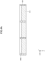
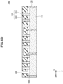
- FIGS. 4A to 4D are views illustrating an example of a method for fabricating the semiconductor device 100.
- a structure is prepared in which a laminate is obtained by forming the sacrificial film 140A on the surface of the semiconductor element 110 on the -Z direction side and side surfaces of the laminate are fixed by the mold resin 120.
- the structure illustrated in FIG. 4A can be obtained by forming the sacrificial film 140A on a surface of a unsingulated semiconductor element 110 on the -Z direction side, then performing singulation, forming a mold resin on side surfaces of the singulated semiconductor elements using a mold, and polishing and planarizing the surfaces on the +Z direction side and the -Z direction side.
- the sacrificial film 140A may be made of a material that is decomposed by light such as ultraviolet rays.
- the sacrificial film 140A may be made of a sacrificial film material corresponding to the GaN semiconductor.
- a sacrificial film material corresponding to the GaN semiconductor an organic layer that is decomposed by ultraviolet rays having wavelengths of 300 nm to 400 nm and includes oxygen-containing functional groups (carbonyl groups (CoS), carboxyl groups (COOH), hydroxyl groups (OH), and the like) may be used, for example.
- oxygen-containing functional groups carbonyl groups (CoS), carboxyl groups (COOH), hydroxyl groups (OH), and the like
- Examples of such an organic layer include methyl glutarimide, polymethyl methacrylate, polypropylene, and polycarbonate.
- the redistribution interconnect 131 and the interlayer insulating film 132 of the redistribution layer 130 are formed on the surface of the structure illustrated in FIG. 4A on the -Z direction side.
- the redistribution interconnect 131 is connected to a pad on the surface of the semiconductor element 110 on the -Z direction side after removing a part of the sacrificial film 140A by using a lithography technique.
- the redistribution interconnect 131 can be fabricated by forming a copper interconnect by a plating process.
- the interlayer insulating film 132 can be formed by forming a SiO 2 film, for example.
- the through hole 135 is formed in the interlayer insulating film 132 of the redistribution layer 130 illustrated in FIG. 4C .
- the through hole 135 may be formed by, for example, dry etching or wet etching using a photolithography technique.
- dry etching ICP-RIE (Inductive Coupled Plasma Reactive Ion Etching) using a gas mixture of helium (He) and sulfurhexafluoride (SF 6 ), tetrafluoromethane (CF 4 ), or trifluoromethane (CHF 3 ) can be used.
- SF 6 is most preferable.
- the cavity 140 can be formed in the place where the sacrificial film 140A was present.
- dry etching using ultraviolet rays may be performed instead of wet etching.
- the reaction can be promoted when the redistribution layer 130 has the through hole 135, however, the redistribution layer 130 may not have the through hole 135.
- FIG. 5A is a view illustrating an example of a cross-sectional configuration of the semiconductor device 10 according to a comparative example.
- FIG. 5B is a view illustrating an example of a cross-sectional configuration of the semiconductor device 100 according to the embodiment.
- a semiconductor element 110, a gate 111G, a source 111S, a drain 111D, an interlayer insulating film 132, a protection layer 113, and a cavity 140 are illustrated as components of the semiconductor device 100 according to the embodiment.
- the semiconductor device 10 according to the comparative example illustrated in FIG. 5A has a configuration in which the cavity 140 is removed from the semiconductor device 100 of the embodiment illustrated in FIG.
- the gate 111G, the source 111S, the drain 111D, and the protection layer 113 are covered with the interlayer insulating film 132. Since the cavity 140 is not provided in the semiconductor device 10 according to the comparative example, the parasitic capacitance of the semiconductor element 110 is larger than that of the semiconductor device 100 of the embodiment.
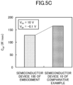
- FIG. 5C is a graph illustrating examples of experimental results.
- the electrostatic capacitance C gd between the gate 111G and the drain 111D of the semiconductor device 10 according to the comparative example illustrated in FIG. 5A and the electrostatic capacitance C gd between the gate 111G and the drain 111D of the semiconductor device 100 of the embodiment illustrated in FIG. 5B were measured, and the results indicate that the electrostatic capacitance C gd of the semiconductor device 100 of the embodiment was reduced by approximately 20%.
- the electrostatic capacitance C gd of the semiconductor device 100 of the embodiment was approximately 130 (fF/mm), and the electrostatic capacitance C gd between the gate 111G and the drain 111D of the semiconductor device 10 according to the comparative example was approximately 170 (fF/mm).
- the measurements were performed by setting the voltage V gs between the gate 111G and the source 111S to -0.1 V, and setting the voltage V ds between the drain 111D and the source 111S to 10 V.
- the results also indicate that the electrostatic capacitance C gs between the gate 111G and the source 111S of the semiconductor device 100 of the embodiment was reduced by approximately 20%.
- the results indicate that the parasitic capacitance of the semiconductor element 110 can be reduced by providing the cavity 140 between the semiconductor element 110 and the redistribution layer 130.
- the parasitic capacitance of the semiconductor element 110 By reducing the parasitic capacitance of the semiconductor element 110, the transmission loss and transmission delay of signals in the semiconductor element 110 can be reduced, and excellent operation characteristics of the semiconductor element 110 capable of handling ultra-high frequencies can be obtained.
- FIG. 6 is a view illustrating an example of a cross-sectional configuration of a semiconductor device 100A according to a modification of the embodiment.
- the semiconductor device 100A is different from the semiconductor device 100 illustrated in FIG. 2 in that a metallic layer 135A is provided inside the through hole 135.
- the metallic layer 135A may be included in the redistribution layer 130 and may be connected to the redistribution interconnect 131; however, the metallic layer 135A may be a dummy pattern that is not connected to the redistribution interconnect 131.
- the metallic layer 135A is made of copper, for example, as in the redistribution interconnect 131, and can be produced by a plating process.
- the metallic layer 135A plugs the through hole 135. Therefore, it is possible to prevent moisture from entering the cavity 140 from the outside of the cavity 140. By plugging the through hole 135 with the metallic layer 135A, it is possible to more reliably prevent moisture from entering the cavity 140, and the semiconductor element 110 can operate more stably over a long period of time. As illustrated in FIG. 6 , the metallic layer 135A need not necessarily plug the through hole 135 completely, and the metallic layer 135A may be provided in at least a part of the through hole 135. With such a configuration, it is possible to prevent moisture from entering the cavity 140, and the semiconductor element 110 can stably operate for a long period of time.
- a semiconductor device 100 includes a semiconductor element 110; a redistribution layer 130 provided on a first surface side of the semiconductor element 110, the redistribution layer 130 including a redistribution interconnect 131 connected to the semiconductor element 110 and an interlayer insulating film 132 covering the redistribution interconnect 131; and a cavity 140 provided between the first surface of the semiconductor element 110 and the redistribution layer 130. Therefore, the first surface (the surface on the -Z direction side) of the semiconductor element 110 faces the cavity 140, and the parasitic capacitance of the semiconductor element 110 can be reduced.
- the semiconductor device 100 with the reduced parasitic capacitance of the semiconductor element 110 can be provided.
- the redistribution layer 130 may further include a through hole 135 that penetrates the interlayer insulating film 132 and communicates with the cavity 140.
- the cavity 140 can be formed by injecting an etching solution or the like through the through hole 135.
- the cavity 140 may be provided in a transistor region where a transistor of the semiconductor element 110 is present or in an interconnect region where the redistribution interconnect 131 is connected to the semiconductor element 110 in a plan view.
- the parasitic capacitance of the semiconductor element 110 or the redistribution interconnect 131 can be reliably reduced by providing the cavity 140 having a minimum size, and both the strength of the redistribution layer 130 and the reduction in the parasitic capacitance can be achieved.
- the cavity 140 is provided in the interconnect region in a plan view, the parasitic capacitance of the semiconductor element 110 and the redistribution interconnect 131 can be reliably reduced, and the transmission delay of a signal in the redistribution interconnect 131 can be prevented.
- the cavity 140 may surround the gate 111G of the transistor. Therefore, the parasitic capacitance at the gate 111G of the semiconductor element 110 and in the vicinity thereof can be reliably reduced, and the loss in the switching operation of the transistor can be reduced.
- the semiconductor device 100 may include a plurality of semiconductor elements 110 and a plurality of cavities 140, and one cavity 140 may be provided in each semiconductor element 110.
- the size of the cavity 140 can be minimized, and it is possible to achieve both securing the strength of the redistribution layer 130 and reduction in the parasitic capacitance.
- the semiconductor device may include a plurality of semiconductor elements 110 and further include a mold resin 120 provided on side surfaces of the plurality of semiconductor elements 110, and the mold resin 120 may support the redistribution layer 130 with respect to the semiconductor elements 110.
- the mold resin 120 By providing the mold resin 120 on the side surface of each semiconductor element 110, the strength of the redistribution layer 130 can be secured in the configuration including the plurality of semiconductor elements 110.
- the semiconductor device may further include a metallic layer 135A or a via 136 provided in at least a part of the through hole 135.
- a metallic layer 135A or a via 136 provided in at least a part of the through hole 135.
- the semiconductor device 100 may further include a heat sink 101 provided on a second surface (surface on the +Z direction side) opposite to the first surface (surface on the -Z direction side) of the semiconductor element 110.
- This configuration enables cooling of the semiconductor element 110, and also achieves both stable operation of the semiconductor element 110 and prevention of distortion of the redistribution layer 130 due to heat.
- a wireless communication device 200 includes a semiconductor element 110; a redistribution layer 130 provided on a first surface side of the semiconductor element 110, the redistribution layer 130 including a redistribution interconnect 131 connected to the semiconductor element 110 and an interlayer insulating film 132 covering the redistribution interconnect 131; a cavity 140 provided between the first surface of the semiconductor element 110 and the redistribution layer 130, a circuit board 210 provided opposite to the semiconductor element 110 with respect to the redistribution layer 130, the circuit board 210 being connected to the redistribution layer 130; and an antenna 220 provided on the circuit board 210.
- the first surface (the surface on the -Z direction side) of the semiconductor element 110 faces the cavity 140, and the parasitic capacitance of the semiconductor element 110 can be reduced.
- the wireless communication device 200 with the reduced parasitic capacitance of the semiconductor element 110 can be provided.
- a method for fabricating a semiconductor device includes forming a sacrificial film 140A on a first surface of a semiconductor element 110; forming a redistribution layer 130 on the sacrificial film 140A, the redistribution layer 130 including a redistribution interconnect 131 connected to the semiconductor element 110 and an interlayer insulating film 132 covering the redistribution interconnect 131; and removing the sacrificial film 140A to form a cavity 140 between the first surface of the semiconductor element 110 and the redistribution layer 130.
- the first surface (the surface on the -Z direction side) of the semiconductor element 110 faces the cavity 140, and the parasitic capacitance of the semiconductor element 110 can be reduced.
- the method for fabricating a semiconductor device with the reduced parasitic capacitance of the semiconductor element 110 can be provided.
Landscapes
- Engineering & Computer Science (AREA)
- Microelectronics & Electronic Packaging (AREA)
- Internal Circuitry In Semiconductor Integrated Circuit Devices (AREA)
- Cooling Or The Like Of Semiconductors Or Solid State Devices (AREA)
- Manufacturing & Machinery (AREA)
- Physics & Mathematics (AREA)
- Geometry (AREA)
Abstract
Description
- The disclosures discussed herein relate to a semiconductor device, a wireless communication device, and a method for fabricating the semiconductor device.
- In the related art, a semiconductor device including a redistribution layer and a photosensitive ink layer that are provided on an image sensing chip has been proposed. In such a semiconductor device, the image sensing chip has a hollow opening, the redistribution layer extends inside the hollow opening, and a cavity is provided above the redistribution layer (for example, see
Japanese National Publication of International Patent Application No. 2018-533225 - In such a related art semiconductor device, an upper surface of the image sensing chip (a semiconductor element) is covered with the redistribution layer and the photosensitive ink layer, and thus the parasitic capacitance of the semiconductor element is large.
- Accordingly, it appears desirable to provide a semiconductor device with reduced parasitic capacitance of a semiconductor element, a wireless communication device, and a method for fabricating the semiconductor device.
- According to an aspect of an embodiment of the present disclosure, a semiconductor device includes:
- a semiconductor element;
- an interconnect layer provided on a first surface side of the semiconductor element, the interconnect layer including an interconnect connected to the semiconductor element and an insulating layer covering the interconnect; and
- a cavity provided between the first surface of the semiconductor element and the interconnect layer.
- The embodiment of the present disclosure can provide a semiconductor device with reduced parasitic capacitance of a semiconductor element, a wireless communication device, and a method of fabricating the semiconductor device.
- The object and advantages of the invention will be realized and attained by means of the elements and combinations particularly pointed out in the claims.
- It is to be understood that both the foregoing general description and the following detailed description are exemplary and explanatory and are not restrictive of the invention, as claimed.
-
-
FIG. 1 is a view illustrating an example of a cross-sectional configuration of awireless communication device 200 including asemiconductor device 100 according to an embodiment. -
FIG. 2 is a view illustrating an example of a cross-sectional configuration of thesemiconductor device 100 according to the embodiment. -
FIG. 3 is a view illustrating an example of a more specific cross-sectional configuration of thesemiconductor device 100. -
FIG. 4A is a view illustrating an example of a method for fabricating thesemiconductor device 100. -
FIG. 4B is a view illustrating an example of the method for fabricating thesemiconductor device 100. -
FIG. 4C is a view illustrating an example of the method for fabricating thesemiconductor device 100. -
FIG. 4D is a view illustrating an example of the method for fabricating thesemiconductor device 100. -
FIG. 5A is a view illustrating an example of a cross-sectional configuration of asemiconductor device 10 according to a comparative example. -
FIG. 5B is a view illustrating an example of a cross-sectional configuration of thesemiconductor device 100 according to the embodiment. -
FIG. 5C is a graph illustrating an example of experimental results. -
FIG. 6 is a view illustrating an example of a cross-sectional configuration of asemiconductor device 100A according to a modification of the embodiment. - Hereinafter, an embodiment to which a semiconductor device, a wireless communication device, and a method for fabricating the semiconductor device according to the present disclosure are applied will be described with reference to the accompanying drawings. In the following description, the same elements are denoted by the same reference numerals, and redundant description may be omitted.
- In the following description, an XYZ coordinate system is defined. A direction parallel to the X-axis (X direction), a direction parallel to the Y-axis (Y direction), and a direction parallel to the Z-axis (Z direction) are orthogonal to each other. The X direction is an example of a first axis direction, the Y direction is an example of a second axis direction, and the Z direction is an example of a third axis direction. Further, the plan view means an XY plane view.
- In the following description, the length, thickness, and the like of each portion may be exaggerated to facilitate the understanding of the configuration. In addition, the terms "parallel", "perpendicular", "orthogonal", "horizontal", "vertical", "upper", "lower", and the like allow a deviation to the extent that the effect of the embodiment is not impaired.
-
FIG. 1 is a view illustrating an example of a cross-sectional configuration of awireless communication device 200 including asemiconductor device 100 according to an embodiment.FIG. 2 is a view illustrating an example of a cross-sectional configuration of thesemiconductor device 100 according to the embodiment. InFIG. 2 , thesemiconductor device 100 illustrated inFIG. 1 is illustrated upside down. - The
wireless communication device 200 includes thesemiconductor device 100, acircuit board 210, and anantenna 220. Thesemiconductor device 100 includes aheat sink 101, asemiconductor element 110, amold resin 120, aredistribution layer 130, and acavity 140. Thesemiconductor device 100 is connected to aninterconnect layer 211 on the surface of thecircuit board 210 in the +Z direction by, for example, abump 133 made of solder. That is, thesemiconductor device 100 is flip-chip mounted on thecircuit board 210. Each of the components will be described below. - The
circuit board 210 of thewireless communication device 200 is, for example, a high-frequency circuit board capable of transmitting signals in an ultra-high frequency band exceeding 100 GHz, and includes theinterconnect layer 211 on surfaces and an inner layer on the ± Z direction sides. In addition, as an example, anantenna 220 is formed at the end of thecircuit board 210 in the -X direction. Theantenna 220 is connected to thesemiconductor device 100 through theinterconnect layer 211 of thecircuit board 210. Theantenna 220 is, for example, a phased array antenna having directivity in the -X direction. -
FIG. 1 illustrates, as an example, a configuration in which threesemiconductor elements 110 of thesemiconductor device 100 are a power amplifier (PA), a mixer, and a phase shifter. Thesemiconductor elements 110 are not limited to the PA, the mixer, and the phase shifter. Thewireless communication device 200 having such a configuration can amplify a signal by the PA, mix the signal with a local signal by the mixer, shift the phase of the signal by the phase shifter, and transmit the signal from theantenna 220. Thewireless communication device 200 can receive a signal in the ultra-high frequency band. Thewireless communication device 200 can be used as, for example, base stations of mobile communication systems for beyond 5G (fifth generation)/6G (sixth generation). - In a mobile communication system for Beyond 5G/6G, realization of high-speed and large-capacity communication (5G or more) that greatly exceeds 100 Gbps is required. For example, in a wireless personal area network (WPAN), which is one of the use cases, it may be expected to transmit advanced video data such as high-definition moving images or holograms exceeding 8K to individual users to perform, for example, remote medical care or remote control in factories or the like. In order to meet such expectations, an increase in transmission speed may be essential, and the use of "terahertz waves" around 300 GHz, which have a wider bandwidth than related-art microwaves or millimeter waves, may be suggested.
- When utilizing these ultra-high frequency radio waves, it may be considered desirable to use, in addition to the WPAN, a phased array antenna that directs a beam only in a necessary direction for securing a reaching distance of radio waves and reducing power consumption. However, it may be challenging to secure a communication range assumed in a use case with an output of an array antenna in a 300 GHz band using a complementary metal oxide semiconductor (CMOS) or SiGe amplifier which has been reported so far. Therefore, it is expected that a communication distance is extended and directivity of radio waves is improved by using a high-power amplifier, to which a compound semiconductor such as gallium nitride (GaN) or indium phosphide (InP) is applied, to integrate these elements with an antenna to form an array.
- In the ultra-high frequency band exceeding 100 GHz, it has been reported that a transmission loss of a signal in a solder or a wire bonding portion used for bonding between semiconductor elements in a front end of radio wave transmission and reception such as an amplifier, a mixer, and a phase shifter may adversely affect high-frequency characteristics of a module. As a countermeasure, a redistribution structure using a mold resin has been studied as a structure of a semiconductor device including a semiconductor element. However, when the surface of the semiconductor element is covered with the insulating layer for rewiring, the parasitic capacitance increases, and the high-frequency characteristics deteriorates. Therefore, it is desirable to lower the parasitic capacitance.
- In addition, heat generation becomes severe when rewiring a high-power amplifier. Therefore, it is desirable to implement a heat dissipation structure capable of preventing warpage of a semiconductor device including a semiconductor element.
- An example of a specific structure of the
semiconductor device 100 will be described below. The application of thesemiconductor device 100 is not limited to the mobile communication system for beyond 5G/6G as described above, but may be suitable for a wireless communication system that handles a signal in an ultra-high frequency band exceeding 100 GHz, for example. - As illustrated in
FIG. 2 , thesemiconductor device 100 includes a plurality ofsemiconductor elements 110. Thesemiconductor element 110 is a semiconductor chip that is singulated, and may be an element including various semiconductor circuits, not limited to the PA, the mixer, and the phase shifter. Thesemiconductor device 100 may include at least onesemiconductor element 110, and any number ofsemiconductor elements 110 may be used. Thesemiconductor element 110 is implemented by a GaN HEMT (High Electron Mobility Transistor) which is a GaN-based compound semiconductor, for example. - As an example, a single
common heat sink 101 is connected to the surfaces of all thesemiconductor elements 110 on the +Z direction side. Theheat sink 101 is located on thesemiconductor elements 110 in the state illustrated inFIG. 1 , and releases heat generated by thesemiconductor elements 110 into the air. Theheat sink 101 is made of metal or ceramic, for example. - The side surfaces of the
semiconductor elements 110 are covered with themold resin 120. In the XZ cross-section illustrated inFIG. 2 , side surfaces of thesemiconductor elements 110 on the ±X direction sides are covered with themold resin 120, but the side surfaces on the +Y direction side and/or side surfaces on the -Y direction side may also be covered with themold resin 120. The plurality ofsemiconductor elements 110 are fixed by themold resin 120. - A plurality of pads (not illustrated) are provided on the surface of the
semiconductor elements 110 on the -Z direction side, and aredistribution interconnect 131 of theredistribution layer 130 is connected to each pad. Theredistribution layer 130 is an example of an interconnect layer, and theredistribution interconnect 131 is an example of an interconnect. Acavity 140 is provided between all thesemiconductor elements 110 and theredistribution layer 130. That is, the surfaces of all thesemiconductor elements 110 on the -Z direction side are not covered with theredistribution layer 130, but are provided with thecavities 140. This configuration is to reduce the parasitic capacitance of thesemiconductor element 110 and theredistribution interconnect 131. - The
mold resin 120 is fixed to the side surfaces of all thesemiconductor elements 110. The position of the end portion of themold resin 120 on the +Z direction side is equal to and flush with the position of the surface of eachsemiconductor element 110 on the +Z direction side. The end portion of themold resin 120 on the -Z direction side protrudes more toward the -Z direction side than the surface of thesemiconductor element 110 on the -Z direction side, and supports the surface of theinterlayer insulating film 132 of theredistribution layer 130 on the +Z direction side. Theinterlayer insulating film 132 is an example of an insulating layer. The surface of theinterlayer insulating film 132 on the +Z direction side is the surface of theredistribution layer 130 on the +Z direction side. In this way, thecavity 140 is provided between the surface of theredistribution layer 130 on the +Z direction side (the surface of theinterlayer insulating film 132 on the +Z direction side) and the surface of thesemiconductor element 110 on the -Z direction side. In the portion of thecavity 140, themold resin 120 supports theredistribution layer 130 with respect to thesemiconductor element 110. As a material of themold resin 120, a thermosetting resin such as an epoxy resin can be used. - The
redistribution layer 130 includes aredistribution interconnect 131, aninterlayer insulating film 132, and a throughhole 135. Theredistribution layer 130 is formed on the -Z direction side of thesemiconductor element 110 fixed by themold resin 120, for example. As described above, thecavity 140 is provided between the surface of theredistribution layer 130 on the +Z direction side (the surface of theinterlayer insulating film 132 on the +Z direction side) and the surface of thesemiconductor element 110 on the -Z direction side. The end portion of theredistribution interconnect 131 on the +Z direction side is connected to the pad of thesemiconductor element 110 through the inside of thecavity 140. Theredistribution interconnect 131 can be made of a metal such as copper, for example, and theinterlayer insulating film 132 can be made of a photosensitive resin such as photosensitive polyimide. - The through
hole 135 penetrates a portion of theinterlayer insulating film 132 of theredistribution layer 130 on the -Z direction side of thecavity 140 in the Z direction to communicate with thecavity 140. The throughhole 135 is provided for injecting an etching solution or the like when a sacrificial film for forming thecavity 140 is removed. The sacrificial film is removed by injecting an etching solution such as N-methyl-2-pyrrolidone (NMP) into the throughhole 135 to form thecavity 140. Note that dry etching using ultraviolet light may be performed instead of the above-described wet etching. In this case, the reaction can be promoted when theredistribution layer 130 has the throughhole 135, but theredistribution layer 130 may not have the throughhole 135. - Note that the configuration in which the through
hole 135 penetrates the portion of theinterlayer insulating film 132 on the -Z direction side of thecavity 140 in the Z direction has been described here. However, the throughhole 135 may penetrate a portion of theinterlayer insulating film 132 other than the portion on the -Z direction side of thecavity 140. The throughhole 135 may be bent in partway-through. - Although
FIG. 2 illustrates one throughhole 135 provided corresponding to theleftmost semiconductor element 110 of the threesemiconductor elements 110, it is preferable that eachsemiconductor element 110 be provided with at least one throughhole 135. Such a configuration enables the sacrificial film to be removed more reliably. - The
cavity 140 is provided between the surface of theredistribution layer 130 on the +Z direction side (the surface of theinterlayer insulating film 132 on the +Z direction side) and the surface of thesemiconductor element 110 on the -Z direction side. Since air is present in thecavity 140, the relative dielectric constant at a portion on the surface side of thesemiconductor element 110 on the -Z direction side can be reduced, compared to the case where an insulating material such as theinterlayer insulating film 132 is present in place of the cavity. Thereby, the parasitic capacitance at the portion on the surface side of thesemiconductor element 110 on the -Z direction side and at theredistribution interconnect 131 can be reduced. - The
cavity 140 is divided in the X direction by themold resin 120, and eachsemiconductor element 110 is provided with onecavity 140. This configuration enables both securing the strength of theredistribution layer 130 and reducing the parasitic capacitance. In the configuration in which eachsemiconductor element 110 is provided with onecavity 140, eachcavity 140 is preferably provided with one throughhole 135. This configuration enables the sacrificial film to be removed more reliably. - In
FIG. 2 , the relative dielectric constant at a portion on the surface side of thesemiconductor element 110 on the -Z direction side can be reduced. Thecavity 140 covers the entire surfaces of thesemiconductor elements 110 on the -Z direction side; however, of the surfaces of thesemiconductor elements 110 in a plan view, thecavity 140 may be provided at least in a transistor region where a transistor is present or in an interconnect region where theredistribution interconnect 131 of thesemiconductor element 110 is connected. Thecavity 140 having a minimum size can reliably reduce the parasitic capacitance of thesemiconductor element 110 and theredistribution interconnect 131, and both the strength of theredistribution layer 130 and the reduction in the parasitic capacitance can be achieved. In addition, when thecavity 140 is provided in the interconnect region in a plan view, the parasitic capacitance of thesemiconductor element 110 and theredistribution interconnect 131 can be reliably reduced, and the propagation delay of a signal in theredistribution interconnect 131 can be inhibited. - A region in which the
redistribution interconnect 131 is connected to the surface of eachsemiconductor element 110 on the -Z direction side inFIG. 2 is the interconnect region. Since a transistor of thesemiconductor element 110 is not illustrated inFIG. 2 , illustration of the transistor region is omitted inFIG. 2 . The transistor region and the interconnect region may overlap each other. The transistor region will be described later with reference toFIG. 3 . -
FIG. 3 is a view illustrating an example of a more specific cross-sectional configuration of thesemiconductor device 100.FIG. 3 further illustrates as a more specific configuration of thesemiconductor device 100, agate 111G, asource 111S, adrain 111D, an insulatinglayer 112, aprotection layer 113, aresistor 114A, a terminal 114B, a MIM (Metal Insulator Metal)capacitor 115, a via 136, aprotection layer 137, and ascribe line 105. The via 136 is an example of a metallic layer. - Among these components, the
gate 111G, thesource 111S, thedrain 111D, the insulatinglayer 112, theprotection layer 113, theresistor 114A, the terminal 114B, and theMIM capacitor 115 are components of thesemiconductor element 110. The via 136 and theprotection layer 137 are included in theredistribution layer 130. That is, theredistribution layer 130 includes theredistribution interconnect 131, theinterlayer insulating film 132, the throughhole 135, the via 136, and theprotection layer 137. Thescribe line 105 is a component of thesemiconductor device 100. - The
gate 111G, thesource 111S, and thedrain 111D are provided on the surface of thesemiconductor element 110 on the -Z direction side, for example. In a plan view, a region where thegate 111G, thesource 111S, and thedrain 111D are provided is the transistor region. Note that the interval between thegate 111G and thedrain 111D in the Y direction is longer than the interval between thegate 111G and thesource 111S in the Y direction. - The
cavity 140 illustrated inFIG. 3 surrounds thegate 111G, and thegate 111G is exposed in thecavity 140, for example. The parasitic capacitance at thegate 111G of thesemiconductor element 110 and in the vicinity thereof can be reliably reduced, and the loss in the switching operation of the transistor can be reduced. - The
cavity 140 is provided in the transistor region including a portion between thegate 111G and thesource 111S and a portion between thegate 111G and thedrain 111D in a plan view. InFIG. 3 , the respective redistribution interconnects 131 connected to thesource 111S and thedrain 111D on the -Z direction side are not exposed in thecavity 140, but may be exposed. In the configuration illustrated inFIG. 3 , the throughhole 135 is indicated by a broken line because the throughhole 135 is located at a position more toward the +Y direction side than the position in the cross section in the Y direction illustrated inFIG. 3 , as an example. - The insulating
layer 112 is an insulating layer formed by, for example, ion implantation on the surface of thesemiconductor element 110 on the -Z direction side. The insulatinglayer 112 is formed in a portion other than the transistor region. - The
protection layer 113 is an insulating layer provided on the -Z direction side of theredistribution layer 130, and is a surface protection layer that protects the surface of thesemiconductor element 110. Theprotection layer 113 is made of SiN, for example. Theprotection layer 113 covers a contact portion of the base of thegate 111G with thesemiconductor element 110, surfaces of thesource 111S, thedrain 111D, and the insulatinglayer 112 on the - Z direction side, theresistor 114A, the terminal 114B, theelectrodes MIM capacitor 115, and the like. - The
resistor 114A, the terminal 114B, theMIM capacitor 115, and the via 136 are connected to the redistribution interconnects 131 as illustrated inFIG. 3 as an example. Theprotection layer 137 is made of SiN, for example, and covers the surface of theredistribution layer 130 on the -Z direction side. Thescribe line 105 is provided at the end portion of thesemiconductor device 100 in the -X direction. - As described above, in the
semiconductor device 100, thecavity 140 is provided between the surface of thesemiconductor element 110 on theredistribution layer 130 side and theinterlayer insulating film 132 of theredistribution layer 130 in the transistor region in plan view. Thus, the parasitic capacitance of thesemiconductor element 110 can be reduced in the transistor region. By reducing the parasitic capacitance of thesemiconductor element 110, the transmission loss and transmission delay of a signal in thesemiconductor element 110 can be reduced, and the operation characteristics of thesemiconductor element 110 can be improved. - Note that, also in the transistor region, the
protection layer 113 is provided on the surface of thesemiconductor element 110 on the -Z direction side. Theprotection layer 113 is a SiN film that protects the surface of thesemiconductor element 110. Since theprotection layer 113 is much thinner than the interlayer insulatingfilm 132, the parasitic capacitance due to the presence of theprotection layer 113 is small. - Further, as illustrated in
FIG. 2 , thesemiconductor device 100 has a configuration in which theheat sink 101 is directly connected to the surface of thesemiconductor element 110 on the +Z direction side, and therefore, heat generated by the operation of thesemiconductor element 110 can be released into the air through theheat sink 101. The temperature of thesemiconductor element 110 is lowered, and thus, the distortion of theredistribution layer 130 can be reduced. - Further, since the
redistribution layer 130 is supported by themold resin 120 with respect to thesemiconductor element 110, distortion due to heat generated by thesemiconductor element 110 is prevented, and thesemiconductor device 100 can stably operate for a long period of time. - The through
hole 135 may penetrate a portion of theinterlayer insulating film 132 other than the portion on the -Z direction side of thecavity 140. For example, a through hole that connects the through hole for forming the via 136 and thecavity 140 in the X direction may be formed. In this case, before the via 136 is formed, thecavity 140 is connected to the outside via the through hole extending in the X direction and the through hole for forming the via 136. When the via 136 is formed, only the inside of the through hole for forming the via 136 is filled with the metallic layer of the via 136, and the metallic layer is not formed in the through hole extending in the X direction. In this case, by forming the via 136, the metallic layer is formed in at least a part of the through hole that connects thecavity 140 to the outside of theredistribution layer 130, and thus it is possible to prevent moisture from entering thecavity 140. The via 136 may be formed in a cylindrical shape in the through hole penetrating theinterlayer insulating film 132 in the Z direction to completely fill the through hole, or may be formed in a cylindrical shape along the inner surface of the through hole to not completely fill the through hole. -
FIGS. 4A to 4D are views illustrating an example of a method for fabricating thesemiconductor device 100. - First, as illustrated in
FIG. 4A , a structure is prepared in which a laminate is obtained by forming thesacrificial film 140A on the surface of thesemiconductor element 110 on the -Z direction side and side surfaces of the laminate are fixed by themold resin 120. For example, the structure illustrated inFIG. 4A can be obtained by forming thesacrificial film 140A on a surface of aunsingulated semiconductor element 110 on the -Z direction side, then performing singulation, forming a mold resin on side surfaces of the singulated semiconductor elements using a mold, and polishing and planarizing the surfaces on the +Z direction side and the -Z direction side. Thesacrificial film 140A may be made of a material that is decomposed by light such as ultraviolet rays. For example, when thesemiconductor element 110 is a GaN semiconductor, thesacrificial film 140A may be made of a sacrificial film material corresponding to the GaN semiconductor. As the sacrificial film material corresponding to the GaN semiconductor, an organic layer that is decomposed by ultraviolet rays having wavelengths of 300 nm to 400 nm and includes oxygen-containing functional groups (carbonyl groups (CoS), carboxyl groups (COOH), hydroxyl groups (OH), and the like) may be used, for example. Examples of such an organic layer include methyl glutarimide, polymethyl methacrylate, polypropylene, and polycarbonate. - Next, as illustrated in
FIG. 4B , theredistribution interconnect 131 and theinterlayer insulating film 132 of theredistribution layer 130 are formed on the surface of the structure illustrated inFIG. 4A on the -Z direction side. Theredistribution interconnect 131 is connected to a pad on the surface of thesemiconductor element 110 on the -Z direction side after removing a part of thesacrificial film 140A by using a lithography technique. As an example, theredistribution interconnect 131 can be fabricated by forming a copper interconnect by a plating process. Theinterlayer insulating film 132 can be formed by forming a SiO2 film, for example. - Next, as illustrated in
FIG. 4B , the throughhole 135 is formed in theinterlayer insulating film 132 of theredistribution layer 130 illustrated inFIG. 4C . The throughhole 135 may be formed by, for example, dry etching or wet etching using a photolithography technique. As the dry etching, ICP-RIE (Inductive Coupled Plasma Reactive Ion Etching) using a gas mixture of helium (He) and sulfurhexafluoride (SF6), tetrafluoromethane (CF4), or trifluoromethane (CHF3) can be used. Among these, as an example, SF6 is most preferable. - Next, when the
sacrificial film 140A is removed by performing wet etching using an etching solution capable of removing thesacrificial film 140A through the throughhole 135, thecavity 140 can be formed in the place where thesacrificial film 140A was present. As described above, dry etching using ultraviolet rays may be performed instead of wet etching. In this case, the reaction can be promoted when theredistribution layer 130 has the throughhole 135, however, theredistribution layer 130 may not have the throughhole 135. -
FIG. 5A is a view illustrating an example of a cross-sectional configuration of thesemiconductor device 10 according to a comparative example.FIG. 5B is a view illustrating an example of a cross-sectional configuration of thesemiconductor device 100 according to the embodiment. InFIG. 5B , asemiconductor element 110, agate 111G, asource 111S, adrain 111D, aninterlayer insulating film 132, aprotection layer 113, and acavity 140 are illustrated as components of thesemiconductor device 100 according to the embodiment. Thesemiconductor device 10 according to the comparative example illustrated inFIG. 5A has a configuration in which thecavity 140 is removed from thesemiconductor device 100 of the embodiment illustrated inFIG. 5B , and thegate 111G, thesource 111S, thedrain 111D, and theprotection layer 113 are covered with theinterlayer insulating film 132. Since thecavity 140 is not provided in thesemiconductor device 10 according to the comparative example, the parasitic capacitance of thesemiconductor element 110 is larger than that of thesemiconductor device 100 of the embodiment. -
FIG. 5C is a graph illustrating examples of experimental results. The electrostatic capacitance Cgd between thegate 111G and thedrain 111D of thesemiconductor device 10 according to the comparative example illustrated inFIG. 5A and the electrostatic capacitance Cgd between thegate 111G and thedrain 111D of thesemiconductor device 100 of the embodiment illustrated inFIG. 5B were measured, and the results indicate that the electrostatic capacitance Cgd of thesemiconductor device 100 of the embodiment was reduced by approximately 20%. The electrostatic capacitance Cgd of thesemiconductor device 100 of the embodiment was approximately 130 (fF/mm), and the electrostatic capacitance Cgd between thegate 111G and thedrain 111D of thesemiconductor device 10 according to the comparative example was approximately 170 (fF/mm). The measurements were performed by setting the voltage Vgs between thegate 111G and thesource 111S to -0.1 V, and setting the voltage Vds between thedrain 111D and thesource 111S to 10 V. The results also indicate that the electrostatic capacitance Cgs between thegate 111G and thesource 111S of thesemiconductor device 100 of the embodiment was reduced by approximately 20%. - Through the experiments, the results indicate that the parasitic capacitance of the
semiconductor element 110 can be reduced by providing thecavity 140 between thesemiconductor element 110 and theredistribution layer 130. By reducing the parasitic capacitance of thesemiconductor element 110, the transmission loss and transmission delay of signals in thesemiconductor element 110 can be reduced, and excellent operation characteristics of thesemiconductor element 110 capable of handling ultra-high frequencies can be obtained. -
FIG. 6 is a view illustrating an example of a cross-sectional configuration of asemiconductor device 100A according to a modification of the embodiment. Thesemiconductor device 100A is different from thesemiconductor device 100 illustrated inFIG. 2 in that ametallic layer 135A is provided inside the throughhole 135. Themetallic layer 135A may be included in theredistribution layer 130 and may be connected to theredistribution interconnect 131; however, themetallic layer 135A may be a dummy pattern that is not connected to theredistribution interconnect 131. Themetallic layer 135A is made of copper, for example, as in theredistribution interconnect 131, and can be produced by a plating process. - The
metallic layer 135A plugs the throughhole 135. Therefore, it is possible to prevent moisture from entering thecavity 140 from the outside of thecavity 140. By plugging the throughhole 135 with themetallic layer 135A, it is possible to more reliably prevent moisture from entering thecavity 140, and thesemiconductor element 110 can operate more stably over a long period of time. As illustrated inFIG. 6 , themetallic layer 135A need not necessarily plug the throughhole 135 completely, and themetallic layer 135A may be provided in at least a part of the throughhole 135. With such a configuration, it is possible to prevent moisture from entering thecavity 140, and thesemiconductor element 110 can stably operate for a long period of time. - A
semiconductor device 100 includes asemiconductor element 110; aredistribution layer 130 provided on a first surface side of thesemiconductor element 110, theredistribution layer 130 including aredistribution interconnect 131 connected to thesemiconductor element 110 and aninterlayer insulating film 132 covering theredistribution interconnect 131; and acavity 140 provided between the first surface of thesemiconductor element 110 and theredistribution layer 130. Therefore, the first surface (the surface on the -Z direction side) of thesemiconductor element 110 faces thecavity 140, and the parasitic capacitance of thesemiconductor element 110 can be reduced. - Therefore, the
semiconductor device 100 with the reduced parasitic capacitance of thesemiconductor element 110 can be provided. - The
redistribution layer 130 may further include a throughhole 135 that penetrates theinterlayer insulating film 132 and communicates with thecavity 140. Thecavity 140 can be formed by injecting an etching solution or the like through the throughhole 135. - The
cavity 140 may be provided in a transistor region where a transistor of thesemiconductor element 110 is present or in an interconnect region where theredistribution interconnect 131 is connected to thesemiconductor element 110 in a plan view. Thus, the parasitic capacitance of thesemiconductor element 110 or theredistribution interconnect 131 can be reliably reduced by providing thecavity 140 having a minimum size, and both the strength of theredistribution layer 130 and the reduction in the parasitic capacitance can be achieved. In addition, when thecavity 140 is provided in the interconnect region in a plan view, the parasitic capacitance of thesemiconductor element 110 and theredistribution interconnect 131 can be reliably reduced, and the transmission delay of a signal in theredistribution interconnect 131 can be prevented. - The
cavity 140 may surround thegate 111G of the transistor. Therefore, the parasitic capacitance at thegate 111G of thesemiconductor element 110 and in the vicinity thereof can be reliably reduced, and the loss in the switching operation of the transistor can be reduced. - Further, the
semiconductor device 100 may include a plurality ofsemiconductor elements 110 and a plurality ofcavities 140, and onecavity 140 may be provided in eachsemiconductor element 110. By providing onecavity 140 in each semiconductor element, the size of thecavity 140 can be minimized, and it is possible to achieve both securing the strength of theredistribution layer 130 and reduction in the parasitic capacitance. - The semiconductor device may include a plurality of
semiconductor elements 110 and further include amold resin 120 provided on side surfaces of the plurality ofsemiconductor elements 110, and themold resin 120 may support theredistribution layer 130 with respect to thesemiconductor elements 110. By providing themold resin 120 on the side surface of eachsemiconductor element 110, the strength of theredistribution layer 130 can be secured in the configuration including the plurality ofsemiconductor elements 110. - In addition, the semiconductor device may further include a
metallic layer 135A or a via 136 provided in at least a part of the throughhole 135. By providing themetallic layer 135A or the via 136 in at least a part of the throughhole 135, it is possible to prevent moisture from entering thecavity 140, and thesemiconductor element 110 can stably operate for a long period of time. In particular, by plugging the throughhole 135 with themetallic layer 135A or the via 136, it is possible to more reliably prevent moisture from entering thecavity 140, and thesemiconductor element 110 can be operated more stably over a long period of time. - The
semiconductor device 100 may further include aheat sink 101 provided on a second surface (surface on the +Z direction side) opposite to the first surface (surface on the -Z direction side) of thesemiconductor element 110. This configuration enables cooling of thesemiconductor element 110, and also achieves both stable operation of thesemiconductor element 110 and prevention of distortion of theredistribution layer 130 due to heat. - A
wireless communication device 200 includes asemiconductor element 110; aredistribution layer 130 provided on a first surface side of thesemiconductor element 110, theredistribution layer 130 including aredistribution interconnect 131 connected to thesemiconductor element 110 and aninterlayer insulating film 132 covering theredistribution interconnect 131; acavity 140 provided between the first surface of thesemiconductor element 110 and theredistribution layer 130, acircuit board 210 provided opposite to thesemiconductor element 110 with respect to theredistribution layer 130, thecircuit board 210 being connected to theredistribution layer 130; and anantenna 220 provided on thecircuit board 210. Thus, the first surface (the surface on the -Z direction side) of thesemiconductor element 110 faces thecavity 140, and the parasitic capacitance of thesemiconductor element 110 can be reduced. - Therefore, the
wireless communication device 200 with the reduced parasitic capacitance of thesemiconductor element 110 can be provided. - A method for fabricating a semiconductor device includes forming a
sacrificial film 140A on a first surface of asemiconductor element 110; forming aredistribution layer 130 on thesacrificial film 140A, theredistribution layer 130 including aredistribution interconnect 131 connected to thesemiconductor element 110 and aninterlayer insulating film 132 covering theredistribution interconnect 131; and removing thesacrificial film 140A to form acavity 140 between the first surface of thesemiconductor element 110 and theredistribution layer 130. Thus, the first surface (the surface on the -Z direction side) of thesemiconductor element 110 faces thecavity 140, and the parasitic capacitance of thesemiconductor element 110 can be reduced. - Therefore, the method for fabricating a semiconductor device with the reduced parasitic capacitance of the
semiconductor element 110 can be provided. - Although the semiconductor device, the wireless communication device, and the method for fabricating the semiconductor device according to the embodiment of the present disclosure have been described above, the present disclosure is not limited to the specifically disclosed embodiment, and various modifications and changes can be made without departing from the scope of the claims.
- All examples and conditional language recited herein are intended for pedagogical purposes to aid the reader in understanding the invention and the concepts contributed by the inventor to furthering the art, and are to be construed as being without limitation to such specifically recited examples and conditions, nor does the organization of such examples in the specification relate to a showing of the superiority and inferiority of the invention. Although the embodiments of the present invention have been described in detail, it should be understood that the various changes, substitutions, and alterations could be made hereto without departing from the spirit and scope of the invention.
-
- 100,100A
- Semiconductor device
- 101
- Heat sink
- 105
- Scribe line
- 110
- Semiconductor device
- 111G
- Gate
- 111S
- Source
- 111D
- Drain
- 112
- Insulating layer
- 113
- Protective layer
- 120
- Mold resin
- 130
- Redistribution layer (example of interconnect layer)
- 131
- Redistribution (example of interconnect)
- 132
- Interlayer insulating film (example of insulating layer)
- 133
- Bump
- 135
- Through hole
- 135A
- Metallic layer
- 136
- Via
- 140
- Cavity
- 200
- Wireless communication device
- 210
- Circuit board
- 220
- Antenna
Claims (15)
- A semiconductor device (100, 100A) comprising:a semiconductor element (110);an interconnect layer (130) provided on a first surface side of the semiconductor element (110), the interconnect layer including an interconnect (131) connected to the semiconductor element and an insulating layer (132) covering the interconnect; anda cavity (140) provided between the first surface of the semiconductor element and the interconnect layer.
- The semiconductor device according to claim 1, wherein the interconnect layer (130) further includes a through hole (135) that penetrates the insulating layer (132) and communicates with the cavity (140).
- The semiconductor device according to claim 1 or 2, wherein in a plan view, the cavity (140) is provided in a transistor region where a transistor of the semiconductor element is present or in an interconnect (131) region where the interconnect (131) is connected to the semiconductor element.
- The semiconductor device according to claim 3, wherein the cavity (140) surrounds a gate (111G) of the transistor.
- The semiconductor device according to claim 1, further comprising:a plurality of semiconductor elements (110), the plurality of semiconductor elements including the semiconductor element; anda plurality of cavities (140), the plurality of cavities including the cavity, wherein each of the plurality of semiconductor elements is provided with at least one cavity (140).
- The semiconductor device according to claim 1, further comprising:a plurality of semiconductor elements (110), the plurality of semiconductor elements including the semiconductor element; anda mold resin (120) provided on side surfaces of each of the plurality of semiconductor elements, wherein the mold resin supports the interconnect layer (130) with respect to a corresponding one of the plurality of semiconductor elements.
- The semiconductor device according to claim 6, wherein the cavity (140) is divided by the mold resin (120).
- The semiconductor device according to claim 2, further comprising:
a metallic layer (135A) provided in at least a part of the through hole (135). - The semiconductor device according to claim 8, wherein the metallic layer (135A) plugs the through hole (135).
- The semiconductor device according to claim 2, further comprising:
a plurality of semiconductor elements (110), the plurality of semiconductor elements including the semiconductor element, wherein each of the plurality of semiconductor elements is provided with one through hole (135). - The semiconductor device according to claim 2, further comprising:a plurality of semiconductor elements (110), the plurality of semiconductor elements including the semiconductor element; anda plurality of cavities (140), the plurality of cavities including the cavity, wherein each of the plurality of semiconductor elements is provided with one cavity, andeach of the plurality of cavities is provided with one through hole (135).
- The semiconductor device according to claim 1, further comprising:
a heat sink (101) provided on a second surface of the semiconductor element (110) opposite to the first surface. - The semiconductor device according to any one of claims 1 to 10, wherein the interconnect (131) is a redistribution interconnect, the insulating layer (132) is an interlayer insulating film, and the interconnect layer (130) is a redistribution layer.
- A wireless communication device (200) comprising:a semiconductor element (110);an interconnect layer (130) provided on a first surface side of the semiconductor element, the interconnect layer (130) including an interconnect (131) connected to the semiconductor element and an insulating layer (132) covering the interconnect;a cavity (140) provided between the first surface of the semiconductor element and the interconnect layer;a circuit board (210) provided opposite to the semiconductor element with respect to the interconnect layer (130), the circuit board being connected to the interconnect layer; andan antenna (220) provided on the circuit board.
- A method for fabricating a semiconductor device (100, 100A), the method comprising:forming a sacrificial film (140A) on a first surface of a semiconductor element (110);forming an interconnect layer (130) on the sacrificial film, the interconnect layer including an interconnect (131) connected to the semiconductor element and an insulating layer (132) covering the interconnect; andremoving the sacrificial film to form a cavity (140) between the first surface of the semiconductor element and the interconnect layer.
Applications Claiming Priority (1)
| Application Number | Priority Date | Filing Date | Title |
|---|---|---|---|
| JP2023150191A JP2025042960A (en) | 2023-09-15 | 2023-09-15 | Semiconductor device, wireless communication device, and method for manufacturing the semiconductor device |
Publications (2)
| Publication Number | Publication Date |
|---|---|
| EP4525041A2 true EP4525041A2 (en) | 2025-03-19 |
| EP4525041A3 EP4525041A3 (en) | 2025-05-21 |
Family
ID=92672008
Family Applications (1)
| Application Number | Title | Priority Date | Filing Date |
|---|---|---|---|
| EP24198243.8A Pending EP4525041A3 (en) | 2023-09-15 | 2024-09-03 | Semiconductor device, wireless communication device, and method for fabricating semiconductor device |
Country Status (3)
| Country | Link |
|---|---|
| US (1) | US20250096180A1 (en) |
| EP (1) | EP4525041A3 (en) |
| JP (1) | JP2025042960A (en) |
Family Cites Families (1)
| Publication number | Priority date | Publication date | Assignee | Title |
|---|---|---|---|---|
| DE102006058010B9 (en) * | 2006-12-08 | 2009-06-10 | Infineon Technologies Ag | Semiconductor device with cavity structure and manufacturing method |
-
2023
- 2023-09-15 JP JP2023150191A patent/JP2025042960A/en active Pending
-
2024
- 2024-09-03 EP EP24198243.8A patent/EP4525041A3/en active Pending
- 2024-09-03 US US18/823,149 patent/US20250096180A1/en active Pending
Also Published As
| Publication number | Publication date |
|---|---|
| US20250096180A1 (en) | 2025-03-20 |
| EP4525041A3 (en) | 2025-05-21 |
| JP2025042960A (en) | 2025-03-28 |
Similar Documents
| Publication | Publication Date | Title |
|---|---|---|
| US11367708B2 (en) | Microelectronic devices designed with efficient partitioning of high frequency communication devices integrated on a package fabric | |
| US11532575B2 (en) | Integrated antenna package structure and manufacturing method thereof | |
| US10587044B2 (en) | Flip-chip beamforming integrated circuit with integral thermal mass | |
| TWI777929B (en) | Microelectronic devices designed with compound semiconductor devices and integrated on an inter die fabric | |
| US9472859B2 (en) | Integration of area efficient antennas for phased array or wafer scale array antenna applications | |
| US10410983B2 (en) | Microelectronic devices designed with high frequency communication devices including compound semiconductor devices integrated on an inter die fabric on package | |
| US7940143B2 (en) | Vertical transmission line structure that includes bump elements for flip-chip mounting | |
| US10573608B2 (en) | Microelectronic devices designed with high frequency communication devices including compound semiconductor devices integrated on a die fabric on package | |
| US20060131736A1 (en) | Package for a high-frequency electronic device | |
| US9589909B1 (en) | Radio frequency and electromagnetic interference shielding in wafer level packaging using redistribution layers | |
| US10090586B2 (en) | Wireless communication device with joined semiconductors | |
| US11367937B2 (en) | Waveguides with active or passive repeaters for range extension | |
| US11387201B2 (en) | Chip package and manufacturing method thereof | |
| TW201943078A (en) | Semiconductor device formed to serve as antenna switch | |
| US11069634B2 (en) | Amplifier and amplification apparatus | |
| US20250096180A1 (en) | Semiconductor device, wireless communication device, and method for fabricating semiconductor device | |
| US10741922B2 (en) | Wireless communication module and method of manufacturing wireless communication module | |
| JP2002009193A (en) | Semiconductor device | |
| US11393778B2 (en) | Semiconductor device and antenna device | |
| KR20020070739A (en) | MMIC and method for manufacturing the same | |
| KR102374074B1 (en) | Semiconductor package for application of high frequency and method for manufacturing the same | |
| JP2000269384A (en) | Micro-wave and milli-wave circuit device and manufacture therefor | |
| US11658374B2 (en) | Quasi-coaxial transmission line, semiconductor package including the same, and method of manufacturing the same | |
| KR101938227B1 (en) | Waveguide package | |
| KR20030083503A (en) | High frequency semiconductor device |
Legal Events
| Date | Code | Title | Description |
|---|---|---|---|
| PUAI | Public reference made under article 153(3) epc to a published international application that has entered the european phase |
Free format text: ORIGINAL CODE: 0009012 |
|
| STAA | Information on the status of an ep patent application or granted ep patent |
Free format text: STATUS: THE APPLICATION HAS BEEN PUBLISHED |
|
| AK | Designated contracting states |
Kind code of ref document: A2 Designated state(s): AL AT BE BG CH CY CZ DE DK EE ES FI FR GB GR HR HU IE IS IT LI LT LU LV MC ME MK MT NL NO PL PT RO RS SE SI SK SM TR |
|
| PUAL | Search report despatched |
Free format text: ORIGINAL CODE: 0009013 |
|
| AK | Designated contracting states |
Kind code of ref document: A3 Designated state(s): AL AT BE BG CH CY CZ DE DK EE ES FI FR GB GR HR HU IE IS IT LI LT LU LV MC ME MK MT NL NO PL PT RO RS SE SI SK SM TR |
|
| RIC1 | Information provided on ipc code assigned before grant |
Ipc: H01L 23/31 20060101ALI20250411BHEP Ipc: H01L 23/538 20060101ALI20250411BHEP Ipc: H01L 21/60 20060101ALI20250411BHEP Ipc: H01L 23/66 20060101AFI20250411BHEP |
|
| STAA | Information on the status of an ep patent application or granted ep patent |
Free format text: STATUS: REQUEST FOR EXAMINATION WAS MADE |
|
| 17P | Request for examination filed |
Effective date: 20251119 |
|
| RAP1 | Party data changed (applicant data changed or rights of an application transferred) |
Owner name: 1FINITY INC. |