EP4523914A1 - Ink jet head drive circuit - Google Patents
Ink jet head drive circuit Download PDFInfo
- Publication number
- EP4523914A1 EP4523914A1 EP24174998.5A EP24174998A EP4523914A1 EP 4523914 A1 EP4523914 A1 EP 4523914A1 EP 24174998 A EP24174998 A EP 24174998A EP 4523914 A1 EP4523914 A1 EP 4523914A1
- Authority
- EP
- European Patent Office
- Prior art keywords
- circuit
- bit
- designation data
- invalidation
- data
- Prior art date
- Legal status (The legal status is an assumption and is not a legal conclusion. Google has not performed a legal analysis and makes no representation as to the accuracy of the status listed.)
- Granted
Links
Images




Classifications
-
- B—PERFORMING OPERATIONS; TRANSPORTING
- B41—PRINTING; LINING MACHINES; TYPEWRITERS; STAMPS
- B41J—TYPEWRITERS; SELECTIVE PRINTING MECHANISMS, i.e. MECHANISMS PRINTING OTHERWISE THAN FROM A FORME; CORRECTION OF TYPOGRAPHICAL ERRORS
- B41J2/00—Typewriters or selective printing mechanisms characterised by the printing or marking process for which they are designed
- B41J2/005—Typewriters or selective printing mechanisms characterised by the printing or marking process for which they are designed characterised by bringing liquid or particles selectively into contact with a printing material
- B41J2/01—Ink jet
- B41J2/015—Ink jet characterised by the jet generation process
- B41J2/04—Ink jet characterised by the jet generation process generating single droplets or particles on demand
- B41J2/045—Ink jet characterised by the jet generation process generating single droplets or particles on demand by pressure, e.g. electromechanical transducers
- B41J2/04501—Control methods or devices therefor, e.g. driver circuits, control circuits
- B41J2/04541—Specific driving circuit
-
- B—PERFORMING OPERATIONS; TRANSPORTING
- B41—PRINTING; LINING MACHINES; TYPEWRITERS; STAMPS
- B41J—TYPEWRITERS; SELECTIVE PRINTING MECHANISMS, i.e. MECHANISMS PRINTING OTHERWISE THAN FROM A FORME; CORRECTION OF TYPOGRAPHICAL ERRORS
- B41J2/00—Typewriters or selective printing mechanisms characterised by the printing or marking process for which they are designed
- B41J2/005—Typewriters or selective printing mechanisms characterised by the printing or marking process for which they are designed characterised by bringing liquid or particles selectively into contact with a printing material
- B41J2/01—Ink jet
- B41J2/015—Ink jet characterised by the jet generation process
- B41J2/04—Ink jet characterised by the jet generation process generating single droplets or particles on demand
- B41J2/045—Ink jet characterised by the jet generation process generating single droplets or particles on demand by pressure, e.g. electromechanical transducers
- B41J2/04501—Control methods or devices therefor, e.g. driver circuits, control circuits
- B41J2/0451—Control methods or devices therefor, e.g. driver circuits, control circuits for detecting failure, e.g. clogging, malfunctioning actuator
-
- B—PERFORMING OPERATIONS; TRANSPORTING
- B41—PRINTING; LINING MACHINES; TYPEWRITERS; STAMPS
- B41J—TYPEWRITERS; SELECTIVE PRINTING MECHANISMS, i.e. MECHANISMS PRINTING OTHERWISE THAN FROM A FORME; CORRECTION OF TYPOGRAPHICAL ERRORS
- B41J2/00—Typewriters or selective printing mechanisms characterised by the printing or marking process for which they are designed
- B41J2/005—Typewriters or selective printing mechanisms characterised by the printing or marking process for which they are designed characterised by bringing liquid or particles selectively into contact with a printing material
- B41J2/01—Ink jet
- B41J2/015—Ink jet characterised by the jet generation process
- B41J2/04—Ink jet characterised by the jet generation process generating single droplets or particles on demand
- B41J2/045—Ink jet characterised by the jet generation process generating single droplets or particles on demand by pressure, e.g. electromechanical transducers
- B41J2/04501—Control methods or devices therefor, e.g. driver circuits, control circuits
- B41J2/04515—Control methods or devices therefor, e.g. driver circuits, control circuits preventing overheating
-
- B—PERFORMING OPERATIONS; TRANSPORTING
- B41—PRINTING; LINING MACHINES; TYPEWRITERS; STAMPS
- B41J—TYPEWRITERS; SELECTIVE PRINTING MECHANISMS, i.e. MECHANISMS PRINTING OTHERWISE THAN FROM A FORME; CORRECTION OF TYPOGRAPHICAL ERRORS
- B41J2/00—Typewriters or selective printing mechanisms characterised by the printing or marking process for which they are designed
- B41J2/005—Typewriters or selective printing mechanisms characterised by the printing or marking process for which they are designed characterised by bringing liquid or particles selectively into contact with a printing material
- B41J2/01—Ink jet
- B41J2/015—Ink jet characterised by the jet generation process
- B41J2/04—Ink jet characterised by the jet generation process generating single droplets or particles on demand
- B41J2/045—Ink jet characterised by the jet generation process generating single droplets or particles on demand by pressure, e.g. electromechanical transducers
- B41J2/04501—Control methods or devices therefor, e.g. driver circuits, control circuits
- B41J2/04581—Control methods or devices therefor, e.g. driver circuits, control circuits controlling heads based on piezoelectric elements
Definitions
- Embodiments described herein relate generally to an ink jet head drive circuit.
- an ink jet head drive circuit has protection functions such as a thermal shutdown function for preventing abnormal heat generation and a short-circuit prevention function for preventing a short-circuit due to switch elements having different power supply levels being simultaneously turned on.
- the protection function is invalidated by setting data. However, the protection function may be unintentionally invalidated due to erroneous setting or a bit error. It is desirable to prevent unintentional invalidation of the protection function as much as possible.
- an ink jet head drive circuit that prevents unintentional invalidation of a protection function is provided.
- FIG. 1 is a block diagram showing a configuration example of the ink jet printer 200.
- the inkjet printer 200 is abbreviated as a printer 200
- the ink jet head 100 is abbreviated as a head 100
- the ink jet head drive circuit 101 is abbreviated as a head drive circuit 101.
- the printer 200 also includes a bus line 210 such as an address bus or a data bus.
- the processor 201, the ROM 202, the RAM 203, the operation panel 204, the communication interface 205, the motor drive circuit 207, the pump drive circuit 209, and the head drive circuit 101 are connected to the bus line 210 directly or via an input and output circuit, and can transmit data to and receive data from each other.
- the ROM 202 corresponds to a read-only main storage portion of the computer.
- the ROM 202 stores the operating system and the application programs.
- the ROM 202 may store data necessary for the processor 201 to execute processing for controlling the units.
- the RAM 203 corresponds to a rewritable main storage portion of the computer.
- the RAM 203 stores data necessary for the processor 201 to execute processing.
- the RAM 203 is also used as a work area where information is appropriately rewritten by the processor 201.
- the work area includes an image memory in which print data is loaded.
- the operation panel 204 includes an operation unit and a display unit.
- the operation unit includes function keys such as a power key, a paper feed key, and an error release key arranged thereon.
- the display unit can display various states of the printer 200.
- the communication interface 205 receives print data from a client terminal connected via a network such as a local area network (LAN). For example, when an error occurs in the printer 200, the communication interface 205 transmits a signal notifying the client terminal of the error.
- a network such as a local area network (LAN).
- the motor drive circuit 207 controls driving of the conveyance motor 206.
- the conveyance motor 206 functions as a drive source of a conveyance mechanism that conveys a recording medium such as printing paper.
- the conveyance mechanism starts conveying the recording medium.
- the conveyance mechanism conveys the recording medium to a printing position of the head 100.
- the conveyance mechanism discharges the printed recording medium from a discharge port (not shown) to the outside of the printer 200.
- the pump drive circuit 209 controls driving of the pump 208.
- ink in an ink tank (not shown) is supplied to the head 100.
- the head drive circuit 101 drives the actuator group 102 of the head 100 based on the print data.
- the actuator group 102 expands and contracts the pressure chamber that accommodates the ink, and ejects the ink droplets from the nozzle communicating with the pressure chamber. Accordingly, the head 100 ejects the ink onto the recording medium conveyed by the conveyance mechanism, and prints an image or the like on the recording medium.
- FIG. 2 is a block diagram showing a configuration example of the head drive circuit 101 according to the related-art example.
- the head drive circuit 101 includes an I/O unit 110, a logic unit 120, and an analog unit 130.
- the I/O unit 110, the logic unit 120, and the analog unit 130 are drive units that drive the actuator group 102.
- the I/O unit 110 includes a comparator 111 and a serial-parallel conversion unit 112.
- the "serial-parallel conversion unit” is abbreviated as a “conversion unit”.
- the comparator 111 receives a clock signal CLK of low voltage differential signaling (LVDS) and a data signal DI.
- the data signal DI includes print data, setting data, and the like.
- the comparator 111 outputs data of the clock signal CLK and data of the data signal DI to the serial-parallel conversion unit 112.
- the serial-parallel conversion unit 112 converts serial format data received from the comparator 111 into parallel format data.
- the data of the data signal DI is acquired at a timing when the clock signal CLK rises. Specifically, at a timing when the clock signal CLK changes from 0 to 1, values (0 or 1) of setting data and the print data included in the data signal DI are acquired.
- the serial-parallel conversion unit 112 outputs the data of the parallel format data signal DI to the logic unit 120.
- the serial-parallel conversion unit 112 outputs the data of the clock signal CLK to the logic unit 120 and the analog unit.
- the start byte recognition unit 121 recognizes a start byte for the data of the parallel format data signal DI received from the serial-parallel conversion unit 112, and separates the data into setting data and print data.
- the start byte recognition unit 121 outputs the setting data to the setting data register 122 and outputs the print data to the print data register 123.
- the analog unit 130 includes a level shifter 131, a pre-buffer 132, and a gate driver 133.
- the level shifter 131 converts the waveform pattern received from the waveform pattern generation unit 124 into a high voltage.
- the level shifter 131 outputs the waveform pattern converted into the high voltage to the pre-buffer 132.
- the pre-buffer 132 appropriately amplifies and shapes the waveform pattern received from the level shifter 131.
- the pre-buffer 132 outputs the appropriately amplified and shaped waveform pattern to the gate driver 133.
- the gate driver 133 outputs a drive waveform for driving the actuator group 102 of the head 100 to an output electrode OUT connected to the actuator group 102 by controlling on and off of a plurality of switch elements of the gate driver 133 based on the waveform pattern received from the pre-buffer 132. That is, the gate driver 133 is a drive waveform output unit that outputs the drive waveform based on the waveform pattern.
- the switch element is a MOSFET
- the gate driver 133 controls on and off of the MOSFET by applying a control signal (gate voltage) to a gate of the MOSFET.
- the head drive circuit 101 also has a thermal shutdown function and a short-circuit prevention function as protection functions.
- the thermal shutdown function is a function for preventing abnormal heat generation of the head drive circuit 101.
- the short-circuit prevention function is a function for preventing occurrence of a short-circuit in the gate driver 133 due to a plurality of switch elements having different power supply levels being simultaneously turned on.
- thermal shutdown function It may be desired to invalidate the thermal shutdown function and the short-circuit prevention function. For example, there are cases where it is desired to perform an operation test in a high temperature environment or at a high temperature at the time of overload, and where it is desired to drive the switch elements by simultaneously turning on the switch elements with different power supply levels set to the same potential.
- Validation and invalidation of the thermal shutdown function and the short-circuit prevention function can be switched by the setting data stored in the setting data register 122.
- the setting data stored in the setting data register 122 includes designation data designating the validation and invalidation of the thermal shutdown function and the short-circuit prevention function.
- the head drive circuit 101 includes a temperature sensor unit 140 as a protection circuit for executing the thermal shutdown function.
- the temperature sensor unit 140 includes a temperature sensor 141, a reference power supply 142, and a comparator 143.
- the temperature sensor 141 detects a temperature of the head drive circuit 101 and outputs a voltage signal indicating the temperature.
- the reference power supply 142 provides a reference voltage as a threshold for determining abnormal heat generation.
- the comparator 143 compares the voltage signal output from the temperature sensor 141 with the reference voltage.
- the comparator 143 outputs binary data TS indicating whether the head drive circuit 101 is in an abnormal heat generation state depending on a comparison result. For example, when the temperature is equal to or higher than the threshold, the comparator 143 outputs the binary data TS “1" indicating that the head drive circuit 101 is in the abnormal heat generation state. The binary data TS “1” is control data instructing execution of the thermal shutdown function. On the other hand, when the temperature is lower than the threshold, the binary data TS "0" indicating that the head drive circuit 101 is not in the abnormal heat generation state is output. The binary data TS "0" is control data not instructing execution of the thermal shutdown function.
- Validation and invalidation of the thermal shutdown function can be set by the designation data in the setting data stored in the setting data register 122.
- the setting data register 122 outputs designation data DTS designating the validation or invalidation of the thermal shutdown function.
- FIG. 3 shows an example of a register map of the designation data designating the validation and invalidation of the thermal shutdown function and the short-circuit prevention function.
- thermal shutdown is abbreviated as shutdown.
- the setting data register 122 stores, at a predetermined address, name information indicating the thermal shutdown function and the designation data DTS associated with the name information and designating the validation or invalidation of the thermal shutdown function.
- the setting data register 122 stores the setting data as 8-bit (D0 to D7) data.
- the setting data register 122 stores the designation data DTS designating the validation or invalidation of the thermal shutdown function as lowest 1-bit (D0) data.
- FIG. 4 is a diagram showing specific register values indicating the validation and invalidation of the thermal shutdown function and the short-circuit prevention function in the register map of the designation data shown in FIG. 3 .
- the register value indicating the validation of the thermal shutdown function is "00000001”.
- the register value indicating the invalidation of the thermal shutdown function is "00000000”.
- the setting data register 122 In the setting for validating the thermal shutdown function, the setting data register 122 outputs lowest 1-bit (D0) binary data, that is, "1". On the other hand, in the setting for invalidating the thermal shutdown function, the setting data register 122 outputs lowest 1-bit (D0) binary data, that is, "0".
- the AND circuit 145 outputs "0" when both the received data from the temperature sensor unit 140 and the received data from the setting data register 122 are not " 1". That is, the AND circuit 145 outputs "0" when the head drive circuit 101 is not in the abnormal heat generation state or the thermal shutdown function is set to be invalidated even though the head drive circuit 101 is in an abnormal heat generation state.
- the output data "0" from the AND circuit 145 is data instructing continuation of driving of the logic unit 120 and the analog unit 130 of the head drive circuit 101.
- the AND circuit 145 outputs "1" when both the received data from the temperature sensor unit 140 and the received data from the setting data register 122 are “1". That is, the AND circuit 145 outputs "1" only when the head drive circuit 101 is in the abnormal heat generation state and the thermal shutdown function is set to be validated.
- the output data "1" from the AND circuit 145 is data instructing stop of driving of the logic unit 120 and the analog unit 130 of the head drive circuit 101.
- the head drive circuit 101 can receive a reset signal for forcibly stopping the logic unit 120 and the analog unit 130.
- the reset signal is input to the logic unit 120 and the analog unit 130.
- the logic unit 120 and the analog unit 130 stop when receiving the reset signal.
- the reset signal is binary data " 1".
- the driving of the logic unit 120 and the analog unit 130 may be stopped by any method such as stopping reception processing of the print data and stopping output of the gate driver.
- the head drive circuit 101 also includes an OR circuit 146 that receives the reset signal and output of the AND circuit 145.
- the OR circuit 146 outputs "1" when one of the output of the AND circuit 145 and the reset signal is "1". That is, the output data "1" from the OR circuit 146 is data instructing stop of driving of the logic unit 120 and the analog unit 130 of the head drive circuit 101.
- the head drive circuit 101 includes a short-circuit prevention circuit 125 in the waveform pattern generation unit 124 as a protection circuit for executing the short-circuit prevention function.
- the short-circuit prevention circuit 125 is a circuit that prevents the waveform pattern generation unit 124 from generating a waveform pattern in which switch elements of different power supply levels of the gate driver 133 are simultaneously turned on.
- Validation and invalidation of the short-circuit prevention function can be designated by the designation data stored in the setting data register 122.
- the setting data register 122 outputs designation data DSP designating the validation or invalidation of the short-circuit prevention function to the waveform pattern generation unit 124.
- the waveform pattern generation unit 124 validates or invalidates the short-circuit prevention circuit 125 according to the designation data DSP.
- FIG. 3 is a diagram showing the example of the register map of the data designating the validation and invalidation of the thermal shutdown function and the short-circuit prevention function.
- the setting data register 122 stores, at a predetermined address, name information indicating the short-circuit prevention function and the data DSP associated with the name information and indicating the validation or invalidation of the short-circuit prevention function.
- the setting data register 122 stores the setting data as 8-bit (D0 to D7) data.
- the setting data register 122 stores the designation data DSP designating the validation or invalidation of the short-circuit prevention function as lowest 1-bit (D0) data.
- the register value indicating the validation of the short-circuit prevention function is "00000001".
- the register value indicating the invalidation of the short-circuit prevention function is "00000000”.
- the setting data register 122 In the setting for validating the short-circuit prevention function, the setting data register 122 outputs, to the waveform pattern generation unit 124, lowest 1-bit (D0) binary data, that is, "1".
- the output data "1" from the setting data register 122 is data validating the short-circuit prevention circuit 125.
- the waveform pattern generation unit 124 generates a waveform pattern to be output to the analog unit 130 using the short-circuit prevention circuit 125.
- the setting data register 122 outputs, to the waveform pattern generation unit 124, lowest 1-bit (D0) binary data, that is, "0".
- the output data "0" from the setting data register 122 is data invalidating the short-circuit prevention circuit 125.
- the waveform pattern generation unit 124 generates a waveform pattern to be output to the analog unit 130 without using the short-circuit prevention circuit 125.
- designation data designating validation and invalidation of protection functions is 1-bit data stored in the setting data register 122.
- the protection function may be unintentionally invalidated due to an erroneous operation at the time of inputting setting data, a bit error during data processing, or the like. Since unintentional invalidation of the protection function causes a malfunction, it is desirable to avoid this as much as possible.
- FIG. 5 is a block diagram showing a configuration example of the head drive circuit 101 according to the embodiment.
- members denoted by the same reference numerals as those shown in FIG. 2 are the same members, and detailed description thereof will be omitted.
- differences will be mainly described.
- the setting data register 122 stores designation data designating validation and invalidation of protection functions (that is, a thermal shutdown function and a short-circuit prevention function) as multi-bit data. That is, the setting data register 122 outputs multi-bit designation data as the designation data designating the validation and invalidation of the protection functions (that is, the thermal shutdown function and the short-circuit prevention function).
- the setting data register 122 outputs 8-bit designation data DTS [7, 0] as designation data designating validation or invalidation of the thermal shutdown function.
- the setting data register 122 outputs 8-bit designation data DSP [7, 0] as designation data designating validation or invalidation of the short-circuit prevention function.
- the head drive circuit 101 includes a logic circuit 148 based on a combination of multiple bits and a logic circuit 126 based on a combination of multiple bits in order to generate 1-bit designation data from multi-bit designation data.
- the logic circuit based on the combination of multiple bits is abbreviated as a combinational circuit.
- the combinational circuit 148 generates 1-bit designation data to be input to the AND circuit 145 from the 8-bit designation data DTS [7, 0] designating the validation or invalidation of the thermal shutdown function output from the setting data register 122.
- the combinational circuit 148 constitutes a part of a protection circuit for executing the thermal shutdown function.
- the head drive circuit 101 includes the temperature sensor unit 140 and the combinational circuit 148 as the protection circuit for executing the thermal shutdown function.
- the combinational circuit 148 prevents occurrence of unintentional invalidation of the thermal shutdown function.
- the combinational circuit 126 generates 1-bit designation data to be input to the waveform pattern generation unit 124 from the 8-bit designation data DSP [7, 0] designating the validation or invalidation of the short-circuit prevention function output from the setting data register 122.
- the combinational circuit 126 constitutes a part of a protection circuit for executing the short-circuit prevention function.
- the head drive circuit 101 includes the short-circuit prevention circuit 125 and the combinational circuit 126 as the protection circuit for executing the short-circuit prevention function.
- the combinational circuit 126 prevents occurrence of unintentional invalidation of the short-circuit prevention function.
- FIG. 6 shows an example of a register map of data designating the validation and invalidation of the thermal shutdown function and the short-circuit prevention function stored in the setting data register 122, in the head drive circuit 101 according to the embodiment.
- the setting data register 122 stores, at a predetermined address, name information indicating the thermal shutdown function and the 8-bit designation data DTS [7, 0] associated with the name information and designating the validation or invalidation of the thermal shutdown function. Similarly, the setting data register 122 stores, at a predetermined address, name information indicating the short-circuit prevention function and the 8-bit designation data DSP [7, 0] associated with the name information and designating the validation or invalidation of the short-circuit prevention function. As described above, the setting data register 122 stores setting data as 8-bit (D0 to D7) data.
- the lowest 1 bit (D0) in the 8-bit (D0 to D7) setting data stored in the setting data register 122 is allocated to the designation data DTS designating the validation or invalidation of the thermal shutdown function.
- the designation data DSP designating the validation or invalidation of the short-circuit prevention function is allocated to the designation data DTS designating the validation or invalidation of the thermal shutdown function.
- all bits in the 8-bit (D0 to D7) setting data stored in the setting data register 122 are allocated to the designation data DTS [7, 0] designating the validation or invalidation of the thermal shutdown function.
- FIG. 7 is a diagram showing specific register values indicating the validation and invalidation of the thermal shutdown function and the short-circuit prevention function in the register map of the designation data shown in FIG. 6 .
- the register value indicating the invalidation of the thermal shutdown function is "11101010".
- the register value "XXXXXXX” indicating the validation of the thermal shutdown function is a value different from “11101010”.
- the register value indicating the invalidation of the short-circuit prevention function is "11011010".
- the register value "XXXXXXXX” indicating the validation of the short-circuit prevention function is a value different from "11011010".
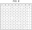
- FIG. 8 is a diagram showing the truth table of the combinational circuit 148 that is a logic circuit based on a combination of multiple bits.
- D0 to D7 respectively represent bit values of 8-bit designation data.
- D0 represents the lowest bit value
- D7 represents the highest bit value.
- OUT represents a bit value output from the combinational circuit 148.
- Each bit value is represented by 0 or 1.
- "X" indicates that the bit value may be 0 or 1.
- the register value indicating the invalidation of the thermal shutdown function is "11101010".
- a second row indicates that the bit values of the 8-bit designation data respectively match bit values of the register value "11101010", and in this case, the combinational circuit 148 outputs 1-bit designation data "0" indicating the invalidation of the thermal shutdown function.
- third and subsequent rows indicate that any of the bit values of the 8-bit designation data does not match bit values of the register value "11101010", and in this case, the combinational circuit 148 outputs 1-bit designation data "1" indicating the validation of the thermal shutdown function.
- the combinational circuit 148 outputs the 1-bit designation data "0" indicating the invalidation of the thermal shutdown function only when the bit values of the 8-bit designation data DTS [7, 0] designating the validation or invalidation of the thermal shutdown function output from the setting data register 122 completely match the bit values of the register value "11101010” designating the invalidation of the thermal shutdown function, and otherwise outputs the 1-bit designation data "1" indicating the validation of the thermal shutdown function.
- the combinational circuit 148 outputs the 1-bit designation data "0" or "1" to the AND circuit 145.
- the AND circuit 145 that receives output of the combinational circuit 148 has the same function as the AND circuit 145 in the head drive circuit 101 according to the related-art example.
- the AND circuit 145 outputs "0" when both the received data from the temperature sensor unit 140 and the received data from the combinational circuit 148 are not "1". That is, the AND circuit 145 outputs "0" when the head drive circuit 101 is not in the abnormal heat generation state or the thermal shutdown function is set to be invalidated even though the head drive circuit 101 is in an abnormal heat generation state.
- the output data "0" from the AND circuit 145 is data instructing continuation of driving of the logic unit 120 and the analog unit 130 of the head drive circuit 101.
- the AND circuit 145 outputs "1" when both the received data from the temperature sensor unit 140 and the received data from the combinational circuit 148 are “1". That is, the AND circuit 145 outputs "1" only when the head drive circuit 101 is in the abnormal heat generation state and the thermal shutdown function is set to be validated.
- the output data "1" from the AND circuit 145 is data instructing stop of driving of the logic unit 120 and the analog unit 130 of the head drive circuit 101.
- the decoder state machine 172 outputs data designating a waveform output level to the waveform level selector 173 and the waveform level selector 174 based on the pulse signal generated by the waveform timer 171.
- FW [4:0] indicates 5-bit data corresponding to the power supply levels VSS, VA, VB, VC, and VD shown in FIG. 9 .
- FIG. 11 is a diagram showing a list of a waveform output level of a drive waveform output from the gate driver 133, an ON switch, and an ON resistance.
- the ON switch means a switch element that is turned on to obtain a desired waveform output level
- the ON resistance means a resistance while the switch element is turned on.
- the ON resistance of each of the switch elements QS, QA, QB, QC, and QD is 200 ⁇ . If the power supply levels VB, VC, and VD are the same, it is permitted to simultaneously turn on the switch elements QB, QC, and QD. In this case, the combined ON resistance (parallel resistance) of the switch elements QB, QC, and QD is 66.7 ⁇ .
- a magnitude of the ON resistance is related to a speed at which the drive waveform for driving the actuator PZT rises and falls.
- the drive waveform rises and falls faster when the ON resistance (parallel resistance) is low than when the ON resistance (parallel resistance) is high.
- the decoder state machine 172 determines whether to allow simultaneous turning-on of the plurality of switch elements connected in parallel based on power supply level data in the setting data and the designation data DSP designating the validation or invalidation of the short-circuit prevention function, and then determines the waveform pattern to be output from the waveform level selectors 173 and 174. That is, the decoder state machine 172 includes the short-circuit prevention circuit 125 (see FIG. 2 ), and validates or invalidates the short-circuit prevention function.
- the program according to the present embodiment may be transferred while being stored in an electronic device, or may be transferred without being stored in an electronic device. In the latter case, the program may be transferred via a network or may be transferred while being stored in a storage medium.
- the storage medium is a non-transitory tangible medium.
- the storage medium is a computer-readable medium.
- the storage medium may be of any type as long as the storage medium can store a program and is readable by a computer, such as a CD-ROM or a memory card.
Landscapes
- Accessory Devices And Overall Control Thereof (AREA)
- Ink Jet (AREA)
- Particle Formation And Scattering Control In Inkjet Printers (AREA)
Abstract
Description
- Embodiments described herein relate generally to an ink jet head drive circuit.
- Generally, an inkjet head includes a pressure chamber that accommodates ink, an actuator that expands and contracts the pressure chamber, and an ink jet head drive circuit that drives the actuator. The ink jet head drive circuit ejects ink from a nozzle communicating with the pressure chamber by expanding and contracting the pressure chamber by the actuator.
- Generally, an ink jet head drive circuit has protection functions such as a thermal shutdown function for preventing abnormal heat generation and a short-circuit prevention function for preventing a short-circuit due to switch elements having different power supply levels being simultaneously turned on.
- However, it may be desired to invalidate the protection function. For example, there are cases where it is desired to perform an operation test in a high temperature environment or at a high temperature at the time of overload, and where it is desired to drive the switch elements by simultaneously turning on the switch elements with different power supply levels set to the same potential.
- The protection function is invalidated by setting data. However, the protection function may be unintentionally invalidated due to erroneous setting or a bit error. It is desirable to prevent unintentional invalidation of the protection function as much as possible.
- To this end, there is provided an inkjet head drive circuit according to
claim 1. Preferred embodiments are set out in the dependent claims. There is also provided an ink jet head according to claim 15. -
-
FIG. 1 is a block diagram showing a configuration example of an inkjet printer including an inkjet head drive circuit according to an embodiment; -
FIG. 2 is a block diagram showing a configuration example of an ink jet head drive circuit according to a related-art example; -
FIG. 3 is a diagram showing an example of a register map of setting data related to validation and invalidation of a protection function; -
FIG. 4 is a diagram showing specific register values indicating the validation and invalidation; -
FIG. 5 is a block diagram showing a configuration example of the inkjet head drive circuit according to the embodiment; -
FIG. 6 is a diagram showing an example of a register map of setting data related to validation and invalidation of a protection function; -
FIG. 7 is a diagram showing specific register values indicating the validation and invalidation; -
FIG. 8 is a diagram showing a truth table of a logic circuit based on combinations of multiple bits; -
FIG. 9 is a block diagram showing a configuration example of a gate driver; -
FIG. 10 is a block diagram showing a configuration example of a waveform pattern generation unit; and -
FIG. 11 is a diagram showing an example of an ON switch that is enabled by invalidating a short-circuit prevention function. - In general, according to one embodiment, an ink jet head drive circuit that prevents unintentional invalidation of a protection function is provided.
- According to one embodiment, an ink jet head drive circuit includes a drive unit configured to drive an actuator that expands and contracts a pressure chamber accommodating ink to eject the ink from a nozzle, a protection circuit configured to execute a protection function of the inkjet head drive circuit, and a setting data register configured to store setting data including multi-bit designation data designating validation or invalidation of the protection function and to output the multi-bit designation data to the protection circuit. The protection circuit invalidates the protection function only when bit values of the multi-bit designation data match bit values of multi-bit invalidation designation data designating the invalidation of the protection function. The protection circuit validates the protection function when the bit values of the multi-bit designation data do not match the bit values of the multi-bit invalidation designation data.
- First, an
inkjet printer 200 having aninkjet head 100 including an inkjethead drive circuit 101 according to an embodiment will be described with reference toFIG. 1. FIG. 1 is a block diagram showing a configuration example of theink jet printer 200. In the following description, theinkjet printer 200 is abbreviated as aprinter 200, theink jet head 100 is abbreviated as ahead 100, and the ink jethead drive circuit 101 is abbreviated as ahead drive circuit 101. - The
printer 200 includes thehead 100. Thehead 100 includes thehead drive circuit 101 and anactuator group 102. Theactuator group 102 includes a plurality of actuators. Each actuator is a drive element for expanding and contracting a pressure chamber that accommodates ink and ejecting ink droplets from a nozzle communicating with the pressure chamber. For example, the actuator is a piezoelectric drive element made of lead zirconate titanate (PZT). Thehead drive circuit 101 generates a drive signal for theactuator group 102. The actuator in theactuator group 102 operates according to the drive signal supplied from thehead drive circuit 101, expands and contracts the pressure chamber, and ejects the ink droplets from the nozzle. - The
printer 200 includes, in addition to thehead 100, aprocessor 201, a read only memory (ROM) 202, a random access memory (RAM) 203, anoperation panel 204, acommunication interface 205, aconveyance motor 206, amotor drive circuit 207, apump 208, and apump drive circuit 209. In the drawings, the interface is abbreviated as "IF". - The
printer 200 also includes abus line 210 such as an address bus or a data bus. Theprocessor 201, theROM 202, theRAM 203, theoperation panel 204, thecommunication interface 205, themotor drive circuit 207, thepump drive circuit 209, and thehead drive circuit 101 are connected to thebus line 210 directly or via an input and output circuit, and can transmit data to and receive data from each other. - The
processor 201 corresponds to a central part of a computer. Theprocessor 201 controls the units to implement various functions of theprinter 200 according to an operating system and application programs. Theprocessor 201 is, for example, a central processing unit (CPU). - The
ROM 202 corresponds to a read-only main storage portion of the computer. TheROM 202 stores the operating system and the application programs. TheROM 202 may store data necessary for theprocessor 201 to execute processing for controlling the units. - The
RAM 203 corresponds to a rewritable main storage portion of the computer. TheRAM 203 stores data necessary for theprocessor 201 to execute processing. TheRAM 203 is also used as a work area where information is appropriately rewritten by theprocessor 201. The work area includes an image memory in which print data is loaded. - The
operation panel 204 includes an operation unit and a display unit. The operation unit includes function keys such as a power key, a paper feed key, and an error release key arranged thereon. The display unit can display various states of theprinter 200. - The
communication interface 205 receives print data from a client terminal connected via a network such as a local area network (LAN). For example, when an error occurs in theprinter 200, thecommunication interface 205 transmits a signal notifying the client terminal of the error. - The
motor drive circuit 207 controls driving of theconveyance motor 206. Theconveyance motor 206 functions as a drive source of a conveyance mechanism that conveys a recording medium such as printing paper. When theconveyance motor 206 is started, the conveyance mechanism starts conveying the recording medium. The conveyance mechanism conveys the recording medium to a printing position of thehead 100. The conveyance mechanism discharges the printed recording medium from a discharge port (not shown) to the outside of theprinter 200. - The
pump drive circuit 209 controls driving of thepump 208. When thepump 208 is driven, ink in an ink tank (not shown) is supplied to thehead 100. - The
head drive circuit 101 drives theactuator group 102 of thehead 100 based on the print data. Theactuator group 102 expands and contracts the pressure chamber that accommodates the ink, and ejects the ink droplets from the nozzle communicating with the pressure chamber. Accordingly, thehead 100 ejects the ink onto the recording medium conveyed by the conveyance mechanism, and prints an image or the like on the recording medium. - Next, the
head drive circuit 101 according to a related-art example will be described with reference toFIG. 2. FIG. 2 is a block diagram showing a configuration example of thehead drive circuit 101 according to the related-art example. - The
head drive circuit 101 includes an I/O unit 110, alogic unit 120, and ananalog unit 130. The I/O unit 110, thelogic unit 120, and theanalog unit 130 are drive units that drive theactuator group 102. - The I/
O unit 110 includes acomparator 111 and a serial-parallel conversion unit 112. In the drawings, the "serial-parallel conversion unit" is abbreviated as a "conversion unit". - The
comparator 111 receives a clock signal CLK of low voltage differential signaling (LVDS) and a data signal DI. The data signal DI includes print data, setting data, and the like. Thecomparator 111 outputs data of the clock signal CLK and data of the data signal DI to the serial-parallel conversion unit 112. - The serial-
parallel conversion unit 112 converts serial format data received from thecomparator 111 into parallel format data. The data of the data signal DI is acquired at a timing when the clock signal CLK rises. Specifically, at a timing when the clock signal CLK changes from 0 to 1, values (0 or 1) of setting data and the print data included in the data signal DI are acquired. The serial-parallel conversion unit 112 outputs the data of the parallel format data signal DI to thelogic unit 120. The serial-parallel conversion unit 112 outputs the data of the clock signal CLK to thelogic unit 120 and the analog unit. - The
logic unit 120 includes a startbyte recognition unit 121, a settingdata register 122, aprint data register 123, and a waveformpattern generation unit 124. - The start
byte recognition unit 121 recognizes a start byte for the data of the parallel format data signal DI received from the serial-parallel conversion unit 112, and separates the data into setting data and print data. The startbyte recognition unit 121 outputs the setting data to the settingdata register 122 and outputs the print data to the print data register 123. - The setting
data register 122 stores the setting data received from the startbyte recognition unit 121. - The print data register 123 stores the print data received from the start
byte recognition unit 121. - The waveform
pattern generation unit 124 acquires setting data from the settingdata register 122, acquires print data from the print data register 123, and generates a waveform pattern based on the setting data and the print data. The waveformpattern generation unit 124 outputs the generated waveform pattern to theanalog unit 130. - The
analog unit 130 includes alevel shifter 131, a pre-buffer 132, and agate driver 133. - The
level shifter 131 converts the waveform pattern received from the waveformpattern generation unit 124 into a high voltage. Thelevel shifter 131 outputs the waveform pattern converted into the high voltage to the pre-buffer 132. - The pre-buffer 132 appropriately amplifies and shapes the waveform pattern received from the
level shifter 131. The pre-buffer 132 outputs the appropriately amplified and shaped waveform pattern to thegate driver 133. - The
gate driver 133 outputs a drive waveform for driving theactuator group 102 of thehead 100 to an output electrode OUT connected to theactuator group 102 by controlling on and off of a plurality of switch elements of thegate driver 133 based on the waveform pattern received from the pre-buffer 132. That is, thegate driver 133 is a drive waveform output unit that outputs the drive waveform based on the waveform pattern. For example, the switch element is a MOSFET, and thegate driver 133 controls on and off of the MOSFET by applying a control signal (gate voltage) to a gate of the MOSFET. - The
head drive circuit 101 also has a thermal shutdown function and a short-circuit prevention function as protection functions. The thermal shutdown function is a function for preventing abnormal heat generation of thehead drive circuit 101. The short-circuit prevention function is a function for preventing occurrence of a short-circuit in thegate driver 133 due to a plurality of switch elements having different power supply levels being simultaneously turned on. - It may be desired to invalidate the thermal shutdown function and the short-circuit prevention function. For example, there are cases where it is desired to perform an operation test in a high temperature environment or at a high temperature at the time of overload, and where it is desired to drive the switch elements by simultaneously turning on the switch elements with different power supply levels set to the same potential.
- Validation and invalidation of the thermal shutdown function and the short-circuit prevention function can be switched by the setting data stored in the setting
data register 122. In other words, the setting data stored in the settingdata register 122 includes designation data designating the validation and invalidation of the thermal shutdown function and the short-circuit prevention function. - The
head drive circuit 101 includes atemperature sensor unit 140 as a protection circuit for executing the thermal shutdown function. Thetemperature sensor unit 140 includes atemperature sensor 141, areference power supply 142, and acomparator 143. Thetemperature sensor 141 detects a temperature of thehead drive circuit 101 and outputs a voltage signal indicating the temperature. Thereference power supply 142 provides a reference voltage as a threshold for determining abnormal heat generation. Thecomparator 143 compares the voltage signal output from thetemperature sensor 141 with the reference voltage. - The
comparator 143 outputs binary data TS indicating whether thehead drive circuit 101 is in an abnormal heat generation state depending on a comparison result. For example, when the temperature is equal to or higher than the threshold, thecomparator 143 outputs the binary data TS "1" indicating that thehead drive circuit 101 is in the abnormal heat generation state. The binary data TS "1" is control data instructing execution of the thermal shutdown function. On the other hand, when the temperature is lower than the threshold, the binary data TS "0" indicating that thehead drive circuit 101 is not in the abnormal heat generation state is output. The binary data TS "0" is control data not instructing execution of the thermal shutdown function. - Validation and invalidation of the thermal shutdown function can be set by the designation data in the setting data stored in the setting
data register 122. The settingdata register 122 outputs designation data DTS designating the validation or invalidation of the thermal shutdown function. -
FIG. 3 shows an example of a register map of the designation data designating the validation and invalidation of the thermal shutdown function and the short-circuit prevention function. InFIG. 3 , thermal shutdown is abbreviated as shutdown. The same applies toFIGS. 4 ,7 , and8 . The settingdata register 122 stores, at a predetermined address, name information indicating the thermal shutdown function and the designation data DTS associated with the name information and designating the validation or invalidation of the thermal shutdown function. The settingdata register 122 stores the setting data as 8-bit (D0 to D7) data. The settingdata register 122 stores the designation data DTS designating the validation or invalidation of the thermal shutdown function as lowest 1-bit (D0) data. -
FIG. 4 is a diagram showing specific register values indicating the validation and invalidation of the thermal shutdown function and the short-circuit prevention function in the register map of the designation data shown inFIG. 3 . The register value indicating the validation of the thermal shutdown function is "00000001". The register value indicating the invalidation of the thermal shutdown function is "00000000". - In the setting for validating the thermal shutdown function, the setting
data register 122 outputs lowest 1-bit (D0) binary data, that is, "1". On the other hand, in the setting for invalidating the thermal shutdown function, the settingdata register 122 outputs lowest 1-bit (D0) binary data, that is, "0". - Referring again to
FIG. 2 , thehead drive circuit 101 will be described. Thehead drive circuit 101 also includes an ANDcircuit 145 that receives output of thetemperature sensor unit 140 and output of the settingdata register 122. The ANDcircuit 145 receives, from the settingdata register 122, binary data " 1" or "0" indicating that the thermal shutdown function is to be validated or invalidated. - The AND
circuit 145 outputs "0" when both the received data from thetemperature sensor unit 140 and the received data from the settingdata register 122 are not " 1". That is, the ANDcircuit 145 outputs "0" when thehead drive circuit 101 is not in the abnormal heat generation state or the thermal shutdown function is set to be invalidated even though thehead drive circuit 101 is in an abnormal heat generation state. The output data "0" from the ANDcircuit 145 is data instructing continuation of driving of thelogic unit 120 and theanalog unit 130 of thehead drive circuit 101. - On the other hand, the AND
circuit 145 outputs "1" when both the received data from thetemperature sensor unit 140 and the received data from the settingdata register 122 are "1". That is, the ANDcircuit 145 outputs "1" only when thehead drive circuit 101 is in the abnormal heat generation state and the thermal shutdown function is set to be validated. The output data "1" from the ANDcircuit 145 is data instructing stop of driving of thelogic unit 120 and theanalog unit 130 of thehead drive circuit 101. - The
head drive circuit 101 can receive a reset signal for forcibly stopping thelogic unit 120 and theanalog unit 130. The reset signal is input to thelogic unit 120 and theanalog unit 130. Thelogic unit 120 and theanalog unit 130 stop when receiving the reset signal. For example, the reset signal is binary data " 1". The driving of thelogic unit 120 and theanalog unit 130 may be stopped by any method such as stopping reception processing of the print data and stopping output of the gate driver. - The
head drive circuit 101 also includes an ORcircuit 146 that receives the reset signal and output of the ANDcircuit 145. The ORcircuit 146 outputs "1" when one of the output of the ANDcircuit 145 and the reset signal is "1". That is, the output data "1" from theOR circuit 146 is data instructing stop of driving of thelogic unit 120 and theanalog unit 130 of thehead drive circuit 101. - The
head drive circuit 101 includes a short-circuit prevention circuit 125 in the waveformpattern generation unit 124 as a protection circuit for executing the short-circuit prevention function. The short-circuit prevention circuit 125 is a circuit that prevents the waveformpattern generation unit 124 from generating a waveform pattern in which switch elements of different power supply levels of thegate driver 133 are simultaneously turned on. - Validation and invalidation of the short-circuit prevention function can be designated by the designation data stored in the setting
data register 122. The settingdata register 122 outputs designation data DSP designating the validation or invalidation of the short-circuit prevention function to the waveformpattern generation unit 124. The waveformpattern generation unit 124 validates or invalidates the short-circuit prevention circuit 125 according to the designation data DSP. - Next, the validation and invalidation of the short-circuit prevention function will be described with reference to
FIG. 3 . As described above,FIG. 3 is a diagram showing the example of the register map of the data designating the validation and invalidation of the thermal shutdown function and the short-circuit prevention function. - Similarly to the thermal shutdown function, the setting
data register 122 stores, at a predetermined address, name information indicating the short-circuit prevention function and the data DSP associated with the name information and indicating the validation or invalidation of the short-circuit prevention function. The settingdata register 122 stores the setting data as 8-bit (D0 to D7) data. The settingdata register 122 stores the designation data DSP designating the validation or invalidation of the short-circuit prevention function as lowest 1-bit (D0) data. - As shown in
FIG. 4 , similarly to the thermal shutdown function, the register value indicating the validation of the short-circuit prevention function is "00000001". The register value indicating the invalidation of the short-circuit prevention function is "00000000". - In the setting for validating the short-circuit prevention function, the setting
data register 122 outputs, to the waveformpattern generation unit 124, lowest 1-bit (D0) binary data, that is, "1". The output data "1" from the settingdata register 122 is data validating the short-circuit prevention circuit 125. In this case, the waveformpattern generation unit 124 generates a waveform pattern to be output to theanalog unit 130 using the short-circuit prevention circuit 125. - On the other hand, in the setting for invalidating the short-circuit prevention function, the setting
data register 122 outputs, to the waveformpattern generation unit 124, lowest 1-bit (D0) binary data, that is, "0". The output data "0" from the settingdata register 122 is data invalidating the short-circuit prevention circuit 125. In this case, the waveformpattern generation unit 124 generates a waveform pattern to be output to theanalog unit 130 without using the short-circuit prevention circuit 125. - In the
head drive circuit 101 according to the related-art example described above, designation data designating validation and invalidation of protection functions (that is, the thermal shutdown function and the short-circuit prevention function) is 1-bit data stored in the settingdata register 122. When the designation data is 1-bit data, the protection function may be unintentionally invalidated due to an erroneous operation at the time of inputting setting data, a bit error during data processing, or the like. Since unintentional invalidation of the protection function causes a malfunction, it is desirable to avoid this as much as possible. - The
head drive circuit 101 according to the embodiment prevents occurrence of unintentional invalidation of the protection functions related to the designation data designating the validation and invalidation of the protection functions (that is, the thermal shutdown function and the short-circuit prevention function). - Hereinafter, the
head drive circuit 101 according to the embodiment will be described with reference toFIG. 5. FIG. 5 is a block diagram showing a configuration example of thehead drive circuit 101 according to the embodiment. InFIG. 5 , members denoted by the same reference numerals as those shown inFIG. 2 are the same members, and detailed description thereof will be omitted. Hereinafter, differences will be mainly described. - In the
head drive circuit 101 according to the embodiment, the settingdata register 122 stores designation data designating validation and invalidation of protection functions (that is, a thermal shutdown function and a short-circuit prevention function) as multi-bit data. That is, the settingdata register 122 outputs multi-bit designation data as the designation data designating the validation and invalidation of the protection functions (that is, the thermal shutdown function and the short-circuit prevention function). - For example, the setting
data register 122 outputs 8-bit designation data DTS [7, 0] as designation data designating validation or invalidation of the thermal shutdown function. The settingdata register 122 outputs 8-bit designation data DSP [7, 0] as designation data designating validation or invalidation of the short-circuit prevention function. - The
head drive circuit 101 according to the embodiment includes alogic circuit 148 based on a combination of multiple bits and alogic circuit 126 based on a combination of multiple bits in order to generate 1-bit designation data from multi-bit designation data. Hereinafter, the logic circuit based on the combination of multiple bits is abbreviated as a combinational circuit. - The
combinational circuit 148 generates 1-bit designation data to be input to the ANDcircuit 145 from the 8-bit designation data DTS [7, 0] designating the validation or invalidation of the thermal shutdown function output from the settingdata register 122. Thecombinational circuit 148 constitutes a part of a protection circuit for executing the thermal shutdown function. In other words, thehead drive circuit 101 according to the embodiment includes thetemperature sensor unit 140 and thecombinational circuit 148 as the protection circuit for executing the thermal shutdown function. Thecombinational circuit 148 prevents occurrence of unintentional invalidation of the thermal shutdown function. - The
combinational circuit 126 generates 1-bit designation data to be input to the waveformpattern generation unit 124 from the 8-bit designation data DSP [7, 0] designating the validation or invalidation of the short-circuit prevention function output from the settingdata register 122. Thecombinational circuit 126 constitutes a part of a protection circuit for executing the short-circuit prevention function. Thehead drive circuit 101 according to the embodiment includes the short-circuit prevention circuit 125 and thecombinational circuit 126 as the protection circuit for executing the short-circuit prevention function. Thecombinational circuit 126 prevents occurrence of unintentional invalidation of the short-circuit prevention function. -
FIG. 6 shows an example of a register map of data designating the validation and invalidation of the thermal shutdown function and the short-circuit prevention function stored in the settingdata register 122, in thehead drive circuit 101 according to the embodiment. - The setting
data register 122 stores, at a predetermined address, name information indicating the thermal shutdown function and the 8-bit designation data DTS [7, 0] associated with the name information and designating the validation or invalidation of the thermal shutdown function. Similarly, the settingdata register 122 stores, at a predetermined address, name information indicating the short-circuit prevention function and the 8-bit designation data DSP [7, 0] associated with the name information and designating the validation or invalidation of the short-circuit prevention function. As described above, the settingdata register 122 stores setting data as 8-bit (D0 to D7) data. - In the
head drive circuit 101 according to the related-art example, the lowest 1 bit (D0) in the 8-bit (D0 to D7) setting data stored in the settingdata register 122 is allocated to the designation data DTS designating the validation or invalidation of the thermal shutdown function. The same applies to the designation data DSP designating the validation or invalidation of the short-circuit prevention function. - In contrast, in the
head drive circuit 101 according to the embodiment, all bits in the 8-bit (D0 to D7) setting data stored in the settingdata register 122 are allocated to the designation data DTS [7, 0] designating the validation or invalidation of the thermal shutdown function. The same applies to the designation data DSP [7, 0] designating the validation or invalidation of the short-circuit prevention function. -
FIG. 7 is a diagram showing specific register values indicating the validation and invalidation of the thermal shutdown function and the short-circuit prevention function in the register map of the designation data shown inFIG. 6 . The register value indicating the invalidation of the thermal shutdown function is "11101010". The register value "XXXXXXXX" indicating the validation of the thermal shutdown function is a value different from "11101010". The register value indicating the invalidation of the short-circuit prevention function is "11011010". The register value "XXXXXXXX" indicating the validation of the short-circuit prevention function is a value different from "11011010". - Next, a truth table of the
combinational circuit 148 will be described with reference toFIG. 8. FIG. 8 is a diagram showing the truth table of thecombinational circuit 148 that is a logic circuit based on a combination of multiple bits. InFIG. 8 , D0 to D7 respectively represent bit values of 8-bit designation data. D0 represents the lowest bit value, and D7 represents the highest bit value. OUT represents a bit value output from thecombinational circuit 148. Each bit value is represented by 0 or 1. "X" indicates that the bit value may be 0 or 1. - As shown in
FIG. 7 , the register value indicating the invalidation of the thermal shutdown function is "11101010". InFIG. 8 , a second row indicates that the bit values of the 8-bit designation data respectively match bit values of the register value "11101010", and in this case, thecombinational circuit 148 outputs 1-bit designation data "0" indicating the invalidation of the thermal shutdown function. - In
FIG. 8 , third and subsequent rows indicate that any of the bit values of the 8-bit designation data does not match bit values of the register value "11101010", and in this case, thecombinational circuit 148 outputs 1-bit designation data "1" indicating the validation of the thermal shutdown function. - That is, the
combinational circuit 148 outputs the 1-bit designation data "0" indicating the invalidation of the thermal shutdown function only when the bit values of the 8-bit designation data DTS [7, 0] designating the validation or invalidation of the thermal shutdown function output from the settingdata register 122 completely match the bit values of the register value "11101010" designating the invalidation of the thermal shutdown function, and otherwise outputs the 1-bit designation data "1" indicating the validation of the thermal shutdown function. - The
combinational circuit 148 outputs the 1-bit designation data "0" or "1" to the ANDcircuit 145. The ANDcircuit 145 that receives output of thecombinational circuit 148 has the same function as the ANDcircuit 145 in thehead drive circuit 101 according to the related-art example. - That is, the AND
circuit 145 outputs "0" when both the received data from thetemperature sensor unit 140 and the received data from thecombinational circuit 148 are not "1". That is, the ANDcircuit 145 outputs "0" when thehead drive circuit 101 is not in the abnormal heat generation state or the thermal shutdown function is set to be invalidated even though thehead drive circuit 101 is in an abnormal heat generation state. The output data "0" from the ANDcircuit 145 is data instructing continuation of driving of thelogic unit 120 and theanalog unit 130 of thehead drive circuit 101. - On the other hand, the AND
circuit 145 outputs "1" when both the received data from thetemperature sensor unit 140 and the received data from thecombinational circuit 148 are "1". That is, the ANDcircuit 145 outputs "1" only when thehead drive circuit 101 is in the abnormal heat generation state and the thermal shutdown function is set to be validated. The output data "1" from the ANDcircuit 145 is data instructing stop of driving of thelogic unit 120 and theanalog unit 130 of thehead drive circuit 101. - The OR
circuit 146 that receives output of the ANDcircuit 145 also has the same function as theOR circuit 146 in thehead drive circuit 101 according to the related-art example. - The
combinational circuit 126 has the same function as thecombinational circuit 148. That is, thecombinational circuit 126 outputs the 1-bit designation data "0" indicating the invalidation of the short-circuit prevention function only when the bit values of the 8-bit designation data DTS [7, 0] designating the validation or invalidation of the short-circuit prevention function output from the settingdata register 122 completely match the bit values of the register value "11011010" designating the invalidation of the short-circuit prevention function, and otherwise outputs the 1-bit designation data "1" indicating the validation of the short-circuit prevention function. - As described above, in the
head drive circuit 101 according to the embodiment, all bits in the 8-bit setting data stored in the settingdata register 122 are allocated to the designation data designating the validation or invalidation of the protection function. For this reason, even when an erroneous operation at the time of inputting setting data, a bit error during data processing, or the like occurs, it is unlikely that all the bit values of the designation data completely match the register value designating the invalidation of the protection function. It can be considered that such a situation does notoccur at all. Therefore, in thehead drive circuit 101 according to the embodiment, it is considered that occurrence of unintentional invalidation of the protection function is prevented. - Hereinafter, the short-circuit prevention function will be described with reference to
FIGS. 9 to 11 . Hereinafter, first, a configuration example of thegate driver 133 provided in theanalog unit 130 of thehead drive circuit 101 will be described, then a configuration example of the waveformpattern generation unit 124 provided in thelogic unit 120 of thehead drive circuit 101 will be described, and then an operation example of thegate driver 133 and the waveformpattern generation unit 124 in which the short-circuit prevention function is validated and invalidated will be described. - First, the
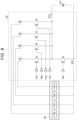
gate driver 133 will be described with reference toFIG. 9. FIG. 9 is a block diagram showing a configuration example of thegate driver 133. Thegate driver 133 shown inFIG. 9 corresponds to one actuator PZT in theactuator group 102. - The
gate driver 133 includes a plurality of switch elements QS, QA, QB, QC, and QD. The switch elements QS, QA, QB, QC, and QD are provided with appropriate power supply levels by a drive power supply PS. - For example, the drive power supply PS includes a plurality of power supplies PSA, PSB, PSC, and PSD. The power supply PSA provides the switch element QA with a power supply level VA with respect to a reference potential VSS. The power supply PSB provides the switch element QB with a power supply level VB with respect to the reference potential VSS. The power supply PSC provides the switch element QC with a power supply level VC with respect to the reference potential VSS. The power supply PSD provides the switch element QD with a power supply level VD with respect to the reference potential VSS. For example, the reference potential VSS is a negative potential, and the power supply levels VA, VB, VC, and VD are positive potentials.
- The switch element QS connects a pair of electrodes of the actuator PZT. The switch elements QA, QB, QC, and QD connect the actuator PZT and the power supplies PSA, PSB, PSC, and PSD, respectively. Specifically, the switch element QA connects the other electrode of the actuator PZT and the other power supply terminal of the power supply PSA. The switch element QB connects the other electrode of the actuator PZT and the other power supply terminal of the power supply PSB. The switch element QC connects the other electrode of the actuator PZT and the other power supply terminal of the power supply PSC. The switch element QD connects the other electrode of the actuator PZT and the other power supply terminal of the power supply PSD.
- For example, the switch elements QS and QA to QD are MOSFETs. The switch element QS is turned on by a gate voltage NSg, and an output level at that time is VSS. The switch element QAis turned on by a gate voltage PAg, and an output level at that time is VA. The switch element QB is turned on by a gate voltage PBg, and an output level at that time is VB. The switch element QC is turned on by a gate voltage PCg, and an output level at that time is VC. The switch element QD is turned on by a gate voltage PDg, and an output level at that time is VD.
- Next, the waveform
pattern generation unit 124 will be described with reference toFIG. 10. FIG. 10 is a block diagram showing a configuration example of the waveformpattern generation unit 124. - The waveform
pattern generation unit 124 includes awaveform timer 171, adecoder state machine 172, awaveform level selector 173, and awaveform level selector 174. - The
waveform timer 171 is a timer circuit that generates a pulse signal for forming ink drops in a multi-drop method. Fire1, Fire2, ..., and Fire14 respectively correspond to the ink drops (gradations). Timer [7:0] indicates that the pulse signal is 8-bit data. - The
decoder state machine 172 outputs data designating a waveform output level to thewaveform level selector 173 and thewaveform level selector 174 based on the pulse signal generated by thewaveform timer 171. FW [4:0] indicates 5-bit data corresponding to the power supply levels VSS, VA, VB, VC, and VD shown inFIG. 9 . - The
waveform level selectors waveform level selectors waveform level selectors gate driver 133, signals (gate voltages) NSg, PAg, PBg, PCg, and PDg for turning on the switch elements QS, QA, QB, QC, and QD based on the print data. - The waveform
pattern generation unit 124 controls on and off of the switch elements QS, QA, QB, QC and QD in thegate driver 133 based on the print data and the setting data. Accordingly, thegate driver 133 outputs a drive waveform for driving the one actuator PZT in theactuator group 102 of thehead 100. - In the
gate driver 133 shown inFIG. 9 , it is not permitted to simultaneously turn on a plurality of switch elements connected in series, specifically, the switch element QS and any of the switch elements QA, QB, QC, QD. - The power supply levels VA, VB, VC, and VD of the switch elements QA, QB, QC, and QD are generally different. In this case, it is not permitted to simultaneously turn on two or more of the switch elements QA, QB, QC, QD connected in parallel.
- However, it is permitted to simultaneously turn on the switch elements QA, QB, QC, QD of the same power supply levels VA, VB, VC, VD.
-
FIG. 11 is a diagram showing a list of a waveform output level of a drive waveform output from thegate driver 133, an ON switch, and an ON resistance. The ON switch means a switch element that is turned on to obtain a desired waveform output level, and the ON resistance means a resistance while the switch element is turned on. - As shown in
FIG. 11 , the ON resistance of each of the switch elements QS, QA, QB, QC, and QD is 200 Ω. If the power supply levels VB, VC, and VD are the same, it is permitted to simultaneously turn on the switch elements QB, QC, and QD. In this case, the combined ON resistance (parallel resistance) of the switch elements QB, QC, and QD is 66.7 Ω. - A magnitude of the ON resistance (parallel resistance) is related to a speed at which the drive waveform for driving the actuator PZT rises and falls. The drive waveform rises and falls faster when the ON resistance (parallel resistance) is low than when the ON resistance (parallel resistance) is high.
- Therefore, for the plurality of switch elements connected in parallel and having the same power supply level, by invalidating the short-circuit prevention function and simultaneously turning on the switch elements, it is also possible to perform control such as speeding up rising and falling of the drive waveform of the actuator PZT.
- Therefore, the decoder state machine 172 (see
FIG. 10 ) determines whether to allow simultaneous turning-on of the plurality of switch elements connected in parallel based on power supply level data in the setting data and the designation data DSP designating the validation or invalidation of the short-circuit prevention function, and then determines the waveform pattern to be output from thewaveform level selectors decoder state machine 172 includes the short-circuit prevention circuit 125 (seeFIG. 2 ), and validates or invalidates the short-circuit prevention function. - The program according to the present embodiment may be transferred while being stored in an electronic device, or may be transferred without being stored in an electronic device. In the latter case, the program may be transferred via a network or may be transferred while being stored in a storage medium. The storage medium is a non-transitory tangible medium. The storage medium is a computer-readable medium. The storage medium may be of any type as long as the storage medium can store a program and is readable by a computer, such as a CD-ROM or a memory card.
- While certain embodiments have been described, these embodiments have been presented by way of example only, and are not intended to limit the scope of the exemplary embodiments. The novel embodiments can be implemented in various other forms, and various omissions, substitutions, and changes can be made in a scope not departing from the exemplary embodiments. The embodiments and the modifications thereof are included in the scope of the exemplary embodiments, and are included in a scope of the exemplary embodiments disclosed in the claims.
Claims (15)
- An ink jet head drive circuit (101) that drives an ink jet head, the ink jet head including a pressure chamber configured to accommodate ink, a nozzle configured to communicate with the pressure chamber, and an actuator configured to expand and contract the pressure chamber to eject the ink from the nozzle, the circuit comprising:a drive unit configured to drive the actuator;a protection circuit configured to execute a protection function of the ink jet head drive circuit; anda setting data register (122) configured to store setting data including multi-bit designation data designating validation or invalidation of the protection function and to output the multi-bit designation data to the protection circuit, whereinthe protection circuit invalidates the protection function only when bit values of the multi-bit designation data match bit values of multi-bit invalidation designation data designating the invalidation of the protection function, andthe protection circuit validates the protection function when the bit values of the multi-bit designation data do not match the bit values of the multi-bit invalidation designation data.
- The circuit according to claim 1, wherein
the protection circuit includes a logic circuit configured to generate 1-bit designation data from the multi-bit designation data. - The circuit according to claim 2, wherein
the logic circuit receives the bit values of the multi-bit designation data, and outputs "0" when the bit values of the multi-bit designation data match the bit values of the multi-bit invalidation designation data, and outputs "1" when the bit values of the multi-bit designation data do not match the bit values of the multi-bit invalidation designation data. - The circuit according to any one of claims 1 to 3, wherein all bits in the setting data stored in the setting data register are allocated to the designation data designating validation or invalidation of the protection function.
- The circuit according to any one of claims 1 to 4, wherein the protection function includes a thermal shutdown function and/or a short-circuit prevention function.
- The circuit according to any one of claims 1 to 5, further comprising:a temperature sensor (141) configured to detect a temperature of the inkjet head drive circuit; anda comparator (111) configured to compare the temperature detected by the temperature sensor with a threshold, whereinthe protection circuit stops the drive unit when the detected temperature is equal to or higher than the threshold.
- The circuit according to claim 6, wherein:the protection function includes a thermal shutdown function, andthe logic circuit comprises a first logic circuit (148) configured to generate 1-bit designation data from the multi-bit designation data designating the validation or invalidation of the thermal shutdown function.
- The circuit according to claim 7, further comprising an AND circuit (145) configured to receive the output of the first logic circuit.
- The circuit according to any one of claims 1 to 8, whereinthe drive unit includes a plurality of switch elements having different power supply levels, andthe protection circuit prevents the plurality of switch elements from being simultaneously turned on.
- The circuit according to any one of claims 1 to 9, whereinthe drive unit includes a plurality of switch elements having the same power supply level, andthe switch elements of the same power supply level are permitted to simultaneously turn on.
- The circuit according to claim 9 or 10, wherein the plurality of switch elements are connected in parallel.
- The circuit according to any one of claims 9 to 11, wherein:the protection function includes a short-circuit prevention function, andthe logic circuit comprises a second logic circuit (126) configured to generate 1-bit designation data from the multi-bit designation data designating the validation or invalidation of the short-circuit prevention function.
- The circuit according to claim 12, further comprising a waveform pattern generation unit configured to receive the output of the second logic circuit.
- The circuit according to claim 13, wherein the waveform pattern generation unit is configured to determine whether to allow simultaneous turning-on of the plurality of switch elements based on power supply level data in the setting data and the designation data, and to determine the waveform pattern to be output.
- An inkjet head (100) comprising:a pressure chamber configured to accommodate ink,a nozzle configured to communicate with the pressure chamber,an actuator configured to expand and contract the pressure chamber to eject the ink from the nozzle, andthe inkjet head drive circuit according to any one of claims 1 to 14.
Applications Claiming Priority (1)
| Application Number | Priority Date | Filing Date | Title |
|---|---|---|---|
| JP2023150445A JP2025043117A (en) | 2023-09-15 | 2023-09-15 | Inkjet head driver circuit |
Publications (2)
| Publication Number | Publication Date |
|---|---|
| EP4523914A1 true EP4523914A1 (en) | 2025-03-19 |
| EP4523914B1 EP4523914B1 (en) | 2026-06-17 |
Family
ID=91070293
Family Applications (1)
| Application Number | Title | Priority Date | Filing Date |
|---|---|---|---|
| EP24174998.5A Active EP4523914B1 (en) | 2023-09-15 | 2024-05-08 | Ink jet head drive circuit |
Country Status (2)
| Country | Link |
|---|---|
| EP (1) | EP4523914B1 (en) |
| JP (1) | JP2025043117A (en) |
Citations (3)
| Publication number | Priority date | Publication date | Assignee | Title |
|---|---|---|---|---|
| US6520615B1 (en) * | 1999-10-05 | 2003-02-18 | Hewlett-Packard Company | Thermal inkjet print head with integrated power supply fault protection circuitry for protection of firing circuitry |
| JP2016150567A (en) * | 2015-02-19 | 2016-08-22 | セイコーエプソン株式会社 | Liquid discharge device and liquid discharge method |
| WO2022066166A1 (en) * | 2020-09-25 | 2022-03-31 | Hewlett-Packard Development Company, L.P. | Fluidic dies including discharge circuits |
-
2023
- 2023-09-15 JP JP2023150445A patent/JP2025043117A/en active Pending
-
2024
- 2024-05-08 EP EP24174998.5A patent/EP4523914B1/en active Active
Patent Citations (3)
| Publication number | Priority date | Publication date | Assignee | Title |
|---|---|---|---|---|
| US6520615B1 (en) * | 1999-10-05 | 2003-02-18 | Hewlett-Packard Company | Thermal inkjet print head with integrated power supply fault protection circuitry for protection of firing circuitry |
| JP2016150567A (en) * | 2015-02-19 | 2016-08-22 | セイコーエプソン株式会社 | Liquid discharge device and liquid discharge method |
| WO2022066166A1 (en) * | 2020-09-25 | 2022-03-31 | Hewlett-Packard Development Company, L.P. | Fluidic dies including discharge circuits |
Also Published As
| Publication number | Publication date |
|---|---|
| JP2025043117A (en) | 2025-03-28 |
| EP4523914B1 (en) | 2026-06-17 |
Similar Documents
| Publication | Publication Date | Title |
|---|---|---|
| US10265950B2 (en) | Inkjet head control apparatus and inkjet printer | |
| EP1717041B1 (en) | Access to printing material container | |
| CN107825849B (en) | The ink ejecting method of ink-jet printer, ink gun and ink-jet printer | |
| US7036903B2 (en) | Inkjet printer checking nozzle and providing abnormal nozzle information and method thereof | |
| US6860577B2 (en) | Device for preventing printer header from overheating | |
| US9245210B2 (en) | Ink jet head and ink jet printing apparatus having the same | |
| US20090051957A1 (en) | Ink jet image forming apparatus and method of controlling the same | |
| JP4221953B2 (en) | Failure detection apparatus and method for head driver IC temperature detection circuit of ink jet printer | |
| JP2025043117A (en) | Inkjet head driver circuit | |
| KR0150145B1 (en) | Recording head drive detection circuit of ink jet recording apparatus | |
| US20250074043A1 (en) | Inkjet head driving circuit | |
| JP4202627B2 (en) | Inkjet printer head driver IC temperature detection device | |
| JP6851757B2 (en) | Inkjet head and inkjet printer | |
| US10391764B2 (en) | Element substrate, printhead, and printing apparatus | |
| EP4620672A1 (en) | Liquid ejection head and liquid ejection apparatus | |
| JP2023148839A (en) | Storage device, liquid ejection head and liquid ejection device | |
| JP2001030577A (en) | Drive control method and drive control device | |
| JP2019038116A (en) | Inkjet head and inkjet printer | |
| JP2017185722A (en) | Ink jet head and ink jet printer | |
| US12408333B2 (en) | Storage apparatus, liquid discharge head, and liquid discharge apparatus | |
| JPH03262677A (en) | Printer | |
| EP4403364A1 (en) | Inkjet head and inkjet printer | |
| JP3284420B2 (en) | Electronic desk calculator using inkjet printer | |
| JP2001232773A (en) | Ink jet recording device | |
| JP2002113864A (en) | Head drive circuit in inkjet printer |
Legal Events
| Date | Code | Title | Description |
|---|---|---|---|
| PUAI | Public reference made under article 153(3) epc to a published international application that has entered the european phase |
Free format text: ORIGINAL CODE: 0009012 |
|
| STAA | Information on the status of an ep patent application or granted ep patent |
Free format text: STATUS: THE APPLICATION HAS BEEN PUBLISHED |
|
| AK | Designated contracting states |
Kind code of ref document: A1 Designated state(s): AL AT BE BG CH CY CZ DE DK EE ES FI FR GB GR HR HU IE IS IT LI LT LU LV MC ME MK MT NL NO PL PT RO RS SE SI SK SM TR |
|
| STAA | Information on the status of an ep patent application or granted ep patent |
Free format text: STATUS: REQUEST FOR EXAMINATION WAS MADE |
|
| 17P | Request for examination filed |
Effective date: 20250919 |
|
| GRAP | Despatch of communication of intention to grant a patent |
Free format text: ORIGINAL CODE: EPIDOSNIGR1 |
|
| STAA | Information on the status of an ep patent application or granted ep patent |
Free format text: STATUS: GRANT OF PATENT IS INTENDED |
|
| INTG | Intention to grant announced |
Effective date: 20260205 |
|
| P01 | Opt-out of the competence of the unified patent court (upc) registered |
Free format text: CASE NUMBER: UPC_APP_0004319_4523914/2026 Effective date: 20260206 |
|
| GRAS | Grant fee paid |
Free format text: ORIGINAL CODE: EPIDOSNIGR3 |
|
| GRAA | (expected) grant |
Free format text: ORIGINAL CODE: 0009210 |
|
| STAA | Information on the status of an ep patent application or granted ep patent |
Free format text: STATUS: THE PATENT HAS BEEN GRANTED |
|
| AK | Designated contracting states |
Kind code of ref document: B1 Designated state(s): AL AT BE BG CH CY CZ DE DK EE ES FI FR GB GR HR HU IE IS IT LI LT LU LV MC ME MK MT NL NO PL PT RO RS SE SI SK SM TR |
|
| REG | Reference to a national code |
Ref country code: CH Ref legal event code: F10 Free format text: ST27 STATUS EVENT CODE: U-0-0-F10-F00 (AS PROVIDED BY THE NATIONAL OFFICE) Effective date: 20260617 Ref country code: GB Ref legal event code: FG4D |
|
| REG | Reference to a national code |
Ref country code: DE Ref legal event code: R096 Ref document number: 602024005460 Country of ref document: DE |
|
| REG | Reference to a national code |
Ref country code: IE Ref legal event code: FG4D |