EP4521456A2 - Sic-based electronic device with multilayer and multifunctional passivation, and method of manufacturing the electronic device - Google Patents
Sic-based electronic device with multilayer and multifunctional passivation, and method of manufacturing the electronic device Download PDFInfo
- Publication number
- EP4521456A2 EP4521456A2 EP24223383.1A EP24223383A EP4521456A2 EP 4521456 A2 EP4521456 A2 EP 4521456A2 EP 24223383 A EP24223383 A EP 24223383A EP 4521456 A2 EP4521456 A2 EP 4521456A2
- Authority
- EP
- European Patent Office
- Prior art keywords
- layer
- passivation layer
- electronic device
- top surface
- solid body
- Prior art date
- Legal status (The legal status is an assumption and is not a legal conclusion. Google has not performed a legal analysis and makes no representation as to the accuracy of the status listed.)
- Pending
Links
Images



Classifications
-
- H—ELECTRICITY
- H10—SEMICONDUCTOR DEVICES; ELECTRIC SOLID-STATE DEVICES NOT OTHERWISE PROVIDED FOR
- H10D—INORGANIC ELECTRIC SEMICONDUCTOR DEVICES
- H10D62/00—Semiconductor bodies, or regions thereof, of devices having potential barriers
- H10D62/10—Shapes, relative sizes or dispositions of the regions of the semiconductor bodies; Shapes of the semiconductor bodies
- H10D62/102—Constructional design considerations for preventing surface leakage or controlling electric field concentration
- H10D62/103—Constructional design considerations for preventing surface leakage or controlling electric field concentration for increasing or controlling the breakdown voltage of reverse-biased devices
- H10D62/105—Constructional design considerations for preventing surface leakage or controlling electric field concentration for increasing or controlling the breakdown voltage of reverse-biased devices by having particular doping profiles, shapes or arrangements of PN junctions; by having supplementary regions, e.g. junction termination extension [JTE]
- H10D62/106—Constructional design considerations for preventing surface leakage or controlling electric field concentration for increasing or controlling the breakdown voltage of reverse-biased devices by having particular doping profiles, shapes or arrangements of PN junctions; by having supplementary regions, e.g. junction termination extension [JTE] having supplementary regions doped oppositely to or in rectifying contact with regions of the semiconductor bodies, e.g. guard rings with PN or Schottky junctions
- H10D62/107—Buried supplementary regions, e.g. buried guard rings
-
- H—ELECTRICITY
- H10—SEMICONDUCTOR DEVICES; ELECTRIC SOLID-STATE DEVICES NOT OTHERWISE PROVIDED FOR
- H10D—INORGANIC ELECTRIC SEMICONDUCTOR DEVICES
- H10D62/00—Semiconductor bodies, or regions thereof, of devices having potential barriers
- H10D62/80—Semiconductor bodies, or regions thereof, of devices having potential barriers characterised by the materials
- H10D62/83—Semiconductor bodies, or regions thereof, of devices having potential barriers characterised by the materials being Group IV materials, e.g. B-doped Si or undoped Ge
- H10D62/832—Semiconductor bodies, or regions thereof, of devices having potential barriers characterised by the materials being Group IV materials, e.g. B-doped Si or undoped Ge being Group IV materials comprising two or more elements, e.g. SiGe
- H10D62/8325—Silicon carbide
-
- H—ELECTRICITY
- H10—SEMICONDUCTOR DEVICES; ELECTRIC SOLID-STATE DEVICES NOT OTHERWISE PROVIDED FOR
- H10D—INORGANIC ELECTRIC SEMICONDUCTOR DEVICES
- H10D8/00—Diodes
- H10D8/01—Manufacture or treatment
- H10D8/051—Manufacture or treatment of Schottky diodes
-
- H—ELECTRICITY
- H10—SEMICONDUCTOR DEVICES; ELECTRIC SOLID-STATE DEVICES NOT OTHERWISE PROVIDED FOR
- H10D—INORGANIC ELECTRIC SEMICONDUCTOR DEVICES
- H10D8/00—Diodes
- H10D8/60—Schottky-barrier diodes
-
- H—ELECTRICITY
- H10—SEMICONDUCTOR DEVICES; ELECTRIC SOLID-STATE DEVICES NOT OTHERWISE PROVIDED FOR
- H10W—GENERIC PACKAGES, INTERCONNECTIONS, CONNECTORS OR OTHER CONSTRUCTIONAL DETAILS OF DEVICES COVERED BY CLASS H10
- H10W42/00—Arrangements for protection of devices
- H10W42/121—Arrangements for protection of devices protecting against mechanical damage
-
- H—ELECTRICITY
- H10—SEMICONDUCTOR DEVICES; ELECTRIC SOLID-STATE DEVICES NOT OTHERWISE PROVIDED FOR
- H10W—GENERIC PACKAGES, INTERCONNECTIONS, CONNECTORS OR OTHER CONSTRUCTIONAL DETAILS OF DEVICES COVERED BY CLASS H10
- H10W74/00—Encapsulations, e.g. protective coatings
- H10W74/10—Encapsulations, e.g. protective coatings characterised by their shape or disposition
- H10W74/111—Encapsulations, e.g. protective coatings characterised by their shape or disposition the semiconductor body being completely enclosed
- H10W74/127—Encapsulations, e.g. protective coatings characterised by their shape or disposition the semiconductor body being completely enclosed characterised by arrangements for sealing or adhesion
-
- H—ELECTRICITY
- H10—SEMICONDUCTOR DEVICES; ELECTRIC SOLID-STATE DEVICES NOT OTHERWISE PROVIDED FOR
- H10W—GENERIC PACKAGES, INTERCONNECTIONS, CONNECTORS OR OTHER CONSTRUCTIONAL DETAILS OF DEVICES COVERED BY CLASS H10
- H10W74/00—Encapsulations, e.g. protective coatings
- H10W74/10—Encapsulations, e.g. protective coatings characterised by their shape or disposition
- H10W74/131—Encapsulations, e.g. protective coatings characterised by their shape or disposition the semiconductor body being only partially enclosed
- H10W74/137—Encapsulations, e.g. protective coatings characterised by their shape or disposition the semiconductor body being only partially enclosed the encapsulations being directly on the semiconductor body
-
- H—ELECTRICITY
- H10—SEMICONDUCTOR DEVICES; ELECTRIC SOLID-STATE DEVICES NOT OTHERWISE PROVIDED FOR
- H10W—GENERIC PACKAGES, INTERCONNECTIONS, CONNECTORS OR OTHER CONSTRUCTIONAL DETAILS OF DEVICES COVERED BY CLASS H10
- H10W74/00—Encapsulations, e.g. protective coatings
- H10W74/10—Encapsulations, e.g. protective coatings characterised by their shape or disposition
- H10W74/131—Encapsulations, e.g. protective coatings characterised by their shape or disposition the semiconductor body being only partially enclosed
- H10W74/147—Encapsulations, e.g. protective coatings characterised by their shape or disposition the semiconductor body being only partially enclosed the encapsulations being multilayered
-
- H—ELECTRICITY
- H10—SEMICONDUCTOR DEVICES; ELECTRIC SOLID-STATE DEVICES NOT OTHERWISE PROVIDED FOR
- H10W—GENERIC PACKAGES, INTERCONNECTIONS, CONNECTORS OR OTHER CONSTRUCTIONAL DETAILS OF DEVICES COVERED BY CLASS H10
- H10W74/00—Encapsulations, e.g. protective coatings
- H10W74/40—Encapsulations, e.g. protective coatings characterised by their materials
- H10W74/43—Encapsulations, e.g. protective coatings characterised by their materials comprising oxides, nitrides or carbides, e.g. ceramics or glasses
Definitions
- Electronic devices formed in a silicon carbide substrate, in its different polytypes have numerous advantages such as low output resistance in conduction, low leakage current, resistance at high operating temperatures and high operating frequencies.
- SiC-based electronic devices are limited by factors such as the electrical and mechanical properties of passivation layers (comprised in such electronic devices and, for example, extending on SiC semiconductor bodies of electronic devices).
- passivation layers using polymeric materials (e.g., polyimide) which allow to withstand high operating temperatures of the electronic devices and have high dielectric strength, for example higher than 400 kV/mm.
- polymeric materials e.g., polyimide
- the high dielectric strength of polymeric materials ensures that the passivation layers withstand high electric fields, and therefore high potential differences thereacross, without breaking or perforating ("electrical breakdown"), and therefore without becoming electrically conductive.
- CTE coefficients of thermal expansion
- PIX Polybenzobisoxazole material
- Known solutions to this problem comprise the use of a plurality of dielectric layers of materials different from each other (e.g., Silicon Nitride, Silicon oxide and polyamide in succession to each other) to form a passivation multi-layer for limiting the mechanical stresses at the interface with the SiC semiconductor body.
- Figure 1 shows, in lateral sectional view in a Cartesian (triaxial) reference system of axes X, Y, Z, a portion of an electronic device (here exemplarily a JBS, "Junction Barrier Schottky", diode) 1 of a known type.
- a JBS Joint Barrier Schottky
- the JBS device 1 further comprises a first metallization 8, which extends on the top surface 3a, in electrical contact with the junction-barrier elements 9 through the respective ohmic contacts.
- the JBS device 1 further comprises an edge termination region 10 (or guard ring), in particular a P-type implanted region, which completely surrounds the JB elements 9.
- Schottky diodes 12 are formed at the interface between the anode metallization 8 and the semiconductor body 3, where semiconductor-metal Schottky junctions are formed.
- the region of the MPS device 1 which includes the JB elements 9 and the Schottky diodes 12 i.e., the region contained within the guard ring 10) is an active area 4 of the JBS device 1.
- the JBS device 1 further comprises a second metallization 6, which extends on the bottom surface 3b.
- the first and the second metallizations 8, 6 form, respectively, anode and cathode electrical terminals, biasable during use of the JBS device 1.
- An electrically passive region 16 extends outside the edge termination region 10.
- the first metallization 8 is in electrical contact with a portion of the edge termination region 10 where the latter is not covered by the insulating layer 18, and also extends partially above the insulating layer 18.
- An interface layer 20, here of Silicon Nitride (SiN) extends above the first metallization 8 and the insulating layer 18.
- the JBS device 1 comprises a passivation layer 22, in particular of polyimide, which extends above the interface layer 20.
- the interface layer 20 acts as an interface between the passivation layer 22 and the underlying layers, here the first metallization 8 and the insulating layer 18.
- the interface layer 20 may be omitted; however, the Applicant has verified that the interface layer 20 improves the adhesion of the passivation layer 22 with the underlying layers.
- the interface layer 20 improves, as said, the adhesion of the passivation layer 22 with the underlying layers
- some critical conditions of use or of thermal or thermo-mechanical test of the JBS device 1 may cause a delamination or partial detachment of the passivation layer 22 from the interface layer 20 (due to the stress generated by the tests). This occurs in particular under conditions of stress caused by high use temperatures (e.g., above 150°C) and/or high thermal excursion (e.g., higher than 200°C).
- This effect in addition to making the JBS 1 device structurally fragile, may be a contributing factor in the occurrence of undesired electric discharges which affect the electrical operation of the JBS 1 device.
- the Applicant has verified that in some conditions of thermo-mechanical or mechanical stress process following the assembling process, the interface layer 20 has one or more local cracks throughout the entire thickness which, at the first metal layer 8, cause the generation of such electric discharges.
- an electronic device and a method of manufacturing the electronic device are provided, as defined in the attached claims.
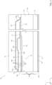
- Figure 2 shows, in lateral-sectional view in the same Cartesian (triaxial) reference system of axes X, Y, Z, of Figure 1 , an electronic device 50.
- the device 50 is a JBS diode, in analogy to what has been described with reference to Figure 1 ; however, the present invention is not limited to this device and also finds application to other types of electronic devices, in particular power devices, such as for example MOSFET, IGBT, MPS, Schottky diode, PN diode, PiN diode, etc.
- power devices such as for example MOSFET, IGBT, MPS, Schottky diode, PN diode, PiN diode, etc.
- the electronic device 50 comprises the elements described hereinbelow, illustrated with reference to Figure 2 .
- a semiconductor body 53 (e.g., including a substrate 53' and, optionally, one or more epitaxial layers 53" grown thereon), of N-type or P-type SiC (hereinafter non-limiting reference will be made to the sole N-type), is provided with a front surface 53a opposite to a rear surface 53b along the direction of the Z axis.
- the semiconductor body 53 includes, in the example illustrated in Figure 2 , the substrate 53' having the epitaxial layer 53" grown thereon acting as a drift layer of the electronic device 50, both of N-type SiC (in particular 4H-SiC, however other polytypes may be used such as, but not limited to, 2H-SiC, 3C-SiC and 6H-SiC).
- the substrate 53' has an N-type dopant concentration comprised between 1 ⁇ 10 19 at/cm 3 and 1 ⁇ 10 22 at/cm 3 and has a thickness, measured along the Z axis between the surfaces 53a and 53b, comprised between 300 ⁇ m and 450 pm, and in particular equal to about 360 ⁇ m.
- the drift layer 53" has a respective dopant concentration lower than the dopant concentration of the substrate and a thickness comprised, for example, between 5 and 15 ⁇ m.
- An ohmic contact layer 56 (for example of Nickel Silicide) extends on the rear surface 53b, and a metallization 57, in this example a cathode metallization, for example of Ti/NiV/Ag or Ti/NiV/Au, extends on the ohmic contact region 56.
- a metallization 57 in this example a cathode metallization, for example of Ti/NiV/Ag or Ti/NiV/Au, extends on the ohmic contact region 56.
- One or more P-type doped regions 59' extend in the semiconductor body 53 (in particular in the drift layer), facing the top surface 53a; each doped region 59' houses a respective ohmic contact (not shown and of known type) such that each doped region 59' forms a respective Junction-Barrier (JB) element 59.
- An edge termination region, or guard ring, 60 extends in the drift layer, faces the top surface 53a and completely surrounds (in plan view, on an XY plane defined by the axes X and Y) the JB elements 59.
- the edge termination region 60 may be omitted.
- An insulating layer 61 (of insulating or dielectric material, e.g. Silicon Oxide, TEOS) extends on the top surface 53a in such a way as to completely surround (in view on the XY plane) the JB elements 59 and to be partially superimposed on the guard ring 60 (when present).
- insulating or dielectric material e.g. Silicon Oxide, TEOS
- a metallization 58 in this example an anode metallization, for example of Ti/AlSiCu or Ni/AlSiCu, extends on a portion of the top surface 53a delimited externally by the insulating layer 61 (i.e., at the JB elements 59 / active area 54) and, partially, on the insulating layer 61.
- a passivation layer 69 of polymeric material such as polyimide (e.g., PIX) extends on the anode metallization 58 and on the insulating layer 61.
- the passivation layer 69 may alternatively be of a material from among: HfO 2 , ZrO 2 , TiO 2 , Ta 2 O 5 , TiN, ZnO, AZO, GZO.
- the passivation layer 69 is delimited by a top side 69a, a bottom side 69b, opposite to the top side 69a along the direction of the Z axis, and by lateral portions 69c which connect the top side 69a to the bottom side 69b.
- One or more Schottky diodes 62 are formed at the interface between the semiconductor body 53 and the anode metallization 58, laterally to the doped regions 59'.
- Schottky junctions semiconductor-metal are formed by portions of the semiconductor layer 53 in direct electrical contact with respective portions of the anode metallization 58.
- each ohmic contact extending in the respective doped region 59' provides an electrical connection having an electrical resistivity value lower than the electrical resistivity value of the doped region 59' housing it.
- the JB elements 59 are therefore P-i-N diodes.
- the region of the electronic device 50 which includes the JB elements 59 and the Schottky diodes 62 is an active area 54 of the electronic device 50.
- a lateral surface 53c of the semiconductor body 53 is present, for example extending substantially orthogonally to the top surface 53a.
- the lateral surface 53c is formed following a dicing, or singulation, step of a SiC wafer wherein a plurality of electronic devices 50 are provided.
- the dicing step has the function of separating an electronic device 50 from another device 50 of the same wafer.
- the dicing occurs at a scribe line (not shown) of the SiC wafer wherefrom the electronic device 50 is obtained; this scribe line surrounds at a distance, on the XY plane, the active region 54, the guard ring 60 and the insulating layer 61.
- a protection layer 74 of a resin such as for example Bakelite, extends above the passivation layer 69, to protect the electronic device 50 when inserted in a package (not shown).
- the passivation layer 69 is at least in part covered by an encapsulation structure 82 which extends below the passivation layer 69 and above the passivation layer 69.
- the encapsulation structure has the function of improving the adhesion of the passivation layer 69 to the rest of the electronic device 50 and therefore hereinafter it, and the layers forming it, will also be referred to as "adhesion improving structure", or “adhesion improving layers”, respectively.
- the encapsulation structure 82 comprises, in particular, a first portion 82a (first encapsulation layer or first adhesion improving layer) extending above the anode metallization 58 and the insulating layer 61 (in particular, in direct contact with the anode metallization 58 and the insulating layer 61), and below the passivation layer 69 (in particular, in direct contact with the passivation layer 69).
- first encapsulation layer 82a acts as an interface between the passivation layer 69 and the underlying layers, herein the metallization 58 and the insulating layer 61.
- the first encapsulation layer 82a extends throughout the entire extension of the bottom side 69b of the passivation layer 69; in particular, the first encapsulation layer 82a has a greater extension than the corresponding extension of the bottom side 69b of the passivation layer 69 (i.e., the first encapsulation layer 82a extends beyond the lateral portions 69c).
- the encapsulation structure 82 further comprises a second portion 82b (second encapsulation layer or second adhesion improving layer) extending on the top side 69a of the passivation layer 69 and on the lateral portions 69c, up to reaching and contacting the first encapsulation layer 82a wherein the first encapsulation layer protrudes beyond the lateral portions 69c.
- second portion 82b second encapsulation layer or second adhesion improving layer
- contact regions 70 between the first and the second encapsulation layers 82a, 82b provide a physical coupling element between the first and the second encapsulation layers 82a, 82b, configured to bond the second encapsulation layer 82b to the first encapsulation layer 82a, thus obviating a possible detachment of the passivation layer 69.
- the first and the second encapsulation layers 82a, 82b do not extend at the regions dedicated to housing the scribe line.
- the first encapsulation layer 82a extends throughout the entire extension of the bottom side 69b of the passivation layer 69 and, in particular, has an extension equal to the corresponding extension of the bottom side 69b of the passivation layer 69 (i.e., the first encapsulation layer 82a does not extend beyond the lateral portions 69c).
- the second encapsulation layer 82b extends, as well as on the passivation layer 69, also on the top surface 53a of the semiconductor body 53 on the right side of the representation of Figure 3 , and on the metallization 58 on the left side of the representation of Figure 3 , forming respective coupling regions 72.
- the coupling regions 72 comprise a respective contact portion 72a between the second encapsulation layer 82b and the underlying layers (top surface of the substrate 53c / metallization 58), and a respective lateral contact portion 72b between the second encapsulation layer 82b and the first encapsulation layer 82a.
- the passivation layer 69 is encapsulated, thus obviating a possible detachment of the passivation layer 69.
- the encapsulation structure 82 extends around the passivation layer 69 without interruptions (seamlessly) and without interfaces; in this case, both the first and the second encapsulation layers 82a, 82b are of a same material. In this embodiment, at the end of the manufacturing steps, the first and the second encapsulation layers 82a, 82b form a single body.
- first and the second encapsulation layers 82a, 82b are of respective materials different from each other.
- the materials of the first and the second encapsulation layers 82a, 82b are configured to have predetermined characteristics of adhesion to the material of the passivation layer 69 and to the underlying layers (here, the layers 58 and 61), in order to prevent delaminations and/or detachments of the passivation layer 69.
- the first and the second encapsulation layers 82a, 82b also act as protection for the passivation layer 69 to prevent cracks of the same.
- Materials for the aforementioned purposes include aluminum oxide (or alumina) Al 2 O 3 and hafnium oxide Hf 2 O 3 , in particular in case the passivation layer 69 is of a material from among polyimide, HfO 2 , ZrO 2 , TiO 2 , Ta 2 O 5 , TiN, ZnO, AZO, GZO.
- the Applicant has verified that a deposition by ALD (Atomic Layer Deposition) technique is effective in forming encapsulation layers 82a, 82b with characteristics of adhesion and protection suitable for the purposes of the present invention.
- the encapsulation layers 82a, 82b have, for example, a thickness comprised between 8 nm and 100 nm, in particular between 10 nm and 50 nm.
- the first and the second encapsulation layers 82a, 82b are both of Al 2 O 3 .
- first and the second encapsulation layers 82a, 82b are both of Hf 2 O 3 .
- the first encapsulation layer 82a is of Al 2 O 3 and the second encapsulation layer 82b is of Hf 2 O 3 .
- the first encapsulation layer 82a is of Hf 2 O 3 and the second encapsulation layer 82b is of Al 2 O 3 .
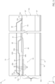
- Figure 4 illustrates an embodiment of the present invention. Elements common to Figures 2 and 3 are illustrated with the same reference numerals and are not further described. It should be noted that, although Figure 4 illustrates coupling regions 72 of the type illustrated in Figure 3 , the embodiment of Figure 4 is not limited to this aspect. In fact, coupling regions of the type illustrated in Figure 2 with the reference numeral 70 may equally apply to the embodiment of Figure 4 .
- each anchor element 84 is formed between the second encapsulation layer 82b and the passivation layer 69.
- each anchor element 84 extends through an opening or indentation 86 formed through the passivation layer 69.
- the opening 86 has a shape freely chosen during the design step, for example a circular, oval, generically polygonal, or irregular shape.
- Each anchor element 84 follows the shape of the opening 86 and is for further improving the bonding (adhesion) of the second encapsulation layer 82b to the passivation layer 69.
- the cavity 86 which houses the respective anchor element 84 therefore has a complementary shape with respect to the shape of the anchor element 84. In other words, each anchor element 84 completely fills the cavity housing it.
- Each anchor element 84 is of the same material as the second encapsulation layer 82b and therefore forms a single body, or monolithic structure, with the second encapsulation layer 82b.
- Each anchor element 84 is formed simultaneously with the second encapsulation layer 82b, for example during the step of forming (depositing) the material of the second encapsulation layer 82b.
- the openings 86 may be replaced by a general roughness or granularity of the top surface of the passivation layer 69.
- the Applicant has verified that characteristics of adhesion for the purpose of the present invention may be obtained, in one embodiment, by ALD deposition of the second encapsulation layer 82b; however, in the case of Figure 4 , other types of deposition may be used, for example CVD deposition, since the presence of the anchor elements 84 is per se sufficient to obtain the aforementioned characteristics of adhesion.
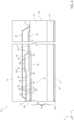
- Figure 5 illustrates a further embodiment, wherein a physical anchor 88 is formed between the passivation layer 69 and the semiconductor body 53.
- the anchor 88 of Figure 5 may apply to any of the previously described embodiments.
- the anchor element 88 protrudes from the passivation layer 69 (in particular, along the direction of the Z axis) and extends, through the first encapsulation layer 82a, inside the insulating layer 61, up to reaching the top surface 53a of the semiconductor body 53.
- the anchor element 88 anchors and bonds the passivation layer 69 to the insulating layer 61.
- the anchor element 88 is integral with the passivation layer 69 and, in particular, is an extension of the same passivation layer 69.
- the anchor element 88 therefore extends from the passivation layer 69 without interruptions (seamlessly) and without interfaces and is of the same material as the passivation layer 69.
- the anchor element 88 and the passivation layer 69 form a single, or monolithic, body.
- the anchor element 82 extends in, and fills, a through hole formed through the encapsulation layer 82a. This through hole has a shape freely chosen during the design step, for example a circular, oval or polygonal shape, with a diameter along the X axis equal to a few micrometers, for example between 2 and 5 ⁇ m.
- the anchor element 88 is formed outside the active area 54, and in particular outside the edge termination region 60; in other words, the anchor element 88 is interposed between the edge termination region 60 and the lateral surface 53c. In the event that the edge termination region 60 is not present, the anchor element 88 is formed outside the active area 54, i.e. between the active area 54 and the lateral surface 53c in an electrically passive region of the device.
- the anchor element 88 is patterned in such a way as to bond the passivation layer 69 to the insulating layer 61 and is for further improving the adhesion of the passivation layer 69, preventing and/or avoiding the delamination and/or the detachment of the passivation layer 69.
- the anchor element 88 is housed and fit into a housing or cavity extending in the insulating layer 61, in such a way as to couple and make the passivation layer 69 and the insulating layer 61 integral with each other.
- the cavity which houses the anchor element 88 has a complementary shape with respect to the shape of the anchor element 88. In other words, the anchor element 88 completely fills the cavity housing it.
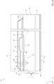
- Figure 6 illustrates a further embodiment, wherein one or more anchor elements 92 extend in respective one or more trenches 94 which traverse the passivation layer 69 throughout the entire thickness along the Z axis.
- the anchor elements 92 connect the first encapsulation layer 82a to the second encapsulation layer 82b.
- the trenches 94 are formed by steps of etching the passivation layer 69 and then the anchor elements 92 are formed by filling these trenches 94 during the step of forming the second encapsulation layer 82b and with the same material used to form the second encapsulation layer 82b. If allowed by the extension along the Z axis of the trenches 94, the anchor elements 92 and the second encapsulation layer 82b are formed simultaneously by ALD deposition; alternatively, a CVD deposition may be used to fill the trenches 94, forming the anchor elements 92, and to form simultaneously the second encapsulation layer 82b.
- the thickness of the passivation layer 69 might not be (typically, is not) uniform along the entire extension of the same, such trenches 94 and relative anchor elements 92 may be formed at the thinner portions (along the Z axis) of the passivation layer 69.
- Anchor elements of the type illustrated in Figure 6 may also be implemented in any of the embodiments previously described, in a per se evident manner.
- Figure 7 is based on Figure 6 (elements common with Figure 6 have the same reference numerals and are not further described).
- the connection regions 70 or 72 of Figures 2 or 3 are omitted.
- the second encapsulation layer does not extend on the lateral walls 69c of the passivation layer 69, or it extends only in part on the lateral walls 69c.
- the anchor elements 92 between the first and the second encapsulation layers 82a, 82b provide respective physical coupling elements between the first and the second encapsulation layers 82a, 82b, configured to bond the second encapsulation layer 82b to the first encapsulation layer 82a, encapsulating the passivation layer 69 and thus obviating a possible detachment of the passivation layer 69.
- Figure 7 shows a further embodiment of an electronic device 100.
- Figure 7 shows, in lateral sectional view in the same Cartesian (triaxial) reference system of axes X, Y, Z, of Figures 1-6 , the electronic device 100.
- the device 100 is a JBS diode, in analogy to what has been described with reference to Figures 1-6 ; however, the embodiment of Figure 7 is not limited to this JBS device and also finds application to other types of electronic devices, in particular power devices, such as for example MOSFET, IGBT, MPS, Schottky diode, PN diode, PiN diode, etc.
- the electronic device 100 comprises the elements described hereinafter, wherein elements common to the embodiments of Figures 2-6 are identified with the same reference numerals.
- a semiconductor body 53 (e.g., including a substrate 53' and, optionally, one or more epitaxial layers 53" grown thereon), of N-type or P-type SiC (hereinafter non-limiting reference will be made to the sole N-type), is provided with a front surface 53a opposite to a rear surface 53b along the direction of the Z axis.
- the semiconductor body 53 includes the substrate 53' having the epitaxial layer 53" grown thereon acting as a drift layer of the electronic device 100, both of N-type SiC (in particular 4H-SiC, however other polytypes may be used such as, but not limited to, 2H-SiC, 3C-SiC and 6H-SiC).
- the substrate 53' has an N-type dopant concentration comprised between 1 ⁇ 10 19 at/cm 3 and 1 ⁇ 10 22 at/cm 3 and has a thickness, measured along the Z axis between the surfaces 53a and 53b, comprised between 300 ⁇ m and 450 pm, and in particular equal to about 360 ⁇ m.
- the drift layer 53" has a respective dopant concentration lower than the dopant concentration of the substrate and a thickness comprised, for example, between 5 and 15 ⁇ m.
- An ohmic contact layer 56 (for example of Nickel Silicide) extends on the rear surface 53b, and a metallization 57, in this example a cathode metallization, for example of Ti/NiV/Ag or Ti/NiV/Au, extends on the ohmic contact region 56.
- a metallization 57 in this example a cathode metallization, for example of Ti/NiV/Ag or Ti/NiV/Au, extends on the ohmic contact region 56.
- One or more P-type doped regions 59' extend in the semiconductor body 53 (in particular in the drift layer), facing the top surface 53a; each doped region 59' houses a respective ohmic contact (not shown and of known type) such that each doped region 59' forms a respective Junction-Barrier (JB) element 59.
- An edge termination region, o guard ring, 60 in particular a further P-type doped region, extends in the drift layer, faces the top surface 53a and completely surrounds (in plan view, on an XY plane defined by the axes X and Y) the JB elements 59.
- the edge termination region 60 may be omitted.
- An insulating layer 61 (of insulating or dielectric material, e.g. Silicon Oxide, TEOS) extends on the top surface 53a in such a way as to completely surround (in view on the XY plane) the JB elements 59 and to be partially superimposed on the guard ring 60 (when present).
- insulating or dielectric material e.g. Silicon Oxide, TEOS
- a metallization 58 in this example an anode metallization, for example of Ti/AlSiCu or Ni/AlSiCu, extends on a portion of the top surface 53a delimited externally by the insulating layer 61 (i.e., at the JB elements 59 / active area 54) and, partially, on the insulating layer 61.
- the passivation layer 69 is delimited by a top side 69a, a bottom side 69b, opposite to the top side 69a along the Z axis direction, and by lateral portions 69c connecting the top side 69a to the bottom side 69b.
- One or more Schottky diodes 62 are formed at the interface between the semiconductor body 53 and the anode metallization 58, laterally to the doped regions 59'.
- Schottky junctions semiconductor-metal are formed by portions of the semiconductor layer 53 in direct electrical contact with respective portions of the anode metallization 58.
- each ohmic contact extending in the respective doped region 59' provides an electrical connection having an electrical resistivity value lower than the electrical resistivity value of the doped region 59' housing it.
- the JB elements 59 are therefore P-i-N diodes.
- the region of the electronic device 100 that includes the JB elements 59 and the Schottky diodes 62 is an active area 54 of the electronic device 100.
- a lateral surface 53c of the semiconductor body 53 is present, for example extending substantially orthogonally to the top surface 53a.
- the lateral surface 53c is formed following a dicing, or singulation, step of a SiC wafer wherein a plurality of electronic devices 100 are provided.
- the dicing step has the function of separating an electronic device 100 from another device 100 of the same wafer.
- the dicing occurs at a scribe line (not shown) of the SiC wafer wherefrom the electronic device 100 is obtained; this scribe line surrounds at a distance, on the XY plane, the active region 54, the guard ring 60 and the insulating layer 61.
- a protection layer 74 of a resin such as for example Bakelite, extends above the passivation layer 69, to protect the electronic device 50 when inserted in a package (not shown).
- an interface layer 102 extends continuously between the passivation layer 69 and the underlying metallization 58 and insulating layers 61.
- the interface layer 102 is in direct contact with the anode metallization 58 and the insulating layer 61 on one side, and with the passivation layer 69 on the opposite side.
- the interface layer 102 extends at least throughout the entire extension of the bottom side 69b of the passivation layer 69.
- the interface layer 102 does not extend at the regions dedicated to housing the scribe line.
- the interface layer 102 is of a material configured to have predetermined characteristics of adhesion to the material of the passivation layer 69 and to the layers 58 and 61, in order to prevent delaminations and/or detachments of the passivation layer 69.
- Materials for this purpose include aluminum oxide (or alumina) Al 2 O 3 and hafnium oxide Hf 2 O 3 .
- ALD Atomic Layer Deposition
- the interface layer 102 has, for example, a thickness comprised between 8 nm and 100 nm, in particular between 10 nm and 50 nm.
- the Applicant has verified that the interface layer 102 of Hf 2 O 3 or Al 2 O 3 possesses humidity barrier properties.
- An anchor element 88 as described with reference to Figure 5 , may be implemented in the embodiment of Figure 7 , in a per se evident manner and therefore not further described.
- Figure 8 shows a further embodiment of an electronic device 110, according to a further aspect of the present disclosure.
- Figure 8 shows, in lateral sectional view in the same Cartesian (triaxial) reference system of axes X, Y, Z, of Figures 1-7 , the electronic device 110.
- the device 110 is a JBS diode, in analogy to what has been described with reference to Figures 1-7 ; however, the embodiment of Figure 8 is not limited to this JBS device and also finds application to other types of electronic devices, in particular power devices, such as for example MOSFET, IGBT, MPS, Schottky diode, PN diode, PiN diode, etc.
- the electronic device 110 comprises the elements described hereinafter, wherein elements common to the embodiments of Figures 2-6 are identified with the same reference numerals.
- a semiconductor body 53 (e.g., including a substrate 53' and, optionally, one or more epitaxial layers 53" grown thereon), of N-type or P-type SiC (hereinafter non-limiting reference will be made to the sole N-type), is provided with a front surface 53a opposite to a rear surface 53b along the direction of the Z axis.
- the semiconductor body 53 includes the substrate 53' having the epitaxial layer 53" grown thereon acting as a drift layer of the electronic device 110, both of N-type SiC (in particular 4H-SiC, however other polytypes may be used such as, but not limited to, 2H-SiC, 3C-SiC and 6H-SiC).
- the substrate 53' has an N-type dopant concentration comprised between 1 ⁇ 10 19 at/cm 3 and 1 ⁇ 10 22 at/cm 3 and has a thickness, measured along the Z axis between the surfaces 53a and 53b, comprised between 300 ⁇ m and 450 pm, and in particular equal to about 360 ⁇ m.
- the drift layer 53" has a respective dopant concentration lower than the dopant concentration of the substrate and a thickness comprised, for example, between 5 and 15 ⁇ m.
- An ohmic contact layer 56 (for example of Nickel Silicide) extends on the rear surface 53b, and a metallization 57, in this example a cathode metallization, for example of Ti/NiV/Ag or Ti/NiV/Au, extends on the ohmic contact region 56.
- a metallization 57 in this example a cathode metallization, for example of Ti/NiV/Ag or Ti/NiV/Au, extends on the ohmic contact region 56.
- One or more P-type doped regions 59' extend in the semiconductor body 53 (in particular in the drift layer), facing the top surface 53a; each doped region 59' houses a respective ohmic contact (not shown and of known type) such that each doped region 59' forms a respective Junction-Barrier (JB) element 59.
- An edge termination region, o guard ring, 60 in particular a further P-type doped region, extends in the drift layer, faces the top surface 53a and completely surrounds (in plan view, on an XY plane defined by the axes X and Y) the JB elements 59.
- the edge termination region 60 may be omitted.
- An insulating layer 61 (of insulating or dielectric material, e.g. Silicon Oxide, TEOS) extends on the top surface 53a in such a way as to completely surround (in view on the XY plane) the JB elements 59 and to be partially superimposed on the guard ring 60 (when present).
- insulating or dielectric material e.g. Silicon Oxide, TEOS
- a metallization 58 in this example an anode metallization, for example of Ti/AlSiCu or Ni/AlSiCu, extends on a portion of the top surface 53a delimited externally by the insulating layer 61 (i.e., at the JB elements 59 / active area 54) and, partially, on the insulating layer 61.
- the passivation layer 69 is delimited by a top side 69a, a bottom side 69b, opposite to the top side 69a along the Z axis direction, and by lateral portions 69c connecting the top side 69a to the bottom side 69b.
- An interface layer 63 here of Silicon Nitride (SiN), extends above the anode metallization 58 and the insulating layer 61, and below the passivation layer 69.
- the interface layer 63 acts as an interface between the passivation layer 69 and the underlying layers, here the metallization 58 and the insulating layer 61 and allows the adhesion of the overlying passivation layer 69.
- One or more Schottky diodes 62 are formed at the interface between the semiconductor body 53 and the anode metallization 58, laterally to the doped regions 59'.
- Schottky junctions semiconductor-metal are formed by portions of the semiconductor layer 53 in direct electrical contact with respective portions of the anode metallization 58.
- each ohmic contact extending in the respective doped region 59' provides an electrical connection having an electrical resistivity value lower than the electrical resistivity value of the doped region 59' housing it.
- the JB elements 59 are therefore P-i-N diodes.
- the region of the electronic device 100 that includes the JB elements 59 and the Schottky diodes 62 is an active area 54 of the electronic device 110.
- a lateral surface 53c of the semiconductor body 53 is present, for example extending substantially orthogonally to the top surface 53a.
- the lateral surface 53c is formed following a dicing, or singulation, step of a SiC wafer wherein a plurality of electronic devices 110 are provided.
- the dicing step has the function of separating an electronic device 110 from another device 110 of the same wafer.
- the dicing occurs at a scribe line (not shown) of the SiC wafer wherefrom the electronic device 110 is obtained; this scribe line surrounds at a distance, on the XY plane, the active region 54, the guard ring 60 and the insulating layer 61.
- a protection layer 74 of a resin such as for example Bakelite, extends above the passivation layer 69, to protect the electronic device 50 when inserted in a package (not shown).
- the electronic device 110 further comprises a covering layer or cap layer 112 which extends on the top side 69a of the passivation layer 69 and on the lateral portions 69c, up to reaching and contacting the top surface 53a of the semiconductor body 53 on the right side of the representation of Figure 8 , and on the metallization 58 on the left side of the representation of Figure 8 , forming respective coupling regions 114.
- the coupling regions 114 provide respective physical coupling elements between the cap layer 112 and the underlying layers, laterally to the passivation layer 69, to bond or maintain the passivation layer 69 in position, thus obviating a possible detachment or delamination of the passivation layer 69.
- the cap layer 112 does not extend at the regions dedicated to housing the scribe line.
- Materials for the aforementioned purposes include aluminum oxide (or alumina) Al 2 O 3 and hafnium oxide Hf 2 O 3 , in particular in case the passivation layer 69 is of a material from among polyimide, HfO 2 , ZrO 2 , TiO 2 , Ta 2 O 5 , TiN, ZnO, AZO, GZO.
- the Applicant has verified that a deposition by ALD (Atomic Layer Deposition) technique is effective in forming the cap layer 112 with characteristics of adhesion and protection suitable for the purposes of the present invention.
- the cap layer 112 has, for example, a thickness comprised between 8 nm and 100 nm, in particular between 10 nm and 50 nm.
- the Applicant has verified that the cap layer 112 of Hf 2 O 3 or Al 2 O 3 possesses humidity barrier properties.
- the one or more adhesion improving layers described improve the adhesion of the passivation layer 69 to the rest of the device, preventing delamination phenomena. It is thus possible to form the passivation layer 69 in polymeric materials, ensuring high electrical performances of the electronic device 50, 100 (due to the high dielectric strength of the passivation layer 69) and eliminating, at the same time, structural problems linked to the possible detachment of the passivation layer 69 (e.g., following thermal or use cycles of the electronic device 50, 100).
- the manufacturing steps described allow manufacturing the electronic device 50 and, respectively, 100 comprising the respective adhesion improvement elements starting from a SiC wafer, without limitations resulting from the starting material (SiC).
Landscapes
- Electrodes Of Semiconductors (AREA)
- Internal Circuitry In Semiconductor Integrated Circuit Devices (AREA)
- Formation Of Insulating Films (AREA)
- Electroluminescent Light Sources (AREA)
- Bipolar Transistors (AREA)
Abstract
Description
- The present invention relates to an electronic device and to a method of manufacturing the electronic device, in particular wherein a passivation layer of the electronic device is provided with one or more adhesion improving layers.
- Silicon Carbide (SiC) is gaining considerable interest in the semiconductor industry, in particular for the manufacture of electronic components such as diodes or transistors, especially for power applications.
- Electronic devices formed in a silicon carbide substrate, in its different polytypes (for example, 3C-SiC, 4H-SiC, 6H-SiC), have numerous advantages such as low output resistance in conduction, low leakage current, resistance at high operating temperatures and high operating frequencies.
- However, the development and the manufacture of SiC-based electronic devices are limited by factors such as the electrical and mechanical properties of passivation layers (comprised in such electronic devices and, for example, extending on SiC semiconductor bodies of electronic devices). In particular, it is known to form the passivation layers using polymeric materials (e.g., polyimide) which allow to withstand high operating temperatures of the electronic devices and have high dielectric strength, for example higher than 400 kV/mm. In detail, the high dielectric strength of polymeric materials ensures that the passivation layers withstand high electric fields, and therefore high potential differences thereacross, without breaking or perforating ("electrical breakdown"), and therefore without becoming electrically conductive.
- However, polymeric materials have high coefficients of thermal expansion (CTE) (e.g., CTE=
43e -6 1/K for Polybenzobisoxazole material, or "PIX"), and it causes adhesion problems of the passivation layer to SiC, which has a lower coefficient of thermal expansion (CTE=3.8e-6 1/K). - In particular, such adhesion problems between the passivation layer and the SiC may arise during thermal cycling tests (performed for example between about -50°C and about +150°C) or during use of the electronic device, when the latter is subject to high thermal excursions (e.g., it is subject to operating temperature differences equal to, or greater than, about 200°C). Due to the high difference in CTE between the passivation layer and the SiC, such high thermal excursions generate mechanical stresses at an interface between the passivation layer and the SiC, which may lead to a(n) (at least partial) delamination of the passivation layer with respect to the SiC semiconductor body.
- If this delamination were sufficiently extended (e.g., it were such that no portion of the passivation layer is interposed between two metallizations of the electronic device set at different potentials, which are therefore separated from each other only by air), electric discharges may generate at said interface, leading to the damage of the same electronic device. In particular, the risk of damaging the electronic device increases when the latter is used in reverse bias conditions, due to the high voltage difference (e.g., greater than 1000 V) to withstand.
- Known solutions to this problem comprise the use of a plurality of dielectric layers of materials different from each other (e.g., Silicon Nitride, Silicon oxide and polyamide in succession to each other) to form a passivation multi-layer for limiting the mechanical stresses at the interface with the SiC semiconductor body.
-
Figure 1 shows, in lateral sectional view in a Cartesian (triaxial) reference system of axes X, Y, Z, a portion of an electronic device (here exemplarily a JBS, "Junction Barrier Schottky", diode) 1 of a known type. - The JBS
device 1 comprises asemiconductor body 3, of N-type SiC, provided with a surface 3a opposite to asurface 3b. The semiconductor body includes, for example, a substrate and one or more regions epitaxially grown on the substrate, of the N-type and having respective doping concentration values. The JBSdevice 1 also comprises multiple junction-barrier (JB)elements 9 in thesemiconductor body 3, facing the top surface 3a and each including a respective region implanted in thesemiconductor body 3, of the P-type, and an ohmic contact on the implanted region, at the level of the top surface 3a of thesemiconductor body 3. The JBSdevice 1 further comprises afirst metallization 8, which extends on the top surface 3a, in electrical contact with the junction-barrier elements 9 through the respective ohmic contacts. The JBSdevice 1 further comprises an edge termination region 10 (or guard ring), in particular a P-type implanted region, which completely surrounds theJB elements 9. - Schottky
diodes 12 are formed at the interface between theanode metallization 8 and thesemiconductor body 3, where semiconductor-metal Schottky junctions are formed. The region of theMPS device 1 which includes theJB elements 9 and the Schottky diodes 12 (i.e., the region contained within the guard ring 10) is anactive area 4 of theJBS device 1. - The JBS
device 1 further comprises asecond metallization 6, which extends on thebottom surface 3b. The first and thesecond metallizations JBS device 1. - An electrically
passive region 16 extends outside theedge termination region 10. - An
insulating layer 18, of insulating or dielectric material, in particular Silicon Oxide (SiO2), extends partially above theedge termination region 10. - The
first metallization 8 is in electrical contact with a portion of theedge termination region 10 where the latter is not covered by theinsulating layer 18, and also extends partially above theinsulating layer 18. Aninterface layer 20, here of Silicon Nitride (SiN), extends above thefirst metallization 8 and theinsulating layer 18. Furthermore, theJBS device 1 comprises apassivation layer 22, in particular of polyimide, which extends above theinterface layer 20. In other words, theinterface layer 20 acts as an interface between thepassivation layer 22 and the underlying layers, here thefirst metallization 8 and theinsulating layer 18. Theinterface layer 20 may be omitted; however, the Applicant has verified that theinterface layer 20 improves the adhesion of thepassivation layer 22 with the underlying layers. - A
protection layer 24, of a resin such as for example Bakelite, extends above thepassivation layer 22, to protect theJBS device 1 when inserted in a package (not shown). - However, although the
interface layer 20 improves, as said, the adhesion of thepassivation layer 22 with the underlying layers, some critical conditions of use or of thermal or thermo-mechanical test of theJBS device 1 may cause a delamination or partial detachment of thepassivation layer 22 from the interface layer 20 (due to the stress generated by the tests). This occurs in particular under conditions of stress caused by high use temperatures (e.g., above 150°C) and/or high thermal excursion (e.g., higher than 200°C). This effect, in addition to making theJBS 1 device structurally fragile, may be a contributing factor in the occurrence of undesired electric discharges which affect the electrical operation of theJBS 1 device. In fact, the Applicant has verified that in some conditions of thermo-mechanical or mechanical stress process following the assembling process, theinterface layer 20 has one or more local cracks throughout the entire thickness which, at thefirst metal layer 8, cause the generation of such electric discharges. These problems are all the more evident when theelectronic device 1 is subject to high thermal excursions and high voltage differences under reverse bias conditions. - The need to overcome the aforementioned problems is therefore felt.
- According to the present invention, an electronic device and a method of manufacturing the electronic device are provided, as defined in the attached claims.
- For a better understanding of the present invention, a preferred embodiment is now described, purely by way of non-limiting example, with reference to the attached drawings, wherein:
-
Figure 1 illustrates, in a cross-sectional view, an electronic device of known type; and -
Figures 2-8 illustrate, in cross-sectional view, respective electronic devices according to respective embodiments. -
Figure 2 shows, in lateral-sectional view in the same Cartesian (triaxial) reference system of axes X, Y, Z, ofFigure 1 , anelectronic device 50. In particular, thedevice 50 is a JBS diode, in analogy to what has been described with reference toFigure 1 ; however, the present invention is not limited to this device and also finds application to other types of electronic devices, in particular power devices, such as for example MOSFET, IGBT, MPS, Schottky diode, PN diode, PiN diode, etc. - The
electronic device 50 comprises the elements described hereinbelow, illustrated with reference toFigure 2 . - A semiconductor body 53 (e.g., including a substrate 53' and, optionally, one or more
epitaxial layers 53" grown thereon), of N-type or P-type SiC (hereinafter non-limiting reference will be made to the sole N-type), is provided with afront surface 53a opposite to arear surface 53b along the direction of the Z axis. Thesemiconductor body 53 includes, in the example illustrated inFigure 2 , the substrate 53' having theepitaxial layer 53" grown thereon acting as a drift layer of theelectronic device 50, both of N-type SiC (in particular 4H-SiC, however other polytypes may be used such as, but not limited to, 2H-SiC, 3C-SiC and 6H-SiC). For example, the substrate 53' has an N-type dopant concentration comprised between 1·1019 at/cm3 and 1·1022 at/cm3 and has a thickness, measured along the Z axis between thesurfaces drift layer 53" has a respective dopant concentration lower than the dopant concentration of the substrate and a thickness comprised, for example, between 5 and 15 µm. - An ohmic contact layer 56 (for example of Nickel Silicide) extends on the
rear surface 53b, and ametallization 57, in this example a cathode metallization, for example of Ti/NiV/Ag or Ti/NiV/Au, extends on theohmic contact region 56. - One or more P-type doped regions 59' extend in the semiconductor body 53 (in particular in the drift layer), facing the
top surface 53a; each doped region 59' houses a respective ohmic contact (not shown and of known type) such that each doped region 59' forms a respective Junction-Barrier (JB)element 59. An edge termination region, or guard ring, 60, in particular a further P-type doped region, extends in the drift layer, faces thetop surface 53a and completely surrounds (in plan view, on an XY plane defined by the axes X and Y) theJB elements 59. Theedge termination region 60 may be omitted. - An insulating layer 61 (of insulating or dielectric material, e.g. Silicon Oxide, TEOS) extends on the
top surface 53a in such a way as to completely surround (in view on the XY plane) theJB elements 59 and to be partially superimposed on the guard ring 60 (when present). - A
metallization 58, in this example an anode metallization, for example of Ti/AlSiCu or Ni/AlSiCu, extends on a portion of thetop surface 53a delimited externally by the insulating layer 61 (i.e., at theJB elements 59 / active area 54) and, partially, on theinsulating layer 61. - A
passivation layer 69 of polymeric material such as polyimide (e.g., PIX) extends on theanode metallization 58 and on theinsulating layer 61. - The
passivation layer 69 may alternatively be of a material from among: HfO2, ZrO2, TiO2, Ta2O5, TiN, ZnO, AZO, GZO. - The
passivation layer 69 is delimited by atop side 69a, abottom side 69b, opposite to thetop side 69a along the direction of the Z axis, and bylateral portions 69c which connect thetop side 69a to thebottom side 69b. - One or more Schottky
diodes 62 are formed at the interface between thesemiconductor body 53 and theanode metallization 58, laterally to the doped regions 59'. In particular, Schottky junctions (semiconductor-metal) are formed by portions of thesemiconductor layer 53 in direct electrical contact with respective portions of theanode metallization 58. - Furthermore, each ohmic contact extending in the respective doped region 59' provides an electrical connection having an electrical resistivity value lower than the electrical resistivity value of the doped region 59' housing it. The
JB elements 59 are therefore P-i-N diodes. - The region of the
electronic device 50 which includes theJB elements 59 and the Schottky diodes 62 (i.e., the region delimited by the guard ring 60) is anactive area 54 of theelectronic device 50. - Outside the
active area 54, i.e. beyond theedge termination region 60, alateral surface 53c of thesemiconductor body 53 is present, for example extending substantially orthogonally to thetop surface 53a. Thelateral surface 53c is formed following a dicing, or singulation, step of a SiC wafer wherein a plurality ofelectronic devices 50 are provided. The dicing step has the function of separating anelectronic device 50 from anotherdevice 50 of the same wafer. The dicing occurs at a scribe line (not shown) of the SiC wafer wherefrom theelectronic device 50 is obtained; this scribe line surrounds at a distance, on the XY plane, theactive region 54, theguard ring 60 and the insulatinglayer 61. - A
protection layer 74, of a resin such as for example Bakelite, extends above thepassivation layer 69, to protect theelectronic device 50 when inserted in a package (not shown). - According to one aspect of the present invention, the
passivation layer 69 is at least in part covered by anencapsulation structure 82 which extends below thepassivation layer 69 and above thepassivation layer 69. The encapsulation structure has the function of improving the adhesion of thepassivation layer 69 to the rest of theelectronic device 50 and therefore hereinafter it, and the layers forming it, will also be referred to as "adhesion improving structure", or "adhesion improving layers", respectively. - The
encapsulation structure 82 comprises, in particular, afirst portion 82a (first encapsulation layer or first adhesion improving layer) extending above theanode metallization 58 and the insulating layer 61 (in particular, in direct contact with theanode metallization 58 and the insulating layer 61), and below the passivation layer 69 (in particular, in direct contact with the passivation layer 69). In other words, thefirst encapsulation layer 82a acts as an interface between thepassivation layer 69 and the underlying layers, herein themetallization 58 and the insulatinglayer 61. - In one embodiment (
Figure 2 ) thefirst encapsulation layer 82a extends throughout the entire extension of thebottom side 69b of thepassivation layer 69; in particular, thefirst encapsulation layer 82a has a greater extension than the corresponding extension of thebottom side 69b of the passivation layer 69 (i.e., thefirst encapsulation layer 82a extends beyond thelateral portions 69c). - The
encapsulation structure 82 further comprises asecond portion 82b (second encapsulation layer or second adhesion improving layer) extending on thetop side 69a of thepassivation layer 69 and on thelateral portions 69c, up to reaching and contacting thefirst encapsulation layer 82a wherein the first encapsulation layer protrudes beyond thelateral portions 69c. In this manner,contact regions 70 between the first and thesecond encapsulation layers second encapsulation layers second encapsulation layer 82b to thefirst encapsulation layer 82a, thus obviating a possible detachment of thepassivation layer 69. - The first and the
second encapsulation layers - In a further embodiment, illustrated in
Figure 3 (elements common to those ofFigure 2 are identified with the same reference numerals and are not further described), thefirst encapsulation layer 82a extends throughout the entire extension of thebottom side 69b of thepassivation layer 69 and, in particular, has an extension equal to the corresponding extension of thebottom side 69b of the passivation layer 69 (i.e., thefirst encapsulation layer 82a does not extend beyond thelateral portions 69c). Thesecond encapsulation layer 82b extends, as well as on thepassivation layer 69, also on thetop surface 53a of thesemiconductor body 53 on the right side of the representation ofFigure 3 , and on themetallization 58 on the left side of the representation ofFigure 3 , formingrespective coupling regions 72. Thecoupling regions 72 comprise arespective contact portion 72a between thesecond encapsulation layer 82b and the underlying layers (top surface of thesubstrate 53c / metallization 58), and a respectivelateral contact portion 72b between thesecond encapsulation layer 82b and thefirst encapsulation layer 82a. In this manner, thepassivation layer 69 is encapsulated, thus obviating a possible detachment of thepassivation layer 69. - The aspects discussed hereinbelow apply to all embodiments of the present invention, in particular to those of
Figures 2 and3 described above and to those ofFigures 4-6 described below. - According to one aspect of the invention, the
encapsulation structure 82 extends around thepassivation layer 69 without interruptions (seamlessly) and without interfaces; in this case, both the first and thesecond encapsulation layers second encapsulation layers - In a further aspect of the invention, the first and the
second encapsulation layers - In general, the materials of the first and the
second encapsulation layers passivation layer 69 and to the underlying layers (here, thelayers 58 and 61), in order to prevent delaminations and/or detachments of thepassivation layer 69. The first and thesecond encapsulation layers passivation layer 69 to prevent cracks of the same. - Materials for the aforementioned purposes include aluminum oxide (or alumina) Al2O3 and hafnium oxide Hf2O3, in particular in case the
passivation layer 69 is of a material from among polyimide, HfO2, ZrO2, TiO2, Ta2O5, TiN, ZnO, AZO, GZO. - The Applicant has verified that a deposition by ALD (Atomic Layer Deposition) technique is effective in forming
encapsulation layers - In one aspect of the invention, the first and the
second encapsulation layers - In a further aspect of the invention, the first and the
second encapsulation layers - In a further aspect of the invention, the
first encapsulation layer 82a is of Al2O3 and thesecond encapsulation layer 82b is of Hf2O3. - In a further aspect of the invention, the
first encapsulation layer 82a is of Hf2O3 and thesecond encapsulation layer 82b is of Al2O3. - It is evident that other materials having characteristics of adhesion to the
passivation layer 69 may be chosen according to the material used for thepassivation layer 69. - In addition to the aforementioned characteristics of adhesion, the Applicant has verified that Hf2O3 and Al2O3 possess humidity barrier properties.
-
Figure 4 illustrates an embodiment of the present invention. Elements common toFigures 2 and3 are illustrated with the same reference numerals and are not further described. It should be noted that, althoughFigure 4 illustratescoupling regions 72 of the type illustrated inFigure 3 , the embodiment ofFigure 4 is not limited to this aspect. In fact, coupling regions of the type illustrated inFigure 2 with thereference numeral 70 may equally apply to the embodiment ofFigure 4 . - In the embodiment illustrated in
Figure 4 , one ormore anchor elements 84 are formed between thesecond encapsulation layer 82b and thepassivation layer 69. Referring toFigure 4 , eachanchor element 84 extends through an opening orindentation 86 formed through thepassivation layer 69. Theopening 86 has a shape freely chosen during the design step, for example a circular, oval, generically polygonal, or irregular shape. - Each
anchor element 84 follows the shape of theopening 86 and is for further improving the bonding (adhesion) of thesecond encapsulation layer 82b to thepassivation layer 69. Thecavity 86 which houses therespective anchor element 84 therefore has a complementary shape with respect to the shape of theanchor element 84. In other words, eachanchor element 84 completely fills the cavity housing it. - Each
anchor element 84 is of the same material as thesecond encapsulation layer 82b and therefore forms a single body, or monolithic structure, with thesecond encapsulation layer 82b. Eachanchor element 84 is formed simultaneously with thesecond encapsulation layer 82b, for example during the step of forming (depositing) the material of thesecond encapsulation layer 82b. - The
openings 86 may be replaced by a general roughness or granularity of the top surface of thepassivation layer 69. - As previously said, the Applicant has verified that characteristics of adhesion for the purpose of the present invention may be obtained, in one embodiment, by ALD deposition of the
second encapsulation layer 82b; however, in the case ofFigure 4 , other types of deposition may be used, for example CVD deposition, since the presence of theanchor elements 84 is per se sufficient to obtain the aforementioned characteristics of adhesion. -
Figure 5 (elements common toFigures 2-4 have the same reference numerals and are not further described) illustrates a further embodiment, wherein aphysical anchor 88 is formed between thepassivation layer 69 and thesemiconductor body 53. Theanchor 88 ofFigure 5 may apply to any of the previously described embodiments. Theanchor element 88 protrudes from the passivation layer 69 (in particular, along the direction of the Z axis) and extends, through thefirst encapsulation layer 82a, inside the insulatinglayer 61, up to reaching thetop surface 53a of thesemiconductor body 53. Theanchor element 88 anchors and bonds thepassivation layer 69 to the insulatinglayer 61. Theanchor element 88 is integral with thepassivation layer 69 and, in particular, is an extension of thesame passivation layer 69. Theanchor element 88 therefore extends from thepassivation layer 69 without interruptions (seamlessly) and without interfaces and is of the same material as thepassivation layer 69. In other words, theanchor element 88 and thepassivation layer 69 form a single, or monolithic, body. Theanchor element 82 extends in, and fills, a through hole formed through theencapsulation layer 82a. This through hole has a shape freely chosen during the design step, for example a circular, oval or polygonal shape, with a diameter along the X axis equal to a few micrometers, for example between 2 and 5 µm. Theanchor element 88 is formed outside theactive area 54, and in particular outside theedge termination region 60; in other words, theanchor element 88 is interposed between theedge termination region 60 and thelateral surface 53c. In the event that theedge termination region 60 is not present, theanchor element 88 is formed outside theactive area 54, i.e. between theactive area 54 and thelateral surface 53c in an electrically passive region of the device. Theanchor element 88 is patterned in such a way as to bond thepassivation layer 69 to the insulatinglayer 61 and is for further improving the adhesion of thepassivation layer 69, preventing and/or avoiding the delamination and/or the detachment of thepassivation layer 69. In particular, theanchor element 88 is housed and fit into a housing or cavity extending in the insulatinglayer 61, in such a way as to couple and make thepassivation layer 69 and the insulatinglayer 61 integral with each other. The cavity which houses theanchor element 88 has a complementary shape with respect to the shape of theanchor element 88. In other words, theanchor element 88 completely fills the cavity housing it. -
Figure 6 (elements common toFigures 2-5 have the same reference numerals and are not further described) illustrates a further embodiment, wherein one ormore anchor elements 92 extend in respective one ormore trenches 94 which traverse thepassivation layer 69 throughout the entire thickness along the Z axis. In this embodiment, theanchor elements 92 connect thefirst encapsulation layer 82a to thesecond encapsulation layer 82b. - In this embodiment, the
trenches 94 are formed by steps of etching thepassivation layer 69 and then theanchor elements 92 are formed by filling thesetrenches 94 during the step of forming thesecond encapsulation layer 82b and with the same material used to form thesecond encapsulation layer 82b. If allowed by the extension along the Z axis of thetrenches 94, theanchor elements 92 and thesecond encapsulation layer 82b are formed simultaneously by ALD deposition; alternatively, a CVD deposition may be used to fill thetrenches 94, forming theanchor elements 92, and to form simultaneously thesecond encapsulation layer 82b. - According to a non-limiting aspect of this embodiment, since the thickness of the
passivation layer 69 might not be (typically, is not) uniform along the entire extension of the same,such trenches 94 andrelative anchor elements 92 may be formed at the thinner portions (along the Z axis) of thepassivation layer 69. - Anchor elements of the type illustrated in
Figure 6 may also be implemented in any of the embodiments previously described, in a per se evident manner. - The embodiment of
Figure 7 is based onFigure 6 (elements common withFigure 6 have the same reference numerals and are not further described). In the embodiment ofFigure 7 , theconnection regions Figures 2 or3 are omitted. In other words, the second encapsulation layer does not extend on thelateral walls 69c of thepassivation layer 69, or it extends only in part on thelateral walls 69c. - The
anchor elements 92 between the first and thesecond encapsulation layers second encapsulation layers second encapsulation layer 82b to thefirst encapsulation layer 82a, encapsulating thepassivation layer 69 and thus obviating a possible detachment of thepassivation layer 69. -
Figure 7 shows a further embodiment of anelectronic device 100. -
Figure 7 shows, in lateral sectional view in the same Cartesian (triaxial) reference system of axes X, Y, Z, ofFigures 1-6 , theelectronic device 100. In particular, thedevice 100 is a JBS diode, in analogy to what has been described with reference toFigures 1-6 ; however, the embodiment ofFigure 7 is not limited to this JBS device and also finds application to other types of electronic devices, in particular power devices, such as for example MOSFET, IGBT, MPS, Schottky diode, PN diode, PiN diode, etc. - The
electronic device 100 comprises the elements described hereinafter, wherein elements common to the embodiments ofFigures 2-6 are identified with the same reference numerals. - A semiconductor body 53 (e.g., including a substrate 53' and, optionally, one or more
epitaxial layers 53" grown thereon), of N-type or P-type SiC (hereinafter non-limiting reference will be made to the sole N-type), is provided with afront surface 53a opposite to arear surface 53b along the direction of the Z axis. Thesemiconductor body 53 includes the substrate 53' having theepitaxial layer 53" grown thereon acting as a drift layer of theelectronic device 100, both of N-type SiC (in particular 4H-SiC, however other polytypes may be used such as, but not limited to, 2H-SiC, 3C-SiC and 6H-SiC). For example, the substrate 53' has an N-type dopant concentration comprised between 1·1019 at/cm3 and 1·1022 at/cm3 and has a thickness, measured along the Z axis between thesurfaces drift layer 53" has a respective dopant concentration lower than the dopant concentration of the substrate and a thickness comprised, for example, between 5 and 15 µm. - An ohmic contact layer 56 (for example of Nickel Silicide) extends on the
rear surface 53b, and ametallization 57, in this example a cathode metallization, for example of Ti/NiV/Ag or Ti/NiV/Au, extends on theohmic contact region 56. - One or more P-type doped regions 59' extend in the semiconductor body 53 (in particular in the drift layer), facing the
top surface 53a; each doped region 59' houses a respective ohmic contact (not shown and of known type) such that each doped region 59' forms a respective Junction-Barrier (JB)element 59. An edge termination region, o guard ring, 60, in particular a further P-type doped region, extends in the drift layer, faces thetop surface 53a and completely surrounds (in plan view, on an XY plane defined by the axes X and Y) theJB elements 59. Theedge termination region 60 may be omitted. - An insulating layer 61 (of insulating or dielectric material, e.g. Silicon Oxide, TEOS) extends on the
top surface 53a in such a way as to completely surround (in view on the XY plane) theJB elements 59 and to be partially superimposed on the guard ring 60 (when present). - A
metallization 58, in this example an anode metallization, for example of Ti/AlSiCu or Ni/AlSiCu, extends on a portion of thetop surface 53a delimited externally by the insulating layer 61 (i.e., at theJB elements 59 / active area 54) and, partially, on the insulatinglayer 61. - A
passivation layer 69 of polymeric material such as polyimide (e.g., PIX), extends on theanode metallization 58 and on the insulatinglayer 61. Thepassivation layer 69 is delimited by atop side 69a, abottom side 69b, opposite to thetop side 69a along the Z axis direction, and bylateral portions 69c connecting thetop side 69a to thebottom side 69b. - One or
more Schottky diodes 62 are formed at the interface between thesemiconductor body 53 and theanode metallization 58, laterally to the doped regions 59'. In particular, Schottky junctions (semiconductor-metal) are formed by portions of thesemiconductor layer 53 in direct electrical contact with respective portions of theanode metallization 58. - Furthermore, each ohmic contact extending in the respective doped region 59' provides an electrical connection having an electrical resistivity value lower than the electrical resistivity value of the doped region 59' housing it. The
JB elements 59 are therefore P-i-N diodes. - The region of the
electronic device 100 that includes theJB elements 59 and the Schottky diodes 62 (i.e., the region delimited by the guard ring 60) is anactive area 54 of theelectronic device 100. - Outside the
active area 54, i.e. beyond theedge termination region 60, alateral surface 53c of thesemiconductor body 53 is present, for example extending substantially orthogonally to thetop surface 53a. Thelateral surface 53c is formed following a dicing, or singulation, step of a SiC wafer wherein a plurality ofelectronic devices 100 are provided. The dicing step has the function of separating anelectronic device 100 from anotherdevice 100 of the same wafer. The dicing occurs at a scribe line (not shown) of the SiC wafer wherefrom theelectronic device 100 is obtained; this scribe line surrounds at a distance, on the XY plane, theactive region 54, theguard ring 60 and the insulatinglayer 61. - A
protection layer 74, of a resin such as for example Bakelite, extends above thepassivation layer 69, to protect theelectronic device 50 when inserted in a package (not shown). - According to one aspect of the present disclosure, an
interface layer 102 extends continuously between thepassivation layer 69 and theunderlying metallization 58 and insulatinglayers 61. In particular, theinterface layer 102 is in direct contact with theanode metallization 58 and the insulatinglayer 61 on one side, and with thepassivation layer 69 on the opposite side. - The
interface layer 102 extends at least throughout the entire extension of thebottom side 69b of thepassivation layer 69. Theinterface layer 102 does not extend at the regions dedicated to housing the scribe line. - The
interface layer 102 is of a material configured to have predetermined characteristics of adhesion to the material of thepassivation layer 69 and to thelayers passivation layer 69. Materials for this purpose include aluminum oxide (or alumina) Al2O3 and hafnium oxide Hf2O3. The Applicant has verified that a deposition by ALD (Atomic Layer Deposition) technique is effective in formingencapsulation layers interface layer 102 has, for example, a thickness comprised between 8 nm and 100 nm, in particular between 10 nm and 50 nm. In addition to the aforementioned characteristics of adhesion, the Applicant has verified that theinterface layer 102 of Hf2O3 or Al2O3 possesses humidity barrier properties. - An
anchor element 88, as described with reference toFigure 5 , may be implemented in the embodiment ofFigure 7 , in a per se evident manner and therefore not further described. -
Figure 8 shows a further embodiment of anelectronic device 110, according to a further aspect of the present disclosure. -
Figure 8 shows, in lateral sectional view in the same Cartesian (triaxial) reference system of axes X, Y, Z, ofFigures 1-7 , theelectronic device 110. In particular, thedevice 110 is a JBS diode, in analogy to what has been described with reference toFigures 1-7 ; however, the embodiment ofFigure 8 is not limited to this JBS device and also finds application to other types of electronic devices, in particular power devices, such as for example MOSFET, IGBT, MPS, Schottky diode, PN diode, PiN diode, etc. - The
electronic device 110 comprises the elements described hereinafter, wherein elements common to the embodiments ofFigures 2-6 are identified with the same reference numerals. - A semiconductor body 53 (e.g., including a substrate 53' and, optionally, one or more
epitaxial layers 53" grown thereon), of N-type or P-type SiC (hereinafter non-limiting reference will be made to the sole N-type), is provided with afront surface 53a opposite to arear surface 53b along the direction of the Z axis. Thesemiconductor body 53 includes the substrate 53' having theepitaxial layer 53" grown thereon acting as a drift layer of theelectronic device 110, both of N-type SiC (in particular 4H-SiC, however other polytypes may be used such as, but not limited to, 2H-SiC, 3C-SiC and 6H-SiC). For example, the substrate 53' has an N-type dopant concentration comprised between 1·1019 at/cm3 and 1·1022 at/cm3 and has a thickness, measured along the Z axis between thesurfaces drift layer 53" has a respective dopant concentration lower than the dopant concentration of the substrate and a thickness comprised, for example, between 5 and 15 µm. - An ohmic contact layer 56 (for example of Nickel Silicide) extends on the
rear surface 53b, and ametallization 57, in this example a cathode metallization, for example of Ti/NiV/Ag or Ti/NiV/Au, extends on theohmic contact region 56. - One or more P-type doped regions 59' extend in the semiconductor body 53 (in particular in the drift layer), facing the
top surface 53a; each doped region 59' houses a respective ohmic contact (not shown and of known type) such that each doped region 59' forms a respective Junction-Barrier (JB)element 59. An edge termination region, o guard ring, 60, in particular a further P-type doped region, extends in the drift layer, faces thetop surface 53a and completely surrounds (in plan view, on an XY plane defined by the axes X and Y) theJB elements 59. Theedge termination region 60 may be omitted. - An insulating layer 61 (of insulating or dielectric material, e.g. Silicon Oxide, TEOS) extends on the
top surface 53a in such a way as to completely surround (in view on the XY plane) theJB elements 59 and to be partially superimposed on the guard ring 60 (when present). - A
metallization 58, in this example an anode metallization, for example of Ti/AlSiCu or Ni/AlSiCu, extends on a portion of thetop surface 53a delimited externally by the insulating layer 61 (i.e., at theJB elements 59 / active area 54) and, partially, on the insulatinglayer 61. - A
passivation layer 69 of polymeric material such as polyimide (e.g., PIX), extends on theanode metallization 58 and on the insulatinglayer 61. Thepassivation layer 69 is delimited by atop side 69a, abottom side 69b, opposite to thetop side 69a along the Z axis direction, and bylateral portions 69c connecting thetop side 69a to thebottom side 69b. - An
interface layer 63, here of Silicon Nitride (SiN), extends above theanode metallization 58 and the insulatinglayer 61, and below thepassivation layer 69. In other words, theinterface layer 63 acts as an interface between thepassivation layer 69 and the underlying layers, here themetallization 58 and the insulatinglayer 61 and allows the adhesion of theoverlying passivation layer 69. - One or
more Schottky diodes 62 are formed at the interface between thesemiconductor body 53 and theanode metallization 58, laterally to the doped regions 59'. In particular, Schottky junctions (semiconductor-metal) are formed by portions of thesemiconductor layer 53 in direct electrical contact with respective portions of theanode metallization 58. - Furthermore, each ohmic contact extending in the respective doped region 59' provides an electrical connection having an electrical resistivity value lower than the electrical resistivity value of the doped region 59' housing it. The
JB elements 59 are therefore P-i-N diodes. - The region of the
electronic device 100 that includes theJB elements 59 and the Schottky diodes 62 (i.e., the region delimited by the guard ring 60) is anactive area 54 of theelectronic device 110. - Outside the
active area 54, i.e. beyond theedge termination region 60, alateral surface 53c of thesemiconductor body 53 is present, for example extending substantially orthogonally to thetop surface 53a. Thelateral surface 53c is formed following a dicing, or singulation, step of a SiC wafer wherein a plurality ofelectronic devices 110 are provided. The dicing step has the function of separating anelectronic device 110 from anotherdevice 110 of the same wafer. The dicing occurs at a scribe line (not shown) of the SiC wafer wherefrom theelectronic device 110 is obtained; this scribe line surrounds at a distance, on the XY plane, theactive region 54, theguard ring 60 and the insulatinglayer 61. - A
protection layer 74, of a resin such as for example Bakelite, extends above thepassivation layer 69, to protect theelectronic device 50 when inserted in a package (not shown). - The
electronic device 110 further comprises a covering layer orcap layer 112 which extends on thetop side 69a of thepassivation layer 69 and on thelateral portions 69c, up to reaching and contacting thetop surface 53a of thesemiconductor body 53 on the right side of the representation ofFigure 8 , and on themetallization 58 on the left side of the representation ofFigure 8 , formingrespective coupling regions 114. In this manner, thecoupling regions 114 provide respective physical coupling elements between thecap layer 112 and the underlying layers, laterally to thepassivation layer 69, to bond or maintain thepassivation layer 69 in position, thus obviating a possible detachment or delamination of thepassivation layer 69. - The
cap layer 112 does not extend at the regions dedicated to housing the scribe line. - The material of the
cap layer 112 is configured to have predetermined characteristics of adhesion to the material to thepassivation layer 69 and underlying layers at coupling regions 114 (here, layers 58 and 53"). - Materials for the aforementioned purposes include aluminum oxide (or alumina) Al2O3 and hafnium oxide Hf2O3, in particular in case the
passivation layer 69 is of a material from among polyimide, HfO2, ZrO2, TiO2, Ta2O5, TiN, ZnO, AZO, GZO. - The Applicant has verified that a deposition by ALD (Atomic Layer Deposition) technique is effective in forming the
cap layer 112 with characteristics of adhesion and protection suitable for the purposes of the present invention. Thecap layer 112 has, for example, a thickness comprised between 8 nm and 100 nm, in particular between 10 nm and 50 nm. - In addition to the aforementioned characteristics of adhesion, the Applicant has verified that the
cap layer 112 of Hf2O3 or Al2O3 possesses humidity barrier properties. - In a per se evident manner and therefore not further described, it is possible to implement, in the embodiment of
Figure 8 , theindentations 86 with therespective elements 84 described with reference toFigure 4 and/or theanchor element 88 described with reference toFigure 5 . - From an examination of the characteristics of the invention made according to the present invention the advantages that it affords are evident.
- In particular, the one or more adhesion improving layers described improve the adhesion of the
passivation layer 69 to the rest of the device, preventing delamination phenomena. It is thus possible to form thepassivation layer 69 in polymeric materials, ensuring high electrical performances of theelectronic device 50, 100 (due to the high dielectric strength of the passivation layer 69) and eliminating, at the same time, structural problems linked to the possible detachment of the passivation layer 69 (e.g., following thermal or use cycles of theelectronic device 50, 100). - Consequently, the risk of damaging the
electronic device electronic device - The manufacturing steps described allow manufacturing the
electronic device 50 and, respectively, 100 comprising the respective adhesion improvement elements starting from a SiC wafer, without limitations resulting from the starting material (SiC). - Finally, it is clear that modifications and variations may be made to the invention described and illustrated herein without thereby departing from the scope of the present invention, as defined in the attached claims.
- In particular, although the present invention has been described with explicit reference to SiC as the starting substrate material, the present invention also applies to devices based on substrates of other semiconductor materials, such as for example Silicon, GaN, etc.
Claims (16)
- An electronic device (50), comprising:a solid body (53, 58, 61) including an electrical terminal (58) of the electronic device on the solid body (53) ;a passivation layer (69) on the electrical terminal (58), of a first material, having a top surface (69a), a bottom surface (69b) facing the solid body and lateral surfaces (69c) which connect the top surface (69a) to the bottom surface (69b),an encapsulation layer (82b) of a second material having predefined characteristics of adhesion to the first material, extending continuously on the top surface (69a) of the passivation layer (69), on the lateral surfaces (69c) of the passivation layer (69), and on the solid body (53, 58, 61) laterally to said lateral surfaces (69c) of the passivation layer (69),characterized in that the top surface (69a) of the passivation layer (69) has one or more indentations (86) or roughness.
- The electronic device according to claim 1, wherein the encapsulation layer (82b) extends in part within said one or more indentations (86) or roughness of the passivation layer (69), thus forming respective one or more anchor elements (84).
- The electronic device according to claim 2, wherein the one or more anchor elements (84) are of the second material and form a single body, or monolithic structure, with the encapsulation layer (82b).
- The electronic device according to anyone of the preceding claims, wherein the encapsulation layer (82b) extends in direct physical contact with the top surface (69a) of the passivation layer (69).
- The electronic device according to claim 1, wherein the second material is one of Al2O3 and Hf2O3.
- The electronic device according to anyone of the preceding claims, further comprising an interface layer (82a) between the solid body (53) and the passivation layer (69), in direct contact with the passivation layer (69).
- The electronic device according to claim 6, wherein the encapsulation layer (82b) and the interface layer (82a) are of a same material or of different materials, from among: Al2O3 and Hf2O3.
- The electronic device according to anyone of the preceding claims, wherein the solid body comprises a semiconductor body (53) of Silicon Carbide.
- The electronic device according to claim 8, wherein the solid body further comprises an insulating layer (61) on a surface (53a) of the semiconductor body (53), the electrical terminal (58) extending in part on the surface (53a) of the semiconductor body (53) and in part on the insulating layer (61),said passivation layer completely covering the electrical terminal (58) and the insulating layer (61),said first adhesion improving layer (82a) extending in direct contact with the electrical terminal (58) and the insulating layer (61) forming a first interface between the electrical terminal (58) and a second interface between the passivation layer (69) and the insulating layer (61).
- The electronic device according to anyone of the preceding claims, wherein the first material is one among: polymeric material, polyimide or PIX, HfO2, ZrO2, TiO2, Ta2O5, TiN, ZnO, AZO, GZO.
- The electronic device according to any of the preceding claims, chosen from the group comprising: a Schottky diode, a PiN diode, a PN diode, an MPS device, a JBS diode, a MOSFET, an IGBT, a power device.
- A method for manufacturing an electronic device (50), comprising the steps of:providing a solid body (53, 58, 61) including an electrical terminal (58) of the electronic device on the solid body (53);forming, on the electrical terminal (58), a passivation layer (69) of a first material and having a top surface (69a), a bottom surface (69b) facing the solid body and lateral surfaces (69c) which connect the top surface (69a) to the bottom surface (69b);forming an encapsulation layer (82b) extending continuously on the top surface (69a) of the passivation layer (69), on the lateral surfaces (69c) of the passivation layer (69) and on the solid body (53, 58, 61) laterally to said lateral surfaces (69c) of the passivation layer (69), wherein the encapsulation layer (82b) is of a second material having predefined characteristics of adhesion to the first material,characterized by further comprising the step of forming, on the top surface (69a) of the passivation layer (69), one or more indentations (86) or roughness.
- The method according to claim 12, wherein forming the encapsulation layer (82b) comprises forming part of the encapsulation layer (82b) within said one or more indentations (86) or roughness of the passivation layer (69), thus forming respective one or more anchor elements (84).
- The method according to claim 13, wherein the one or more anchor elements (84) are of the second material and form a single body, or monolithic structure, with the encapsulation layer (82b).
- The method according to anyone of claims 12-14, wherein the encapsulation layer (82b) extends in direct physical contact with the top surface (69a) of the passivation layer (69).
- The method according to anyone of claims 12-15, further comprising the step of forming an interface layer (82a) between the solid body (53) and the passivation layer (69), in direct contact with the passivation layer (69).
Applications Claiming Priority (2)
| Application Number | Priority Date | Filing Date | Title |
|---|---|---|---|
| IT102022000024396A IT202200024396A1 (en) | 2022-11-25 | 2022-11-25 | SIC-BASED ELECTRONIC DEVICE WITH MULTILAYER AND MULTIFUNCTIONAL PASSIVATION, AND ELECTRONIC DEVICE MANUFACTURING METHOD |
| EP23207872.5A EP4386829A3 (en) | 2022-11-25 | 2023-11-06 | Sic-based electronic device with multilayer and multifunctional passivation, and method of manufacturing the electronic device |
Related Parent Applications (1)
| Application Number | Title | Priority Date | Filing Date |
|---|---|---|---|
| EP23207872.5A Division EP4386829A3 (en) | 2022-11-25 | 2023-11-06 | Sic-based electronic device with multilayer and multifunctional passivation, and method of manufacturing the electronic device |
Publications (2)
| Publication Number | Publication Date |
|---|---|
| EP4521456A2 true EP4521456A2 (en) | 2025-03-12 |
| EP4521456A3 EP4521456A3 (en) | 2025-05-14 |
Family
ID=85122362
Family Applications (3)
| Application Number | Title | Priority Date | Filing Date |
|---|---|---|---|
| EP24223383.1A Pending EP4521456A3 (en) | 2022-11-25 | 2023-11-06 | Sic-based electronic device with multilayer and multifunctional passivation, and method of manufacturing the electronic device |
| EP23207872.5A Pending EP4386829A3 (en) | 2022-11-25 | 2023-11-06 | Sic-based electronic device with multilayer and multifunctional passivation, and method of manufacturing the electronic device |
| EP24198132.3A Pending EP4451323A3 (en) | 2022-11-25 | 2023-11-06 | Sic-based electronic device with multilayer and multifunctional passivation, and method of manufacturing the electronic device |
Family Applications After (2)
| Application Number | Title | Priority Date | Filing Date |
|---|---|---|---|
| EP23207872.5A Pending EP4386829A3 (en) | 2022-11-25 | 2023-11-06 | Sic-based electronic device with multilayer and multifunctional passivation, and method of manufacturing the electronic device |
| EP24198132.3A Pending EP4451323A3 (en) | 2022-11-25 | 2023-11-06 | Sic-based electronic device with multilayer and multifunctional passivation, and method of manufacturing the electronic device |
Country Status (3)
| Country | Link |
|---|---|
| US (1) | US20240178092A1 (en) |
| EP (3) | EP4521456A3 (en) |
| IT (1) | IT202200024396A1 (en) |
Families Citing this family (1)
| Publication number | Priority date | Publication date | Assignee | Title |
|---|---|---|---|---|
| US20250391785A1 (en) | 2024-06-19 | 2025-12-25 | Stmicroelectronics International N.V. | Sic-based electronic device with enhanced robustness and method for manufacturing the electronic device |
Family Cites Families (4)
| Publication number | Priority date | Publication date | Assignee | Title |
|---|---|---|---|---|
| WO2015033623A1 (en) * | 2013-09-05 | 2015-03-12 | 三菱電機株式会社 | Semiconductor device and method for manufacturing same |
| CN110838471B (en) * | 2018-08-16 | 2025-01-14 | 飞锃半导体(上海)有限公司 | Chip edge structure and manufacturing method |
| JP7758501B2 (en) * | 2020-09-04 | 2025-10-22 | エスティーマイクロエレクトロニクス エス.アール.エル. | Method for manufacturing elements of electronic devices with improved reliability, and related elements, electronic devices, and electronic equipment |
| EP3975265A1 (en) * | 2020-09-28 | 2022-03-30 | Nexperia B.V. | A semiconductor device and a method of manufacturing of a semiconductor device |
-
2022
- 2022-11-25 IT IT102022000024396A patent/IT202200024396A1/en unknown
-
2023
- 2023-11-06 EP EP24223383.1A patent/EP4521456A3/en active Pending
- 2023-11-06 EP EP23207872.5A patent/EP4386829A3/en active Pending
- 2023-11-06 EP EP24198132.3A patent/EP4451323A3/en active Pending
- 2023-11-09 US US18/505,569 patent/US20240178092A1/en active Pending
Also Published As
| Publication number | Publication date |
|---|---|
| EP4521456A3 (en) | 2025-05-14 |
| EP4451323A3 (en) | 2025-01-08 |
| US20240178092A1 (en) | 2024-05-30 |
| EP4386829A2 (en) | 2024-06-19 |
| EP4386829A3 (en) | 2024-08-21 |
| IT202200024396A1 (en) | 2024-05-25 |
| EP4451323A2 (en) | 2024-10-23 |
Similar Documents
| Publication | Publication Date | Title |
|---|---|---|
| EP4191663B1 (en) | Method of manufacturing a sic-based electronic device with a passivation layer and an anchoring element and electronic device manufactured thereby | |
| CN102428581B (en) | Optoelectronic devices | |
| US9000476B2 (en) | Optoelectronic component | |
| US10971620B2 (en) | Method for producing a semiconductor arrangement | |
| EP4084064B1 (en) | Semiconductor device | |
| EP4187621A1 (en) | Sic-based electronic device with enhanced robustness, and method for manufacturing the electronic device | |
| EP4451323A2 (en) | Sic-based electronic device with multilayer and multifunctional passivation, and method of manufacturing the electronic device | |
| CN113678261A (en) | Semiconductor device and semiconductor module | |
| CN105765723A (en) | Optoelectronic semiconductor chip with built-in ESD protection | |
| US12283534B2 (en) | Power semiconductor devices with improved overcoat adhesion and/or protection | |
| EP3965149B1 (en) | Manufacturing method of an element of an electronic device having improved reliability, and related element, electronic device and electronic apparatus | |
| CN219591404U (en) | Electronic device | |
| CN223390546U (en) | An electronic device | |
| CN221994453U (en) | An electronic device | |
| CN219180514U (en) | Semiconductor Devices and Electronic Devices | |
| EP4668328A1 (en) | Sic-based electronic device with enhanced robustness and method for manufacturing the electronic device | |
| EP4669051A1 (en) | Electronic device based on sic having improved electrical performances and manufacturing method | |
| JP2026012639A (en) | SiC-based electronic devices with improved electrical performance and manufacturing methods | |
| JP2026004248A (en) | SIC-BASED ELECTRONIC DEVICES WITH ENHANCED ROBUSTNESS AND METHODS FOR MANUFACTURING THEM - Patent application | |
| CN116190457A (en) | SIC-based electronic device with enhanced robustness and method of fabricating the electronic device | |
| EP4687409A1 (en) | Electronic device with improved reliability | |
| KR100612187B1 (en) | Manufacturing method of schottky barrier diode | |
| CN121463498A (en) | Electronic device with improved reliability | |
| JP2009283750A (en) | Semiconductor device, and method for manufacturing thereof |
Legal Events
| Date | Code | Title | Description |
|---|---|---|---|
| PUAI | Public reference made under article 153(3) epc to a published international application that has entered the european phase |
Free format text: ORIGINAL CODE: 0009012 |
|
| STAA | Information on the status of an ep patent application or granted ep patent |
Free format text: STATUS: THE APPLICATION HAS BEEN PUBLISHED |
|
| AC | Divisional application: reference to earlier application |
Ref document number: 4386829 Country of ref document: EP Kind code of ref document: P |
|
| AK | Designated contracting states |
Kind code of ref document: A2 Designated state(s): AL AT BE BG CH CY CZ DE DK EE ES FI FR GB GR HR HU IE IS IT LI LT LU LV MC ME MK MT NL NO PL PT RO RS SE SI SK SM TR |
|
| PUAL | Search report despatched |
Free format text: ORIGINAL CODE: 0009013 |
|
| AK | Designated contracting states |
Kind code of ref document: A3 Designated state(s): AL AT BE BG CH CY CZ DE DK EE ES FI FR GB GR HR HU IE IS IT LI LT LU LV MC ME MK MT NL NO PL PT RO RS SE SI SK SM TR |
|
| RIC1 | Information provided on ipc code assigned before grant |
Ipc: H10D 62/832 20250101ALN20250407BHEP Ipc: H10D 62/10 20250101ALN20250407BHEP Ipc: H10D 8/01 20250101ALN20250407BHEP Ipc: H01L 23/00 20060101ALI20250407BHEP Ipc: H01L 23/29 20060101ALI20250407BHEP Ipc: H01L 23/31 20060101AFI20250407BHEP |
|
| STAA | Information on the status of an ep patent application or granted ep patent |
Free format text: STATUS: REQUEST FOR EXAMINATION WAS MADE |
|
| 17P | Request for examination filed |
Effective date: 20251023 |