EP4521449A1 - Procédé de fabrication d'une puce électronique comprenant des piliers de connexion pour un assemblage par frittage - Google Patents
Procédé de fabrication d'une puce électronique comprenant des piliers de connexion pour un assemblage par frittage Download PDFInfo
- Publication number
- EP4521449A1 EP4521449A1 EP24198761.9A EP24198761A EP4521449A1 EP 4521449 A1 EP4521449 A1 EP 4521449A1 EP 24198761 A EP24198761 A EP 24198761A EP 4521449 A1 EP4521449 A1 EP 4521449A1
- Authority
- EP
- European Patent Office
- Prior art keywords
- pillar
- end portion
- chip
- manufacturing
- electronic chip
- Prior art date
- Legal status (The legal status is an assumption and is not a legal conclusion. Google has not performed a legal analysis and makes no representation as to the accuracy of the status listed.)
- Granted
Links
Images


Classifications
-
- H—ELECTRICITY
- H10—SEMICONDUCTOR DEVICES; ELECTRIC SOLID-STATE DEVICES NOT OTHERWISE PROVIDED FOR
- H10W—GENERIC PACKAGES, INTERCONNECTIONS, CONNECTORS OR OTHER CONSTRUCTIONAL DETAILS OF DEVICES COVERED BY CLASS H10
- H10W72/00—Interconnections or connectors in packages
- H10W72/20—Bump connectors, e.g. solder bumps or copper pillars; Dummy bumps; Thermal bumps
-
- H—ELECTRICITY
- H10—SEMICONDUCTOR DEVICES; ELECTRIC SOLID-STATE DEVICES NOT OTHERWISE PROVIDED FOR
- H10W—GENERIC PACKAGES, INTERCONNECTIONS, CONNECTORS OR OTHER CONSTRUCTIONAL DETAILS OF DEVICES COVERED BY CLASS H10
- H10W72/00—Interconnections or connectors in packages
- H10W72/01—Manufacture or treatment
- H10W72/012—Manufacture or treatment of bump connectors, dummy bumps or thermal bumps
-
- H—ELECTRICITY
- H10—SEMICONDUCTOR DEVICES; ELECTRIC SOLID-STATE DEVICES NOT OTHERWISE PROVIDED FOR
- H10W—GENERIC PACKAGES, INTERCONNECTIONS, CONNECTORS OR OTHER CONSTRUCTIONAL DETAILS OF DEVICES COVERED BY CLASS H10
- H10W72/00—Interconnections or connectors in packages
- H10W72/071—Connecting or disconnecting
- H10W72/072—Connecting or disconnecting of bump connectors
-
- H—ELECTRICITY
- H10—SEMICONDUCTOR DEVICES; ELECTRIC SOLID-STATE DEVICES NOT OTHERWISE PROVIDED FOR
- H10W—GENERIC PACKAGES, INTERCONNECTIONS, CONNECTORS OR OTHER CONSTRUCTIONAL DETAILS OF DEVICES COVERED BY CLASS H10
- H10W72/00—Interconnections or connectors in packages
- H10W72/01—Manufacture or treatment
- H10W72/012—Manufacture or treatment of bump connectors, dummy bumps or thermal bumps
- H10W72/01215—Manufacture or treatment of bump connectors, dummy bumps or thermal bumps forming coatings
-
- H—ELECTRICITY
- H10—SEMICONDUCTOR DEVICES; ELECTRIC SOLID-STATE DEVICES NOT OTHERWISE PROVIDED FOR
- H10W—GENERIC PACKAGES, INTERCONNECTIONS, CONNECTORS OR OTHER CONSTRUCTIONAL DETAILS OF DEVICES COVERED BY CLASS H10
- H10W72/00—Interconnections or connectors in packages
- H10W72/01—Manufacture or treatment
- H10W72/012—Manufacture or treatment of bump connectors, dummy bumps or thermal bumps
- H10W72/01231—Manufacture or treatment of bump connectors, dummy bumps or thermal bumps using blanket deposition
- H10W72/01233—Manufacture or treatment of bump connectors, dummy bumps or thermal bumps using blanket deposition in liquid form, e.g. spin coating, spray coating or immersion coating
- H10W72/01235—Manufacture or treatment of bump connectors, dummy bumps or thermal bumps using blanket deposition in liquid form, e.g. spin coating, spray coating or immersion coating by plating, e.g. electroless plating or electroplating
-
- H—ELECTRICITY
- H10—SEMICONDUCTOR DEVICES; ELECTRIC SOLID-STATE DEVICES NOT OTHERWISE PROVIDED FOR
- H10W—GENERIC PACKAGES, INTERCONNECTIONS, CONNECTORS OR OTHER CONSTRUCTIONAL DETAILS OF DEVICES COVERED BY CLASS H10
- H10W72/00—Interconnections or connectors in packages
- H10W72/01—Manufacture or treatment
- H10W72/012—Manufacture or treatment of bump connectors, dummy bumps or thermal bumps
- H10W72/01251—Changing the shapes of bumps
- H10W72/01255—Changing the shapes of bumps by using masks
-
- H—ELECTRICITY
- H10—SEMICONDUCTOR DEVICES; ELECTRIC SOLID-STATE DEVICES NOT OTHERWISE PROVIDED FOR
- H10W—GENERIC PACKAGES, INTERCONNECTIONS, CONNECTORS OR OTHER CONSTRUCTIONAL DETAILS OF DEVICES COVERED BY CLASS H10
- H10W72/00—Interconnections or connectors in packages
- H10W72/20—Bump connectors, e.g. solder bumps or copper pillars; Dummy bumps; Thermal bumps
- H10W72/221—Structures or relative sizes
- H10W72/222—Multilayered bumps, e.g. a coating on top and side surfaces of a bump core
- H10W72/223—Multilayered bumps, e.g. a coating on top and side surfaces of a bump core characterised by the structure of the outermost layers, e.g. multilayered coatings
-
- H—ELECTRICITY
- H10—SEMICONDUCTOR DEVICES; ELECTRIC SOLID-STATE DEVICES NOT OTHERWISE PROVIDED FOR
- H10W—GENERIC PACKAGES, INTERCONNECTIONS, CONNECTORS OR OTHER CONSTRUCTIONAL DETAILS OF DEVICES COVERED BY CLASS H10
- H10W72/00—Interconnections or connectors in packages
- H10W72/20—Bump connectors, e.g. solder bumps or copper pillars; Dummy bumps; Thermal bumps
- H10W72/231—Shapes
- H10W72/234—Cross-sectional shape, i.e. in side view
-
- H—ELECTRICITY
- H10—SEMICONDUCTOR DEVICES; ELECTRIC SOLID-STATE DEVICES NOT OTHERWISE PROVIDED FOR
- H10W—GENERIC PACKAGES, INTERCONNECTIONS, CONNECTORS OR OTHER CONSTRUCTIONAL DETAILS OF DEVICES COVERED BY CLASS H10
- H10W72/00—Interconnections or connectors in packages
- H10W72/20—Bump connectors, e.g. solder bumps or copper pillars; Dummy bumps; Thermal bumps
- H10W72/241—Dispositions, e.g. layouts
-
- H—ELECTRICITY
- H10—SEMICONDUCTOR DEVICES; ELECTRIC SOLID-STATE DEVICES NOT OTHERWISE PROVIDED FOR
- H10W—GENERIC PACKAGES, INTERCONNECTIONS, CONNECTORS OR OTHER CONSTRUCTIONAL DETAILS OF DEVICES COVERED BY CLASS H10
- H10W72/00—Interconnections or connectors in packages
- H10W72/20—Bump connectors, e.g. solder bumps or copper pillars; Dummy bumps; Thermal bumps
- H10W72/241—Dispositions, e.g. layouts
- H10W72/242—Dispositions, e.g. layouts relative to the surface, e.g. recessed, protruding
-
- H—ELECTRICITY
- H10—SEMICONDUCTOR DEVICES; ELECTRIC SOLID-STATE DEVICES NOT OTHERWISE PROVIDED FOR
- H10W—GENERIC PACKAGES, INTERCONNECTIONS, CONNECTORS OR OTHER CONSTRUCTIONAL DETAILS OF DEVICES COVERED BY CLASS H10
- H10W72/00—Interconnections or connectors in packages
- H10W72/20—Bump connectors, e.g. solder bumps or copper pillars; Dummy bumps; Thermal bumps
- H10W72/241—Dispositions, e.g. layouts
- H10W72/245—Dispositions, e.g. layouts of outermost layers of multilayered bumps, e.g. bump coating being only on a part of a bump core
-
- H—ELECTRICITY
- H10—SEMICONDUCTOR DEVICES; ELECTRIC SOLID-STATE DEVICES NOT OTHERWISE PROVIDED FOR
- H10W—GENERIC PACKAGES, INTERCONNECTIONS, CONNECTORS OR OTHER CONSTRUCTIONAL DETAILS OF DEVICES COVERED BY CLASS H10
- H10W72/00—Interconnections or connectors in packages
- H10W72/20—Bump connectors, e.g. solder bumps or copper pillars; Dummy bumps; Thermal bumps
- H10W72/251—Materials
- H10W72/252—Materials comprising solid metals or solid metalloids, e.g. PbSn, Ag or Cu
Definitions
- This description relates to the field of electrical connection between an electronic chip and a package or between two electronic chips, and more particularly to the connection pillars of the electronic chip.
- connections are made by internal interconnection networks.
- these interconnection networks are connected to pillars, generally located on one side of the chip.
- pillars generally located on one side of the chip.
- the element can correspond to a substrate, also called a package, particularly in the field of power electronics, for example a printed circuit.
- the element can also correspond to another electronic chip.
- An exemplary method of assembling an electronic chip to another electronic chip or package includes forming a block of sinter paste on each pillar, depositing the electronic chip onto the other electronic chip or package, and sintering the sinter paste.
- sintering is carried out at a temperature below 200°C and without applying pressure to the electronic chip.
- the step of depositing the electronic chip onto the other electronic chip or package is performed before drying the sinter paste.
- One embodiment overcomes all or part of the drawbacks of electronic chips comprising known connection pillars.
- connection pillars comprising a trunk having an end portion and an intermediate portion connecting the end portion to the support and comprising a collar at the junction between the end portion and the intermediate portion.
- the height of the end portion is between 10 ⁇ m and 100 ⁇ m.
- the height of the intermediate portion is between 10 ⁇ m and 100 ⁇ m.
- the difference between the maximum lateral dimension of the collar and the minimum lateral dimension of the end portion is between 1 ⁇ m and 7 ⁇ m.
- the end portion comprises an end face on the side opposite the intermediate portion.
- the end portion has a flared shape on the end face side.
- the connecting pillar comprises a finishing layer covering the end face.
- the trunk is made of copper.
- An embodiment also provides a method of assembling an electronic chip as defined above to another electronic chip or to a package, comprising the penetration of the connection pillars into a layer of sintering paste at least up to the collar of each connecting pillar, removing the connecting pillars from the sintering paste layer, a block of sintering paste remaining attached to each connecting pillar, depositing the electronic chip on the other electronic chip or on the package and heating to obtain sintering of the sintering paste blocks.
- An embodiment also provides a method for manufacturing an electronic chip as defined previously, comprising the formation of a first photosensitive resin mask comprising, for each connection pillar, a first through opening, the deposition of the material composing the trunk in the first through openings, the formation of a second photosensitive resin mask comprising a second through opening in the extension of each first through opening, and the deposition of the material composing the trunk in the second through openings.
- insulator and “conductor” are considered here to mean “electrically insulating” and “electrically conducting” respectively.
- the expressions "about”, “approximately”, “substantially”, and “of the order of” mean to within 10%, preferably to within 5%.
- connection pillars 15 also called connection pads, made of a conductive material. Although two connection pillars 15 are shown in Figure 1 , the chip 10 comprises as many connection pillars 15 as there are connections to be made (depending on the intended application, only two, several tens, or even several thousand connection pillars 15 may be present).
- the chip 10 comprises, for example, a support 12 having a face 13 on which the electrical connections with the exterior of the chip 10 are made.
- the support 12 comprises a substrate, for example made of silicon, covered with an interconnection structure comprising conductive elements not shown, for example vias and metallizations.
- Each connection pillar 15 is by example electrically connected to such conductive elements.
- Each pillar 15 comprises a trunk 16 having an intermediate portion 20 and an end portion 30.
- the intermediate portion 20 is located between the support 10 and the end portion 30.
- the pillar 15 comprises a collar 17 at the junction between the intermediate portion 20 and the end portion 30.
- the intermediate portion 20 comprises a base 22, a connecting face 24 opposite the base 22, and a side wall 26 connecting the base 22 to the connecting face 24.
- the end portion 30 comprises a connecting face 32, an end face 34 opposite the connecting face 32, and a side wall 36 connecting the connecting face 32 to the end face 34.
- the base 22 of the intermediate portion 20 is in direct physical contact with the support 12.
- the connecting face 24 of the intermediate portion 20 coincides with the connecting face 32 of the end portion 30.
- the side wall 36 of the end portion 30 further comprises a flared portion 38 on the side of the upper face 32.
- the side wall 26 of the intermediate portion 20 further comprises a flared portion 28 on the side of the base 22.
- the side wall 26 of the intermediate portion 20 is contained between an internal cylinder with a circular base Cint of axis ⁇ and an external cylinder Cext with a circular base of axis ⁇ , and is in contact with the internal cylinder Cint and the external cylinder Cext.
- the connecting face 24 of the intermediate portion 20 is substantially perpendicular to the axis ⁇ .
- the height H of the intermediate portion 20, measured along the axis ⁇ , is between 10 ⁇ m and 100 ⁇ m, and is preferably equal to approximately 50 ⁇ m.
- the diameter of the internal cylinder Cint is between 10 ⁇ m and 3 mm, and is preferably equal to approximately 50 ⁇ m.
- the difference between the radius of the external cylinder Cext and the radius of the internal cylinder Cint is between 1 ⁇ m and 100 ⁇ m, preferably between 1 ⁇ m and 7 ⁇ m.
- the pitch between the axes ⁇ of adjacent pillars 15 is between 20 ⁇ m and 7 mm, and is preferably equal to approximately 100 ⁇ m.
- the intermediate portion 20 has essentially a cylindrical shape with a circular base.
- the side wall 36 of the end portion 30 is contained between an inner cylinder Cint' with a circular base of axis ⁇ ' and an outer cylinder Cext' with a circular base of axis ⁇ ', and is in contact with the inner cylinder Cint' and the outer cylinder Cext'.
- the axis ⁇ is parallel to the axis ⁇ '. According to one embodiment, the axis ⁇ ' coincides with the axis ⁇ . However, the axis ⁇ ' may be offset relative to the axis ⁇ . The offset between the axis ⁇ ' and the axis ⁇ may be between 0 ⁇ m and 6 ⁇ m. According to one embodiment, the connecting face 32 of the end portion 30 is substantially perpendicular to the axis ⁇ .
- the end face 34 of the end portion 30 is substantially perpendicular to the axis ⁇ .
- the height H' of the end portion 30 measured along the axis ⁇ ' is between 10 ⁇ m and 100 ⁇ m, preferably between 10 ⁇ m and 40 ⁇ m, and is for example equal to approximately 20 ⁇ m.
- the difference between the radius of the external cylinder Cext' and the radius of the internal cylinder Cint' is between 1 ⁇ m and 7 ⁇ m, preferably between 1 ⁇ m and 4 ⁇ m.
- the end portion 30 has essentially a cylindrical shape with a circular base.
- the trunk 16 is made of metal, for example copper, nickel, silver, gold, or an alloy of these metals.
- the pillar 15 further comprises a finishing layer 18 covering the end face 34 of the end portion 30 of the trunk 16.
- the thickness of the finishing layer 18 is between 10 nm and 1000 nm.
- the finishing layer 18 is made of a conductive material which improves the adhesion of the sintering paste.
- the finishing layer 18 is for example made of metal, in particular gold or silver, and optionally comprises one or more bonding layers and/or one or more barrier layers, comprising for example platinum (Pt), palladium (Pd), nickel (Ni), titanium (Ti), chromium (Cr), and/or tantalum (Ta), between the material of the trunk 16 and the material of the sintering paste which is subsequently deposited on the pillar 15.
- the finishing layer 18 also makes it possible to avoid oxidation of the end face 34 of the pillar 15 in the case where the assembly process is not carried out in a neutral or reducing atmosphere.
- FIG. 2 is a partial and schematic side view of another embodiment of the chip 10.
- Each pillar 15 of the chip 10 shown in Figure 2 includes all the elements of pillar 15 of chip 10 represented in Figure 1 with the difference that the end portion 30 of the trunk 16 does not include a flared part 38 on the side of the upper face 34.
- FIG. 3 is a partial and schematic side view of another embodiment of the chip 10.
- Each pillar 15 of the chip 10 shown in Figure 3 includes all the elements of pillar 15 of chip 10 represented in Figure 1 except that the top coat 18 is not present.
- FIG. 4 is a partial and schematic side view of another embodiment of the chip 10.
- Each pillar 15 of the chip 10 shown in Figure 4 includes all the elements of pillar 15 of chip 10 represented in Figure 2 except that the top coat 18 is not present.
- FIG. 5 is an image obtained by scanning electron microscopy according to a perspective view of a pillar 15 according to the embodiment described previously in relation to the Figure 1 .
- FIG. 6 is an image obtained by scanning electron microscopy of pillar 15 of the Figure 5 seen along the ⁇ axis from the side of the bonding layer 18.
- the ⁇ axis is offset from the ⁇ ' axis.
- THE figures 7 to 10 each comprise a sectional view on the left side and a side view on the right side of the structure obtained at successive stages of an embodiment of a method of assembling the chip 10 to another chip or to a package.
- FIG. 7 illustrates the structure obtained after the formation of a layer 50 of sintering paste in a cavity 52.
- the thickness of the layer 50 of paste is greater than the height H' of the end portion 30 of the pillar 15.
- the thickness of the layer 50 of paste is between 20 ⁇ m and 200 ⁇ m, and is for example equal to approximately 50 ⁇ m.
- the chip 10 is placed above the layer 50 of paste relative to a vertical direction and at a distance from the layer 50 of paste.
- the finishing layer 18 of each pillar 15 is oriented on the side of the layer 50 of paste.
- the dynamic viscosity of the layer 50 of paste is between 20 Pa.s and 60 Pa.s.
- the thixotropy of the layer 50 of paste is between 3 and 7.
- the layer 50 of paste is made of a material capable of being sintered.
- the layer 50 of paste comprises in particular an active filler comprising particles of a metallic material, for example silver, copper, or an alloy of silver and copper.
- the active filler may further comprise gold and other additives, for example polymers and/or ceramics, not participating in the sintering but facilitating the processes for implementing the sintering paste.
- the proportion of the active filler in the layer 50 of paste is from 60% to 97% by mass.
- FIG 8 illustrates the structure obtained after the chip 10 has been pushed into the layer 50 of paste until at least the entire end portion 30 of each pillar 15 has penetrated into the layer 50 of paste.
- the chip 10 is moved relative to the layer 50 of paste by means of a handling tool, not shown, for example according to a vertical displacement (arrow F1).
- the chip 10 is moved at a given initial speed.
- a force resisting the penetration of the chip 10 into the layer 50 of paste is measured and the movement of the chip 10 is stopped when the resistance force exceeds a threshold.
- FIG 9 illustrates the structure obtained after removal (arrow F2) of the chip 10 from the layer 50 of paste until each pillar 15 is entirely outside the layer 50 of paste.
- a block 52 of paste remains attached to each pillar 15.
- the finishing layer 18 is made of a material which promotes the adhesion of the block 52 of paste.
- the inventors have demonstrated that the presence of the collar 17 makes the volume of the block 52 of paste which remains attached to the pillar 15 greater than in the case where the collar 17 is not present.
- the minimum thickness of the block 52 of paste between each pillar 15 and the other chip/package 54 is greater than 4 ⁇ m, preferably between 7 ⁇ m and 15 ⁇ m. A high minimum thickness can be obtained due to the large volume of the block 52 of dough which is carried by each pillar 15.
- FIG. 10 illustrates the structure obtained after the deposition of the chip 10 on another chip or a package 54 in such a way that each pillar 15 is opposite a conductive track 55 of the other chip or the package 54, the block 52 of paste contacting the conductive track 55.
- the chip 10 is placed on the other chip/the package 54 (arrow F3), which causes a deformation of the blocks 52 of paste only under the action of the weight of the chip 10.
- the chip 10 is moved towards the other chip/the package 54 by a handling tool, not shown, until a criterion is reached, for example until the distance between the support 12 of the chip 10 and the other chip/the package 54 reaches a given distance, or until the force resisting the movement of the chip 10 exceeds a threshold.
- the deformation of the blocks 52 of paste is then also due to the action exerted by the handling tool on the chip 10.
- the minimum thickness of the block 52 of paste between each pillar 15 and the other chip/package 54 after the removal of the chip 10 from the layer 50 of paste makes it possible to ensure that sintering paste remains present between each pillar 15 and the conductive track 55 despite any inhomogeneity in the height of the pillars present on the chip 10 and/or any curvature of the chip 10.
- the method continues with a heating step resulting in sintering of the paste block 52 and adhesion of the chip 10 to the chip or package 54, for example at a temperature below 200°C.
- a heating step resulting in sintering of the paste block 52 and adhesion of the chip 10 to the chip or package 54, for example at a temperature below 200°C.
- the heating temperature is between 130°C and 300°C, preferably between 150°C and 250°C.
- FIG 11 is an image obtained by scanning electron microscopy according to a perspective view of a pillar 15 at the step described previously in relation to the figure 9 , that is, after the chip 10 has been removed from the layer 50 of paste.
- the intermediate portion 20 is located at the bottom of the image.
- the block 52 of paste completely covers the end portion of the pillar 15.
- FIG. 12 is an image obtained by scanning electron microscopy of a section of a pillar 15 at the step described previously in relation to the Figure 10 , that is, after the deposition of chip 10 on the other chip or package 54.
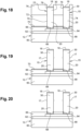
- THE figures 13 to 20 are partial and schematic sectional views of the structures obtained at successive stages of an embodiment of a method for manufacturing the chip 10 of the Figure 1 .
- the support 12 comprises a substrate 60, for example a semiconductor substrate, covered with an insulating layer 62.
- a conductive track 64 extends over the insulating layer 62.
- the conductive track 64 can be connected to regions of the semiconductor substrate 60 by conductive vias not shown.
- An insulating layer 66 extends over the conductive track 64 and over the insulating layer 66.
- a through opening 68 extends over the entire thickness of the insulating layer 66, each through opening 68 exposing a portion of the conductive track 64.
- the interconnection structure depends on the desired connections of the connection pillars. In the example illustrated in Figure 13 , both connecting pillars which are to be formed are connected to the conductive track 34.
- the substrate 60 is for example a substrate made of silicon, silicon carbide (SiC), III-V compounds, in particular gallium nitride (GaN), or diamond.
- the substrate 60 may have a single-layer or multi-layer structure, for example a structure of the silicon-on-insulator (SOI) type.
- the thickness of the substrate 60 is between 100 ⁇ m and 900 ⁇ m, and is for example equal to 200 ⁇ m.
- the insulating layer 62 is for example a layer of silicon oxide.
- the thickness of the insulating layer 62 is between 100 nm and 2 ⁇ m, and is for example equal to 200 nm.
- the conductive track 64 comprises for example a stack of metal layers.
- the metal track 64 can be produced by depositing full-plate metal layers and etching the metal layers to form the metal track 64.
- the thickness of the metal track 64 is between 200 nm and 2 ⁇ m, and is for example equal to 500 nm.
- the metal layers of the metal track are for example made of materials chosen from copper, a copper alloy, titanium, a titanium alloy, titanium nitride, platinum, and a platinum alloy.
- the metal layer 70 may comprise a layer of titanium or chromium, playing the role adhesion layer, and a copper layer acting as a primer layer for the subsequent formation of pillar 15.
- FIG. 15 represents the structure obtained after the formation of a first mask 72 in photosensitive resin on the metal layer 70 comprising through openings 74, each through opening 74 exposing the metal layer 70 in one of the openings 68.
- the through openings 74 can be produced by photolithography steps.
- the height of the first mask 72 is equal to the height H of the intermediate portion 20 of each pillar 15.
- FIG 16 represents the structure obtained after the formation of at least a part of the intermediate portion 20 of each pillar 15.
- the part of the intermediate portion 20 of each pillar 15 may not completely fill the corresponding opening 74.
- the material making up each pillar 15 may be deposited by electrodeposition.
- the free face 75 of the part of the intermediate portion 20 may be set back relative to the upper face of the first mask 72, as illustrated in figure 16 .
- FIG. 17 represents the structure obtained after the formation of a second mask 76 of photosensitive resin on the first mask 72 comprising through openings 78, each through opening 78 exposing one of the openings 74 of the first mask 72.
- the second mask 76 may be made of the same photosensitive resin as that used for the formation of the first mask 72, and the through openings 78 may be produced by photolithography steps.
- the height of the second resin mask 78 is greater than or equal to the height H' of the end portion 30 of each pillar 15.
- FIG. 18 represents the structure obtained after the formation of the remainder of the intermediate portion 20 of each pillar 15, the formation of the end portion 30 of each pillar 15, and the formation of the finishing layer 18 of each pillar 15.
- the material composing the trunk 16 of each pillar 15 can be deposited by electrodeposition.
- each pillar 15 obtained comprises the collar 17 located at the interface between the first mask 72 and the second mask 76.
- FIG. 20 represents the structure obtained after removing the metal layer 70 around the pillars 15.
- the formation of the trunk 16 of each pillar 15 comprises two electrodeposition deposition steps, the first deposition step comprising the partial filling of the openings 74 of the first mask 72 and the second deposition step comprising the end of the filling of the openings 74 of the first mask 72 and the total or partial filling of the openings 78 of the second mask 76.
- the formation of the trunk 16 of each pillar 15 comprises a single electrodeposition deposition step comprising the total filling of the openings 74 of the first mask 72 and the total or partial filling of the openings 78 of the second mask 76.
- Such a variant can be implemented when the form factor of the openings 74 and 78 is compatible with the electrodeposition method.
Landscapes
- Wire Bonding (AREA)
- Engineering & Computer Science (AREA)
- Manufacturing & Machinery (AREA)
- Furnace Charging Or Discharging (AREA)
- Connecting Device With Holders (AREA)
- Electric Connection Of Electric Components To Printed Circuits (AREA)
Abstract
Description
- La présente description concerne le domaine de la connexion électrique entre une puce électronique et un boîtier ou entre deux puces électroniques, et plus particulièrement des piliers de connexion de la puce électronique.
- Dans une puce électronique, les connexions sont faites par des réseaux d'interconnexion internes. Pour connecter une puce de circuit intégré à un élément extérieur, ces réseaux d'interconnexion sont connectés à des piliers, généralement situés sur une face de la puce. Ainsi, il est possible de mettre en contact les piliers avec des zones conductrices ou des pistes de connexion situées sur cet autre élément. L'élément peut correspondre à un substrat, également appelé boîtier notamment dans le domaine de l'électronique de puissance, par exemple un circuit imprimé. L'élément peut en outre correspondre à une autre puce électronique.
- Un exemple de procédé d'assemblage d'une puce électronique à une autre puce électronique ou un boîtier comprend la formation d'un bloc de pâte à fritter sur chaque pilier, le dépôt de la puce électronique sur l'autre puce électronique ou le boîtier, et le frittage de la pâte à fritter. Pour certaines applications, le frittage est mis en oeuvre à une température inférieure à 200 °C et sans l'exercice d'une pression sur la puce électronique. Pour de telles applications, l'étape de dépôt de la puce électronique sur l'autre puce électronique ou le boîtier est réalisée avant le séchage de la pâte à fritter.
- Un mode de réalisation pallie tout ou partie des inconvénients des puces électroniques comprenant des piliers de connexion connues.
- Un mode de réalisation prévoit une puce électronique comprenant un support et des piliers de connexion, chaque pilier de connexion comprenant un tronc comportant une portion d'extrémité et une portion intermédiaire reliant la portion d'extrémité au support et comprenant une collerette à la jonction entre la portion d'extrémité et la portion intermédiaire.
- Selon un mode de réalisation, la hauteur de la portion d'extrémité est comprise entre 10 µm et 100 µm.
- Selon un mode de réalisation, la hauteur de la portion intermédiaire est comprise entre 10 µm et 100 µm.
- Selon un mode de réalisation, l'écart entre la dimension latérale maximale de la collerette et la dimension latérale minimale de la portion d'extrémité est compris entre 1 µm et 7 µm.
- Selon un mode de réalisation, la portion d'extrémité comprend une face d'extrémité du côté opposé à la portion intermédiaire.
- Selon un mode de réalisation, la portion d'extrémité a une forme évasée du côté de la face d'extrémité.
- Selon un mode de réalisation, le pilier de connexion comprend une couche de finition recouvrant la face d'extrémité.
- Selon un mode de réalisation, le tronc est en cuivre.
- Un mode de réalisation prévoit également un procédé d'assemblage d'une puce électronique telle que définie précédemment à une autre puce électronique ou à un boîtier, comprenant la pénétration des piliers de connexion dans une couche de pâte à fritter au moins jusqu'à la collerette de chaque pilier de connexion, le retrait des piliers de connexion de la couche de pâte à fritter, un bloc de pâte à fritter restant accroché à chaque pilier de connexion, le dépôt de la puce électronique sur l'autre puce électronique ou sur le boîtier et le chauffage pour obtenir le frittage des blocs de pâte à fritter.
- Un mode de réalisation prévoit également un procédé de fabrication d'une puce électronique telle que définie précédemment, comprenant la formation d'un premier masque en résine photosensible comprenant, pour chaque pilier de connexion, une première ouverture traversante, le dépôt du matériau composant le tronc dans les premières ouvertures traversantes, la formation d'un deuxième masque en résine photosensible comprenant une deuxième ouverture traversante dans le prolongement de chaque première ouverture traversante, et le dépôt du matériau composant le tronc dans les deuxièmes ouvertures traversantes.
- Ces caractéristiques et avantages, ainsi que d'autres, seront exposés en détail dans la description suivante de modes de réalisation particuliers faite à titre non limitatif en relation avec les figures jointes parmi lesquelles :
- la
figure 1 représente, schématiquement, un mode de réalisation d'un pilier de connexion d'une puce ; - la
figure 2 , lafigure 3 , et lafigure 4 représentent chacune, schématiquement, un autre mode de réalisation d'un pilier de connexion ; - la
figure 5 et lafigure 6 sont chacune une image obtenue par microscopie électronique à balayage du pilier de connexion de lafigure 1 ; - la
figure 7 , lafigure 8 , lafigure 9 , et lafigure 10 représentent des structures obtenues à des étapes successives d'un mode de réalisation d'un procédé d'assemblage de la puce de lafigure 1 à une autre puce ou à un boîtier ; - la
figure 11 est une image obtenue par microscopie électronique à balayage du pilier de connexion de lafigure 1 à l'étape du procédé d'assemblage illustré enfigure 9 ; - la
figure 12 est une image obtenue par microscopie électronique à balayage d'une coupe de la structure obtenue à l'étape du procédé d'assemblage illustré enfigure 10 ; et - la
figure 13 , lafigure 14 , lafigure 15 , lafigure 16 , lafigure 17 , lafigure 18 , lafigure 19 , et lafigure 20 représentent des structures obtenues à des étapes successives d'un mode de réalisation d'un procédé de fabrication de la puce de lafigure 1 . - De mêmes éléments ont été désignés par de mêmes références dans les différentes figures. En particulier, les éléments structurels et/ou fonctionnels communs aux différents modes de réalisation peuvent présenter les mêmes références et peuvent disposer de propriétés structurelles, dimensionnelles et matérielles identiques.
- Par souci de clarté, seuls les étapes et éléments utiles à la compréhension des modes de réalisation décrits ont été représentés et sont détaillés. En particulier, les divers composants des puces, ainsi que les connexions internes des puces, ne sont pas détaillés.
- Sauf précision contraire, lorsque l'on fait référence à deux éléments connectés entre eux, cela signifie directement connectés sans éléments intermédiaires autres que des conducteurs, et lorsque l'on fait référence à deux éléments reliés (en anglais "coupled") entre eux, cela signifie que ces deux éléments peuvent être connectés ou être reliés par l'intermédiaire d'un ou plusieurs autres éléments. En outre, on considère ici que les termes "isolant" et "conducteur" signifient respectivement "isolant électriquement" et "conducteur électriquement".
- Dans la description qui suit, lorsque l'on fait référence à des qualificatifs de position absolue, tels que les termes "avant", "arrière", "haut", "bas", "gauche", "droite", etc., ou relative, tels que les termes "dessus", "dessous", "supérieur", "inférieur", etc., ou à des qualificatifs d'orientation, tels que les termes "horizontal", "vertical", etc., il est fait référence sauf précision contraire à l'orientation des figures ou à un circuit électronique dans une position normale d'utilisation.
- Sauf précision contraire, les expressions "environ", "approximativement", "sensiblement", et "de l'ordre de" signifient à 10 % près, de préférence à 5 % près.
- La
figure 1 est une vue de côté, partielle et schématique, d'un mode de réalisation d'une puce électronique 10 que l'on souhaite connecter à un boîtier ou une autre puce électronique, non représentée. La puce 10 comprend des piliers de connexion 15, également appelés plots de connexion, en un matériau conducteur. Bien que deux piliers de connexion 15 soient représentés enfigure 1 , la puce 10 comprend autant de piliers de connexion 15 que de connexions à faire (selon l'application visée, seuls deux, plusieurs dizaines, voire plusieurs milliers de piliers de connexion 15 peuvent être présents) . La puce 10 comprend par exemple un support 12 ayant une face 13 sur laquelle sont réalisées les connexions électriques avec l'extérieur de la puce 10. A titre d'exemple, le support 12 comprend un substrat, par exemple en silicium, recouvert d'une structure d'interconnexion comprenant des éléments conducteurs non représentés, par exemple des vias et des métallisations. Chaque pilier de connexion 15 est par exemple connecté électriquement à de tels éléments conducteurs. - Chaque pilier 15 comprend un tronc 16 ayant une portion intermédiaire 20 et une portion d'extrémité 30. La portion intermédiaire 20 est située entre le support 10 et la portion d'extrémité 30. Le pilier 15 comprend une collerette 17 à la jonction entre la portion intermédiaire 20 et la portion d'extrémité 30. La portion intermédiaire 20 comprend une base 22, une face de liaison 24 opposée à la base 22, et une paroi latérale 26 reliant la base 22 à la face de liaison 24. La portion d'extrémité 30 comprend une face de liaison 32, une face d'extrémité 34 opposée à la face de liaison 32, et une paroi latérale 36 reliant la face de liaison 32 à la face d'extrémité 34. La base 22 de la portion intermédiaire 20 est au contact physique direct du support 12. La face de liaison 24 de la portion intermédiaire 20 est confondue avec la face de liaison 32 de la portion d'extrémité 30. Selon un mode de réalisation, la paroi latérale 36 de portion d'extrémité 30 comprend en outre une partie évasée 38 du côté de la face supérieure 32. Selon un mode de réalisation, la paroi latérale 26 de portion intermédiaire 20 comprend en outre une partie évasée 28 du côté de la base 22.
- La paroi latérale 26 de la portion intermédiaire 20 est contenue entre un cylindre interne à base circulaire Cint d'axe Δ et un cylindre externe Cext à base circulaire d'axe Δ, et est au contact du cylindre interne Cint et du cylindre externe Cext. Selon un mode de réalisation, Selon un mode de réalisation, la face de liaison 24 de la portion intermédiaire 20 est sensiblement perpendiculaire à l'axe Δ. La hauteur H de la portion intermédiaire 20, mesurée selon l'axe Δ, est comprise entre 10 µm et 100 um, et est de préférence égale à environ 50 µm. Le diamètre du cylindre interne Cint est compris entre 10 µm et 3 mm, et est de préférence égale à environ 50 µm. L'écart entre le rayon du cylindre externe Cext et le rayon du cylindre interne Cint est compris entre 1 µm et 100 µm, de préférence entre 1 µm et 7 µm. Selon un mode de réalisation, le pas entre les axes Δ de piliers 15 adjacents est compris entre 20 µm et 7 mm, et est de préférence égal à environ 100 µm. Selon un mode de réalisation, excepté à proximité de la base 22 et de la face de liaison 24, la portion intermédiaire 20 a pour l'essentiel une forme cylindrique à base circulaire.
- La paroi latérale 36 de la portion d'extrémité 30 est contenue entre un cylindre interne Cint' à base circulaire d'axe Δ' et un cylindre externe Cext' à base circulaire d'axe Δ', et est au contact du cylindre interne Cint' et du cylindre externe Cext'. L'axe Δ est parallèle à l'axe Δ'. Selon un mode de réalisation, l'axe Δ' est confondu avec l'axe Δ. Toutefois, l'axe Δ' peut être décalé par rapport à l'axe Δ. Le décalage entre l'axe Δ' et l'axe Δ peut être compris entre 0 µm et 6 µm. Selon un mode de réalisation, la face de liaison 32 de la portion d'extrémité 30 est sensiblement perpendiculaire à l'axe Δ. Selon un mode de réalisation, la face d'extrémité 34 de la portion d'extrémité 30 est sensiblement perpendiculaire à l'axe Δ. La hauteur H' de la portion d'extrémité 30 mesurée selon l'axe Δ' est comprise entre 10 µm et 100 um, de préférence entre 10 µm et 40 µm, et est par exemple égale à environ 20 µm. L'écart entre le rayon du cylindre externe Cext' et le rayon du cylindre interne Cint' est compris entre 1 µm et 7 µm, de préférence entre 1 µm et 4 µm. Selon un mode de réalisation, excepté à proximité de la face de liaison 32 et de la face d'extrémité 34, la portion d'extrémité 30 a pour l'essentiel une forme cylindrique à base circulaire.
- Le tronc 16 est en métal, par exemple en cuivre, en nickel, en argent, en or, ou en un alliage de ces métaux.
- Selon un mode de réalisation, le pilier 15 comprend, en outre, une couche de finition 18 recouvrant la face d'extrémité 34 de la portion d'extrémité 30 du tronc 16. L'épaisseur de la couche de finition 18 est comprise entre 10 nm et 1000 nm. La couche de finition 18 est en un matériau conducteur qui améliore l'adhésion de pâte à fritter. La couche de finition 18 est par exemple en métal, notamment en or ou en argent, et comprend éventuellement une ou des couches d'accroche et/ou une ou des couches barrière, comprenant par exemple du platine (Pt), du palladium (Pd), du nickel (Ni), du titane (Ti), du chrome (Cr), et/ou du tantale (Ta), entre le matériau du tronc 16 et le matériau de la pâte à fritter qui est déposée par la suite sur le pilier 15. La couche de finition 18 permet en outre d'éviter une oxydation de la face d'extrémité 34 du pilier 15 dans le cas où le procédé d'assemblage n'est pas réalisé sous atmosphère neutre ou réductrice.
- La
figure 2 est une vue de côté, partielle et schématique, d'un autre mode de réalisation de la puce 10. Chaque pilier 15 de la puce 10 représentée enfigure 2 comprend l'ensemble des éléments du pilier 15 de la puce 10 représentée enfigure 1 à la différence que la portion d'extrémité 30 du tronc 16 ne comprend pas de partie évasée 38 du côté de la face supérieure 34. - La
figure 3 est une vue de côté, partielle et schématique, d'un autre mode de réalisation de la puce 10. Chaque pilier 15 de la puce 10 représentée enfigure 3 comprend l'ensemble des éléments du pilier 15 de la puce 10 représentée enfigure 1 à la différence que la couche de finition 18 n'est pas présente. - La
figure 4 est une vue de côté, partielle et schématique, d'un autre mode de réalisation de la puce 10. Chaque pilier 15 de la puce 10 représentée enfigure 4 comprend l'ensemble des éléments du pilier 15 de la puce 10 représentée enfigure 2 à la différence que la couche de finition 18 n'est pas présente. - La
figure 5 est une image obtenue par microscopie électronique à balayage selon une vue en perspective d'un pilier 15 selon le mode de réalisation décrit précédemment en relation avec lafigure 1 . - La
figure 6 est une image obtenue par microscopie électronique à balayage du pilier 15 de lafigure 5 vu selon l'axe Δ du côté de la couche d'accrochage 18. Dans cet exemple, l'axe Δ est décalé par rapport à l'axe Δ'. - Les
figures 7 à 10 comprennent chacune une vue en coupe en partie gauche et une vue de côté en partie droite de la structure obtenue à des étapes successives d'un mode de réalisation d'un procédé d'assemblage de la puce 10 à une autre puce ou à un boîtier. - La
figure 7 illustre la structure obtenue après la formation d'une couche 50 de pâte à fritter dans une cavité 52. L'épaisseur de la couche 50 de pâte est supérieure à la hauteur H' de la portion d'extrémité 30 du pilier 15. L'épaisseur de la couche 50 de pâte est comprise entre 20 µm et 200 µm, et est par exemple égale à environ 50 µm. - La puce 10 est placée au-dessus de la couche 50 de pâte par rapport à une direction verticale et à distance de la couche 50 de pâte. La couche de finition 18 de chaque pilier 15 est orientée du côté de la couche 50 de pâte. La viscosité dynamique de la couche 50 de pâte est comprise entre 20 Pa.s et 60 Pa.s. La thixotropie de la couche 50 de pâte est comprise entre 3 et 7. La couche 50 de pâte est en un matériau susceptible d'être fritté. La couche 50 de pâte comprend notamment une charge active comprenant des particules d'un matériau métallique, par exemple de l'argent, du cuivre, ou un alliage d'argent et de cuivre. La charge active peut en outre comprendre de l'or et d'autres additifs, par exemple des polymères et/ou des céramiques, ne participant pas au frittage mais facilitant les procédés de mise en oeuvre de la pâte à fritter. La proportion de la charge active dans la couche 50 de pâte est comprise de 60 % à 97 % en masse.
- La
figure 8 illustre la structure obtenue après l'enfoncement de la puce 10 dans la couche 50 de pâte jusqu'à ce qu'au moins la totalité de la portion d'extrémité 30 de chaque pilier 15 ait pénétré dans la couche 50 de pâte. Selon un mode de réalisation, la puce 10 est déplacée par rapport à la couche 50 de pâte au moyen d'un outil de manipulation, non représenté, par exemple selon un déplacement vertical (flèche F1). Selon un mode de réalisation, la puce 10 est mise en déplacement à une vitesse initiale donnée. Selon un mode de réalisation, un effort de résistance à la pénétration de la puce 10 dans la couche 50 de pâte est mesuré et le déplacement de la puce 10 est arrêté lorsque l'effort de résistance dépasse un seuil. - La
figure 9 illustre la structure obtenue après le retrait (flèche F2) de la puce 10 hors de la couche 50 de pâte jusqu'à ce que chaque pilier 15 soit en totalité en dehors de la couche 50 de pâte. Un bloc 52 de pâte reste accroché à chaque pilier 15. La couche de finition 18 est en matériau qui favorise l'adhésion du bloc 52 de pâte. Les inventeurs ont mis en évidence que la présence de la collerette 17 fait que le volume du bloc 52 de pâte qui reste accroché au pilier 15 est plus important par rapport au cas où la collerette 17 n'est pas présente. L'épaisseur minimale du bloc 52 de pâte entre chaque pilier 15 et l'autre puce/le boîtier 54 est supérieure à 4 µm, de préférence comprise entre 7 µm et 15 µm. Une épaisseur minimale élevée peut être obtenue en raison du volume important du bloc 52 de pâte qui est emporté par chaque pilier 15. - La
figure 10 illustre la structure obtenue après le dépôt de la puce 10 sur une autre puce ou un boîtier 54 de telle manière que chaque pilier 15 soit en regard d'une piste conductrice 55 de l'autre puce ou du boîtier 54, le bloc 52 de pâte contactant la piste conductrice 55. Selon un mode de réalisation, le puce 10 est posée sur l'autre puce/le boîtier 54 (flèche F3), ce qui entraîne une déformation des blocs 52 de pâte seulement sous l'action du poids de la puce 10. Selon un mode de réalisation, la puce 10 est déplacée vers l'autre puce/le boîtier 54 par un outil de manipulation, non représenté, jusqu'à ce qu'un critère soit atteint, par exemple jusqu'à ce que la distance entre le support 12 de la puce 10 et l'autre puce/le boîtier 54 atteigne une distance donnée, ou jusqu'à ce que l'effort de résistance au déplacement de la puce 10 dépasse un seuil. La déformation des blocs 52 de pâte est alors due également à l'action exercée par l'outil de manipulation sur la puce 10. L'épaisseur minimale du bloc 52 de pâte entre chaque pilier 15 et l'autre puce/le boîtier 54 après le retrait de la puce 10 hors de la couche 50 de pâte permet d'assurer que de la pâtre à fritter reste présente entre chaque pilier 15 et la piste conductrice 55 malgré une éventuelle inhomogénéité de hauteur des piliers présents sur la puce 10 et/ou une éventuelle courbure de la puce 10. - Le procédé se poursuit avec une étape de chauffage entraînant le frittage du bloc 52 de pâte et l'adhésion de la puce 10 à la puce ou au boîtier 54, par exemple à une température inférieure à 200 °C. Selon un mode de réalisation, pendant l'étape de chauffage, il n'y a pas de pression exercée sur la puce 10 ou seulement une pression inférieure à 1 MPa. Selon un mode de réalisation, la température de chauffage est comprise entre 130 °C et 300 °C, de préférence entre 150 °C et 250 °C.
- La
figure 11 est une image obtenue par microscopie électronique à balayage selon une vue en perspective d'un pilier 15 à l'étape décrite précédemment en relation avec lafigure 9 , c'est-à-dire après le retrait de la puce 10 hors de la couche 50 de pâte. La portion intermédiaire 20 est située en bas de l'image. Le bloc 52 de pâte recouvre complètement la portion d'extrémité du pilier 15. - La
figure 12 est une image obtenue par microscopie électronique à balayage d'une coupe d'un pilier 15 à l'étape décrite précédemment en relation avec lafigure 10 , c'est-à-dire après le dépôt de la puce 10 sur l'autre puce ou le boîtier 54. - Les
figures 13 à 20 sont des vues en coupe, partielles et schématiques, des structures obtenues à des étapes successives d'un mode de réalisation d'un procédé de fabrication de la puce 10 de lafigure 1 . - La
figure 13 représente la structure obtenue après la formation d'une structure d'interconnexion du support 12. Selon un mode de réalisation, le support 12 comprend un substrat 60, par exemple un substrat semiconducteur, recouvert d'une couche isolante 62. Une piste conductrice 64 s'étend sur la couche isolante 62. La piste conductrice 64 peut être connectée à des régions du substrat semiconducteur 60 par des vias conducteurs non représentés. Une couche isolante 66 s'étend sur la piste conductrice 64 et sur la couche isolante 66. Pour chaque pilier de connexion à réaliser, une ouverture traversante 68 s'étend sur toute l'épaisseur de la couche isolante 66, chaque ouverture traversante 68 exposant une partie de la piste conductrice 64. La structure d'interconnexion dépend des connexions souhaitées des piliers de connexion. Dans l'exemple illustré enfigure 13 , les deux piliers de connexion qui vont être formés sont connectés à la piste conductrice 34. - Le substrat 60 est par exemple un substrat en silicium, en carbure de silicium (SiC), en composes III-V, notamment le nitrure de gallium (GaN), en diamant. Le substrat 60 peut avoir une structure monocouche ou multicouches, par exemple une structure du type silicium sur isolant (SOI, sigle anglais pour Silicon On Insulator). Selon un mode de réalisation, l'épaisseur du substrat 60 est comprise entre 100 µm et 900 µm, et est par exemple égale à 200 µm. La couche isolante 62 est par exemple une couche en oxyde de silicium. Selon un mode de réalisation, l'épaisseur de la couche isolante 62 est comprise entre 100 nm et 2 µm, et est par exemple égale à 200 nm. La piste conductrice 64 comprend par exemple un empilement de couches métalliques. Selon un mode de réalisation, la piste métallique 64 peut être réalisée par le dépôt de couches métalliques pleine plaque et la gravure des couches métalliques pour former la piste métallique 64. Selon un mode de réalisation, l'épaisseur de la piste métallique 64 est comprise entre 200 nm et 2 µm, et est par exemple égale à 500 nm. Les couches métalliques de la piste métallique sont par exemple en des matériaux choisis parmi le cuivre, un alliage de cuivre, le titane, un alliage de titane, le nitrure de titane, le platine, et un alliage de platine.
- La
figure 14 représente la structure obtenue après la formation d'une couche métallique 70 sur la totalité de la structure obtenue à l'étape précédente. En particulier, la couche métallique 70 s'étend dans le fond de chaque ouverture 68 au contact de la piste métallique 64. Selon un mode de réalisation, l'épaisseur de la couche métallique 70 est comprise entre 10 nm et 1 µm. La couche métallique 70 peut comprendre une couche de titane ou de chrome, jouant le rôle de couche d'adhérence, et une couche de cuivre jouant le rôle de couche d'amorce pour la formation ultérieure du pilier 15. - La
figure 15 représente la structure obtenue après la formation d'un premier masque 72 en résine photosensible sur la couche métallique 70 comprenant des ouvertures traversantes 74, chaque ouverture traversante 74 exposant la couche métallique 70 dans l'une des ouvertures 68. Les ouvertures traversantes 74 peuvent être réalisées par des étapes de photolithographie. La hauteur du premier masque 72 est égale à la hauteur H de la portion intermédiaire 20 de chaque pilier 15. - La
figure 16 représente la structure obtenue après la formation d'au moins une partie de la portion intermédiaire 20 de chaque pilier 15. Selon un mode de réalisation, la partie de la portion intermédiaire 20 de chaque pilier 15 peut ne remplir complètement l'ouverture 74 correspondante. Le matériau composant chaque pilier 15 peut être déposé par électrodéposition. La face libre 75 de la partie de la portion intermédiaire 20 peut être en retrait par rapport à la face supérieure du premier masque 72, comme cela est illustré enfigure 16 . - La
figure 17 représente la structure obtenue après la formation d'un deuxième masque 76 en résine photosensible sur le premier masque 72 comprenant des ouvertures traversantes 78, chaque ouverture traversante 78 exposant l'une des ouvertures 74 du premier masque 72. Le deuxième masque 76 peut être en la même résine photosensible que celle utilisée pour la formation du premier masque 72, et les ouvertures traversantes 78 peuvent être réalisées par des étapes de photolithographie. La hauteur du deuxième masque de résine 78 est supérieure ou égale à la hauteur H' de la portion d'extrémité 30 de chaque pilier 15. - La
figure 18 représente la structure obtenue après la formation du reste de la portion intermédiaire 20 de chaque pilier 15, la formation de la portion d'extrémité 30 de chaque pilier 15, et la formation de la couche de finition 18 de chaque pilier 15. Le matériau composant le tronc 16 de chaque pilier 15 peut être déposé par électrodéposition. - La
figure 19 représente la structure obtenue après le retrait du deuxième masque 76 et le retrait du premier masque 72. Cela peut être réaliser par dissolution de la résine dans un solvant ou par une étape de gravure à sec. Les inventeurs ont mis en évidence que chaque pilier 15 obtenu comprend la collerette 17 située à l'interface entre le premier masque 72 et le deuxième masque 76. - La
figure 20 représente la structure obtenue après le retrait de la couche métallique 70 autour des piliers 15. - Dans le mode de réalisation décrit précédemment en relation avec les
figures 13 à 20 , la formation du tronc 16 de chaque pilier 15 comprend deux étapes de dépôt par électrodéposition, la première étape de dépôt comprenant le remplissage partiel des ouvertures 74 du premier masque 72 et la deuxième étape de dépôt comprenant la fin du remplissage des ouvertures 74 du premier masque 72 et le remplissage total ou partiel des ouvertures 78 du deuxième masque 76. A titre de variante, la formation du tronc 16 de chaque pilier 15 comprend une seule étape de dépôt par électrodéposition comprenant le remplissage total des ouvertures 74 du premier masque 72 et le remplissage total ou partiel des ouvertures 78 du deuxième masque 76. Une telle variante peut être mise en oeuvre lorsque le facteur de forme des ouvertures 74 et 78 est compatible avec le procédé d'électrodéposition. - Divers modes de réalisation et variantes ont été décrits. La personne du métier comprendra que certaines caractéristiques de ces divers modes de réalisation et variantes pourraient être combinées, et d'autres variantes apparaîtront à la personne du métier. Enfin, la mise en oeuvre pratique des modes de réalisation et variantes décrits est à la portée de la personne du métier à partir des indications fonctionnelles données ci-dessus.
Claims (11)
- Procédé de fabrication d'une puce électronique (10) comprenant un support (12) et des piliers de connexion (15), chaque pilier de connexion (15) comprenant un tronc (16) comportant une portion d'extrémité (30) et une portion intermédiaire (20) reliant la portion d'extrémité (30) au support (12) et comprenant une collerette (17) à la jonction entre la portion d'extrémité (30) et la portion intermédiaire (20), le procédé comprenant la formation d'un premier masque (72) en résine photosensible comprenant, pour chaque pilier de connexion (15), une première ouverture traversante (74), le dépôt du matériau composant le tronc (16) dans les premières ouvertures traversantes (74), la formation d'un deuxième masque (76) en résine photosensible comprenant une deuxième ouverture traversante (78) dans le prolongement de chaque première ouverture traversante (74), et le dépôt du matériau composant le tronc (16) dans les deuxièmes ouvertures traversantes (78) .
- Procédé de fabrication selon la revendication 1, dans lequel la hauteur (H') de la portion d'extrémité (30) est comprise entre 10 µm et 100 µm.
- Procédé de fabrication selon la revendication 1 ou 2, dans lequel la hauteur (H) de la portion intermédiaire (20) est comprise entre 10 µm et 100 µm.
- Procédé de fabrication selon l'une quelconque des revendications 1 à 3, dans lequel l'écart entre la dimension latérale maximale de la collerette (17) et la dimension latérale minimale de la portion d'extrémité (30) est compris entre 1 µm et 7 µm.
- Procédé de fabrication selon l'une quelconque des revendications 1 à 4, dans lequel la portion d'extrémité (30) comprend une face d'extrémité (34) du côté opposé à la portion intermédiaire (20).
- Procédé de fabrication selon la revendication 5, dans lequel la portion d'extrémité (30) a une forme évasée (38) du côté de la face d'extrémité (34).
- Procédé de fabrication selon la revendication 5 ou 6, dans lequel le pilier de connexion (15) comprend une couche de finition (18) recouvrant la face d'extrémité (34).
- Procédé de fabrication selon l'une quelconque des revendications 1 à 7, dans lequel le tronc (16) est en cuivre.
- Procédé d'assemblage d'une puce électronique (10) fabriquée selon le procédé de fabrication selon l'une quelconque des revendications 1 à 8 à une autre puce électronique ou à un boîtier (54), comprenant la pénétration des piliers de connexion (15) dans une couche (50) de pâte à fritter au moins jusqu'à la collerette (17) de chaque pilier de connexion (15), le retrait des piliers de connexion (15) de la couche (50) de pâte à fritter, un bloc (52) de pâte à fritter restant accroché à chaque pilier de connexion (15) au moins sur la hauteur (H') de la portion d'extrémité (30), de préférence sur une hauteur égale à 50 µm, le dépôt de la puce électronique (10) sur l'autre puce électronique ou sur le boîtier (54) et le chauffage pour obtenir le frittage des blocs (52) de pâte à fritter.
- Procédé d'assemblage selon la revendication 9, dans lequel, pendant le chauffage pour obtenir le frittage des blocs (52) de pâte à fritter, il n'y a pas de pression exercée sur la puce électronique (10).
- Procédé d'assemblage selon la revendication 9 ou 10, dans lequel la quantité de pâte à fritter après collage, entre chaque pilier de connexion (15) et l'autre puce électronique ou le boîtier (54), est supérieure à 4 µm, de préférence comprise entre 7 µm et 15 µm.
Applications Claiming Priority (1)
| Application Number | Priority Date | Filing Date | Title |
|---|---|---|---|
| FR2309488A FR3152914B1 (fr) | 2023-09-08 | 2023-09-08 | Puce électronique comprenant des piliers de connexion pour un assemblage par frittage |
Publications (2)
| Publication Number | Publication Date |
|---|---|
| EP4521449A1 true EP4521449A1 (fr) | 2025-03-12 |
| EP4521449B1 EP4521449B1 (fr) | 2025-11-05 |
Family
ID=89157911
Family Applications (1)
| Application Number | Title | Priority Date | Filing Date |
|---|---|---|---|
| EP24198761.9A Active EP4521449B1 (fr) | 2023-09-08 | 2024-09-05 | Procédé de fabrication d'une puce électronique comprenant des piliers de connexion pour un assemblage par frittage |
Country Status (3)
| Country | Link |
|---|---|
| US (1) | US20250087610A1 (fr) |
| EP (1) | EP4521449B1 (fr) |
| FR (1) | FR3152914B1 (fr) |
Citations (4)
| Publication number | Priority date | Publication date | Assignee | Title |
|---|---|---|---|---|
| JP2007335464A (ja) * | 2006-06-12 | 2007-12-27 | Nec Corp | 金属ポストを有する配線基板、半導体装置、半導体装置モジュール及びそれらの製造方法 |
| US20100148374A1 (en) * | 2008-12-17 | 2010-06-17 | Texas Instruments Incorporated | Method for low stress flip-chip assembly of fine-pitch semiconductor devices |
| US8723318B2 (en) * | 2010-07-08 | 2014-05-13 | Tessera, Inc. | Microelectronic packages with dual or multiple-etched flip-chip connectors |
| US11094655B2 (en) * | 2019-06-13 | 2021-08-17 | Taiwan Semiconductor Manufacturing Co., Ltd. | Semiconductor structure and method for forming the same |
-
2023
- 2023-09-08 FR FR2309488A patent/FR3152914B1/fr active Active
-
2024
- 2024-09-05 US US18/825,283 patent/US20250087610A1/en active Pending
- 2024-09-05 EP EP24198761.9A patent/EP4521449B1/fr active Active
Patent Citations (4)
| Publication number | Priority date | Publication date | Assignee | Title |
|---|---|---|---|---|
| JP2007335464A (ja) * | 2006-06-12 | 2007-12-27 | Nec Corp | 金属ポストを有する配線基板、半導体装置、半導体装置モジュール及びそれらの製造方法 |
| US20100148374A1 (en) * | 2008-12-17 | 2010-06-17 | Texas Instruments Incorporated | Method for low stress flip-chip assembly of fine-pitch semiconductor devices |
| US8723318B2 (en) * | 2010-07-08 | 2014-05-13 | Tessera, Inc. | Microelectronic packages with dual or multiple-etched flip-chip connectors |
| US11094655B2 (en) * | 2019-06-13 | 2021-08-17 | Taiwan Semiconductor Manufacturing Co., Ltd. | Semiconductor structure and method for forming the same |
Also Published As
| Publication number | Publication date |
|---|---|
| EP4521449B1 (fr) | 2025-11-05 |
| US20250087610A1 (en) | 2025-03-13 |
| FR3152914B1 (fr) | 2025-09-19 |
| FR3152914A1 (fr) | 2025-03-14 |
Similar Documents
| Publication | Publication Date | Title |
|---|---|---|
| EP2175485B1 (fr) | Connexion par emboitement de deux inserts soudés et sa méthode de fabrication | |
| EP3769339B1 (fr) | Dispositif d'affichage emissif a led et procede de fabrication d'un tel dispositif | |
| EP2727144B1 (fr) | Procédé d'hybridation d'un composant muni d'inserts creux | |
| EP2192612B1 (fr) | Procédé pour empiler et interconnecter des circuits intégrés | |
| EP2255383B1 (fr) | Composant de connexion muni d'inserts creux et son procede de realisation | |
| EP4002441A2 (fr) | Circuit electronique pour un collage moleculaire hybride | |
| FR2980036A1 (fr) | Procede de realisation d'une structure integree tridimensionnelle et structure correspondante | |
| EP3913657A2 (fr) | Procédé de traitement d'un circuit électronique pour un collage moléculaire hybride | |
| EP4521449B1 (fr) | Procédé de fabrication d'une puce électronique comprenant des piliers de connexion pour un assemblage par frittage | |
| EP2791969B1 (fr) | Formation d'une connexion electrique du type via | |
| FR2766294A1 (fr) | Procede de fabrication d'une capacite metal-metal au sein d'un circuit integre, et circuit integre correspondant | |
| EP3591724A1 (fr) | Procede de realisation d'un dispositif transducteur piezoelectrique | |
| FR3093592A1 (fr) | Circuit intégré comportant un condensateur tridimensionnel | |
| WO2018033689A1 (fr) | Procédé de connection intercomposants à densité optimisée | |
| EP4528806B1 (fr) | Puce electronique comprenant des piliers de connexion | |
| EP1180790B1 (fr) | Fabrication de condensateurs à armatures métalliques | |
| EP4012735A1 (fr) | Procédé de fabrication d'un condensateur | |
| FR2901635A1 (fr) | Dispositif de connexion tridimensionnel dans un substrat | |
| EP4571825A1 (fr) | Procede de fabrication de composants electroniques a flancs mouillables | |
| EP3886159A1 (fr) | Puce d'interconnexion | |
| FR3168129A1 (fr) | Circuit électronique comprenant des plots de connexion | |
| EP4350761A1 (fr) | Puce electronique comportant une metallisation de type ubm | |
| EP3467856B1 (fr) | Procédés de fabrication d'une traversée hermétique et isolante pour un boitier, notamment en titane, d'un dispositif électronique | |
| FR3166264A1 (fr) | Procédé d'assemblage d'un composant électroacoustique à un circuit électronique par soudure par refusion | |
| EP4435835A1 (fr) | Procédé de fabrication d'une pluralité de composants électroniques |
Legal Events
| Date | Code | Title | Description |
|---|---|---|---|
| PUAI | Public reference made under article 153(3) epc to a published international application that has entered the european phase |
Free format text: ORIGINAL CODE: 0009012 |
|
| STAA | Information on the status of an ep patent application or granted ep patent |
Free format text: STATUS: REQUEST FOR EXAMINATION WAS MADE |
|
| 17P | Request for examination filed |
Effective date: 20240905 |
|
| AK | Designated contracting states |
Kind code of ref document: A1 Designated state(s): AL AT BE BG CH CY CZ DE DK EE ES FI FR GB GR HR HU IE IS IT LI LT LU LV MC ME MK MT NL NO PL PT RO RS SE SI SK SM TR |
|
| GRAP | Despatch of communication of intention to grant a patent |
Free format text: ORIGINAL CODE: EPIDOSNIGR1 |
|
| STAA | Information on the status of an ep patent application or granted ep patent |
Free format text: STATUS: GRANT OF PATENT IS INTENDED |
|
| INTG | Intention to grant announced |
Effective date: 20250613 |
|
| GRAS | Grant fee paid |
Free format text: ORIGINAL CODE: EPIDOSNIGR3 |
|
| GRAA | (expected) grant |
Free format text: ORIGINAL CODE: 0009210 |
|
| STAA | Information on the status of an ep patent application or granted ep patent |
Free format text: STATUS: THE PATENT HAS BEEN GRANTED |
|
| AK | Designated contracting states |
Kind code of ref document: B1 Designated state(s): AL AT BE BG CH CY CZ DE DK EE ES FI FR GB GR HR HU IE IS IT LI LT LU LV MC ME MK MT NL NO PL PT RO RS SE SI SK SM TR |
|
| REG | Reference to a national code |
Ref country code: CH Ref legal event code: F10 Free format text: ST27 STATUS EVENT CODE: U-0-0-F10-F00 (AS PROVIDED BY THE NATIONAL OFFICE) Effective date: 20251105 Ref country code: GB Ref legal event code: FG4D Free format text: NOT ENGLISH |
|
| REG | Reference to a national code |
Ref country code: DE Ref legal event code: R096 Ref document number: 602024001179 Country of ref document: DE |
|
| REG | Reference to a national code |
Ref country code: DE Ref legal event code: R079 Ref document number: 602024001179 Country of ref document: DE Free format text: PREVIOUS MAIN CLASS: H01L0021600000 Ipc: H10W0070010000 |
|
| REG | Reference to a national code |
Ref country code: IE Ref legal event code: FG4D Free format text: LANGUAGE OF EP DOCUMENT: FRENCH |
|
| REG | Reference to a national code |
Ref country code: NL Ref legal event code: MP Effective date: 20251105 |
|
| PG25 | Lapsed in a contracting state [announced via postgrant information from national office to epo] |
Ref country code: ES Free format text: LAPSE BECAUSE OF FAILURE TO SUBMIT A TRANSLATION OF THE DESCRIPTION OR TO PAY THE FEE WITHIN THE PRESCRIBED TIME-LIMIT Effective date: 20251105 |
|
| REG | Reference to a national code |
Ref country code: LT Ref legal event code: MG9D |
|
| PG25 | Lapsed in a contracting state [announced via postgrant information from national office to epo] |
Ref country code: NO Free format text: LAPSE BECAUSE OF FAILURE TO SUBMIT A TRANSLATION OF THE DESCRIPTION OR TO PAY THE FEE WITHIN THE PRESCRIBED TIME-LIMIT Effective date: 20260205 |
|
| PG25 | Lapsed in a contracting state [announced via postgrant information from national office to epo] |
Ref country code: HR Free format text: LAPSE BECAUSE OF FAILURE TO SUBMIT A TRANSLATION OF THE DESCRIPTION OR TO PAY THE FEE WITHIN THE PRESCRIBED TIME-LIMIT Effective date: 20251105 Ref country code: FI Free format text: LAPSE BECAUSE OF FAILURE TO SUBMIT A TRANSLATION OF THE DESCRIPTION OR TO PAY THE FEE WITHIN THE PRESCRIBED TIME-LIMIT Effective date: 20251105 Ref country code: AT Free format text: LAPSE BECAUSE OF FAILURE TO SUBMIT A TRANSLATION OF THE DESCRIPTION OR TO PAY THE FEE WITHIN THE PRESCRIBED TIME-LIMIT Effective date: 20251105 |
|
| REG | Reference to a national code |
Ref country code: AT Ref legal event code: MK05 Ref document number: 1855353 Country of ref document: AT Kind code of ref document: T Effective date: 20251105 |
|
| PG25 | Lapsed in a contracting state [announced via postgrant information from national office to epo] |
Ref country code: NL Free format text: LAPSE BECAUSE OF FAILURE TO SUBMIT A TRANSLATION OF THE DESCRIPTION OR TO PAY THE FEE WITHIN THE PRESCRIBED TIME-LIMIT Effective date: 20251105 |
|
| PG25 | Lapsed in a contracting state [announced via postgrant information from national office to epo] |
Ref country code: RS Free format text: LAPSE BECAUSE OF FAILURE TO SUBMIT A TRANSLATION OF THE DESCRIPTION OR TO PAY THE FEE WITHIN THE PRESCRIBED TIME-LIMIT Effective date: 20260205 |
|
| PG25 | Lapsed in a contracting state [announced via postgrant information from national office to epo] |
Ref country code: IS Free format text: LAPSE BECAUSE OF FAILURE TO SUBMIT A TRANSLATION OF THE DESCRIPTION OR TO PAY THE FEE WITHIN THE PRESCRIBED TIME-LIMIT Effective date: 20260305 |
|
| PG25 | Lapsed in a contracting state [announced via postgrant information from national office to epo] |
Ref country code: PT Free format text: LAPSE BECAUSE OF FAILURE TO SUBMIT A TRANSLATION OF THE DESCRIPTION OR TO PAY THE FEE WITHIN THE PRESCRIBED TIME-LIMIT Effective date: 20260305 |
|
| PG25 | Lapsed in a contracting state [announced via postgrant information from national office to epo] |
Ref country code: PL Free format text: LAPSE BECAUSE OF FAILURE TO SUBMIT A TRANSLATION OF THE DESCRIPTION OR TO PAY THE FEE WITHIN THE PRESCRIBED TIME-LIMIT Effective date: 20251105 |
|
| PG25 | Lapsed in a contracting state [announced via postgrant information from national office to epo] |
Ref country code: LV Free format text: LAPSE BECAUSE OF FAILURE TO SUBMIT A TRANSLATION OF THE DESCRIPTION OR TO PAY THE FEE WITHIN THE PRESCRIBED TIME-LIMIT Effective date: 20251105 |
|
| PG25 | Lapsed in a contracting state [announced via postgrant information from national office to epo] |
Ref country code: BG Free format text: LAPSE BECAUSE OF FAILURE TO SUBMIT A TRANSLATION OF THE DESCRIPTION OR TO PAY THE FEE WITHIN THE PRESCRIBED TIME-LIMIT Effective date: 20251105 |