EP4521057A1 - Strain gauge - Google Patents
Strain gauge Download PDFInfo
- Publication number
- EP4521057A1 EP4521057A1 EP23799467.8A EP23799467A EP4521057A1 EP 4521057 A1 EP4521057 A1 EP 4521057A1 EP 23799467 A EP23799467 A EP 23799467A EP 4521057 A1 EP4521057 A1 EP 4521057A1
- Authority
- EP
- European Patent Office
- Prior art keywords
- metal layer
- resistor
- strain gauge
- substrate
- elongated portion
- Prior art date
- Legal status (The legal status is an assumption and is not a legal conclusion. Google has not performed a legal analysis and makes no representation as to the accuracy of the status listed.)
- Pending
Links
Images



Classifications
-
- G—PHYSICS
- G01—MEASURING; TESTING
- G01B—MEASURING LENGTH, THICKNESS OR SIMILAR LINEAR DIMENSIONS; MEASURING ANGLES; MEASURING AREAS; MEASURING IRREGULARITIES OF SURFACES OR CONTOURS
- G01B7/00—Measuring arrangements characterised by the use of electric or magnetic techniques
- G01B7/16—Measuring arrangements characterised by the use of electric or magnetic techniques for measuring the deformation in a solid, e.g. by resistance strain gauge
- G01B7/18—Measuring arrangements characterised by the use of electric or magnetic techniques for measuring the deformation in a solid, e.g. by resistance strain gauge using change in resistance
- G01B7/20—Measuring arrangements characterised by the use of electric or magnetic techniques for measuring the deformation in a solid, e.g. by resistance strain gauge using change in resistance formed by printed-circuit technique
-
- G—PHYSICS
- G01—MEASURING; TESTING
- G01B—MEASURING LENGTH, THICKNESS OR SIMILAR LINEAR DIMENSIONS; MEASURING ANGLES; MEASURING AREAS; MEASURING IRREGULARITIES OF SURFACES OR CONTOURS
- G01B7/00—Measuring arrangements characterised by the use of electric or magnetic techniques
- G01B7/16—Measuring arrangements characterised by the use of electric or magnetic techniques for measuring the deformation in a solid, e.g. by resistance strain gauge
- G01B7/18—Measuring arrangements characterised by the use of electric or magnetic techniques for measuring the deformation in a solid, e.g. by resistance strain gauge using change in resistance
-
- G—PHYSICS
- G01—MEASURING; TESTING
- G01L—MEASURING FORCE, STRESS, TORQUE, WORK, MECHANICAL POWER, MECHANICAL EFFICIENCY, OR FLUID PRESSURE
- G01L1/00—Measuring force or stress, in general
- G01L1/20—Measuring force or stress, in general by measuring variations in ohmic resistance of solid materials or of electrically-conductive fluids; by making use of electrokinetic cells, i.e. liquid-containing cells wherein an electrical potential is produced or varied upon the application of stress
- G01L1/22—Measuring force or stress, in general by measuring variations in ohmic resistance of solid materials or of electrically-conductive fluids; by making use of electrokinetic cells, i.e. liquid-containing cells wherein an electrical potential is produced or varied upon the application of stress using resistance strain gauges
- G01L1/2287—Measuring force or stress, in general by measuring variations in ohmic resistance of solid materials or of electrically-conductive fluids; by making use of electrokinetic cells, i.e. liquid-containing cells wherein an electrical potential is produced or varied upon the application of stress using resistance strain gauges constructional details of the strain gauges
Definitions
- the present invention relates to a strain gauge.
- a strain gauge includes resistors that detects strain, and the resistors are formed, for example, on an insulating resin.
- the resistors are connected to electrodes, for example, via lines (for example, see Patent Document 1).
- Patent Document 1 Japanese Unexamined Patent Application Publication No. 2016-74934
- the strain gauge is attached to a flexure element.
- the strain gauge expands and contracts in accordance with the movement of the flexure element to thereby detect strain of the flexure element.
- the strain gauge in order to detect greater strain levels, the strain gauge itself must be able to withstand the process of expansion and contraction without becoming damaged, and a greater strain limit is required.
- the vertical axis expresses the strain limit [ ⁇ ST].
- the second metal layer 42 is not laminated on the first metal layer 41.
- the first metal layer 41 is a Cr composite film
- the second metal layer 42 made of a material, such as copper, that is superior in elasticity to the Cr composite film, the strain limit can be improved.
- the metal layer A can be formed, for example, by magnetron sputtering that uses a raw material capable of forming the metal layer A as a target. Instead of magnetron sputtering, the metal layer A may be formed by reactive sputtering, vapor deposition, arc ion plating, pulsed laser deposition, or the like.
- FIG. 7 is a cross-sectional view (part 2) illustrating the strain gauge according to the first embodiment.
- FIG. 7 shows a cross-sectional shape of the strain gauge 1 when a functional layer 20 is provided as an underlayer of the resistor 30, the lines 40, and the electrodes 50.
- the planar shape of the functional layer 20 may be patterned to be substantially the same as the planar shape of the resistor 30, the lines 40, and the electrodes 50, for example. However, the planar shape of the functional layer 20 may not be substantially the same as the planar shape of the resistor 30, the lines 40, and the electrodes 50.
- the functional layer 20 when the functional layer 20 is formed of an insulating material, the functional layer 20 may be patterned to have a shape different from the planar shape of the resistor 30, the lines 40, and the electrodes 50.
- the functional layer 20 may be formed in a solid shape in a region where the resistor 30, the lines 40, and the electrodes 50 are formed, for example.
- the functional layer 20 may be solidly formed on the entire upper surface of the substrate 10.
- second metal layers 42 and second metal layers 52 are formed on the upper surface of the metal layer A.
- the second metal layers 42 and the second metal layers 52 can be formed into a predetermined pattern by, for example, known photolithography.
- the cover layer 60 is formed on the upper surface 10a of the substrate 10 as necessary.
- the cover layer 60 covers the resistor 30 and the lines 40, but the electrodes 50 may be exposed from the cover layer 60.
- the cover layer 60 can be formed by: laminating a semi-cured thermosetting insulating resin film on the upper surface 10a of the substrate 10 so as to cover the resistor 30 and the lines 40 and expose the electrodes 50; and then heating and curing the insulating resin film. Through the above process, the strain gauge 1 is completed.
- strain gauge in the present disclosure is not limited to the above-described embodiments and the like.
- various modifications and substitutions can be made to the strain gauge according to the above-described embodiments and the like without departing from the scope set forth in the claims.
Landscapes
- Physics & Mathematics (AREA)
- General Physics & Mathematics (AREA)
- Measurement Of Length, Angles, Or The Like Using Electric Or Magnetic Means (AREA)
Abstract
Description
- The present invention relates to a strain gauge.
- The use of strain gauges has been known for adhering to objects to be measured. A strain gauge includes resistors that detects strain, and the resistors are formed, for example, on an insulating resin. The resistors are connected to electrodes, for example, via lines (for example, see Patent Document 1).
- Patent Document 1:
Japanese Unexamined Patent Application Publication No. 2016-74934 - The strain gauge is attached to a flexure element. The strain gauge expands and contracts in accordance with the movement of the flexure element to thereby detect strain of the flexure element. In this arrangement, in order to detect greater strain levels, the strain gauge itself must be able to withstand the process of expansion and contraction without becoming damaged, and a greater strain limit is required.
- In view of the above point, an object of the present invention is to improve a strain limit of a strain gauge.
- A strain gauge according to one embodiment of the present disclosure includes a substrate, a resistor formed on the substrate, and two lines formed on the substrate and coupled in series to both ends of the resistor. The resistor includes multiple elongated portions, whose longitudinal directions are aligned with a first direction and which are coupled in series with each other, are arranged side by side. One of the lines is disposed parallel to a given elongated portion, among the multiple elongated portions, that is located at one end in a second direction perpendicular to the first direction. The one line is coupled to one end of the given elongated portion in the first direction. The other of the lines is disposed parallel to a given elongated portion, among the multiple elongated portions, that is located at the other end in the second direction. The other line is coupled to one end of the given elongated portion in the first direction. Each of the lines includes a first metal layer and a second metal layer that is laminated on the first metal layer and is formed of a material having lower volume resistivity than the first metal layer. In plan view, an outer edge of the first metal layer is exposed from the second metal layer. In plan view, an end of the second metal layer on one end side in the first direction protrudes further toward the one end side in the first direction than an end of a space that is situated between the first metal layer and the elongated portion adjacent to the first metal layer.
- In a disclosed technique, a strain limit of a strain gauge can be improved.
-
- [
FIG. 1] FIG. 1 is a plan view illustrating a strain gauge according to a first embodiment. - [
FIG. 2] FIG. 2 is a cross-sectional view (part 1) illustrating the strain gauge according to the first embodiment. - [
FIG. 3] FIG. 3 is a diagram schematically illustrating a state in which a crack is formed in a resistor and a line. - [
FIG. 4] FIG. 4 is a partially enlarged plan view of the vicinity of a connection between the resistor and the line inFIG. 1 . - [
FIG. 5] FIG. 5 is a partially enlarged plan view of the vicinity of the connection between the resistor and the line in the strain gauge in a comparative example. - [
FIG. 6] FIG. 6 is a diagram illustrating an experimental result for strain limits. - [
FIG. 7] FIG. 7 is a cross-sectional view (part 2) illustrating the strain gauge according to the first embodiment. - Hereinafter, embodiments for carrying out the invention will be described with reference to the drawings. In each drawing, the same components may be denoted by the same numerals. In the description for each of the drawings, description of the same components as those already described may be omitted. In each drawing, an X-axis, a Y-axis, and a Z-axis that are orthogonal to one another may be defined. In this case, in an X-axis direction, a starting point (initial point) side of an arrow may be referred to as a -X side, and an ending point (terminal point) side of the arrow may be referred to as a +X side. The same condition as the X-axis direction applies to each of a Y-axis direction and a Z-axis direction. In addition, a direction parallel to the X-axis may be referred to as a first direction X, and a direction parallel to the Y-axis may be referred to as a second direction Y.
-
FIG. 1 is a plan view illustrating a strain gauge according to a first embodiment.FIG. 2 is a sectional view (part 1) illustrating the strain gauge according to the first embodiment, and is a sectional view taken along the line A-A inFIG. 1 . - Referring to
FIGS. 1 and2 , astrain gauge 1 includes asubstrate 10, aresistor 30,lines 40,electrodes 50, and acover layer 60. Thecover layer 60 can be provided as needed. InFIGS. 1 and2 , only an outer edge of thecover layer 60 is indicated by a broken line for convenience. Components constituting thestrain gauge 1 will be described in detail as follows. - In the present embodiment, for convenience, a side of the
strain gauge 1 where theresistor 30 of thesubstrate 10 is provided will be referred to as an "upper side," and a side of thestrain gauge 1 where theresistor 30 is not provided will be referred to as a "lower side." Further, a surface located on the upper side of each component will be referred to as an "upper surface," and a surface located on the lower side of each component will be referred to as a "lower surface." However, thestrain gauge 1 can be used in a state of being upside down. Thestrain gauge 1 can be also arranged at an arbitrary angle. A plan view refers to viewing an object in a direction that is normal to anupper surface 10a of thesubstrate 10 and that is from the upper side to the lower side. A plan shape refers to a shape of an object when the object is viewed in the above normal direction. - The
substrate 10 serves as a base layer for forming theresistor 30 and the like. Thesubstrate 10 is flexible. The thickness of thesubstrate 10 is not particularly limited, and may be suitably determined according to the purpose or the like of use of thestrain gauge 1. For example, the thickness of thesubstrate 10 may be approximately 5 µm to 500 µm. A flexure element may be bonded to the lower surface of thestrain gauge 1 via an adhesive layer or the like. In view of the transmissibility of strain from a flexure element surface to a sensitive portion and of dimensional stability against environmental changes, the thickness of thesubstrate 10 is preferably in the range of 5 µm to 200 µm. In view of the insulation, the thickness of thesubstrate 10 is preferably 10 µm or more. - The
substrate 10 is formed of, for example, an insulating resin film such as a polyimide (Pl) resin, an epoxy resin, a polyetheretherketone (PEEK) resin, a polyethylene naphthalate (PEN) resin, a polyethylene terephthalate (PET) resin, a polyphenylene sulfide (PPS) resin, a liquid crystal polymer (LCP) resin, a polyolefin resin, or the like. The film refers to a flexible member having a thickness of about 500 µm or less. - When the
substrate 10 is formed of an insulating resin film, the insulating resin film may contain fillers, impurities, or the like. For example, thesubstrate 10 may be formed of an insulating resin film containing fillers such as silica and alumina. - Examples of the material other than the resin of the
substrate 10 include crystalline materials such as SiO2, ZrO2 (including YSZ), Si, Si2N3, Al2O3 (including sapphire), ZnO, and perovskite ceramics (CaTiO3 and BaTiO3). In addition to the crystalline materials described above, amorphous glass or the like may be used as the material of thesubstrate 10. As the material of thesubstrate 10, a metal such as aluminum, an aluminum alloy (duralumin), or titanium may be used. When the metal is used, an insulating film is provided on thesubstrate 10 made of a metal. - The
resistor 30 is a thin film formed in a predetermined pattern on thesubstrate 10. In thestrain gauge 1, theresistor 30 is a sensitive portion of which resistance changes upon receiving strain. Theresistor 30 may be formed directly on theupper surface 10a of thesubstrate 10, or may be formed on theupper surface 10a of thesubstrate 10 via other layer(s). InFIG. 1 , theresistor 30 is illustrated in a matte-finish pattern having a high density for convenience. - The
resistor 30 includes a plurality ofelongated portions 31 and a plurality of foldedportions 32. In the example ofFIG. 1 , theresistor 30 includes sixelongated portions 31 and seven foldedportions 32, but the number of each of theelongated portions 31 and the foldedportions 32 is not limited to the example ofFIG. 1 . - In the
resistor 30, theelongated portions 31, whose longitudinal directions are aligned with a first direction X, are arranged side by side. The foldedportions 32 are coupled in series by alternately joining the ends of adjacentelongated portions 31 among the plurality ofelongated portions 31. In this arrangement, theresistor 30 as a whole has a folded zigzag structure. The first direction X, which is a longitudinal direction of each of the plurality ofelongated portions 31, refers to a grid direction. The second direction Y, which is a direction perpendicular to the grid direction, refers to a grid width direction. - In the
resistor 30, one end (-X side end) of a givenelongated portion 31, in the first direction X, that is located at one end (-Y side end) in the second direction Y, bends in the -Y direction, and the one end of the givenelongated portion 31 reaches one end 30e1 of theresistor 30 in the grid width direction. In addition, one end (-X side end) of a givenelongated portion 31, in the first direction X, that is located at the other end (+Y side end) in the second direction Y, bends in the +Y direction, and one end (-X side end) of a givenelongated portion 31 reaches the other end 30e2 in the grid direction. The ends 30e1 and 30e2 are electrically connected to theelectrodes 50 via thelines 40, respectively. In other words, thelines 40 electrically connect the ends 30e1 and 30e2 of theresistor 30 in the grid width direction, to theelectrodes 50, respectively. Although the ends 30e1 and 30e2 are indicated by broken lines inFIG. 1 for convenience, theresistor 30 and first metal layers 41 (described later) in thelines 40 can be integrally formed. - The
resistor 30 can be formed of, for example, a material including Cr (chromium), a material including Ni (nickel), or a material including both Cr and Ni. That is, theresistor 30 can be formed of a material including at least one of Cr or Ni. The material including Cr includes, for example, a Cr composite film. The material including Ni includes, for example, Cu-Ni (copper-nickel). The material including both Cr and Ni includes, for example, Ni-Cr (nickel-chromium). - Here, the Cr composite film is a composite film of Cr, CrN, and Cr2N, and the like. The Cr composite film may include incidental impurities such as chromium oxide.
- The thickness of the
resistor 30 is not particularly limited, and may be suitably determined according to the purpose or the like of use of thestrain gauge 1. For example, the thickness of theresistor 30 may be approximately 0.05 µm to 2 µm. In particular, when the thickness of theresistor 30 is 0.1 µm or more, crystallinity (example, crystallinity of α-Cr) of a crystal that constitutes theresistor 30 is improved. When the thickness of theresistor 30 is 1 µm or less, (i) cracks in the film, and (ii) warpage of the film from thesubstrate 10, caused by internal stress of the film that constitutes theresistor 30 are reduced. - In consideration of preventing lateral sensitivity from occurring and taking measures against disconnection, the width of each
elongated portion 31 in theresistor 30 is preferably greater than or equal to 5 µm and less than or equal to 100 µm. More specifically, the width of eachelongated portion 31 in theresistor 30 is preferably greater than or equal to 5 µm and less than or equal to 70 µm, and more preferably greater than or equal to 5 µm and less than or equal to 50 µm. - For example, when the
resistor 30 is a Cr composite film, the stability of the gauge factor can be improved by using α-Cr (alpha chromium), which has a stable crystal phase, as a main component. For example, when theresistor 30 is the Cr composite film, in a case where theresistor 30 is formed with α-Cr as the main component, the gauge factor of thestrain gauge 1 can be set to 10 or more, and a gauge factor temperature coefficient TCS and a temperature coefficient of resistance TCR can be each set to be in the range of -1000 ppm/°C to +1000 ppm/°C. Here, the "main component" means a component at 50 wt.% or more all materials constituting the resistor. From the viewpoint of improving the gauge factor, theresistor 30 preferably includes α-Cr at 80 wt.% or more. Further, from this viewpoint, it is more preferable that theresistor 30 includes α-Cr at 90 wt.% or more. The α-Cr is Cr having a bcc structure (body-centered cubic lattice structure). - When the
resistor 30 is the Cr composite film, CrN and Cr2N included in the Cr composite film are preferably at 20 wt.% or less. When CrN and Cr2N included in the Cr composite film are at 20 wt.% or less, it is possible to suppress the decrease in the gauge factor of thestrain gauge 1. - It is preferable that a ratio of CrN to Cr2N in the Cr composite film is greater than or equal to 80 wt.% and less than 90 wt.% with respect to a total weight of CrN and Cr2N. More preferably, the ratio is greater than or equal to 90 wt.% and less than 95 wt.% with respect to the total weight of CrN and Cr2N. Cr2N has a semiconductor characteristic. Therefore, when a percentage of Cr2N is greater than or equal to 90 wt.% and less than 95 wt.%, a decrease in TCR (negative TCR) becomes more remarkable. In addition, when the percentage of Cr2N is greater than or equal to 90 wt.% and less than 95 wt.%, a ceramic portion of the
resistor 30 is reduced, and a brittle fracture of theresistor 30 is unlikely to occur. - On the other hand, CrN has an advantage of being chemically stable. By including more CrN in the Cr composite film, it is possible to reduce the possibility of generating unstable N, so that a stable strain gauge can be obtained. Here, the "unstable N " means a small amount of N2 or atomic N that may exist in the film of the Cr composite film. The unstable N may escape out of the film depending on an external environment (for example, a high temperature environment). When the unstable N escapes out of the film, film stress on the Cr composite film may change.
- When the Cr composite film is used as the material of the
resistor 30 in thestrain gauge 1, high sensitivity can be provided and thestrain gauge 1 can be made compact. For example, while the output of a conventional strain gauge is about 0.04 mV/2 V, the output of 0.3 mV/2 V or more can be obtained in a case where the Cr composite film is used as the material of theresistor 30. In addition, while the size (gauge length × gauge width) of the conventional strain gauge is about 3 mm × 3 mm, the size (gauge length × gauge width) of the strain gauge can be reduced to about 0.3 mm × 0.3 mm in a case where the Cr composite film is used as the material of theresistor 30. - Two
lines 40 are formed on thesubstrate 10. One line of thelines 40 is disposed parallel to a givenelongated portion 31 that is located at one end (-Y side end) in the second direction Y, and the oneline 40 is connected to one end (-X side end) of the givenelongated portion 31 in the first direction X via a given foldedportion 32. The other of thelines 40 is disposed parallel to a givenelongated portion 31 that is located at the other end (+Y side end) in the second direction Y, and theother line 40 is connected to one end (-X side end) of the givenelongated portion 31 in the first direction X via a given foldedportion 32. - It is sufficient when each
line 40 is disposed parallel to a givenelongated portion 31 on at least one end side in the first direction X. Theentire line 40 may not be disposed parallel to a givenelongated portion 31. That is, theline 40 is not limited to a straight line, and can have any pattern that is placed parallel to theelongated portion 31 on at least one end side in the first direction X. Eachline 40 can have any length. - The
electrodes 50 are formed on thesubstrate 10, and are electrically connected to theresistor 30 via therespective lines 40. Eachelectrode 50 is, for example, formed to have a substantially rectangular shape that is wider than theline 40. Theelectrodes 50 are used as a pair of electrodes for externally outputting a change in a resistance value of theresistor 30 due to strain, and for example, a lead wire or the like for an external connection is bonded. - Each
line 40 includes afirst metal layer 41 and asecond metal layer 42 laminated on thefirst metal layer 41. Eachelectrode 50 includes afirst metal layer 51 and asecond metal layer 52 laminated on thefirst metal layer 51. Respective first metal layers 51 are electrically connected to ends 30e1 and 30e2 of theresistor 30 via first metal layers 41 of thelines 40. Thefirst metal layer 51 is formed to have a substantially rectangular shape in plan view. Thefirst metal layer 51 may be formed in the same width as theline 40. InFIG. 1 , for convenience, thefirst metal layers resistor 30, and the second metal layers 42 and 52 are illustrated in a matte finish having a lower density than theresistor 30. - The second metal layers 42 and 52 are respectively formed on portions of upper surfaces of the
first metal layers first metal layers first metal layer 41 is exposed from eachsecond metal layer 42. Also, in plan view, an outer edge of thefirst metal layer 51 is exposed from eachsecond metal layer 52. - The
second metal layer 42 and thesecond metal layer 52 may be integrally formed of the same material, or may be formed of different materials. As the material of the second metal layers 42 and 52, a material having volume resistivity that is lower than that of the resistor 30 (thefirst metal layers 41 and 51) can be selected. Examples of such a material include, for example, Cu, Ni, Al, Ag, Au, Pt, or the like; an alloy of any of these metals; a compound of any of these metals; or a laminated film in which any of these metals, alloys, and compounds are appropriately laminated. In particular, as the material of the second metal layers 42 and 52, it is preferable to use Cu, a Cu alloy, Al, Ag, Au, CrMn, or the like. The thicknesses of the second metal layers 42 and 52 are not particularly limited, and can be suitably selected according to the purpose. The respective thicknesses of the second metal layers 42 and 52 may be, for example, approximately 0.5 µm to 5 µm. - One or more other metal layers may be further laminated on the upper surface of the
second metal layer 52. For example, thesecond metal layer 52 is a copper layer and a gold layer may be laminated on the upper surface of the copper layer. Alternatively, thesecond metal layer 52 is a copper layer, and a palladium layer and a gold layer may be sequentially laminated on the upper surface of the copper layer. By using a gold layer as an uppermost layer of eachelectrode 50, solder wettability of theelectrode 50 can be improved. - Although the
resistor 30, thefirst metal layer 41, and thefirst metal layer 51 are denoted by different numerals for convenience, they can be integrally formed by the same material in the same process. In this arrangement, theresistor 30, thefirst metal layer 41, and thefirst metal layer 51 may have substantially the same thickness. Also, although thesecond metal layer 42 and thesecond metal layer 52 are denoted by different numerals for convenience, they can be integrally formed of the same material in the same process. In this arrangement, thesecond metal layer 42 and thesecond metal layer 52 may have substantially the same thickness. - With this arrangement, each
line 40 has a structure in which thesecond metal layer 42 formed of a material having volume resistivity lower than that of thefirst metal layer 41 is laminated on thefirst metal layer 41, which is made of the same material as theresistor 30. In this arrangement, the resistance of theline 40 becomes less than that of theresistor 30, thereby reducing the likelihood of theline 40 to function as a resistor. As a result, strain detection accuracy by theresistor 30 can be improved. - In other words, by forming the
lines 40 using the material having volume resistivity lower than that of theresistor 30, a substantially sensitive portion of thestrain gauge 1 can be limited to a local region where theresistor 30 is formed. As a result, strain detection accuracy by theresistor 30 can be improved. - In particular, in a highly sensitive strain gauge having a gauge factor of 10 or more and using a Cr composite film as the
resistor 30, when thelines 40 are set to have a lower resistance than theresistor 30 so as to limit the substantially sensitive portion to a local region where theresistor 30 is formed, this provides a remarkable effect on improvement of the strain detection accuracy. Also, when thelines 40 are set to have the lower resistance than theresistor 30, this provides an effect of reducing the lateral sensitivity. - The cover layer 60 (protective layer) is provided on and above the
upper surface 10a of thesubstrate 10 as necessary, so as to cover theresistor 30 and thelines 40 and expose theelectrodes 50. The material of thecover layer 60 may include, for example, an insulating resin, such as a PI resin, an epoxy resin, a PEEK resin, a PEN resin, a PET resin, a PPS resin, or a composite resin (for example, a silicone resin or a polyolefin resin). Thecover layer 60 may contain fillers or pigments. The thickness of thecover layer 60 is not particularly limited and can be suitably selected according to the purpose. For example, the thickness of thecover layer 60 may be approximately 2 µm to 30 µm. By providing thecover layer 60, the occurrence of mechanical damage or the like to theresistor 30 can be suppressed. Further, by providing thecover layer 60, theresistor 30 can be protected from moisture or the like. -
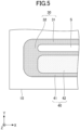
FIG. 3 is a diagram schematically illustrating a state in which a crack is formed in the resistor and the line. As the strain applied to thestrain gauge 1 increases, a crack forms in theresistor 30 and thefirst metal layer 41. According to the study by the inventors, as illustrated inFIG. 3 , a crack C tends to form in the vicinity of the end of thesecond metal layer 42, in the first direction X, that constitutes part of theline 40 so as to extend approximately in the second direction Y. -
FIG. 4 is a partially enlarged plan view of the vicinity of a connection between the resistor and the line inFIG. 1 . As illustrated inFIG. 4 , in thestrain gauge 1, in plan view, the end of thesecond metal layer 42 on one end side (-X side) in the first direction X protrudes further toward the one end side (-X side) in the first direction X than an end of a space S, on the one end side (-X side) in the first direction X, that is situated between thefirst metal layer 41 and theelongated portion 31 that is adjacent to thefirst metal layer 41. That is, when a length by which the end of thesecond metal layer 42 on the one end side in the first direction X protrudes toward the one end side in the first direction X, with reference to the end of the space S on the one end side in the first direction X, is expressed by L1, the length L1 > 0 is satisfied. In thestrain gauge 1, in the plan view, a positional relationship between the end of thesecond metal layer 42 on the one end side in the first direction X, and an end of a space between adjacentelongated portions 31 on one end side in the first direction X may set as desired. -
FIG. 5 is a partially enlarged plan view of the vicinity of the connection between the resistor and the line in the strain gauge in a comparative example. In the comparative example ofFIG. 5 , the length L1 illustrated inFIG. 4 is zero. That is, in the comparative example ofFIG. 5 , in the first direction X, an end of thesecond metal layer 42 on one end side in the first direction X is at the same position as the end of the space S on the one end side in the first direction X. In this case, if the crack C as illustrated inFIG. 3 is formed, theline 40 and theelongated portion 31 adjacent to theline 40 are disconnected and thus the current stops flowing. As a result, the strain gauge in the comparative example ceases to function as a strain gauge. - On the other hand, in the
strain gauge 1 illustrated inFIG. 4 , the length L1 > 0 is satisfied. In this case, even if the crack C as illustrated inFIG. 3 is formed, an electrical connection is maintained without disconnection between theline 40 and theelongated portion 31 adjacent to theline 40, and as a result, the strain gauge can continue to function as the strain gauge. InFIG. 4 , the length L1 is preferably 1 µm or more. In this arrangement, the electrical connection is easily maintained while securing a conduction width between theline 40 and theelongated portion 31 that is adjacent to theline 40. - In
FIG. 4 , the length L1 is more preferably equal to or greater than a length L2 (that is, the width of the elongated portion 31) of theelongated portion 31 in the second direction Y. The length of theelongated portion 31 in the second direction Y is preferably 5 µm or more. That is, the length L1 is more preferably 5 µm or more. As a result, the conduction width between theline 40 and theelongated portion 31 that is adjacent to theline 40 is further secured, and the electrical connection is more easily maintained. - In
FIG. 4 , a length L3 in the first direction X between the end of thefirst metal layer 41 on one end side in the first direction X and the end of thesecond metal layer 42 on one end side in the first direction X is preferably 5 µm or more, and more preferably 10 µm or more. - In a manufacturing process of the
strain gauge 1, afirst metal layer 41 and asecond metal layer 42 are etched and patterned, and thefirst metal layer 41 may be over-etched compared to thesecond metal layer 42, during etching. If the end of thesecond metal layer 42 protrudes in the horizontal direction from the end of thefirst metal layer 41 due to over-etching, the adhesion between theline 40 and thecover layer 60 would decrease when thecover layer 60 covering theline 40 is provided. For example, in theline 40, if thefirst metal layer 41 is formed of a Cr composite film and thesecond metal layer 42 is formed of copper, the Cr composite film is over-etched by about 1 µm to 2 µm in comparison with the copper, during the etching in the manufacturing process of thestrain gauge 1. If the end of thesecond metal layer 42 protrudes in the horizontal direction from the end of thefirst metal layer 41 due to over-etching, in a case where for example, thesecond metal layer 42 is formed of copper, a portion where the copper protrudes oxidizes, and thus the copper degrades. As a result, the reliability of thestrain gauge 1 would decrease. - Therefore, in plan view, the outer edge of the
first metal layer 41 is preferably exposed from thesecond metal layer 42, and the length L3 is preferably 5 µm or more, and more preferably 10 µm or more. In this arrangement, the over-etching of thefirst metal layer 41 relative to thesecond metal layer 42 can be suppressed, and thus the adhesion between theline 40 and thecover layer 60 can be maintained. Even when thesecond metal layer 42 is formed of copper, the copper can be prevented from oxidizing and degrading. -
FIG. 6 is a diagram illustrating an experimental result for strain limits, in which minimum values of the strain limits for a plurality of test strain gauges are plotted. InFIG. 4 , L1 = 0 µm indicates the experimental result for the strain gauge in the comparative example. On the other hand, L1 = 1 µm indicates the experimental result for thestrain gauge 1 according to the first embodiment. - In
FIG. 6 , the vertical axis expresses the strain limit [µST]. The strain limit indicates a value of mechanical strain at which when strain is applied to the strain gauge, the strain gauge becomes unable to function as a strain gauge due to occurrence of a disconnection. From the result ofFIG. 6 , it is confirmed that when L1 = 5 µm, the strain limit is improved by about 1.4 times compared to when L1 = 0 µm. - According to another study by the inventors, it is not preferable that the
second metal layer 42 is not laminated on thefirst metal layer 41. When thesecond metal layer 42 is not laminated on thefirst metal layer 41, the strain limit is further reduced compared to when L1 = 0 µm illustrated inFIG. 6 . For example, when thefirst metal layer 41 is a Cr composite film, in a case where theline 40 is formed of only the Cr composite film, it is considered that the strain limit is reduced because the Cr composite film has poor elasticity. By laminating, on thefirst metal layer 41 made of the Cr composite film, thesecond metal layer 42 made of a material, such as copper, that is superior in elasticity to the Cr composite film, the strain limit can be improved. - That is, from the viewpoint of improving the strain limit, each
line 40 is preferably formed of a laminated structure of thefirst metal layer 41 and thesecond metal layer 42, and thesecond metal layer 42 is preferably formed of a material superior in elasticity to thefirst metal layer 41. That is, the second metal layer is preferably formed of a material that has lower volume resistivity than the first metal layer and that is superior in elasticity to thefirst metal layer 41. In addition to copper, gold, silver, and aluminum are each used as the material that has lower volume resistivity than the first metal layer and that is superior in elasticity to thefirst metal layer 41, when the first metal layer is the Cr composite film. - In the
strain gauge 1 according to the present embodiment, theresistor 30, thelines 40, theelectrodes 50, and thecover layer 60 are formed on thesubstrate 10. Another layer (the functional layer described below, or the like) may be formed between thesubstrate 10 and layers of the above components. - Hereinafter, the method for manufacturing the
strain gauge 1 will be described. In order to manufacture thestrain gauge 1, first, thesubstrate 10 is prepared, and a metal layer (for convenience, a metal layer A is used) is formed on theupper surface 10a of thesubstrate 10. The metal layer A is a layer that is ultimately patterned to serve as theresistor 30, thelines 40, and theelectrodes 50. In this arrangement, the material and thickness of the metal layer A are the same as those of theabove resistor 30 and the like. - The metal layer A can be formed, for example, by magnetron sputtering that uses a raw material capable of forming the metal layer A as a target. Instead of magnetron sputtering, the metal layer A may be formed by reactive sputtering, vapor deposition, arc ion plating, pulsed laser deposition, or the like.
- The metal layer A may be formed after forming a base layer on the
upper surface 10a of thesubstrate 10. For example, a functional layer having a predetermined film thickness may be vacuum-deposited on theupper surface 10a of thesubstrate 10 by conventional sputtering. By providing the base layer in this manner, gauge characteristics of thestrain gauge 1 can be stabilized. - In the present application, the functional layer refers to a layer having a function of promoting crystal growth of at least an upper metal layer A (resistor 30). Preferably, the functional layer further has a function of preventing oxidation of the metal layer A due to oxygen or moisture contained in the
substrate 10 and/or a function of improving adhesion between thesubstrate 10 and the metal layer A. The functional layer may further have other functions. - The insulating resin film that constitutes the
substrate 10 may contain oxygen or moisture, and Cr may form an autoxidized film. In this case, especially when the metal layer A includes Cr, it is preferable to deposit a functional layer having a function of preventing oxidation of the metal layer A. - With this arrangement, by providing the functional layer under the metal layer A, crystal growth of the metal layer A can be promoted, and the metal layer A having a stable crystal phase can be produced. As a result, the stability of the gauge characteristics is improved in the
strain gauge 1. Moreover, the gauge characteristics are improved in thestrain gauge 1 by diffusing a material constituting the functional layer into the metal layer A. - The material of the functional layer may include, for example, one or more metals selected from the group consisting of Cr (chromium), Ti (titanium), V (vanadium), Nb (niobium), Ta (tantalum), Ni (nickel), Y (yttrium), Zr (zirconium), Hf (hafnium), Si (silicon), C (carbon), Zn (zinc), Cu (copper), Bi (bismuth), Fe (iron), Mo (molybdenum), W (tungsten), Ru (ruthenium), Rh (rhodium), Re (rhenium), Os (osmium), Ir (iridium), Pt (platinum), Pd (palladium), Ag (silver), Au (gold), Co (cobalt), Mn (manganese), and Al (aluminum); an alloy of any metals among the group; or a compound of any metal among the group.
-
FIG. 7 is a cross-sectional view (part 2) illustrating the strain gauge according to the first embodiment.FIG. 7 shows a cross-sectional shape of thestrain gauge 1 when afunctional layer 20 is provided as an underlayer of theresistor 30, thelines 40, and theelectrodes 50. - The planar shape of the
functional layer 20 may be patterned to be substantially the same as the planar shape of theresistor 30, thelines 40, and theelectrodes 50, for example. However, the planar shape of thefunctional layer 20 may not be substantially the same as the planar shape of theresistor 30, thelines 40, and theelectrodes 50. For example, when thefunctional layer 20 is formed of an insulating material, thefunctional layer 20 may be patterned to have a shape different from the planar shape of theresistor 30, thelines 40, and theelectrodes 50. In this case, thefunctional layer 20 may be formed in a solid shape in a region where theresistor 30, thelines 40, and theelectrodes 50 are formed, for example. Alternatively, thefunctional layer 20 may be solidly formed on the entire upper surface of thesubstrate 10. - Next, second metal layers 42 and second metal layers 52 are formed on the upper surface of the metal layer A. The second metal layers 42 and the second metal layers 52 can be formed into a predetermined pattern by, for example, known photolithography.
- Next, a photosensitive resist is formed on the upper surface of the metal layer A, the upper surfaces of the second metal layers 42, and the upper surfaces of the second metal layers 52, and the resist is exposed and developed to pattern into a planar shape that is the same as that of the
resistor 30, thelines 40, and theelectrodes 50 illustrated inFIG. 1 . Then, using the resist as an etching mask, the metal layer A exposed from the resist is removed by wet etching or the like. Next, by removing the resist, theresistor 30, thelines 40, and theelectrodes 50 that are in the planar shape illustrated inFIG. 1 can be formed. At this time, the shape of the resist is controlled so that the first metal layers 41 are each not over-etched relative to thesecond metal layer 42. - After the
resistor 30, thelines 40, and theelectrodes 50 are formed, thecover layer 60 is formed on theupper surface 10a of thesubstrate 10 as necessary. Thecover layer 60 covers theresistor 30 and thelines 40, but theelectrodes 50 may be exposed from thecover layer 60. For example, thecover layer 60 can be formed by: laminating a semi-cured thermosetting insulating resin film on theupper surface 10a of thesubstrate 10 so as to cover theresistor 30 and thelines 40 and expose theelectrodes 50; and then heating and curing the insulating resin film. Through the above process, thestrain gauge 1 is completed. - The preferred embodiments and the like are described in detail. However, the strain gauge in the present disclosure is not limited to the above-described embodiments and the like. For example, various modifications and substitutions can be made to the strain gauge according to the above-described embodiments and the like without departing from the scope set forth in the claims.
- This international application claims priority to
Japanese Patent Application No. 2022-076117, filed on May 2, 2022 - 1 strain gauge, 10 substrate, 10a upper surface, 20 functional layer, 30 resistor, 30e1, 30e2 end, 31 elongated portion, 32 folded portion, 40 line, 41, 51 first metal layer, 42, 52 second metal layer, 50 electrode, 60 cover layer
Claims (8)
- A strain gauge comprising:a substrate;a resistor formed on the substrate; andtwo lines formed on the substrate and coupled in series to both ends of the resistor,wherein the resistor includes multiple elongated portions, whose longitudinal directions are aligned with a first direction and which are coupled in series with each other, are arranged side by side,wherein one of the lines is disposed parallel to a given elongated portion, among the multiple elongated portions, that is located at one end in a second direction perpendicular to the first direction,wherein the one line is coupled to one end of the given elongated portion in the first direction,wherein the other of the lines is disposed parallel to a given elongated portion, among the multiple elongated portions, that is located at the other end in the second direction,wherein the other line is coupled to one end of the given elongated portion in the first direction,wherein each of the lines includes a first metal layer and a second metal layer that is laminated on the first metal layer and is formed of a material having lower volume resistivity than the first metal layer,wherein in plan view, an outer edge of the first metal layer is exposed from the second metal layer, wherein in plan view, an end of the second metal layer on one end side in the first direction protrudes further toward the one end side in the first direction than an end of a space that is situated between the first metal layer and the elongated portion adjacent to the first metal layer.
- The strain gauge according to claim 1, wherein a length by which the end of the second metal layer on the one end side in the first direction protrudes toward the one end side in the first direction, with respect to the end of the space on the one end side in the first direction, is 1 µm or more.
- The strain gauge according to claim 2, wherein the length by which the end of the second metal layer protrudes is equal to or greater than a length of each elongated portion of the multiple elongated portions in the second direction.
- The strain gauge according to claim 3, wherein the length of the elongated portion in the second direction is 5 µm or more.
- The strain gauge according to any one of claims 1 to 4, wherein a length in the first direction between an end of the first metal layer on the one end side in the first direction and the end of the second metal layer on the one end side in the first direction is 5 µm or more.
- The strain gauge as claimed in any one of claims 1 to 5, wherein the second metal layer is formed of a material having superior elasticity to the first metal layer.
- The strain gauge according to any one of claims 1 to 6, wherein the first metal layer is integrally formed with the resistor by a same material.
- The strain gauge according to any one of claims 1 to 7, wherein the resistor is formed of a film including Cr, CrN, and Cr2N.
Applications Claiming Priority (2)
| Application Number | Priority Date | Filing Date | Title |
|---|---|---|---|
| JP2022076117A JP7779799B2 (en) | 2022-05-02 | 2022-05-02 | strain gauge |
| PCT/JP2023/016698 WO2023214537A1 (en) | 2022-05-02 | 2023-04-27 | Strain gauge |
Publications (2)
| Publication Number | Publication Date |
|---|---|
| EP4521057A1 true EP4521057A1 (en) | 2025-03-12 |
| EP4521057A4 EP4521057A4 (en) | 2026-04-29 |
Family
ID=88646471
Family Applications (1)
| Application Number | Title | Priority Date | Filing Date |
|---|---|---|---|
| EP23799467.8A Pending EP4521057A4 (en) | 2022-05-02 | 2023-04-27 | EXTENSION METER |
Country Status (5)
| Country | Link |
|---|---|
| US (2) | US12359990B2 (en) |
| EP (1) | EP4521057A4 (en) |
| JP (2) | JP7779799B2 (en) |
| CN (2) | CN120403416A (en) |
| WO (1) | WO2023214537A1 (en) |
Family Cites Families (11)
| Publication number | Priority date | Publication date | Assignee | Title |
|---|---|---|---|---|
| JPH04274703A (en) * | 1991-02-28 | 1992-09-30 | Kyowa Electron Instr Co Ltd | Forming method of electrode of metallic foil strain gauge |
| CN103604363B (en) * | 2013-11-30 | 2017-08-29 | 中航电测仪器股份有限公司 | One kind plastic deformation test strain gauge and its manufacture and scaling method |
| JP6162670B2 (en) | 2014-10-03 | 2017-07-12 | 株式会社東京測器研究所 | Strain gauge alloys and strain gauges |
| JP2019132790A (en) | 2018-02-02 | 2019-08-08 | ミネベアミツミ株式会社 | Strain gauge |
| CN110736421A (en) * | 2019-11-21 | 2020-01-31 | 中国船舶重工集团公司第七0四研究所 | Thin film strain gauge for elastic body strain measurement and preparation method |
| JP7469933B2 (en) * | 2020-03-30 | 2024-04-17 | ミネベアミツミ株式会社 | Strain gauges |
| JP7737790B2 (en) | 2020-10-16 | 2025-09-11 | ミネベアミツミ株式会社 | strain gauge |
| JP2022076117A (en) | 2020-11-09 | 2022-05-19 | 国立大学法人大阪大学 | Method for testing prostate cancer |
| JP7189240B2 (en) * | 2021-01-18 | 2022-12-13 | ミネベアミツミ株式会社 | strain gauge |
| CN214843003U (en) * | 2021-07-13 | 2021-11-23 | 张继华 | Temperature compensation type semiconductor strain gauge |
| CN114045467B (en) * | 2021-11-09 | 2023-12-01 | 北京石墨烯技术研究院有限公司 | Preparation method of flexible strain sensor and flexible strain sensor |
-
2022
- 2022-05-02 JP JP2022076117A patent/JP7779799B2/en active Active
-
2023
- 2023-04-27 CN CN202510602609.4A patent/CN120403416A/en active Pending
- 2023-04-27 EP EP23799467.8A patent/EP4521057A4/en active Pending
- 2023-04-27 CN CN202380037897.2A patent/CN119137441B/en active Active
- 2023-04-27 US US18/861,732 patent/US12359990B2/en active Active
- 2023-04-27 WO PCT/JP2023/016698 patent/WO2023214537A1/en not_active Ceased
-
2025
- 2025-06-18 US US19/242,342 patent/US20250314539A1/en active Pending
- 2025-11-20 JP JP2025200497A patent/JP2026026108A/en active Pending
Also Published As
| Publication number | Publication date |
|---|---|
| US20250172444A1 (en) | 2025-05-29 |
| JP7779799B2 (en) | 2025-12-03 |
| CN120403416A (en) | 2025-08-01 |
| WO2023214537A1 (en) | 2023-11-09 |
| JP2026026108A (en) | 2026-02-16 |
| EP4521057A4 (en) | 2026-04-29 |
| US20250314539A1 (en) | 2025-10-09 |
| CN119137441A (en) | 2024-12-13 |
| US12359990B2 (en) | 2025-07-15 |
| JP2023165275A (en) | 2023-11-15 |
| CN119137441B (en) | 2025-05-30 |
Similar Documents
| Publication | Publication Date | Title |
|---|---|---|
| US11499877B2 (en) | Strain gauge | |
| JP2022189613A (en) | strain gauge | |
| US12379268B2 (en) | Strain gauge | |
| EP4261494A1 (en) | Strain gauge | |
| US12523461B2 (en) | Strain gauge | |
| JP2025170444A (en) | Strain Detection System | |
| WO2022080421A1 (en) | Strain gauge | |
| EP4567370A1 (en) | Strain gauge | |
| US12359990B2 (en) | Strain gauge | |
| JP7697758B2 (en) | Strain gauges | |
| JP2022008026A (en) | Strain gauge | |
| EP4567369A1 (en) | Strain gauge | |
| EP4675221A1 (en) | Strain gauge and strain sensor | |
| EP4553446A1 (en) | Strain gauge | |
| US12595998B2 (en) | Strain gauge | |
| JP2023136681A (en) | strain gauge | |
| JP2023136406A (en) | strain gauge | |
| JP2023138128A (en) | strain gauge |
Legal Events
| Date | Code | Title | Description |
|---|---|---|---|
| STAA | Information on the status of an ep patent application or granted ep patent |
Free format text: STATUS: THE INTERNATIONAL PUBLICATION HAS BEEN MADE |
|
| PUAI | Public reference made under article 153(3) epc to a published international application that has entered the european phase |
Free format text: ORIGINAL CODE: 0009012 |
|
| STAA | Information on the status of an ep patent application or granted ep patent |
Free format text: STATUS: REQUEST FOR EXAMINATION WAS MADE |
|
| 17P | Request for examination filed |
Effective date: 20241031 |
|
| AK | Designated contracting states |
Kind code of ref document: A1 Designated state(s): AL AT BE BG CH CY CZ DE DK EE ES FI FR GB GR HR HU IE IS IT LI LT LU LV MC ME MK MT NL NO PL PT RO RS SE SI SK SM TR |
|
| DAV | Request for validation of the european patent (deleted) | ||
| DAX | Request for extension of the european patent (deleted) | ||
| P01 | Opt-out of the competence of the unified patent court (upc) registered |
Free format text: CASE NUMBER: UPC_APP_0003839_4521057/2026 Effective date: 20260203 |
|
| A4 | Supplementary search report drawn up and despatched |
Effective date: 20260401 |
|
| RIC1 | Information provided on ipc code assigned before grant |
Ipc: G01B 7/16 20060101AFI20260326BHEP Ipc: G01L 1/22 20060101ALI20260326BHEP |