EP4518632A1 - Display device - Google Patents
Display device Download PDFInfo
- Publication number
- EP4518632A1 EP4518632A1 EP24189114.2A EP24189114A EP4518632A1 EP 4518632 A1 EP4518632 A1 EP 4518632A1 EP 24189114 A EP24189114 A EP 24189114A EP 4518632 A1 EP4518632 A1 EP 4518632A1
- Authority
- EP
- European Patent Office
- Prior art keywords
- dam
- layer
- disposed
- display area
- touch
- Prior art date
- Legal status (The legal status is an assumption and is not a legal conclusion. Google has not performed a legal analysis and makes no representation as to the accuracy of the status listed.)
- Pending
Links
Images



Classifications
-
- G—PHYSICS
- G06—COMPUTING OR CALCULATING; COUNTING
- G06F—ELECTRIC DIGITAL DATA PROCESSING
- G06F3/00—Input arrangements for transferring data to be processed into a form capable of being handled by the computer; Output arrangements for transferring data from processing unit to output unit, e.g. interface arrangements
- G06F3/01—Input arrangements or combined input and output arrangements for interaction between user and computer
- G06F3/03—Arrangements for converting the position or the displacement of a member into a coded form
- G06F3/041—Digitisers, e.g. for touch screens or touch pads, characterised by the transducing means
-
- G—PHYSICS
- G06—COMPUTING OR CALCULATING; COUNTING
- G06F—ELECTRIC DIGITAL DATA PROCESSING
- G06F3/00—Input arrangements for transferring data to be processed into a form capable of being handled by the computer; Output arrangements for transferring data from processing unit to output unit, e.g. interface arrangements
- G06F3/01—Input arrangements or combined input and output arrangements for interaction between user and computer
- G06F3/03—Arrangements for converting the position or the displacement of a member into a coded form
- G06F3/041—Digitisers, e.g. for touch screens or touch pads, characterised by the transducing means
- G06F3/0412—Digitisers structurally integrated in a display
-
- G—PHYSICS
- G06—COMPUTING OR CALCULATING; COUNTING
- G06F—ELECTRIC DIGITAL DATA PROCESSING
- G06F3/00—Input arrangements for transferring data to be processed into a form capable of being handled by the computer; Output arrangements for transferring data from processing unit to output unit, e.g. interface arrangements
- G06F3/01—Input arrangements or combined input and output arrangements for interaction between user and computer
- G06F3/03—Arrangements for converting the position or the displacement of a member into a coded form
- G06F3/041—Digitisers, e.g. for touch screens or touch pads, characterised by the transducing means
- G06F3/0416—Control or interface arrangements specially adapted for digitisers
-
- G—PHYSICS
- G06—COMPUTING OR CALCULATING; COUNTING
- G06F—ELECTRIC DIGITAL DATA PROCESSING
- G06F3/00—Input arrangements for transferring data to be processed into a form capable of being handled by the computer; Output arrangements for transferring data from processing unit to output unit, e.g. interface arrangements
- G06F3/01—Input arrangements or combined input and output arrangements for interaction between user and computer
- G06F3/03—Arrangements for converting the position or the displacement of a member into a coded form
- G06F3/041—Digitisers, e.g. for touch screens or touch pads, characterised by the transducing means
- G06F3/044—Digitisers, e.g. for touch screens or touch pads, characterised by the transducing means by capacitive means
-
- G—PHYSICS
- G06—COMPUTING OR CALCULATING; COUNTING
- G06F—ELECTRIC DIGITAL DATA PROCESSING
- G06F3/00—Input arrangements for transferring data to be processed into a form capable of being handled by the computer; Output arrangements for transferring data from processing unit to output unit, e.g. interface arrangements
- G06F3/01—Input arrangements or combined input and output arrangements for interaction between user and computer
- G06F3/03—Arrangements for converting the position or the displacement of a member into a coded form
- G06F3/041—Digitisers, e.g. for touch screens or touch pads, characterised by the transducing means
- G06F3/044—Digitisers, e.g. for touch screens or touch pads, characterised by the transducing means by capacitive means
- G06F3/0445—Digitisers, e.g. for touch screens or touch pads, characterised by the transducing means by capacitive means using two or more layers of sensing electrodes, e.g. using two layers of electrodes separated by a dielectric layer
-
- G—PHYSICS
- G06—COMPUTING OR CALCULATING; COUNTING
- G06F—ELECTRIC DIGITAL DATA PROCESSING
- G06F3/00—Input arrangements for transferring data to be processed into a form capable of being handled by the computer; Output arrangements for transferring data from processing unit to output unit, e.g. interface arrangements
- G06F3/01—Input arrangements or combined input and output arrangements for interaction between user and computer
- G06F3/03—Arrangements for converting the position or the displacement of a member into a coded form
- G06F3/041—Digitisers, e.g. for touch screens or touch pads, characterised by the transducing means
- G06F3/044—Digitisers, e.g. for touch screens or touch pads, characterised by the transducing means by capacitive means
- G06F3/0446—Digitisers, e.g. for touch screens or touch pads, characterised by the transducing means by capacitive means using a grid-like structure of electrodes in at least two directions, e.g. using row and column electrodes
-
- H—ELECTRICITY
- H10—SEMICONDUCTOR DEVICES; ELECTRIC SOLID-STATE DEVICES NOT OTHERWISE PROVIDED FOR
- H10K—ORGANIC ELECTRIC SOLID-STATE DEVICES
- H10K59/00—Integrated devices, or assemblies of multiple devices, comprising at least one organic light-emitting element covered by group H10K50/00
- H10K59/10—OLED displays
- H10K59/12—Active-matrix OLED [AMOLED] displays
- H10K59/1201—Manufacture or treatment
-
- H—ELECTRICITY
- H10—SEMICONDUCTOR DEVICES; ELECTRIC SOLID-STATE DEVICES NOT OTHERWISE PROVIDED FOR
- H10K—ORGANIC ELECTRIC SOLID-STATE DEVICES
- H10K59/00—Integrated devices, or assemblies of multiple devices, comprising at least one organic light-emitting element covered by group H10K50/00
- H10K59/10—OLED displays
- H10K59/12—Active-matrix OLED [AMOLED] displays
- H10K59/122—Pixel-defining structures or layers, e.g. banks
-
- H—ELECTRICITY
- H10—SEMICONDUCTOR DEVICES; ELECTRIC SOLID-STATE DEVICES NOT OTHERWISE PROVIDED FOR
- H10K—ORGANIC ELECTRIC SOLID-STATE DEVICES
- H10K59/00—Integrated devices, or assemblies of multiple devices, comprising at least one organic light-emitting element covered by group H10K50/00
- H10K59/40—OLEDs integrated with touch screens
-
- H—ELECTRICITY
- H10—SEMICONDUCTOR DEVICES; ELECTRIC SOLID-STATE DEVICES NOT OTHERWISE PROVIDED FOR
- H10K—ORGANIC ELECTRIC SOLID-STATE DEVICES
- H10K59/00—Integrated devices, or assemblies of multiple devices, comprising at least one organic light-emitting element covered by group H10K50/00
- H10K59/80—Constructional details
- H10K59/87—Passivation; Containers; Encapsulations
- H10K59/873—Encapsulations
-
- G—PHYSICS
- G06—COMPUTING OR CALCULATING; COUNTING
- G06F—ELECTRIC DIGITAL DATA PROCESSING
- G06F2203/00—Indexing scheme relating to G06F3/00 - G06F3/048
- G06F2203/041—Indexing scheme relating to G06F3/041 - G06F3/045
- G06F2203/04102—Flexible digitiser, i.e. constructional details for allowing the whole digitising part of a device to be flexed or rolled like a sheet of paper
-
- G—PHYSICS
- G06—COMPUTING OR CALCULATING; COUNTING
- G06F—ELECTRIC DIGITAL DATA PROCESSING
- G06F2203/00—Indexing scheme relating to G06F3/00 - G06F3/048
- G06F2203/041—Indexing scheme relating to G06F3/041 - G06F3/045
- G06F2203/04103—Manufacturing, i.e. details related to manufacturing processes specially suited for touch sensitive devices
-
- G—PHYSICS
- G06—COMPUTING OR CALCULATING; COUNTING
- G06F—ELECTRIC DIGITAL DATA PROCESSING
- G06F2203/00—Indexing scheme relating to G06F3/00 - G06F3/048
- G06F2203/041—Indexing scheme relating to G06F3/041 - G06F3/045
- G06F2203/04111—Cross over in capacitive digitiser, i.e. details of structures for connecting electrodes of the sensing pattern where the connections cross each other, e.g. bridge structures comprising an insulating layer, or vias through substrate
-
- H—ELECTRICITY
- H10—SEMICONDUCTOR DEVICES; ELECTRIC SOLID-STATE DEVICES NOT OTHERWISE PROVIDED FOR
- H10K—ORGANIC ELECTRIC SOLID-STATE DEVICES
- H10K2102/00—Constructional details relating to the organic devices covered by this subclass
- H10K2102/301—Details of OLEDs
- H10K2102/311—Flexible OLED
Definitions
- the present disclosure relates to a display device and a method of manufacturing the same.
- LCD liquid crystal display
- OLED organic light emitting diode
- a display device may include a display panel and a touch sensor layer, and the touch sensor layer may be attached to the display panel as a separate layer from the display panel, but may also be disposed directly on the display panel.
- the present disclosure is directed to providing a display device manufactured using a fewer number of masks.
- a display device includes a base substrate including a display area including a plurality of pixels, and a non-display area near the display area, a first dam disposed on the base substrate of the non-display area, a second dam disposed on the base substrate of the non-display area and disposed between the first dam and the display area, and a touch sensor layer including a touch conductive layer disposed between the first dam and the second dam and a touch organic layer on the touch conductive layer, wherein the touch organic layer ends inside the first dam, and the first dam and the second dam include the same material.
- a display device includes a display area including a plurality of pixels, and a non-display area located near the display area, wherein the non-display area includes a first dam part surrounding the display area, and a second dam part surrounding the display area and disposed between the first dam part and the display area, and the first dam part includes a main dam portion having a first separation distance to the second dam part, and a protruding dam portion having a second separation distance to the second dam part.
- a display device comprises: a base substrate including a display area including a plurality of pixels, and a non-display area near or adjacent to the display area; a first dam disposed on the base substrate of the non-display area; a second dam disposed on the base substrate of the non-display area and disposed between the first dam and the display area.
- the display device may comprise a touch sensor layer including: a touch conductive layer disposed between the first dam and the second dam, and a touch organic layer on the touch conductive layer.
- the touch organic layer may end inside the first dam.
- the touch organic layer may have an end disposed on or inside or within the first dam.
- the first dam may surround the touch organic layer, in particular an end of the touch organic layer.
- the first dam and the second dam may include the same material.
- a display device comprises: a display area including a plurality of pixels; and a non-display area located near the display area.
- the non-display area may include: a first dam part surrounding the display area; and a second dam part surrounding the display area and disposed between the first dam part and the display area.
- the first dam part may include: a main dam portion having a first separation distance to the second dam part; and a protruding dam portion having a second separation distance to the second dam part.
- a display device may include one or several of the following optional features.
- a height of the first dam may be greater than a surface height of the second dam.
- a height of an upper surface of the first dam may be greater than a surface height of an upper surface of the second dam, as measured from the base substrate.
- the display device may further comprise a thin film encapsulation layer between the first dam and the touch sensor layer.
- the thin film encapsulation layer may include a first encapsulation inorganic layer, and/or an encapsulation organic layer disposed on the first encapsulation inorganic layer, and/or a second encapsulation inorganic layer disposed on the encapsulation organic layer.
- the encapsulation organic layer may end inside the second dam.
- the encapsulation organic layer may have an end disposed on or inside or within the second dam.
- the second dam may surround the encapsulation organic layer, in particular an end of the encapsulation organic layer.
- the encapsulation organic layer may not overlap the first dam, in particular in a thickness direction of the display device.
- the non-display area may include a bending region in which the display device is bent in a thickness direction.
- the first dam may be disposed in the bending region.
- the second dam may be disposed between the bending region and the display area.
- the display device may further comprise an organic element layer disposed on the base substrate of the display area.
- the organic element layer may include an anode, a bank layer exposing a portion of an upper surface of the anode, an organic layer disposed on the exposed upper surface of the anode, and a cathode disposed on the organic layer.
- the first dam and the second dam may be disposed coplanar with the bank layer.
- An upper surface of the first is coplanar with an upper surface of the bank layer.
- An upper surface of the second dam is coplanar with a lower surface of the bank layer.
- the two or more first dams may be provided.
- the first dam may be disposed on a second interlayer insulating layer between the bank layer and the base substrate.
- the second interlayer insulating layer may be disposed on the base substrate in the non-display area.
- the second layer insulating layer may be further disposed in the display area between the bank layer and the base substrate.
- the first dam may be disposed on a planarization layer between the bank layer and the base substrate.
- the planarization layer may be disposed on the base substrate in the non-display area.
- the planarization layer may be further disposed in the display area between the bank layer and the base substrate.
- the planarization layer may be disposed between the second interlayer insulating layer and the bank layer.
- the first dam may be disposed on the second interlayer insulating layer and the planarization layer.
- the first dam part may further include a connection dam portion connecting the main dam portion with the protruding dam portion.
- the non-display area may further include a bending region in which the display device is bent in a thickness direction.
- the protruding dam portion may be disposed in the bending region.
- the second separation distance may be greater than the first separation distance.
- the first dam part may include the first dam.
- the second dam part may include the second dam.
- the embodiments by omitting one of the plurality of touch organic layers of the conventional touch sensor layer, it is possible to reduce the number of masks and simplify the manufacturing of the display device.
- the one touch organic layer includes a dam for preventing the overflow of the other organic layer to the pad part.
- the dam since the one touch organic layer is omitted, the dam may be formed using at least one of the organic layers of the display panel. In other words, by forming the dam for simplifying the stacking structure of the display device and preventing the overflow of the other organic layer to the pad part using the at least one of the organic layers of the display panel, it is possible to prevent the overflow of the other touch organic layer to the pad part.
- first component or an area, a layer, a portion, or the like
- first component or an area, a layer, a portion, or the like
- first component may be directly connected/coupled to the second component or a third component may be disposed therebetween.
- first and second may be used to describe various components, but the components are not limited by the terms. The terms are used only for the purpose of distinguishing one component from another. For example, a first component may be referred to as a second component, and similarly, the second component may also be referred to as the first component without departing from the scopes of the embodiments.
- the singular expression includes the plural expression unless the context clearly dictates otherwise.
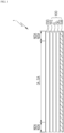
- FIG. 1 is a schematic cross-sectional view of a display device according to one embodiment.
- a display device 1 may include a display panel 100, and a touch sensor layer 200 formed on the display panel 100.
- the display panel 100 may include a substrate part SUB, a circuit element layer CEL formed on the substrate part SUB, an organic element layer EL formed on the circuit element layer CEL, a thin film encapsulation layer TFE formed on the organic element layer EL, and the touch sensor layer 200 formed on the thin film encapsulation layer TFE.
- the display panel 100 may be an organic light emitting display panel including the organic element layer EL.
- the display panel 100 is not limited thereto and may be a liquid crystal display panel or an inorganic light emitting display panel.
- an example in which the display panel 100 is the organic light emitting display panel will be mainly described.
- the display device 1 may include a display area DA and a non-display area NDA near the display area DA.
- the display area DA may include a plurality of pixels to generate or display images.
- the non-display area NDA may not generate the images.
- the non-display area NDA may not include pixels, but is not limited thereto.
- the non-display area NDA may surround the display area DA.
- the non-display area may be arranged at a periphery of the display area DA.
- the display device 1 may further include a sensing area SA and a non-sensing area NSA near the sensing area SA.
- the sensing area SA and the non-sensing area NSA may correspond to the display area DA and the non-display area NDA, respectively, and may have the same area, but are not limited thereto.
- the sensing area SA may be an area in which touch electrodes TE and RE to be described below in FIG. 4 are disposed, and a touch line TL connected to the touch electrodes TE and RE, touch pads TPAD connected to the touch line TL, etc. may be disposed in the non-sensing area NSA.
- the substrate part SUB, the circuit element layer CEL, the organic element layer EL, the thin film encapsulation layer TFE, and the touch sensor layer 200 will be described below.
- FIG. 2 is a plan view of the display device according to FIG. 1 .
- a planar shape of the display area DA may have a rectangular shape.
- the present disclosure is not limited thereto, and the planar shape of the display area DA may be a square, circular, elliptical, or other polygonal shapes.
- the display area DA may have a rectangular shape with rounded corners, but is not limited thereto and may also have a rectangular shape with angled corners.
- a first direction DR1 also referred to as a horizontal direction
- a second direction DR2 also referred to as a vertical direction
- a third direction DR3 is a direction that intersects the plane on which the first direction DR1 and the second direction DR2 are present when the display device is not bent, for example, a direction perpendicular to both the first direction DR1 and the second direction DR2.
- the first direction DR1 may be the same as extending directions of short sides of the display panel 100
- the second direction DR2 may the same as extending directions of long sides of the display panel 100
- the third direction DR3 may be the same as a stacking direction of the substrate part SUB, the circuit element layer CEL, the organic element layer EL, thin film encapsulation layer TFE, and the touch sensor layer 200 in FIG. 1 .
- the directions described in the embodiment should be understood as indicating relative directions, and the embodiment is not limited to the described direction.
- the display area DA may include short sides extending in the first direction DR1 and long sides extending in the second direction DR2.
- the non-display area NDA may surround the display area DA.
- the non-display area NDA may be disposed at one , i.e. left, side and the other, i.e. right, side of the display area DA in the first direction DR1 and one, i.e. upper, side and the other, i.e. lower, side of the display area DA in the second direction DR2. Portions of the non-display area NDA may substantially form a ring.
- the non-display area NDA or portions thereof may surround the display area DA.
- the non-display area NDA or at least portions thereof may be arranged to be adjacent to the display area DA.
- the non-display area NDA located at the other side of the display area DA in the second direction DR2 may extend further from a central portion of the one side of the display area DA in the second direction DR2 toward the other side in the second direction DR2.
- a width of the non-display area NDA in the first direction DR1 further extending from the central portion of the other side of the display area DA in the second direction DR2 toward the other side in the second direction DR2 may be smaller than a width of the non-display area NDA in the first direction DR1 adjacent to the other side of the display area DA in the second direction DR2.
- the portion of the non-display area NDA arranged at the lower side of the display area DA may be wider than the portion of the non-display area NDA arranged at the upper side of the display area DA.
- the display device 1 may include a main region MR, a sub-region SR, and a bending region BR between the main region MR and the sub-region SR.
- the display area DA and the portions of the non-display area NDA surrounding the display area DA on all four surfaces or sides of the display area DA form the main region MR.
- a portion extending from the central portion of the other side of the display area DA in the second direction DR2 toward the other side in the second direction DR2 may form the bending region BR and the sub-region SR.
- a portion of the non-display area NDA extending from the portion of the non-display area NDA arranged at the lower side of the non-display area may form the bending region BR and the sub-region SR.
- the main region MR may be arranged between the display area DA and the bending region BR.
- the main region MR, the bending region BR and the sub-region SR may be arranged at the lower side of the display area DA and/or may be arranged in this order starting from the display area DA against the second direction DR2.
- the bending region BR may be disposed between the sub-region SR and the main region MR.
- the sub-region SR may include a first pad area PA1 and a second pad area PA2.
- the second pad area PA2 may be located at an end portion of the other side of the sub-region SR in the second direction DR2.
- the first pad area PA1 may be arranged to be adjacent to the bending region BR.
- the second pad area PA2 may be arranged to be adjacent to the first pad area PA1 and/or may extend away from the first pad area PA1 against the second direction DR2.
- the first pad area PA1 may be arranged between the bending region BR and the second pad area PA2.
- the display device 1 may further include a data driver 300 and a printed circuit board 500.
- the data driver 300 may be disposed in the first pad area PA1, and the printed circuit board 500 may be attached to the second pad area PA2.
- a plurality of pads connected to the data driver 300 and the printed circuit board 500 may be disposed in each of the first pad area PA1 and the second pad area PA2.
- the data driver 300 may be formed, for example, in the form of a driving chip (IC), but is not limited thereto.
- IC driving chip
- an example in which the data driver 300 is disposed in a chip on plastic type that is directly mounted on the display panel 100 is described, but the present disclosure is not limited thereto and is disposed in a chip on glass type or a chip on film type.
- the display area DA may include a plurality of pixels PX.
- the plurality of pixels PX may each be connected to a scan line SL and a data line DL.
- the pixel PX may include and/or may be connected to a high voltage power line, a low voltage power line, or various lines in the art.
- the pixel PX may include a capacitor.
- the display device 1 may further include a first dam part DP1 and a second dam part DP2.
- the first dam part DP1 and the second dam part DP2 may each surround the display area DA.
- the first dam part DP1 and the second dam part DP2 may each have a closed loop shape that fully surrounds the display area DA.
- the second dam part DP2 may be disposed between the first dam part DP1 and the display area DA.
- the second dam part DP2 may be disposed between the display area DA and the bending region BR to be described below.
- the first dam part DP1 and the second dam part DP2 may each be disposed in the non-display area NDA.
- the second dam part DP2 may be disposed in the non-display area NDA adjacent to the display area DA and disposed in the main region MR.
- the first dam part DP1 may be disposed outside the second dam part DP2, i.e. may surround the second dam part DP2.
- the first dam part DP1 may include a main dam portion DP1a, a protruding dam portion DP1b, and a connection dam portion DP1c.
- the main dam portion DP1a may be disposed at one side and the other side of the display area DA in the first direction DR1 and disposed in the non-display area NDA disposed adjacent to the one side of the display area DA in the second direction DR2.
- the main dam portion DP1a may be disposed at the periphery of the non-display area NDA adjacent to the other side of the display area DA in the second direction DR2.
- the main dam portion DP1a may be disposed in the non-display area NDA arranged at the one side and the other side of the display area DA in the first direction DR1.
- the main dam portion DP1a may be disposed in the non-display area NDA arranged at the one side of the display area DA in the second direction DR2.
- the main dam portion DP1a may be disposed in the non-display area NDA arranged at the other side of the display area DA in the second direction DR2.
- the main dam portion DP1a disposed in the non-display area NDA disposed adjacent to the one side and the other side of the display area DA in the first direction DR1 and the one side of the display area DA in the second direction DR2, and at the periphery of the non-display area NDA adjacent to the other side of the display area DA in the second direction DR2 may be formed integrally.
- the main dam portion DP1a may be disposed in the main region MR.
- the protruding dam portion DP1b may be disposed in the bending region BR and may not be disposed in the main region MR.
- the protruding dam portion DP1b may extend along the first direction DR1.
- the main dam portion DP1a disposed in the non-display area NDA arranged at the other side of the display area DA in the second direction DR2 may extend along the first direction DR1.
- the first dam part DP1 and the second dam part DP2 may be arranged to be spaced apart or separated from each other.
- the main dam portion DP1a and the second dam part DP2 may be disposed to have a first separation distance d1
- the protruding dam portion DP1b and the second dam part DP2 may be disposed to have a second separation distance d2 greater than the first separation distance d1.
- the main dam portion DP1a and the protruding dam portion DP1b may be connected through the connection dam portion DP1c.
- the connection dam portion DP1c may extend from the main region MR to the bending region BR.
- connection dam portion DP1c may be disposed throughout the bending region BR and the main region MR, but is not limited thereto. In other words, when the protruding dam portion DP1b is disposed in the bending region BR adjacent to the boundary between the bending region BR and the main region MR, the connection dam portion DP1c may be disposed only in the main region MR.
- the protruding dam portion DP1b may be disposed in the main region MR.
- the second separation distance d2 may be equal to the first separation distance d1.
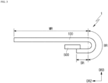
- FIG. 3 is a cross-sectional view showing a bent state of the display device according to FIG. 1 .
- the bending region BR of the display panel 100 of the display device 1 may be bent in the thickness direction (or the third direction DR3). Therefore, the main region MR and the sub-region SR may overlap each other in the thickness direction.
- the display panel 100 may be bent in such a way that a lower surface of the main region MR and an upper surface of the sub-region SR face each other.
- the printed circuit board 500 may be attached to an end portion of the sub-region SR.
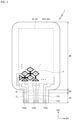
- FIG. 4 is a more detailed plan view of the display device according to FIG. 2 .
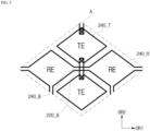
- FIG. 5 is an enlarged plan view of area A of FIG. 4.
- FIG. 4 is a plan view of the display device 1 according to FIG. 2 and specifically shows the touch sensor layer 200 (see FIG. 1 ), and the touch line TL and the touch pad TPAD that are connected to the touch sensor layer 200.
- the touch sensor layer 200 may include a plurality of touch electrodes TE and RE for detecting the user's touch using a capacitance method, and the touch lines TL connecting the plurality of touch electrodes TE and RE with the touch pads TPAD.
- the touch sensor layer 200 may sense the user's touch using a self-capacitance method or a mutual capacitance method.
- a plurality of touch electrodes TE and RE may be disposed in the sensing area SA.
- the plurality of touch electrodes TE and RE may generate a mutual capacitance or a self-capacitance to detect the touch of an object or a person.
- the plurality of touch electrodes TE and RE may include a plurality of driving electrodes TE 240_T and a plurality of detecting electrodes RE 240_R.
- the plurality of driving electrodes TE 240_T may be arranged in the first direction DR1 and the second direction DR2.
- the plurality of driving electrodes TE 240_T may be spaced apart from each other in the first direction DR1 and the second direction DR2.
- the driving electrodes TE 240_T adjacent to each other in the second direction DR2 may be electrically connected through and/or to a bridge electrode 220_B.
- the plurality of detecting electrodes RE 240_R may extend in the first direction DR1 and may be spaced apart from each other in the second direction DR2.
- the plurality of detecting electrodes RE 240_R may be arranged in the first direction DR1 and the second direction DR2.
- the detecting electrodes RE 240_R adjacent to each other in the first direction DR1 may be electrically connected through and/or to a connection part 240_B.
- the plurality of driving electrodes TE 240_T and detecting electrodes RE 240_R may each be connected to a plurality of touch pads TPAD through the touch lines TL.
- the bridge electrode 220_B may be disposed on a different layer from the plurality of driving electrodes TE 240_T and the plurality of detecting electrodes RE 240_R.
- the detecting electrodes RE 240_R adjacent to each other in the first direction DR1 may be electrically connected through the connection part 240_B formed on the same layer as the plurality of driving electrodes TE 240_T or the plurality of detecting electrodes RE 240_R, and the driving electrodes TE 240_T adjacent to each other in the second direction DR2 may be electrically connected through the bridge electrode 220_B formed on a different layer from the plurality of driving electrodes TE 240_T or the plurality of detecting electrodes RE 240_R.
- the bridge electrode 220_B overlaps the plurality of detecting electrodes RE 240_R in the thickness direction DR3, the plurality of driving electrodes TE 240_T and the plurality of detecting electrodes RE 240_R may be insulated from each other.
- the mutual capacitance may be generated between the driving electrode TE 240_T and the detecting electrode RE 240_R.
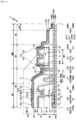
- FIG. 6 is a cross-sectional view along line I-I' in FIG. 2 .
- the display device 1 may include the substrate part SUB, the circuit element layer CEL formed on the substrate part SUB, the organic element layer EL formed on the circuit element layer CEL, the thin film encapsulation layer TFE formed on the organic element layer EL, and the touch sensor layer 200 formed on the thin film encapsulation layer TFE.
- the substrate part SUB may include a base substrate 101.
- the base substrate 101 may support layers disposed thereon.
- the base substrate 101 may be disposed throughout the display area DA and the non-display area NDA.
- the base substrate 101 may be made of an insulating material such as a polymer resin.
- the polymer material may include polyethersulphone (PES), polyacrylate (PA), polyarylate (PAR), polyetherimide (PEI), polyethylene napthalate (PEN), polyethylene terepthalate (PET), polyphenylene sulfide (PPS), polyallylate, polyimide (PI), polycarbonate (PC), cellulose triacetate (CAT), cellulose acetate propionate (CAP), or combinations thereof.
- the base substrate 101 may be a flexible substrate capable of bending, folding, rolling, etc.
- An example of a material forming the flexible substrate may be polyimide (PI), but is not limited thereto.
- the base substrate 101 may be a rigid substrate made of glass, quartz, etc.
- the circuit element layer CEL may be formed on the substrate part SUB.
- the circuit element layer CEL may include a semiconductor layer 105, a gate insulating layer 111 formed on the semiconductor layer 105, a gate conductive layer including a gate electrode GE on the gate insulating layer 111, a first interlayer insulating layer 112 formed on the gate conductive layer, a first source drain conductive layer 130 including a source electrode 131, a drain electrode 133, and a first touch pad portion TPAD1 of a touch pad TPAD, a second interlayer insulating layer 141 formed on the first source drain conductive layer 130, a second source drain conductive layer 150 including a connection electrode 151 formed on the second interlayer insulating layer 141, a second touch pad portion TPAD2 of the touch pad TPAD, and a bending bridge electrode CL, and a first organic layer 160 including a planarization layer 161 formed on the second source drain conductive layer 150 and a second lower dam DAM21.
- the organic element layer EL may include an organic light emitting diode OLED including an anode ANO formed on the first organic layer 160, an organic layer OL, and a cathode electrode CAT, and a second organic layer 170 including a bank layer 171, a second upper dam DAM22, and a first dam DAM1.
- the thin film encapsulation layer TFE may include a first encapsulation inorganic layer 181 formed on the organic element layer EL, an encapsulation organic layer 182 formed on the first encapsulation inorganic layer 181, and a second encapsulation inorganic layer 183 formed on the encapsulation organic layer 182.
- the touch sensor layer 200 may include a touch buffer layer 210 formed on the thin film encapsulation layer TFE, a first touch conductive layer 220 including the bridge electrode 220_B formed on the touch buffer layer 210 and a first touch line portion TL1 of the touch line TL, a touch insulting layer 230 formed on the first touch conductive layer 220, a second touch conductive layer 240 including a driving electrode 240_T formed on the touch insulating layer 230, a second touch line portion TL2 of the touch line TL, and a third touch pad portion TPAD3 of the touch pad TPAD, and a touch organic layer 250 formed on the second touch conductive layer 240.
- a buffer layer may be disposed on the base substrate 101.
- the buffer layer can prevent the diffusion of impurity ions and prevent the permeation of moisture or outside air.
- the buffer layer may include a plurality of layers.
- the buffer layer may be provided as layers formed by alternately stacking silicon nitride (SiNx) and silicon oxide (SiOx) at least once.
- the semiconductor layer 105 may be disposed in the display area DA on the buffer layer.
- the semiconductor layer 105 may include polycrystalline silicon.
- the semiconductor layer 105 may include a channel area, a source area, and a drain area.
- the polycrystalline silicon may be formed by crystallizing amorphous silicon. Examples of the crystallization methods may include a rapid thermal annealing (RTA) method, a solid phase crystallization (SPC) method, an excimer laser annealing (ELA) method, a metal induced crystallization (MIC) method, a metal induced lateral crystallization (MILC) method, a sequential crystallization (SLS) method, etc., but are not limited thereto.
- RTA rapid thermal annealing
- SPC solid phase crystallization
- EVA excimer laser annealing
- MIC metal induced crystallization
- MILC metal induced lateral crystallization
- SLS sequential crystallization
- the gate insulating layer 111 may be formed on the semiconductor layer 105.
- the gate insulating layer 111 may be generally disposed throughout the display area DA and the non-display area NDA.
- the gate insulating layer 111 may be a gate insulating film having a gate insulating function.
- the gate insulating layer 111 may include a silicon compound, metal oxide, etc.
- the gate insulating layer 111 may include silicon oxide, silicon nitride, silicon oxynitride, aluminum oxide, tantalum oxide, hafnium oxide, zirconium oxide, titanium oxide, etc.
- the materials may be used alone or in combination.
- the drawing shows that the gate insulating layer 111 is formed of a single film, in some cases, the gate insulating layer 111 may be a multilayered film formed of stacked films made of different materials.
- the gate conductive layer may be disposed on the gate insulating layer 111.
- the gate conductive layer may include the gate electrode GE.
- the gate conductive layer may further include a scan signal line that transmits a scan signal to the gate electrode GE.
- the gate electrode GE may be disposed to overlap the channel area of the semiconductor layer 105.
- the gate conductive layer may include one or more selected from molybdenum (Mo), aluminum (Al), platinum (Pt), palladium (Pd), silver (Ag), magnesium (Mg), gold (Au), nickel (Ni), neodymium (Nd), iridium (Ir), chromium (Cr), calcium (Ca), titanium (Ti), tantalum (Ta), tungsten (W), and copper (Cu).
- Mo molybdenum
- Al aluminum
- platinum (Pt) palladium
- silver Ag
- magnesium Mg
- gold Au
- nickel (Ni) nickel
- iridium (Ir) chromium
- Cr calcium (Ca), titanium (Ti), tantalum (Ta), tungsten (W), and copper (Cu).
- the gate conductive layer may be formed as a multilayered layer.
- the multilayered film of the gate conductive layer may be formed as a stacked film made of different metal
- the first interlayer insulating layer 112 may be disposed on the gate conductive layer.
- the first interlayer insulating layer 112 may be disposed throughout the display area DA and the non-display area NDA.
- the first interlayer insulating layer 112 may insulate the gate conductive layer and the first source drain conductive layer 130.
- the first interlayer insulating layer 112 may be an interlayer insulating film.
- the first interlayer insulating layer 112 may include an inorganic insulating material such as silicon oxide, silicon nitride, silicon oxynitride, hafnium oxide, aluminum oxide, titanium oxide, tantalum oxide, or zinc oxide, or an organic insulating material such as a polyacrylates resin, an epoxy resin, a phenolic resin, a polyamides resin, a polyimides rein, an unsaturated polyesters resin, a polyphenylenethers resin, a polyphenylenesulfides resin or benzocyclobutene (BCB).
- an inorganic insulating material such as silicon oxide, silicon nitride, silicon oxynitride, hafnium oxide, aluminum oxide, titanium oxide, tantalum oxide, or zinc oxide
- an organic insulating material such as a polyacrylates resin, an epoxy resin, a phenolic resin, a polyamides resin, a polyimides rein, an unsaturated polyesters resin, a polyphenylenethers resin,
- the first source drain conductive layer 130 may be disposed on the first interlayer insulating layer 112.
- the first source drain conductive layer 130 may include the source electrode 131, the drain electrode 133, and the first touch pad portion TPAD1.
- the source electrode 131 may be connected to the source area of the semiconductor layer 105, and the drain electrode 133 may be connected to the drain area of the semiconductor layer 105.
- the first touch pad portion TPAD1 may be disposed in the second pad area PA2.
- the first source drain conductive layer 130 may include aluminum (Al), copper (Cu), titanium (Ti), etc., and may be formed as a multilayered or single layer. In one embodiment, the first source drain conductive layer 130 may have a multilayered structure of Ti/Al/Ti, but is not limited thereto.
- the source electrode 131, the drain electrode 133, and the first touch pad portion TPAD1 include the same material and may be formed in the same process.
- the second interlayer insulating layer 141 may be disposed on the first source drain conductive layer 130.
- the second interlayer insulating layer 141 may be disposed in the display area DA and the non-display area NDA.
- the second interlayer insulating layer 141 may be disposed in the bending region BR and may also be disposed in portions of the main region MR and the sub-region SR that are adjacent to the bending region BR.
- the second interlayer insulating layer 141 may include an organic material such as an polyacrylates resin, an epoxy resin, a phenolic resin, a polyamides resin, a polyimides rein, an unsaturated polyesters resin, a poly phenylenethers resin, a polyphenylenesulfides resin, or benzocyclobutene (BCB).
- an organic material such as an polyacrylates resin, an epoxy resin, a phenolic resin, a polyamides resin, a polyimides rein, an unsaturated polyesters resin, a poly phenylenethers resin, a polyphenylenesulfides resin, or benzocyclobutene (BCB).
- the second source drain conductive layer 150 may be disposed on the second interlayer insulating layer 141.
- the second source drain conductive layer 150 may include the connection electrode 151 connected to the drain electrode 133, the second touch pad portion TPAD2 disposed on the first touch pad portion TPAD1 and directly disposed on the first touch pad portion TPAD1, and the bending bridge electrode CL connected to the touch line TL at the periphery of the bending region BR and passing through the bending region BR.
- the second source drain conductive layer 150 may include aluminum (Al), copper (Cu), titanium (Ti), etc., and may be formed as a multilayered or single layer.
- the second source drain conductive layer 150 may have a multilayered structure of Ti/Al/Ti, but is not limited thereto.
- the connection electrode 151, the second touch pad portion TPAD2, and the bending bridge electrode CL may include the same material and may be formed in the same process.
- the first organic layer 160 may be disposed on the second source drain conductive layer 150.
- the first organic layer 160 may include the planarization layer 161 and the second lower dam DAM21.
- the first organic layer 160 may include an organic material such as a polyacrylates resin, an epoxy resin, a phenolic resin, a polyamides resin, a polyimides rein, an unsaturated polyesters resin, a poly phenylenethers resin, a polyphenylenesulfides resin, or benzocyclobutene (BCB).
- the planarization layer 161 and the second lower dam DAM21 may include the same material and may be formed in the same process.
- the planarization layer 161 may be disposed in the display area DA, the bending region BR, and the sub-region SR. In the display area DA, the planarization layer 161 may be disposed on the connection electrode 151 and the second interlayer insulating layer 141. In the bending region BR, the planarization layer 161 may be disposed on the bending bridge electrode CL and the second interlayer insulating layer 141. In the sub-region SR, the planarization layer 161 may be disposed on the first interlayer insulating layer 112.
- the second lower dam DAM21 may form the second dam DAM2 together with the second upper dam DAM22.
- the anode ANO may be disposed on the planarization layer 161 in the display area DA.
- the anode ANO may pass through the planarization layer 161 and may be electrically connected to the connection electrode 151.
- the connection electrode 151 may electrically connect the anode ANO with the drain electrode 133.
- the second organic layer 170 may be disposed on the anode ANO.
- the second organic layer 170 may include the bank layer 171, the second upper dam DAM22, and the first dam DAM1.
- the second organic layer 170 may include an organic material such as an polyacrylates resin, an epoxy resin, a phenolic resin, a polyamides resin, a polyimides rein, an unsaturated polyesters resin, a poly phenylenethers resin, a polyphenylenesulfides resin, or benzocyclobutene (BCB).
- the bank layer 171, the second upper dam DAM22, and the first dam DAM1 may include the same material and may be formed in the same process.
- the bank layer 171 may be disposed in the display area DA and may expose a portion of an upper surface of the anode ANO.
- the bank layer 171 can define an emission area by exposing a central portion of the upper surface of the anode ANO.
- an area in which the bank layer 171 is disposed can be defined as a non-emission area.
- the second upper dam DAM22 may be disposed on a second lower dam DMA21.
- the second upper dam DAM22 may overlap the second lower dam DAM21 in the thickness direction.
- a width of the second upper dam DAM22 may be greater than a width of the second lower dam DAM21, and the second upper dam DAM22 may cover side surfaces of the second lower dam DAM21.
- the second dam DAM2 may include the second lower dam DAM21 and the second upper dam DAM22, and one or more second dams DAM2 may be provided.
- FIG. 6 an example in which two second dams DAM2 are provided is shown. Two or more second dams DAM2 may be disposed to be spaced apart from each other. One or more second dams DAM2 may be disposed in the second dam part DP2. The one or more second dams DAM2 may form at least a portion of the second dam part DP2.
- the second dam DAM2 can prevent the encapsulation organic layer 182 of the thin film encapsulation layer TFE to be described below from overflowing into the bending region BR.
- the encapsulation organic layer 182 may end at the second dam DAM2 located externally, as viewed from the display area DA, among the two second dams DAM2. Therefore, the encapsulation organic layer 182 does not extend to the bending region BR and may not overlap at all with components located in the bending region BR. The encapsulation organic layer 182 may not overlap the first dam DAM1.
- the first dam DAM1 may be disposed in the bending region BR.
- the first dam DAM1 may be disposed in the first dam part DP1.
- the first dam DAM1 may form at least a portion of the first dam part DP1.
- One or more first dams DAM1 may be provided. In FIG. 6 , an example in which two first dams DAM1 are provided has been shown. Two or more first dams DAM1 may be disposed in the first dam part DP1.
- the two or more first dams DAM1 may form at least a portion of the first dam part DP1.
- the first dam DAM1 can prevent the touch organic layer 250 to be described below from overflowing into the sub-region SR.
- the touch organic layer 250 may end at and/or on and/or inside the first dam DAM1 located externally, as viewed from the display area DA, among the two first dams DAM1.
- the touch organic layer 250 may be disposed on the internal first dam DAM1, as viewed from the display area DA.
- the end of the touch organic layer 250 may be disposed on or inside or within the external first dam DAM1.
- the touch organic layer 250, in particular an end of the touch organic layer 250 may be surrounded by the external first dam DAM1.
- the touch organic layer 250 may be disposed only within the (external) first dam DAM1 and/or may be surrounded by the (external) first dam DAM1 and/or may not be disposed outside the (external) first dam DAM1.
- the touch organic layer 250 does not extend to the sub-region SR and may not overlap at all with the components located in the sub-region SR.
- the first dam DAM1 may be disposed on the second interlayer insulating layer 141 and the planarization layer 161.
- the first dam DAM1 may be disposed to overlap the second interlayer insulating layer 141 and the planarization layer 161.
- a spacer may be further disposed on the second organic layer 170.
- the spacer may include at least one of the exemplified materials of the second organic layer 170.
- at least one of the first dam DAM1 and the second dam DAM2 may be formed to further include the spacer.
- the first dam DAM1 may have a structure in which the spacer is stacked on the first dam DAM1 of FIG. 6
- the second dam DAM2 may have a structure in which the second lower dam DAM21, the second upper dam DAM22, and the spacer are stacked.
- the first dam DAM1 and the second dam DAM2 may have various stacking structures.
- the first dam DAM1 may have a structure in which the first dam DAM1 of FIG. 6 and the planarization layer 161 disposed thereunder are stacked.
- the planarization layer 161 may be patterned like the first dam DAM1, and the patterned planarization layer 161 may be stacked with the first dam DAM1 of FIG. 6 to form the first dam.
- the second dam DAM2 does not include the second lower dam DAM21 and may be formed only as the second upper dam DAM22.
- the second dam DAM2 does not include the second upper dam DAM22 and may be formed only as the second lower dam DAM21.
- An upper surface of the first dam DAM1 may have a first surface height H1, as measured from the base substrate 101, and an upper surface of the second dam DAM2 may have a second surface height H2, as measured from the base substrate 101.
- the first surface height H1 may be greater than the second surface height H2.
- the first surface height H1 may be greater than the second surface height H2 by the thickness of the first dam DAM1, but is not limited thereto.
- the organic layer OL may be disposed on the upper surface of the anode ANO and in an opening of the bank layer 171.
- the present disclosure is not limited thereto and may be disposed to extend from the opening of the bank layer 171 to an upper surface of the bank layer 171.
- the organic layer OL may include an organic light emitting layer, a hole injection/transport layer, and an electron injection/transport layer.
- the cathode CAT is disposed on the organic layer OL and the bank layer 171.
- the cathode CAT may be a common electrode disposed throughout a plurality of pixels PX in the display area DA.
- the organic layer OL, the anode ANO, and the cathode CAT may form the organic light emitting diode OLED.
- the encapsulation organic layer 182 may not overflow into the bending region BR by the second dam DAM2 and may end inside the second dam DAM2.
- the encapsulation organic layer 182 may be disposed on the internal second dam DAM2, as viewed from the display area DA.
- the end of the encapsulation organic layer 182 may be disposed on or inside or within the external second dam DAM2.
- the encapsulation organic layer 182 in particular an end of the encapsulation organic layer 182, may be surrounded by the external second dam DAM2.
- the touch sensor layer 200 may be disposed on the thin film encapsulation layer TFE.
- the touch buffer layer 210 may be disposed on the second encapsulation inorganic layer 183.
- the touch sensor layer 200 may be disposed on the second encapsulation inorganic layer 183.
- the touch buffer layer 210 can block a chemical solution (developer, etchant, etc.) used in the manufacturing process of the electrodes 240_T and 240_R disposed on the touch buffer layer 210 or moisture from the outside from permeating the organic light emitting diode OLED including the organic layer. Therefore, the touch buffer layer 210 can prevent damage to the organic light emitting diode OLED vulnerable to a chemical solution or moisture.
- the touch buffer layer 210 may include an inorganic material or an organic material.
- the touch buffer layer 210 may extend from the display area DA to the bending region BR and the sub-region SR and may expose the second touch pad portion TPAD2 in the second pad area PA2.
- the first touch conductive layer 220 may be disposed on the touch buffer layer 210.
- the first touch conductive layer 220 may include the bridge electrode 220_B and the first touch line portion TL1.
- the bridge electrode 220_B may be disposed in the sensing area SA (or the display area DA) to electrically connect the driving electrodes 240_T adjacent to each other.
- the bridge electrode 220_B may be insulated with the connection part 240_B and the touch insulating layer 230 interposed therebetween.
- the bridge electrode 220_B may electrically connect the detecting electrodes 240_R adjacent to each other, and the connection part 240_B may electrically connect the driving electrodes 240_T adjacent to each other.
- the first touch line portion TL1 may be disposed in the display area DA and the non-display area NDA.
- the first touch line portion TL1 may be electrically connected to the detecting electrode 240_R or the driving electrode 240_T.
- the first touch line portion TL 1 may pass through or over the second dam part DP2 and extend to the bending region BR.
- the first touch line portion TL1 may form the touch line TL together with the second touch line portion TL2 and serve to electrically connect the electrodes 240_T and 240_R with the touch pad TPAD.
- the touch insulating layer 230 may be disposed on the first touch conductive layer 220.
- the touch insulating layer 230 may include an inorganic material.
- the touch insulating layer 230 may extend from the display area DA to the bending region BR and the sub-region SR and expose the second touch pad portion TPAD2 in the second pad area PA2.
- the second touch conductive layer 240 may be disposed on the touch insulating layer 230.
- the second touch conductive layer 240 may include the driving electrode 240_T, the second touch line portion TL2, and the third touch pad portion TPAD3.
- the second touch line portion TL2 may include a 2-1 touch line portion TL2a and a 2-2 touch line portion TL2b.
- the 2-1 touch line portion TL2a may overlap the first touch line portion TL1 in the thickness direction.
- the 2-1 touch line portion TL2a may be disposed in portions of the main region MR and the bending region BR.
- the 2-1 touch line portion TL2a may be electrically connected to the first touch line portion TL1 through a third contact hole CT3 passing through the touch insulating layer 230 in the thickness direction.
- the 2-1 touch line portion TL2a may be electrically connected to the first touch line portion TL1 through the third contact hole CT3 passing through the touch insulating layer 230 in the thickness direction, thereby reducing the resistance of the touch line TL.
- the third contact hole CT3 may be located on the second dam part DP2, but is not limited thereto.
- the 2-1 touch line portion TL1a may be electrically connected to the bending bridge electrode CL in the bending region BR.
- the 2-1 touch line portion TL1a may be electrically connected to the bending bridge electrode CL through the first contact hole CT1 passing through the touch insulating layer 230, the touch buffer layer 210, the second encapsulation inorganic layer 183, the first encapsulation inorganic layer 181, and the planarization layer 161.
- the first contact hole CT1 may be disposed in the bending region BR, but may not be limited thereto.
- the first contact hole CT1 may be disposed between the second dam DAM2 and the first dam DAM1.
- the 2-2 touch line portion TL2b may be disposed in a portion of the bending region BR and the sub-region SR.
- the 2-2 touch line portion TL2b may be electrically connected to the bending bridge electrode CL in the bending region BR.
- the 2-2 touch line portion TL1b may be electrically connected to the bending bridge electrode CL through the second contact hole CT2 passing through the touch insulating layer 230, the touch buffer layer 210, the second encapsulation inorganic layer 183, the first encapsulation inorganic layer 181, and the planarization layer 161.
- the second contact hole CT2 may be disposed in the bending region BR, but may not be limited thereto.
- the second contact hole CT2 may be disposed between the first dam DAM1 and the touch pad TPAD.
- the touch line TL may include the first touch line portion TL1, the second touch line portion TL2, and the bending bridge electrode CL.
- the touch line TL may include the bending bridge electrode CL made of a flexible material compared to the first and second touch line portions TL1 and TL2 in the bending region BR, thereby preventing the disconnection or cracks of the touch line TL due to bending.
- the 2-2 touch line portion TL2b may be connected to the third touch pad portion TPAD3 in the second pad area PA2.
- the third touch pad portion TPAD3 may overlap the second touch pad portion TPAD2 in the thickness direction and may be directly disposed on the second touch pad portion TPAD2.
- the third touch pad portion TPAD3 may be disposed both on an upper surface and side surfaces of the second touch pad portion TPAD2.
- the third touch pad portion TPAD3 may be in direct contact with an outer portion of the upper surface of the first touch pad portion TPAD1 exposed by the second touch pad portion TPAD2, but is not limited thereto.
- the touch organic layer 250 may be disposed on the second touch conductive layer 240.
- the touch organic layer 250 may be formed on the second touch conductive layer 240 using an inkjet method.
- the touch organic layer 250 may overflow the sub-region SR, and to prevent the same, the second dam DAM2 and other dams may be additionally needed.
- a separate organic layer was used between the touch organic layer 250 and the second touch conductive layer 240 to form a dam for preventing the overflowing of the touch organic layer 250 in the first dam part DP1.
- the touch organic layer 250 may be disposed in the main region MR and the bending region BR and may end inside the first dam DAM1, when viewed from the display area DA.
- FIGS. 7 and 8 are cross-sectional views for each operation of a process in a method of manufacturing the display device according to one embodiment.
- the first organic layer 160 is formed on the second source drain conductive layer 150.
- the first organic layer 160 may include the planarization layer 161 and the second lower dam DAM21.
- the first organic layer 160 may include an organic material such as an polyacrylates resin, an epoxy resin, a phenolic resin, a polyamides resin, a polyimides rein, an unsaturated polyesters resin, a poly phenylenethers resin, a polyphenylenesulfides resin, or benzocyclobutene (BCB).
- the planarization layer 161 and the second lower dam DAM21 may include the same material and may be formed in the same process.
- the planarization layer 161 may be disposed in the display area DA, the bending region BR, and the sub-region SR. In the display area DA, the planarization layer 161 may be disposed on the connection electrode 151 and the second interlayer insulating layer 141. In the bending region BR, the planarization layer 161 may be disposed on the bending bridge electrode CL and the second interlayer insulating layer 141. In the sub-region SR, the planarization layer 161 may be disposed on the first interlayer insulating layer 112.
- the second lower dam DAM21 may form a second dam DAM2 together with the second upper dam DAM22.
- the second organic layer 170 is formed.
- the second organic layer 170 may include an organic material such as an polyacrylates resin, an epoxy resin, a phenolic resin, a polyamides resin, a polyimides rein, an unsaturated polyesters resin, a poly phenylenethers resin, a polyphenylenesulfides resin, or benzocyclobutene (BCB).
- the second organic layer 170 may be formed by the bank layer 171, the second upper dam DAM22, and the first dam DAM1.
- the bank layer 171, the second upper dam DAM22, and the first dam DAM1 may include the same material and may be formed in the same process.
- the bank layer 171 may be disposed in the display area DA and may expose a portion of an upper surface of the anode ANO.
- the bank layer 171 can define an emission area by exposing a central portion of the upper surface of the anode ANO.
- an area in which the bank layer 171 is disposed can be defined as a non-emission area.
- the second upper dam DAM22 may be disposed on a second lower dam DMA21.
- the second upper dam DAM22 may overlap the second lower dam DAM21 in the thickness direction.
- a width of the second upper dam DAM22 may be greater than a width of the second lower dam DAM21, and the second upper dam DAM22 may cover side surfaces of the second lower dam DAM21.
- the second upper dam DAM22 may be formed together with the bank layer 171.
- the second dam DAM2 may include the second lower dam DAM21 and the second upper dam DAM22, and one or more second dams DAM2 may be provided.
- FIG. 6 an example in which two second dams DAM2 are provided has been shown. Two or more second dams DAM2 may be disposed to be spaced apart from each other. Two or more second dams DAM2 may be disposed in the second dam part DP2.
- the second dam DAM2 can prevent the encapsulation organic layer 182 of the thin film encapsulation layer TFE from overflowing into the bending region BR.
- the encapsulation organic layer 182 may end at the second dam DAM2 located externally among the two second dams DAM2. Therefore, the encapsulation organic layer 182 does not extend to the bending region BR and may not overlap at all with components located in the bending region BR.
- the first dam DAM1 may be disposed in the bending region BR.
- the first dam DAM1 may be disposed in the first dam part DP1.
- One or more first dams DAM1 may be provided. In FIG. 6 , an example in which two first dams DAM1 are provided has been shown.
- One or more first dams DAM1 may be disposed in the first dam part DP1.
- the first dam DAM1 can prevent the touch organic layer 250 from overflowing into the sub-region SR.
- the touch organic layer 250 may end at the first dam DAM1 located externally among the two first dams DAM1. Therefore, the touch organic layer 250 does not extend to the sub-region SR and may not overlap at all with the components located in the sub-region SR.
- the first dam DAM1 may be formed together with the bank layer 171.
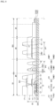
- FIG. 9 is a cross-sectional view of a display device according to another embodiment.
- a touch line TL_1 of a display device 2 according to the present embodiment differs from the display device 1 according to FIG. 6 in that it does not include the first touch line portion TL1.
- the touch line TL_1 may include the second touch line portion TL2 and the bending bridge electrode CL.
- a first touch conductive layer 220_1 may not include the first touch line portion TL1 of FIG. 6 .
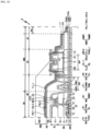
- FIG. 10 is a cross-sectional view of a display device according to still another embodiment.
- a display device 3 differs from the display device 1 according to FIG. 6 in that a second touch conductive layer 240_1 does not include the second touch line portion TL2 and the third touch pad portion TPAD3 and a first touch conductive layer 220_2 includes a first touch line portion TL1_1 and a third touch pad portion TPAD3_1.
- the upper surface of the second touch line portion TL2 of the display device 1 according to FIG. 6 is in direct contact with the touch organic layer 250.
- the corrosion of the second touch line portion TL2 may occur.
- by omitting the second touch line portion TL2, forming a touch line TL_2 through a first touch line portion TL1_1 and the bending bridge electrode CL, and arranging the touch insulating layer 230 between the first touch line portion TL1_1 and the touch organic layer 250 it is possible to minimize the permeation of moisture into the touch line TL_2.
Landscapes
- Engineering & Computer Science (AREA)
- General Engineering & Computer Science (AREA)
- Theoretical Computer Science (AREA)
- Human Computer Interaction (AREA)
- Physics & Mathematics (AREA)
- General Physics & Mathematics (AREA)
- Microelectronics & Electronic Packaging (AREA)
- Manufacturing & Machinery (AREA)
- Devices For Indicating Variable Information By Combining Individual Elements (AREA)
- Electroluminescent Light Sources (AREA)
Abstract
The disclosure relates to a display device. The display device according to one embodiment includes a base substrate including a display area including a plurality of pixels and a non-display area near the display area, a first dam disposed on the base substrate of the non-display area, a second dam disposed on the base substrate of the non-display area and disposed between the first dam and the display area, and a touch sensor layer including a touch conductive layer disposed on the first dam and the second dam and a touch organic layer on the touch conductive layer, wherein the touch organic layer ends inside the first dam, and the first dam and the second dam include the same material.
Description
- The present application claims priority to
Korean Patent Application No. 10-2023-0112495, filed August 28, 2023 - The present disclosure relates to a display device and a method of manufacturing the same.
- As the information society develops, various demands for display devices for displaying images are increasing, and various types of display devices such as liquid crystal display (LCD) devices and organic light emitting diode (OLED) display devices are utilized.
- A display device may include a display panel and a touch sensor layer, and the touch sensor layer may be attached to the display panel as a separate layer from the display panel, but may also be disposed directly on the display panel.
- Recently, when the display device including the display panel and the touch sensor layer is manufactured, efforts for reducing the number of masks are being made.
- The present disclosure is directed to providing a display device manufactured using a fewer number of masks.
- The objects of the present disclosure are not limited to the above-described object, and other technical objects may be inferred from embodiments below. At least one of these objects is solved by the subject-matter of the independent claim. Refinements are defined by the respective dependent claims.
- A display device according to one aspect of the present disclosure includes a base substrate including a display area including a plurality of pixels, and a non-display area near the display area, a first dam disposed on the base substrate of the non-display area, a second dam disposed on the base substrate of the non-display area and disposed between the first dam and the display area, and a touch sensor layer including a touch conductive layer disposed between the first dam and the second dam and a touch organic layer on the touch conductive layer, wherein the touch organic layer ends inside the first dam, and the first dam and the second dam include the same material.
- A display device according to another aspect of the present disclosure includes a display area including a plurality of pixels, and a non-display area located near the display area, wherein the non-display area includes a first dam part surrounding the display area, and a second dam part surrounding the display area and disposed between the first dam part and the display area, and the first dam part includes a main dam portion having a first separation distance to the second dam part, and a protruding dam portion having a second separation distance to the second dam part.
- A display device according to another aspect of the present disclosure comprises: a base substrate including a display area including a plurality of pixels, and a non-display area near or adjacent to the display area; a first dam disposed on the base substrate of the non-display area; a second dam disposed on the base substrate of the non-display area and disposed between the first dam and the display area. Furthermore, the display device may comprise a touch sensor layer including: a touch conductive layer disposed between the first dam and the second dam, and a touch organic layer on the touch conductive layer. The touch organic layer may end inside the first dam. The touch organic layer may have an end disposed on or inside or within the first dam. The first dam may surround the touch organic layer, in particular an end of the touch organic layer. The first dam and the second dam may include the same material.
- A display device according to another aspect of the present disclosure comprises: a display area including a plurality of pixels; and a non-display area located near the display area. The non-display area may include: a first dam part surrounding the display area; and a second dam part surrounding the display area and disposed between the first dam part and the display area. The first dam part may include: a main dam portion having a first separation distance to the second dam part; and a protruding dam portion having a second separation distance to the second dam part.
- A display device according to any aspect or embodiment of the present disclosure may include one or several of the following optional features.
- A height of the first dam may be greater than a surface height of the second dam. A height of an upper surface of the first dam may be greater than a surface height of an upper surface of the second dam, as measured from the base substrate.
- The display device may further comprise a thin film encapsulation layer between the first dam and the touch sensor layer. The thin film encapsulation layer may include a first encapsulation inorganic layer, and/or an encapsulation organic layer disposed on the first encapsulation inorganic layer, and/or a second encapsulation inorganic layer disposed on the encapsulation organic layer.
- The encapsulation organic layer may end inside the second dam. The encapsulation organic layer may have an end disposed on or inside or within the second dam. The second dam may surround the encapsulation organic layer, in particular an end of the encapsulation organic layer.
- The encapsulation organic layer may not overlap the first dam, in particular in a thickness direction of the display device.
- The non-display area may include a bending region in which the display device is bent in a thickness direction. The first dam may be disposed in the bending region. The second dam may be disposed between the bending region and the display area.
- The display device may further comprise an organic element layer disposed on the base substrate of the display area. The organic element layer may include an anode, a bank layer exposing a portion of an upper surface of the anode, an organic layer disposed on the exposed upper surface of the anode, and a cathode disposed on the organic layer.
- The first dam and the second dam may be disposed coplanar with the bank layer. An upper surface of the first is coplanar with an upper surface of the bank layer. An upper surface of the second dam is coplanar with a lower surface of the bank layer.
- The two or more first dams may be provided.
- The first dam may be disposed on a second interlayer insulating layer between the bank layer and the base substrate. The second interlayer insulating layer may be disposed on the base substrate in the non-display area. The second layer insulating layer may be further disposed in the display area between the bank layer and the base substrate.
- The first dam may be disposed on a planarization layer between the bank layer and the base substrate. The planarization layer may be disposed on the base substrate in the non-display area. The planarization layer may be further disposed in the display area between the bank layer and the base substrate.
- The planarization layer may be disposed between the second interlayer insulating layer and the bank layer. The first dam may be disposed on the second interlayer insulating layer and the planarization layer.
- The first dam part and/or the second dam part may each include a closed loop shape.
- The first dam part may further include a connection dam portion connecting the main dam portion with the protruding dam portion.
- The non-display area may further include a bending region in which the display device is bent in a thickness direction. The protruding dam portion may be disposed in the bending region.
- The second separation distance may be greater than the first separation distance.
- The first dam part may include the first dam. The second dam part may include the second dam.
- According to the embodiments, by omitting one of the plurality of touch organic layers of the conventional touch sensor layer, it is possible to reduce the number of masks and simplify the manufacturing of the display device.
- Meanwhile, the one touch organic layer includes a dam for preventing the overflow of the other organic layer to the pad part. According to the embodiments, since the one touch organic layer is omitted, the dam may be formed using at least one of the organic layers of the display panel. In other words, by forming the dam for simplifying the stacking structure of the display device and preventing the overflow of the other organic layer to the pad part using the at least one of the organic layers of the display panel, it is possible to prevent the overflow of the other touch organic layer to the pad part.
- According to the embodiments, by reducing the number of masks and simplifying the process when the display device is manufactured, it is possible to achieve the process optimization.
- However, the effects obtainable from the present disclosure are not limited to the above-described effects, and other effects that are not mentioned will be able to be clearly understood by those skilled in the art to which the present disclosure pertains from the following description.
-
-
FIG. 1 is a schematic cross-sectional view of a display device according to one embodiment. -
FIG. 2 is a plan view of the display device according toFIG. 1 . -
FIG. 3 is a cross-sectional view showing a bent state of the display device according toFIG. 1 . -
FIG. 4 is a more detailed plan view of the display device according toFIG. 2 . -
FIG. 5 is an enlarged plan view of area A ofFIG. 4 . -
FIG. 6 is a cross-sectional view along line I-I' inFIG. 2 . -
FIGS. 7 and8 are cross-sectional views for each operation of a process in a method of manufacturing the display device according to one embodiment. -
FIG. 9 is a cross-sectional view of a display device according to another embodiment. -
FIG. 10 is a cross-sectional view of a display device according to still another embodiment. - Hereinafter, embodiments will be described with reference to the accompanying drawings. In the disclosure, when a first component (or an area, a layer, a portion, or the like) is described as "on," "connected," or "coupled to" a second component, it means that the first component may be directly connected/coupled to the second component or a third component may be disposed therebetween.
- The same reference numerals indicate the same components. In addition, in the drawings, thicknesses, proportions, and dimensions of components are exaggerated for effective description of technical contents. The term "and/or" includes all one or more combinations that may be defined by the associated configurations.
- Terms such as first and second may be used to describe various components, but the components are not limited by the terms. The terms are used only for the purpose of distinguishing one component from another. For example, a first component may be referred to as a second component, and similarly, the second component may also be referred to as the first component without departing from the scopes of the embodiments. The singular expression includes the plural expression unless the context clearly dictates otherwise.
- Terms such as "under," "at a lower side," "above," and "at an upper side" are used to describe the relationship between the components illustrated in the drawings. The terms are relative concepts and are described with respect to directions marked in the drawings.
- It should be understood that term such as "includes" or "has" is intended to specify the presence of features, numbers, steps, operations, components, parts, or a combination thereof described in the disclosure and does not preclude the presence or addition possibility of one or more other features, numbers, steps, operations, components, parts, or combinations thereof in advance.
-
FIG. 1 is a schematic cross-sectional view of a display device according to one embodiment. - Referring to
FIG. 1 , adisplay device 1 according to one embodiment may include adisplay panel 100, and atouch sensor layer 200 formed on thedisplay panel 100. Thedisplay panel 100 may include a substrate part SUB, a circuit element layer CEL formed on the substrate part SUB, an organic element layer EL formed on the circuit element layer CEL, a thin film encapsulation layer TFE formed on the organic element layer EL, and thetouch sensor layer 200 formed on the thin film encapsulation layer TFE. In one embodiment, thedisplay panel 100 may be an organic light emitting display panel including the organic element layer EL. However, thedisplay panel 100 is not limited thereto and may be a liquid crystal display panel or an inorganic light emitting display panel. Hereinafter, an example in which thedisplay panel 100 is the organic light emitting display panel will be mainly described. - The
display device 1 may include a display area DA and a non-display area NDA near the display area DA. The display area DA may include a plurality of pixels to generate or display images. The non-display area NDA may not generate the images. The non-display area NDA may not include pixels, but is not limited thereto. The non-display area NDA may surround the display area DA. The non-display area may be arranged at a periphery of the display area DA. - The
display device 1 may further include a sensing area SA and a non-sensing area NSA near the sensing area SA. The sensing area SA and the non-sensing area NSA may correspond to the display area DA and the non-display area NDA, respectively, and may have the same area, but are not limited thereto. The sensing area SA may be an area in which touch electrodes TE and RE to be described below inFIG. 4 are disposed, and a touch line TL connected to the touch electrodes TE and RE, touch pads TPAD connected to the touch line TL, etc. may be disposed in the non-sensing area NSA. - The substrate part SUB, the circuit element layer CEL, the organic element layer EL, the thin film encapsulation layer TFE, and the
touch sensor layer 200 will be described below. -
FIG. 2 is a plan view of the display device according toFIG. 1 . - Referring to
FIG. 2 , a planar shape of the display area DA may have a rectangular shape. However, the present disclosure is not limited thereto, and the planar shape of the display area DA may be a square, circular, elliptical, or other polygonal shapes. For example, the display area DA may have a rectangular shape with rounded corners, but is not limited thereto and may also have a rectangular shape with angled corners. - In embodiments, a first direction DR1, also referred to as a horizontal direction, and a second direction DR2, also referred to as a vertical direction, are different directions and intersect each other, for example, directions that intersect vertically or perpendicularly in a plan view of the display device. A third direction DR3 (see
FIG. 3 ) is a direction that intersects the plane on which the first direction DR1 and the second direction DR2 are present when the display device is not bent, for example, a direction perpendicular to both the first direction DR1 and the second direction DR2. InFIG. 2 , in general, the first direction DR1 may be the same as extending directions of short sides of thedisplay panel 100, the second direction DR2 may the same as extending directions of long sides of thedisplay panel 100, and the third direction DR3 may be the same as a stacking direction of the substrate part SUB, the circuit element layer CEL, the organic element layer EL, thin film encapsulation layer TFE, and thetouch sensor layer 200 inFIG. 1 . However, the directions described in the embodiment should be understood as indicating relative directions, and the embodiment is not limited to the described direction. - The display area DA may include short sides extending in the first direction DR1 and long sides extending in the second direction DR2. The non-display area NDA may surround the display area DA. The non-display area NDA may be disposed at one , i.e. left, side and the other, i.e. right, side of the display area DA in the first direction DR1 and one, i.e. upper, side and the other, i.e. lower, side of the display area DA in the second direction DR2. Portions of the non-display area NDA may substantially form a ring. The non-display area NDA or portions thereof may surround the display area DA. The non-display area NDA or at least portions thereof may be arranged to be adjacent to the display area DA.
The non-display area NDA located at the other side of the display area DA in the second direction DR2 may extend further from a central portion of the one side of the display area DA in the second direction DR2 toward the other side in the second direction DR2. A width of the non-display area NDA in the first direction DR1 further extending from the central portion of the other side of the display area DA in the second direction DR2 toward the other side in the second direction DR2 may be smaller than a width of the non-display area NDA in the first direction DR1 adjacent to the other side of the display area DA in the second direction DR2. - The portion of the non-display area NDA arranged at the lower side of the display area DA may be wider than the portion of the non-display area NDA arranged at the upper side of the display area DA.
- The
display device 1 may include a main region MR, a sub-region SR, and a bending region BR between the main region MR and the sub-region SR. The display area DA and the portions of the non-display area NDA surrounding the display area DA on all four surfaces or sides of the display area DA form the main region MR. A portion extending from the central portion of the other side of the display area DA in the second direction DR2 toward the other side in the second direction DR2 may form the bending region BR and the sub-region SR. A portion of the non-display area NDA extending from the portion of the non-display area NDA arranged at the lower side of the non-display area may form the bending region BR and the sub-region SR. The main region MR may be arranged between the display area DA and the bending region BR. The main region MR, the bending region BR and the sub-region SR may be arranged at the lower side of the display area DA and/or may be arranged in this order starting from the display area DA against the second direction DR2. - The bending region BR may be disposed between the sub-region SR and the main region MR. The sub-region SR may include a first pad area PA1 and a second pad area PA2. The second pad area PA2 may be located at an end portion of the other side of the sub-region SR in the second direction DR2. The first pad area PA1 may be arranged to be adjacent to the bending region BR. The second pad area PA2 may be arranged to be adjacent to the first pad area PA1 and/or may extend away from the first pad area PA1 against the second direction DR2. The first pad area PA1 may be arranged between the bending region BR and the second pad area PA2.
- The
display device 1 may further include adata driver 300 and a printedcircuit board 500. Thedata driver 300 may be disposed in the first pad area PA1, and the printedcircuit board 500 may be attached to the second pad area PA2. A plurality of pads connected to thedata driver 300 and the printedcircuit board 500 may be disposed in each of the first pad area PA1 and the second pad area PA2. Thedata driver 300 may be formed, for example, in the form of a driving chip (IC), but is not limited thereto. In one embodiment, an example in which thedata driver 300 is disposed in a chip on plastic type that is directly mounted on thedisplay panel 100 is described, but the present disclosure is not limited thereto and is disposed in a chip on glass type or a chip on film type. - As described above in
FIG. 1 , the display area DA may include a plurality of pixels PX. The plurality of pixels PX may each be connected to a scan line SL and a data line DL. In addition to the scan line SL and the data line DL, the pixel PX may include and/or may be connected to a high voltage power line, a low voltage power line, or various lines in the art. the pixel PX may include a capacitor. - The
display device 1 according to one embodiment may further include a first dam part DP1 and a second dam part DP2. The first dam part DP1 and the second dam part DP2 may each surround the display area DA. The first dam part DP1 and the second dam part DP2 may each have a closed loop shape that fully surrounds the display area DA. The second dam part DP2 may be disposed between the first dam part DP1 and the display area DA. The second dam part DP2 may be disposed between the display area DA and the bending region BR to be described below. - The first dam part DP1 and the second dam part DP2 may each be disposed in the non-display area NDA. For example, the second dam part DP2 may be disposed in the non-display area NDA adjacent to the display area DA and disposed in the main region MR. The first dam part DP1 may be disposed outside the second dam part DP2, i.e. may surround the second dam part DP2. The first dam part DP1 may include a main dam portion DP1a, a protruding dam portion DP1b, and a connection dam portion DP1c. The main dam portion DP1a may be disposed at one side and the other side of the display area DA in the first direction DR1 and disposed in the non-display area NDA disposed adjacent to the one side of the display area DA in the second direction DR2. The main dam portion DP1a may be disposed at the periphery of the non-display area NDA adjacent to the other side of the display area DA in the second direction DR2.
- The main dam portion DP1a may be disposed in the non-display area NDA arranged at the one side and the other side of the display area DA in the first direction DR1. The main dam portion DP1a may be disposed in the non-display area NDA arranged at the one side of the display area DA in the second direction DR2. The main dam portion DP1a may be disposed in the non-display area NDA arranged at the other side of the display area DA in the second direction DR2.
- The main dam portion DP1a disposed in the non-display area NDA disposed adjacent to the one side and the other side of the display area DA in the first direction DR1 and the one side of the display area DA in the second direction DR2, and at the periphery of the non-display area NDA adjacent to the other side of the display area DA in the second direction DR2 may be formed integrally. The main dam portion DP1a may be disposed in the main region MR.
- The protruding dam portion DP1b may be disposed in the bending region BR and may not be disposed in the main region MR. The protruding dam portion DP1b may extend along the first direction DR1. The main dam portion DP1a disposed in the non-display area NDA arranged at the other side of the display area DA in the second direction DR2 may extend along the first direction DR1.
- The first dam part DP1 and the second dam part DP2 may be arranged to be spaced apart or separated from each other. In other words, the main dam portion DP1a and the second dam part DP2 may be disposed to have a first separation distance d1, and the protruding dam portion DP1b and the second dam part DP2 may be disposed to have a second separation distance d2 greater than the first separation distance d1. The main dam portion DP1a and the protruding dam portion DP1b may be connected through the connection dam portion DP1c. The connection dam portion DP1c may extend from the main region MR to the bending region BR. The connection dam portion DP1c may be disposed throughout the bending region BR and the main region MR, but is not limited thereto. In other words, when the protruding dam portion DP1b is disposed in the bending region BR adjacent to the boundary between the bending region BR and the main region MR, the connection dam portion DP1c may be disposed only in the main region MR.
- In some embodiments, the protruding dam portion DP1b may be disposed in the main region MR.
- In some embodiments, the second separation distance d2 may be equal to the first separation distance d1.
-
FIG. 3 is a cross-sectional view showing a bent state of the display device according toFIG. 1 . - Referring to
FIG. 3 , the bending region BR of thedisplay panel 100 of thedisplay device 1 according to one embodiment may be bent in the thickness direction (or the third direction DR3). Therefore, the main region MR and the sub-region SR may overlap each other in the thickness direction. Thedisplay panel 100 may be bent in such a way that a lower surface of the main region MR and an upper surface of the sub-region SR face each other. The printedcircuit board 500 may be attached to an end portion of the sub-region SR. -
FIG. 4 is a more detailed plan view of the display device according toFIG. 2 .FIG. 5 is an enlarged plan view of area A ofFIG. 4. FIG. 4 is a plan view of thedisplay device 1 according toFIG. 2 and specifically shows the touch sensor layer 200 (seeFIG. 1 ), and the touch line TL and the touch pad TPAD that are connected to thetouch sensor layer 200. - Referring to
FIGS. 4 and5 , thetouch sensor layer 200 may include a plurality of touch electrodes TE and RE for detecting the user's touch using a capacitance method, and the touch lines TL connecting the plurality of touch electrodes TE and RE with the touch pads TPAD. For example, thetouch sensor layer 200 may sense the user's touch using a self-capacitance method or a mutual capacitance method. - A plurality of touch electrodes TE and RE may be disposed in the sensing area SA.
- The plurality of touch electrodes TE and RE may generate a mutual capacitance or a self-capacitance to detect the touch of an object or a person. The plurality of touch electrodes TE and RE may include a plurality of driving electrodes TE 240_T and a plurality of detecting electrodes RE 240_R.
- The plurality of driving electrodes TE 240_T may be arranged in the first direction DR1 and the second direction DR2. The plurality of driving electrodes TE 240_T may be spaced apart from each other in the first direction DR1 and the second direction DR2. The driving electrodes TE 240_T adjacent to each other in the second direction DR2 may be electrically connected through and/or to a bridge electrode 220_B.
- The plurality of detecting electrodes RE 240_R may extend in the first direction DR1 and may be spaced apart from each other in the second direction DR2. The plurality of detecting electrodes RE 240_R may be arranged in the first direction DR1 and the second direction DR2. The detecting electrodes RE 240_R adjacent to each other in the first direction DR1 may be electrically connected through and/or to a connection part 240_B.
- The plurality of driving electrodes TE 240_T and detecting electrodes RE 240_R may each be connected to a plurality of touch pads TPAD through the touch lines TL.
- The bridge electrode 220_B may be disposed on a different layer from the plurality of driving electrodes TE 240_T and the plurality of detecting electrodes RE 240_R. The detecting electrodes RE 240_R adjacent to each other in the first direction DR1 may be electrically connected through the connection part 240_B formed on the same layer as the plurality of driving electrodes TE 240_T or the plurality of detecting electrodes RE 240_R, and the driving electrodes TE 240_T adjacent to each other in the second direction DR2 may be electrically connected through the bridge electrode 220_B formed on a different layer from the plurality of driving electrodes TE 240_T or the plurality of detecting electrodes RE 240_R.
- Therefore, even when the bridge electrode 220_B overlaps the plurality of detecting electrodes RE 240_R in the thickness direction DR3, the plurality of driving electrodes TE 240_T and the plurality of detecting electrodes RE 240_R may be insulated from each other. The mutual capacitance may be generated between the driving electrode TE 240_T and the detecting electrode RE 240_R.
-
FIG. 6 is a cross-sectional view along line I-I' inFIG. 2 . - Referring to
FIG. 6 , thedisplay device 1 may include the substrate part SUB, the circuit element layer CEL formed on the substrate part SUB, the organic element layer EL formed on the circuit element layer CEL, the thin film encapsulation layer TFE formed on the organic element layer EL, and thetouch sensor layer 200 formed on the thin film encapsulation layer TFE. - The substrate part SUB may include a
base substrate 101. Thebase substrate 101 may support layers disposed thereon. Thebase substrate 101 may be disposed throughout the display area DA and the non-display area NDA. Thebase substrate 101 may be made of an insulating material such as a polymer resin. Examples of the polymer material may include polyethersulphone (PES), polyacrylate (PA), polyarylate (PAR), polyetherimide (PEI), polyethylene napthalate (PEN), polyethylene terepthalate (PET), polyphenylene sulfide (PPS), polyallylate, polyimide (PI), polycarbonate (PC), cellulose triacetate (CAT), cellulose acetate propionate (CAP), or combinations thereof. Thebase substrate 101 may be a flexible substrate capable of bending, folding, rolling, etc. An example of a material forming the flexible substrate may be polyimide (PI), but is not limited thereto. Thebase substrate 101 may be a rigid substrate made of glass, quartz, etc. - The circuit element layer CEL may be formed on the substrate part SUB. The circuit element layer CEL may include a
semiconductor layer 105, agate insulating layer 111 formed on thesemiconductor layer 105, a gate conductive layer including a gate electrode GE on thegate insulating layer 111, a firstinterlayer insulating layer 112 formed on the gate conductive layer, a first source drain conductive layer 130 including asource electrode 131, adrain electrode 133, and a first touch pad portion TPAD1 of a touch pad TPAD, a secondinterlayer insulating layer 141 formed on the first source drain conductive layer 130, a second source drainconductive layer 150 including aconnection electrode 151 formed on the secondinterlayer insulating layer 141, a second touch pad portion TPAD2 of the touch pad TPAD, and a bending bridge electrode CL, and a firstorganic layer 160 including aplanarization layer 161 formed on the second source drainconductive layer 150 and a second lower dam DAM21. - The organic element layer EL may include an organic light emitting diode OLED including an anode ANO formed on the first
organic layer 160, an organic layer OL, and a cathode electrode CAT, and a secondorganic layer 170 including abank layer 171, a second upper dam DAM22, and a first dam DAM1. - The thin film encapsulation layer TFE may include a first encapsulation
inorganic layer 181 formed on the organic element layer EL, an encapsulationorganic layer 182 formed on the first encapsulationinorganic layer 181, and a second encapsulationinorganic layer 183 formed on the encapsulationorganic layer 182. - The
touch sensor layer 200 may include atouch buffer layer 210 formed on the thin film encapsulation layer TFE, a first touchconductive layer 220 including the bridge electrode 220_B formed on thetouch buffer layer 210 and a first touch line portion TL1 of the touch line TL, a touchinsulting layer 230 formed on the first touchconductive layer 220, a second touchconductive layer 240 including a driving electrode 240_T formed on thetouch insulating layer 230, a second touch line portion TL2 of the touch line TL, and a third touch pad portion TPAD3 of the touch pad TPAD, and a touchorganic layer 250 formed on the second touchconductive layer 240. - A buffer layer may be disposed on the
base substrate 101. The buffer layer can prevent the diffusion of impurity ions and prevent the permeation of moisture or outside air. - Unlike shown, the buffer layer may include a plurality of layers. In other words, the buffer layer may be provided as layers formed by alternately stacking silicon nitride (SiNx) and silicon oxide (SiOx) at least once.
- The
semiconductor layer 105 may be disposed in the display area DA on the buffer layer. Thesemiconductor layer 105 may include polycrystalline silicon. Thesemiconductor layer 105 may include a channel area, a source area, and a drain area. The polycrystalline silicon may be formed by crystallizing amorphous silicon. Examples of the crystallization methods may include a rapid thermal annealing (RTA) method, a solid phase crystallization (SPC) method, an excimer laser annealing (ELA) method, a metal induced crystallization (MIC) method, a metal induced lateral crystallization (MILC) method, a sequential crystallization (SLS) method, etc., but are not limited thereto. - The
gate insulating layer 111 may be formed on thesemiconductor layer 105. Thegate insulating layer 111 may be generally disposed throughout the display area DA and the non-display area NDA. Thegate insulating layer 111 may be a gate insulating film having a gate insulating function. Thegate insulating layer 111 may include a silicon compound, metal oxide, etc. For example, thegate insulating layer 111 may include silicon oxide, silicon nitride, silicon oxynitride, aluminum oxide, tantalum oxide, hafnium oxide, zirconium oxide, titanium oxide, etc. The materials may be used alone or in combination. Although the drawing shows that thegate insulating layer 111 is formed of a single film, in some cases, thegate insulating layer 111 may be a multilayered film formed of stacked films made of different materials. - The gate conductive layer may be disposed on the
gate insulating layer 111. - In one embodiment, the gate conductive layer may include the gate electrode GE. In addition, the gate conductive layer may further include a scan signal line that transmits a scan signal to the gate electrode GE. The gate electrode GE may be disposed to overlap the channel area of the
semiconductor layer 105. - The gate conductive layer may include one or more selected from molybdenum (Mo), aluminum (Al), platinum (Pt), palladium (Pd), silver (Ag), magnesium (Mg), gold (Au), nickel (Ni), neodymium (Nd), iridium (Ir), chromium (Cr), calcium (Ca), titanium (Ti), tantalum (Ta), tungsten (W), and copper (Cu). In addition, although the drawing shows only the case where the gate conductive layer is a single layer, in some cases, the gate conductive layer may be formed as a multilayered layer. In this case, the multilayered film of the gate conductive layer may be formed as a stacked film made of different metals among the above-described metals.
- The first
interlayer insulating layer 112 may be disposed on the gate conductive layer. The firstinterlayer insulating layer 112 may be disposed throughout the display area DA and the non-display area NDA. - The first
interlayer insulating layer 112 may insulate the gate conductive layer and the first source drain conductive layer 130. The firstinterlayer insulating layer 112 may be an interlayer insulating film. - The first
interlayer insulating layer 112 may include an inorganic insulating material such as silicon oxide, silicon nitride, silicon oxynitride, hafnium oxide, aluminum oxide, titanium oxide, tantalum oxide, or zinc oxide, or an organic insulating material such as a polyacrylates resin, an epoxy resin, a phenolic resin, a polyamides resin, a polyimides rein, an unsaturated polyesters resin, a polyphenylenethers resin, a polyphenylenesulfides resin or benzocyclobutene (BCB). In the drawing, although an example in which the firstinterlayer insulating layer 112 is the single layer is shown, the present disclosure is not limited thereto and may be a multilayered layer formed of a stacked layer containing different materials. - The first source drain conductive layer 130 may be disposed on the first
interlayer insulating layer 112. The first source drain conductive layer 130 may include thesource electrode 131, thedrain electrode 133, and the first touch pad portion TPAD1. Thesource electrode 131 may be connected to the source area of thesemiconductor layer 105, and thedrain electrode 133 may be connected to the drain area of thesemiconductor layer 105. The first touch pad portion TPAD1 may be disposed in the second pad area PA2. The first source drain conductive layer 130 may include aluminum (Al), copper (Cu), titanium (Ti), etc., and may be formed as a multilayered or single layer. In one embodiment, the first source drain conductive layer 130 may have a multilayered structure of Ti/Al/Ti, but is not limited thereto. Thesource electrode 131, thedrain electrode 133, and the first touch pad portion TPAD1 include the same material and may be formed in the same process. - The second
interlayer insulating layer 141 may be disposed on the first source drain conductive layer 130. The secondinterlayer insulating layer 141 may be disposed in the display area DA and the non-display area NDA. In the non-display area NDA, the secondinterlayer insulating layer 141 may be disposed in the bending region BR and may also be disposed in portions of the main region MR and the sub-region SR that are adjacent to the bending region BR. The secondinterlayer insulating layer 141 may include an organic material such as an polyacrylates resin, an epoxy resin, a phenolic resin, a polyamides resin, a polyimides rein, an unsaturated polyesters resin, a poly phenylenethers resin, a polyphenylenesulfides resin, or benzocyclobutene (BCB). - The second source drain
conductive layer 150 may be disposed on the secondinterlayer insulating layer 141. The second source drainconductive layer 150 may include theconnection electrode 151 connected to thedrain electrode 133, the second touch pad portion TPAD2 disposed on the first touch pad portion TPAD1 and directly disposed on the first touch pad portion TPAD1, and the bending bridge electrode CL connected to the touch line TL at the periphery of the bending region BR and passing through the bending region BR. The second source drainconductive layer 150 may include aluminum (Al), copper (Cu), titanium (Ti), etc., and may be formed as a multilayered or single layer. In one embodiment, the second source drainconductive layer 150 may have a multilayered structure of Ti/Al/Ti, but is not limited thereto. Theconnection electrode 151, the second touch pad portion TPAD2, and the bending bridge electrode CL may include the same material and may be formed in the same process. - The first
organic layer 160 may be disposed on the second source drainconductive layer 150. The firstorganic layer 160 may include theplanarization layer 161 and the second lower dam DAM21. - The first
organic layer 160 may include an organic material such as a polyacrylates resin, an epoxy resin, a phenolic resin, a polyamides resin, a polyimides rein, an unsaturated polyesters resin, a poly phenylenethers resin, a polyphenylenesulfides resin, or benzocyclobutene (BCB). Theplanarization layer 161 and the second lower dam DAM21 may include the same material and may be formed in the same process. - The
planarization layer 161 may be disposed in the display area DA, the bending region BR, and the sub-region SR. In the display area DA, theplanarization layer 161 may be disposed on theconnection electrode 151 and the secondinterlayer insulating layer 141. In the bending region BR, theplanarization layer 161 may be disposed on the bending bridge electrode CL and the secondinterlayer insulating layer 141. In the sub-region SR, theplanarization layer 161 may be disposed on the firstinterlayer insulating layer 112. - The second lower dam DAM21 may form the second dam DAM2 together with the second upper dam DAM22.
- The anode ANO may be disposed on the
planarization layer 161 in the display area DA. The anode ANO may pass through theplanarization layer 161 and may be electrically connected to theconnection electrode 151. Theconnection electrode 151 may electrically connect the anode ANO with thedrain electrode 133. - The second
organic layer 170 may be disposed on the anode ANO. The secondorganic layer 170 may include thebank layer 171, the second upper dam DAM22, and the first dam DAM1. - The second
organic layer 170 may include an organic material such as an polyacrylates resin, an epoxy resin, a phenolic resin, a polyamides resin, a polyimides rein, an unsaturated polyesters resin, a poly phenylenethers resin, a polyphenylenesulfides resin, or benzocyclobutene (BCB). Thebank layer 171, the second upper dam DAM22, and the first dam DAM1 may include the same material and may be formed in the same process. - The
bank layer 171 may be disposed in the display area DA and may expose a portion of an upper surface of the anode ANO. Thebank layer 171 can define an emission area by exposing a central portion of the upper surface of the anode ANO. In the display area DA, an area in which thebank layer 171 is disposed can be defined as a non-emission area. - The second upper dam DAM22 may be disposed on a second lower dam DMA21. The second upper dam DAM22 may overlap the second lower dam DAM21 in the thickness direction. A width of the second upper dam DAM22 may be greater than a width of the second lower dam DAM21, and the second upper dam DAM22 may cover side surfaces of the second lower dam DAM21.
- The second dam DAM2 may include the second lower dam DAM21 and the second upper dam DAM22, and one or more second dams DAM2 may be provided. In
FIG. 6 , an example in which two second dams DAM2 are provided is shown. Two or more second dams DAM2 may be disposed to be spaced apart from each other. One or more second dams DAM2 may be disposed in the second dam part DP2. The one or more second dams DAM2 may form at least a portion of the second dam part DP2. The second dam DAM2 can prevent the encapsulationorganic layer 182 of the thin film encapsulation layer TFE to be described below from overflowing into the bending region BR. For example, the encapsulationorganic layer 182 may end at the second dam DAM2 located externally, as viewed from the display area DA, among the two second dams DAM2. Therefore, the encapsulationorganic layer 182 does not extend to the bending region BR and may not overlap at all with components located in the bending region BR. The encapsulationorganic layer 182 may not overlap the first dam DAM1. - The first dam DAM1 may be disposed in the bending region BR. The first dam DAM1 may be disposed in the first dam part DP1. The first dam DAM1 may form at least a portion of the first dam part DP1. One or more first dams DAM1 may be provided. In
FIG. 6 , an example in which two first dams DAM1 are provided has been shown. Two or more first dams DAM1 may be disposed in the first dam part DP1. The two or more first dams DAM1 may form at least a portion of the first dam part DP1. The first dam DAM1 can prevent the touchorganic layer 250 to be described below from overflowing into the sub-region SR. For example, the touchorganic layer 250 may end at and/or on and/or inside the first dam DAM1 located externally, as viewed from the display area DA, among the two first dams DAM1. The touchorganic layer 250 may be disposed on the internal first dam DAM1, as viewed from the display area DA. The end of the touchorganic layer 250 may be disposed on or inside or within the external first dam DAM1. The touchorganic layer 250, in particular an end of the touchorganic layer 250, may be surrounded by the external first dam DAM1. Hence, the touchorganic layer 250 may be disposed only within the (external) first dam DAM1 and/or may be surrounded by the (external) first dam DAM1 and/or may not be disposed outside the (external) first dam DAM1. Therefore, the touchorganic layer 250 does not extend to the sub-region SR and may not overlap at all with the components located in the sub-region SR. The first dam DAM1 may be disposed on the secondinterlayer insulating layer 141 and theplanarization layer 161. The first dam DAM1 may be disposed to overlap the secondinterlayer insulating layer 141 and theplanarization layer 161. - In some embodiments, a spacer may be further disposed on the second
organic layer 170. The spacer may include at least one of the exemplified materials of the secondorganic layer 170. In some embodiments, at least one of the first dam DAM1 and the second dam DAM2 may be formed to further include the spacer. For example, the first dam DAM1 may have a structure in which the spacer is stacked on the first dam DAM1 ofFIG. 6 , and the second dam DAM2 may have a structure in which the second lower dam DAM21, the second upper dam DAM22, and the spacer are stacked. - For example, the first dam DAM1 and the second dam DAM2 may have various stacking structures. In some embodiments, the first dam DAM1 may have a structure in which the first dam DAM1 of
FIG. 6 and theplanarization layer 161 disposed thereunder are stacked. In this case, theplanarization layer 161 may be patterned like the first dam DAM1, and the patternedplanarization layer 161 may be stacked with the first dam DAM1 ofFIG. 6 to form the first dam. - In some embodiments, the second dam DAM2 does not include the second lower dam DAM21 and may be formed only as the second upper dam DAM22.
- In some embodiments, the second dam DAM2 does not include the second upper dam DAM22 and may be formed only as the second lower dam DAM21.
- An upper surface of the first dam DAM1 may have a first surface height H1, as measured from the
base substrate 101, and an upper surface of the second dam DAM2 may have a second surface height H2, as measured from thebase substrate 101. The first surface height H1 may be greater than the second surface height H2. The first surface height H1 may be greater than the second surface height H2 by the thickness of the first dam DAM1, but is not limited thereto. - The organic layer OL may be disposed on the upper surface of the anode ANO and in an opening of the
bank layer 171. In the drawing, although an example in which the organic layer OL is disposed only in the opening of thebank layer 171 is described, the present disclosure is not limited thereto and may be disposed to extend from the opening of thebank layer 171 to an upper surface of thebank layer 171. - The organic layer OL may include an organic light emitting layer, a hole injection/transport layer, and an electron injection/transport layer.
- The cathode CAT is disposed on the organic layer OL and the
bank layer 171. The cathode CAT may be a common electrode disposed throughout a plurality of pixels PX in the display area DA. The organic layer OL, the anode ANO, and the cathode CAT may form the organic light emitting diode OLED. - The thin film encapsulation layer TFE is disposed on the cathode CAT. The thin film encapsulation layer TFE may cover the organic light emitting diode OLED. The thin film encapsulation layer TFE may be a stacking film formed by alternately stacking inorganic films and organic films. For example, the thin film encapsulation layer TFE may include the first encapsulation
inorganic layer 181, the encapsulationorganic layer 182, and the second encapsulationinorganic layer 183 that are stacked sequentially. The encapsulationinorganic layers organic layer 182 may include an organic material. The encapsulationorganic layer 182 may not overflow into the bending region BR by the second dam DAM2 and may end inside the second dam DAM2. The encapsulationorganic layer 182 may be disposed on the internal second dam DAM2, as viewed from the display area DA. The end of the encapsulationorganic layer 182 may be disposed on or inside or within the external second dam DAM2. The encapsulationorganic layer 182 , in particular an end of the encapsulationorganic layer 182, may be surrounded by the external second dam DAM2. Hence, the encapsulationorganic layer 182 may be disposed only within the (external) second dam DAM2 and/or may be surrounded by the (external) second dam DAM2 and/or may not be disposed outside the (external) second dam DAM2. In the second dam part DP2, the second encapsulationinorganic layer 183 may be in direct contact with the first encapsulationinorganic layer 181. For example, since the encapsulationorganic layer 182 ends inside the second dam DAM2, the encapsulationorganic layer 182 may not be disposed on the second dam DAM2. On the second dam DAM2, the second encapsulationinorganic layer 183 may be in direct contact with the first encapsulationinorganic layer 181. - The encapsulation
inorganic layers inorganic layers - The
touch sensor layer 200 may be disposed on the thin film encapsulation layer TFE. Thetouch buffer layer 210 may be disposed on the second encapsulationinorganic layer 183. - The
touch sensor layer 200 may be disposed on the second encapsulationinorganic layer 183. - The
touch buffer layer 210 can block a chemical solution (developer, etchant, etc.) used in the manufacturing process of the electrodes 240_T and 240_R disposed on thetouch buffer layer 210 or moisture from the outside from permeating the organic light emitting diode OLED including the organic layer. Therefore, thetouch buffer layer 210 can prevent damage to the organic light emitting diode OLED vulnerable to a chemical solution or moisture. Thetouch buffer layer 210 may include an inorganic material or an organic material. Thetouch buffer layer 210 may extend from the display area DA to the bending region BR and the sub-region SR and may expose the second touch pad portion TPAD2 in the second pad area PA2. - The first touch
conductive layer 220 may be disposed on thetouch buffer layer 210. The first touchconductive layer 220 may include the bridge electrode 220_B and the first touch line portion TL1. The bridge electrode 220_B may be disposed in the sensing area SA (or the display area DA) to electrically connect the driving electrodes 240_T adjacent to each other. The bridge electrode 220_B may be insulated with the connection part 240_B and thetouch insulating layer 230 interposed therebetween. - In
FIG. 6 , although an example in which the bridge electrode 220_B electrically connects the driving electrodes 240_T adjacent to each other is shown, the present disclosure is not limited thereto, and the bridge electrode 220_B may electrically connect the detecting electrodes 240_R adjacent to each other, and the connection part 240_B may electrically connect the driving electrodes 240_T adjacent to each other. - The first touch line portion TL1 may be disposed in the display area DA and the non-display area NDA. The first touch line portion TL1 may be electrically connected to the detecting electrode 240_R or the driving electrode 240_T. The first touch
line portion TL 1 may pass through or over the second dam part DP2 and extend to the bending region BR. The first touch line portion TL1 may form the touch line TL together with the second touch line portion TL2 and serve to electrically connect the electrodes 240_T and 240_R with the touch pad TPAD. - The
touch insulating layer 230 may be disposed on the first touchconductive layer 220. Thetouch insulating layer 230 may include an inorganic material. Thetouch insulating layer 230 may extend from the display area DA to the bending region BR and the sub-region SR and expose the second touch pad portion TPAD2 in the second pad area PA2. - The second touch
conductive layer 240 may be disposed on thetouch insulating layer 230. The second touchconductive layer 240 may include the driving electrode 240_T, the second touch line portion TL2, and the third touch pad portion TPAD3. - The second touch line portion TL2 may include a 2-1 touch line portion TL2a and a 2-2 touch line portion TL2b. The 2-1 touch line portion TL2a may overlap the first touch line portion TL1 in the thickness direction. The 2-1 touch line portion TL2a may be disposed in portions of the main region MR and the bending region BR. The 2-1 touch line portion TL2a may be electrically connected to the first touch line portion TL1 through a third contact hole CT3 passing through the
touch insulating layer 230 in the thickness direction. The 2-1 touch line portion TL2a may be electrically connected to the first touch line portion TL1 through the third contact hole CT3 passing through thetouch insulating layer 230 in the thickness direction, thereby reducing the resistance of the touch line TL. - The third contact hole CT3 may be located on the second dam part DP2, but is not limited thereto. The 2-1 touch line portion TL1a may be electrically connected to the bending bridge electrode CL in the bending region BR. The 2-1 touch line portion TL1a may be electrically connected to the bending bridge electrode CL through the first contact hole CT1 passing through the
touch insulating layer 230, thetouch buffer layer 210, the second encapsulationinorganic layer 183, the first encapsulationinorganic layer 181, and theplanarization layer 161. - The first contact hole CT1 may be disposed in the bending region BR, but may not be limited thereto. The first contact hole CT1 may be disposed between the second dam DAM2 and the first dam DAM1. The 2-2 touch line portion TL2b may be disposed in a portion of the bending region BR and the sub-region SR. The 2-2 touch line portion TL2b may be electrically connected to the bending bridge electrode CL in the bending region BR. The 2-2 touch line portion TL1b may be electrically connected to the bending bridge electrode CL through the second contact hole CT2 passing through the
touch insulating layer 230, thetouch buffer layer 210, the second encapsulationinorganic layer 183, the first encapsulationinorganic layer 181, and theplanarization layer 161. - The second contact hole CT2 may be disposed in the bending region BR, but may not be limited thereto. The second contact hole CT2 may be disposed between the first dam DAM1 and the touch pad TPAD.
- The touch line TL according to one embodiment may include the first touch line portion TL1, the second touch line portion TL2, and the bending bridge electrode CL. The touch line TL may include the bending bridge electrode CL made of a flexible material compared to the first and second touch line portions TL1 and TL2 in the bending region BR, thereby preventing the disconnection or cracks of the touch line TL due to bending.
- The 2-2 touch line portion TL2b may be connected to the third touch pad portion TPAD3 in the second pad area PA2. The third touch pad portion TPAD3 may overlap the second touch pad portion TPAD2 in the thickness direction and may be directly disposed on the second touch pad portion TPAD2. The third touch pad portion TPAD3 may be disposed both on an upper surface and side surfaces of the second touch pad portion TPAD2. The third touch pad portion TPAD3 may be in direct contact with an outer portion of the upper surface of the first touch pad portion TPAD1 exposed by the second touch pad portion TPAD2, but is not limited thereto.
- The touch
organic layer 250 may be disposed on the second touchconductive layer 240. The touchorganic layer 250 may be formed on the second touchconductive layer 240 using an inkjet method. In the process of forming the touchorganic layer 250 on the second touchconductive layer 240 using the inkjet method, the touchorganic layer 250 may overflow the sub-region SR, and to prevent the same, the second dam DAM2 and other dams may be additionally needed. Conventionally, a separate organic layer was used between the touchorganic layer 250 and the second touchconductive layer 240 to form a dam for preventing the overflowing of the touchorganic layer 250 in the first dam part DP1. - However, in this case, a process of the
display device 1 was complicated because a process of forming the separate organic layer and a process of forming the dam using the separate organic layer as a mask were added. However, according to thedisplay device 1 according to one embodiment, since the first dam DAM1 is formed together without forming the separate organic layer in the process of forming the second upper dam DAM22 of the second dam DAM2, the process of forming the separate organic layer and the process of forming the dam using the separate organic layer as the mask can be omitted. Therefore, it is possible to reduce the number of masks and simplify the manufacturing of thedisplay device 1. The touchorganic layer 250 may be disposed in the main region MR and the bending region BR and may end inside the first dam DAM1, when viewed from the display area DA. - Hereinafter, the method of manufacturing the
display device 1 will be described. When the method of manufacturing the display device according toFIGS. 7 and8 is described, the description will be made with reference toFIG. 6 together. When the method of manufacturing the display device based onFIGS. 7 and8 is described, overlapping descriptions of the components of thedisplay device 1 already described inFIG. 6 may be omitted, and operations of manufacturing the already described components of thedisplay device 1 may be performed in the stacking order of thedisplay device 1. -
FIGS. 7 and8 are cross-sectional views for each operation of a process in a method of manufacturing the display device according to one embodiment. - Referring to
FIGS. 6 to 8 , first, as shown inFIG. 7 , the firstorganic layer 160 is formed on the second source drainconductive layer 150. The firstorganic layer 160 may include theplanarization layer 161 and the second lower dam DAM21. - The first
organic layer 160 may include an organic material such as an polyacrylates resin, an epoxy resin, a phenolic resin, a polyamides resin, a polyimides rein, an unsaturated polyesters resin, a poly phenylenethers resin, a polyphenylenesulfides resin, or benzocyclobutene (BCB). Theplanarization layer 161 and the second lower dam DAM21 may include the same material and may be formed in the same process. - The
planarization layer 161 may be disposed in the display area DA, the bending region BR, and the sub-region SR. In the display area DA, theplanarization layer 161 may be disposed on theconnection electrode 151 and the secondinterlayer insulating layer 141. In the bending region BR, theplanarization layer 161 may be disposed on the bending bridge electrode CL and the secondinterlayer insulating layer 141. In the sub-region SR, theplanarization layer 161 may be disposed on the firstinterlayer insulating layer 112. - The second lower dam DAM21 may form a second dam DAM2 together with the second upper dam DAM22.
- As shown in
FIG. 8 , after the firstorganic layer 160 is formed, the secondorganic layer 170 is formed. - The second
organic layer 170 may include an organic material such as an polyacrylates resin, an epoxy resin, a phenolic resin, a polyamides resin, a polyimides rein, an unsaturated polyesters resin, a poly phenylenethers resin, a polyphenylenesulfides resin, or benzocyclobutene (BCB). The secondorganic layer 170 may be formed by thebank layer 171, the second upper dam DAM22, and the first dam DAM1. Thebank layer 171, the second upper dam DAM22, and the first dam DAM1 may include the same material and may be formed in the same process. - The
bank layer 171 may be disposed in the display area DA and may expose a portion of an upper surface of the anode ANO. Thebank layer 171 can define an emission area by exposing a central portion of the upper surface of the anode ANO. In the display area DA, an area in which thebank layer 171 is disposed can be defined as a non-emission area. - The second upper dam DAM22 may be disposed on a second lower dam DMA21. The second upper dam DAM22 may overlap the second lower dam DAM21 in the thickness direction. A width of the second upper dam DAM22 may be greater than a width of the second lower dam DAM21, and the second upper dam DAM22 may cover side surfaces of the second lower dam DAM21. The second upper dam DAM22 may be formed together with the
bank layer 171. - The second dam DAM2 may include the second lower dam DAM21 and the second upper dam DAM22, and one or more second dams DAM2 may be provided. In
FIG. 6 , an example in which two second dams DAM2 are provided has been shown. Two or more second dams DAM2 may be disposed to be spaced apart from each other. Two or more second dams DAM2 may be disposed in the second dam part DP2. The second dam DAM2 can prevent the encapsulationorganic layer 182 of the thin film encapsulation layer TFE from overflowing into the bending region BR. For example, the encapsulationorganic layer 182 may end at the second dam DAM2 located externally among the two second dams DAM2. Therefore, the encapsulationorganic layer 182 does not extend to the bending region BR and may not overlap at all with components located in the bending region BR. - The first dam DAM1 may be disposed in the bending region BR. The first dam DAM1 may be disposed in the first dam part DP1. One or more first dams DAM1 may be provided. In
FIG. 6 , an example in which two first dams DAM1 are provided has been shown. One or more first dams DAM1 may be disposed in the first dam part DP1. The first dam DAM1 can prevent the touchorganic layer 250 from overflowing into the sub-region SR. For example, the touchorganic layer 250 may end at the first dam DAM1 located externally among the two first dams DAM1. Therefore, the touchorganic layer 250 does not extend to the sub-region SR and may not overlap at all with the components located in the sub-region SR. The first dam DAM1 may be formed together with thebank layer 171. - Hereinafter, other embodiments of the display device will be described. Hereinafter, in embodiments, overlapping descriptions of the components of the
display device 1 already described inFIG. 6 can be omitted. -
FIG. 9 is a cross-sectional view of a display device according to another embodiment. - Referring to
FIG. 9 , a touch line TL_1 of a display device 2 according to the present embodiment differs from thedisplay device 1 according toFIG. 6 in that it does not include the first touch line portion TL1. - More specifically, the touch line TL_1 may include the second touch line portion TL2 and the bending bridge electrode CL. A first touch conductive layer 220_1 may not include the first touch line portion TL1 of
FIG. 6 . - Since the remaining descriptions are as described above in
FIG. 6 , detailed descriptions thereof will be omitted. -
FIG. 10 is a cross-sectional view of a display device according to still another embodiment. - Referring to
FIG. 10 , a display device 3 according to the present embodiment differs from thedisplay device 1 according toFIG. 6 in that a second touch conductive layer 240_1 does not include the second touch line portion TL2 and the third touch pad portion TPAD3 and a first touch conductive layer 220_2 includes a first touch line portion TL1_1 and a third touch pad portion TPAD3_1. - More specifically, the upper surface of the second touch line portion TL2 of the
display device 1 according toFIG. 6 is in direct contact with the touchorganic layer 250. In other words, when moisture enters the second touch line portion TL2 through the touchorganic layer 250, the corrosion of the second touch line portion TL2 may occur. However, according to the present embodiment, by omitting the second touch line portion TL2, forming a touch line TL_2 through a first touch line portion TL1_1 and the bending bridge electrode CL, and arranging thetouch insulating layer 230 between the first touch line portion TL1_1 and the touchorganic layer 250, it is possible to minimize the permeation of moisture into the touch line TL_2. - Since the remaining descriptions are as described above in
FIG. 6 , detailed descriptions thereof will be omitted. - Although the embodiments have been described above with reference to the accompanying drawings, those skilled in the art to which the present disclosure pertains will be able to understand that the above-described technical configuration can be carried out in other specific forms without changing essential features thereof. Therefore, it should be understood that the above-described embodiments are illustrative and not restrictive in all respects. In addition, the scope of the present disclosure is described by the claims to be described below rather than the detailed description. In addition, the meaning and scope of the claims and all changed or modified forms derived from the equivalent concept should be construed as being included in the scope of the present disclosure.
-
- 1: display device
- 100: display panel
- 200: touch sensor layer
- SUB: substrate part
- CEL: circuit element layer
- EL: organic element layer
- TFE: thin film encapsulation layer
Claims (15)
- A display device (1) comprising:a base substrate (101) including a display area (DA) including a plurality of pixels (PX), and a non-display area (NDA) adjacent to the display area (DA);at least one first dam (DAM1) disposed on the base substrate in the non-display area (NDA);at least one second dam (DAM2) disposed on the base substrate in the non-display area and disposed between the first dam and the display area; anda touch sensor layer (200) including:a touch conductive layer (220) disposed to extend between the first dam and the second dam, anda touch organic layer (250) on the touch conductive layer (220),wherein the touch organic layer (250) ends on or inside the at least one first dam (DAM1), andwherein the first dam and the second dam include the same material.
- The display device of claim 1, wherein a height of an upper surface of the first dam is greater than a height of an upper surface of the second dam, as measured from the base substrate.
- The display device of any one of the preceding claims, further comprising a thin film encapsulation layer (TFE) between the first dam and the touch sensor layer,
wherein the thin film encapsulation layer includes a first encapsulation inorganic layer (181), an encapsulation organic layer (182) disposed on the first encapsulation inorganic layer, and a second encapsulation inorganic layer (183) disposed on the encapsulation organic layer. - The display device of claim 3, wherein the encapsulation organic layer (182) ends on or inside the at least one second dam (DAM2), and/or
wherein the first encapsulation inorganic layer (181) and the second encapsulation inorganic layer (183) are arranged between the first end of the touch organic layer (250) and the first dam (DAM1). - The display device of claim 4, wherein the encapsulation organic layer (183) does not overlap the first dam (DAM1) in a thickness direction (DR3) of the display device.
- The display device of any one of the preceding claims, wherein the non-display area (NDA) includes a bending region (BR) in which the display device is bent in a thickness direction (DR3), the first dam (DAM1) is disposed in the bending region, and the second dam (DAM2) is disposed between the bending region and the display area.
- The display device of any one of the preceding claims, further comprising an organic element layer (EL) disposed on the base substrate in the display area, wherein the organic element layer includes an anode (ANO), a bank layer (171) exposing a portion of an upper surface of the anode, an organic layer (OL) disposed on the exposed upper surface of the anode, and a cathode (CAT) disposed on the organic layer.
- The display device of claim 7, wherein an upper surface of the first dam (DAM1) is coplanar with an upper surface of the bank layer (171), and/or wherein an upper surface of the second dam (DAM2) is coplanar with a lower surface of the bank layer (171).
- The display device of claim 7 or 8, wherein the first dam is disposed on a second interlayer insulating layer (141) disposed on the base substrate (101) in the non-display area (NDA),
wherein the second layer insulating layer (141) is further disposed in the display area (DA) between the bank layer (171) and the base substrate (101). - The display device of claim 7, 8 or 9, wherein the first dam (DAM1) is disposed on a planarization layer (161) disposed on the base substrate (101) in the non-display area (NDA),
wherein the planarization layer (161) is further disposed in the display area (DA) between the bank layer (171) and the base substrate (101). - The display device of claim 10, wherein the planarization layer (161) is disposed between the second interlayer insulating layer (141) and the bank layer (171).
- The display device of any one of the preceding claims, wherein two or more first dams (DAM1) are provided.
- The display device of any one of the preceding claims, wherein the non-display area includes:a first dam part (DP1) surrounding the display area (DA), including the at least one first dam (DAM1); anda second dam part (DP2) surrounding the display area and disposed between the first dam part (DP1) and the display area (DA), including the at least one second dam (DAM2), andwherein the first dam part (DP1) includes:a main dam portion (DP1a) having a first separation distance (d1) to the second dam part (DP2); anda protruding dam portion (DP1c) having a second separation distance (d2) to the second dam part (DP2)wherein the second separation distance is greater than the first separation distance.
- The display device of claim 13, wherein the first dam part and the second dam part each include a closed loop shape; and/or
wherein the first dam part further includes a connection dam portion (DP1b) connecting the main dam portion with the protruding dam portion. - The display device of claim 13 or 14, wherein the non-display area further includes a bending region (BR) in which the display device is bent in a thickness direction (DR3), and the protruding dam portion is disposed in the bending region.
Applications Claiming Priority (1)
| Application Number | Priority Date | Filing Date | Title |
|---|---|---|---|
| KR1020230112495A KR20250031265A (en) | 2023-08-28 | 2023-08-28 | Display device and method of manufacturing for the same |
Publications (1)
| Publication Number | Publication Date |
|---|---|
| EP4518632A1 true EP4518632A1 (en) | 2025-03-05 |
Family
ID=91958863
Family Applications (1)
| Application Number | Title | Priority Date | Filing Date |
|---|---|---|---|
| EP24189114.2A Pending EP4518632A1 (en) | 2023-08-28 | 2024-07-17 | Display device |
Country Status (6)
| Country | Link |
|---|---|
| US (1) | US20260052877A1 (en) |
| EP (1) | EP4518632A1 (en) |
| JP (1) | JP2025032968A (en) |
| KR (1) | KR20250031265A (en) |
| CN (1) | CN119546116A (en) |
| TW (1) | TW202509734A (en) |
Citations (5)
| Publication number | Priority date | Publication date | Assignee | Title |
|---|---|---|---|---|
| CN113419641A (en) * | 2021-06-22 | 2021-09-21 | 京东方科技集团股份有限公司 | Touch screen, display device and preparation method of touch screen |
| US20220028935A1 (en) * | 2020-07-22 | 2022-01-27 | Samsung Display Co., Ltd. | Display device |
| US20220137738A1 (en) * | 2020-10-29 | 2022-05-05 | Samsung Display Co., Ltd. | Display device |
| KR20220125904A (en) * | 2021-03-05 | 2022-09-15 | 삼성디스플레이 주식회사 | Display apparatus |
| KR20230112495A (en) | 2022-01-20 | 2023-07-27 | 김진석 | Fermented food of shiitake mushroom |
Family Cites Families (6)
| Publication number | Priority date | Publication date | Assignee | Title |
|---|---|---|---|---|
| CN109845406A (en) * | 2016-10-03 | 2019-06-04 | 夏普株式会社 | The manufacturing method of organic EL display device and organic EL display device |
| JP2018113104A (en) * | 2017-01-06 | 2018-07-19 | 株式会社ジャパンディスプレイ | Display device and manufacturing method of display device |
| JP6906397B2 (en) * | 2017-08-10 | 2021-07-21 | 株式会社ジャパンディスプレイ | Display device |
| CN111903185B (en) * | 2018-03-27 | 2023-07-04 | 夏普株式会社 | Display device and manufacturing method thereof |
| KR102937334B1 (en) * | 2020-06-30 | 2026-03-09 | 엘지디스플레이 주식회사 | Light emitting display device with integrated touch screen |
| KR102942640B1 (en) * | 2020-12-01 | 2026-03-20 | 엘지디스플레이 주식회사 | Light emitting display device with integrated touch screen |
-
2023
- 2023-08-28 KR KR1020230112495A patent/KR20250031265A/en active Pending
-
2024
- 2024-06-20 US US18/749,505 patent/US20260052877A1/en active Pending
- 2024-06-27 CN CN202410846380.4A patent/CN119546116A/en active Pending
- 2024-07-05 JP JP2024108567A patent/JP2025032968A/en active Pending
- 2024-07-08 TW TW113125525A patent/TW202509734A/en unknown
- 2024-07-17 EP EP24189114.2A patent/EP4518632A1/en active Pending
Patent Citations (5)
| Publication number | Priority date | Publication date | Assignee | Title |
|---|---|---|---|---|
| US20220028935A1 (en) * | 2020-07-22 | 2022-01-27 | Samsung Display Co., Ltd. | Display device |
| US20220137738A1 (en) * | 2020-10-29 | 2022-05-05 | Samsung Display Co., Ltd. | Display device |
| KR20220125904A (en) * | 2021-03-05 | 2022-09-15 | 삼성디스플레이 주식회사 | Display apparatus |
| CN113419641A (en) * | 2021-06-22 | 2021-09-21 | 京东方科技集团股份有限公司 | Touch screen, display device and preparation method of touch screen |
| KR20230112495A (en) | 2022-01-20 | 2023-07-27 | 김진석 | Fermented food of shiitake mushroom |
Also Published As
| Publication number | Publication date |
|---|---|
| CN119546116A (en) | 2025-02-28 |
| KR20250031265A (en) | 2025-03-07 |
| JP2025032968A (en) | 2025-03-12 |
| TW202509734A (en) | 2025-03-01 |
| US20260052877A1 (en) | 2026-02-19 |
Similar Documents
| Publication | Publication Date | Title |
|---|---|---|
| US12178067B2 (en) | Display device | |
| US11895886B2 (en) | Display device with insulating layer in through hole or notch | |
| US12062667B2 (en) | Display device | |
| KR20190100568A (en) | organic light emitting display device | |
| US20210320162A1 (en) | Display device and method for fabricating the same | |
| CN112397554A (en) | Display device and method for manufacturing the same | |
| KR102843914B1 (en) | Display apparatus | |
| US20240206260A1 (en) | Display device | |
| US12310186B2 (en) | Electroluminescent display device | |
| US20260052877A1 (en) | Display Device and Method of Manufacturing Same | |
| EP4387427A1 (en) | Display device | |
| US11942488B2 (en) | Display device and method of fabricating the same | |
| US20240206262A1 (en) | Display device | |
| US11973088B2 (en) | Display device having varying thickness insulating layer | |
| KR20240085467A (en) | Display panel and display device including the same |
Legal Events
| Date | Code | Title | Description |
|---|---|---|---|
| PUAI | Public reference made under article 153(3) epc to a published international application that has entered the european phase |
Free format text: ORIGINAL CODE: 0009012 |
|
| STAA | Information on the status of an ep patent application or granted ep patent |
Free format text: STATUS: REQUEST FOR EXAMINATION WAS MADE |
|
| 17P | Request for examination filed |
Effective date: 20240717 |
|
| AK | Designated contracting states |
Kind code of ref document: A1 Designated state(s): AL AT BE BG CH CY CZ DE DK EE ES FI FR GB GR HR HU IE IS IT LI LT LU LV MC ME MK MT NL NO PL PT RO RS SE SI SK SM TR |