EP4518020A1 - Support component for an antenna on a pcb - Google Patents
Support component for an antenna on a pcb Download PDFInfo
- Publication number
- EP4518020A1 EP4518020A1 EP23193885.3A EP23193885A EP4518020A1 EP 4518020 A1 EP4518020 A1 EP 4518020A1 EP 23193885 A EP23193885 A EP 23193885A EP 4518020 A1 EP4518020 A1 EP 4518020A1
- Authority
- EP
- European Patent Office
- Prior art keywords
- pcb
- support component
- antenna
- curve
- main surface
- Prior art date
- Legal status (The legal status is an assumption and is not a legal conclusion. Google has not performed a legal analysis and makes no representation as to the accuracy of the status listed.)
- Withdrawn
Links
Images






Classifications
-
- H—ELECTRICITY
- H01—ELECTRIC ELEMENTS
- H01Q—ANTENNAS, i.e. RADIO AERIALS
- H01Q9/00—Electrically-short antennas having dimensions not more than twice the operating wavelength and consisting of conductive active radiating elements
- H01Q9/04—Resonant antennas
- H01Q9/0407—Substantially flat resonant element parallel to ground plane, e.g. patch antenna
- H01Q9/0414—Substantially flat resonant element parallel to ground plane, e.g. patch antenna in a stacked or folded configuration
-
- H—ELECTRICITY
- H01—ELECTRIC ELEMENTS
- H01Q—ANTENNAS, i.e. RADIO AERIALS
- H01Q1/00—Details of, or arrangements associated with, antennas
- H01Q1/12—Supports; Mounting means
-
- H—ELECTRICITY
- H01—ELECTRIC ELEMENTS
- H01Q—ANTENNAS, i.e. RADIO AERIALS
- H01Q1/00—Details of, or arrangements associated with, antennas
- H01Q1/27—Adaptation for use in or on movable bodies
- H01Q1/32—Adaptation for use in or on road or rail vehicles
- H01Q1/325—Adaptation for use in or on road or rail vehicles characterised by the location of the antenna on the vehicle
- H01Q1/3291—Adaptation for use in or on road or rail vehicles characterised by the location of the antenna on the vehicle mounted in or on other locations inside the vehicle or vehicle body
-
- H—ELECTRICITY
- H01—ELECTRIC ELEMENTS
- H01Q—ANTENNAS, i.e. RADIO AERIALS
- H01Q1/00—Details of, or arrangements associated with, antennas
- H01Q1/52—Means for reducing coupling between antennas; Means for reducing coupling between an antenna and another structure
- H01Q1/526—Electromagnetic shields
-
- H—ELECTRICITY
- H01—ELECTRIC ELEMENTS
- H01Q—ANTENNAS, i.e. RADIO AERIALS
- H01Q9/00—Electrically-short antennas having dimensions not more than twice the operating wavelength and consisting of conductive active radiating elements
- H01Q9/04—Resonant antennas
- H01Q9/0407—Substantially flat resonant element parallel to ground plane, e.g. patch antenna
- H01Q9/0428—Substantially flat resonant element parallel to ground plane, e.g. patch antenna radiating a circular polarised wave
Definitions
- the present invention relates to the field of antennae on PCBs, and more specifically to a support component for an antenna on a PCB. It is also provided a device comprising the support component, PCB and antenna.
- Telecom communications units for vehicles are becoming more and more limited in space so as to satisfy vehicle design requirements.
- Electronic vehicle components for the TCU therefore need to become as small as possible to satisfy the vehicle manufacturer design requirements and fit the necessary amount of components within the TCU.
- PCB's within the TCU this involves designing the PCB layout to satisfy a space limitation, which is a complicated process, particularly for PCB's in communication with an antenna.
- the support component comprises a main surface for receiving the antenna.
- the support component comprises a protruding portion extending from the main surface and being fixedly connectable to the PCB so as to form a gap between the support component and the PCB.
- the support may comprise one or more of the following features:
- the device may be a TCU.
- the support component makes it possible to address the need mentioned above.
- the support component provides an optimization of space as a result of the formed gap. Therefore, additional components for use on the PCB can be accounted for and used by placing them inside the gap. In other words, more space for PCB components is provided on the PCB by the gap and without increasing the dimensions and size of the PCB.
- the support component comprising a main surface and a protruding portion.
- the main surface is for receiving the antenna and ensures a stable bedding for the antenna.
- the main surface may substantially be a planar surface substantially parallel to the main planar surface of the PCB, i.e. the PCB face that comprises the PCB components.
- the protruding portion extends from the main surface so as to form a predetermined distance from the main surface.
- the protruding portion is also fixedly connectable to the PCB ( e . g . fixedly connected) so that the predetermined distance formed by the protruding portion creates a gap between the PCB and the main surface.
- the protruding portion lies between the PCB and the main surface and creates a gap between them, so that the plane defined by the PCB and the plane defined by the main surface are parallel and at a predetermined non-negative distance.
- the antenna is consequently elevated from the PCB such that the additional components can be placed inside the gap.
- additional components of the PCB may be placed inside the gap.
- the formation of the gap allows for providing additional space while ensuring use of an optimal quality antenna. In other words, additional space can be created without reducing the size of the antenna, which can result in a poorer quality of receiving signals.
- the support component may be made of metal.
- the support component may thereby act as both a support and a shield between the antenna and the PCB.
- the support component for an antenna on a PCB.
- the support component comprises a main surface for receiving the antenna.
- the support component comprises a protruding portion extending from the main surface and being fixedly connectable to the PCB so as to form a gap between the support and the PCB.
- a device comprising the PCB and the support component fixedly connected to the PCB and receiving the antenna.
- the device may comprise any one or more of the features described herein.
- the support component is a component for holding up the antenna, i.e. for bearing the weight of the antenna.
- the support component may be a rigid structure.
- the support component may be particularly suitable for being installed inside a vehicle, such as a car.
- the support component may be installed inside the dashboard of the car. Installing the support component in such an area can therefore provide for additional useable space inside the dashboard for other components, such as other components for placing upon the PCB.
- a vehicle comprising the device.
- the antenna is the interface between radio waves propagating through space and electric currents moving in metal conductors, used with a transmitter or receiver.
- a radio transmitter may supply an electric current to the terminals of the antenna, and the antenna may radiate the energy from the current as electromagnetic waves (radio waves).
- the antenna may intercept some of the power of a radio wave in order to produce an electric current at its terminals, that is applied to a receiver to be amplified.
- the PCB printed circuit board
- the PCB is a medium used to connect electronic components to one another in a controlled manner. It is in the form of a laminated sandwich structure of conductive and insulating layers: each of the conductive layers is designed with a pattern of traces, planes and/or other features, etched from one or more sheet layers of copper laminated onto and/or between sheet layers of a non-conductive substrate. Electrical components may be fixed to conductive pads on the outer layers in the shape designed to accept the component's terminals, generally by means of soldering, to both electrically connect and mechanically fasten them to it. Additionally or alternatively, connections may be made using vias (plated-through holes that allow interconnections between layers).
- the main surface for receiving the antenna is the surface of the support component that comes in physical contact with the antenna.
- the protruding portion extending from the main surface and being fixedly connectable to the PCB results in the protruding portion extending in a direction substantially orthogonal to that of the main surface receiving the PCB.
- the protruding portion extending from the main surface and being fixedly connectable to the PCB results in the protruding portion being orthogonal to the plane of the main surface.
- the support component is fastened to the PCB in a secure position.
- the gap between the support component and the PCB is a pocket or space between each of these components.
- an antenna 100 may be placed on the support component 101.
- the support component 101 may be positioned on a PCB 102.
- the support component 101 comprises a main surface 103.
- the main 103 surface may have a surface area that is greater than or equal to the surface area of the antenna received by the support component 101.
- the main surface 103 may be a flat surface.
- the main surface 103 may have the largest surface area of all the surfaces of the support component 101.
- the main surface 103 may comprise a top side and a bottom side. The top side may receive the antenna (and therefore face the antenna) and the bottom side may face the PCB 102.
- the protruding portion 105 extends from the main surface area and is fixedly connected to the PCB 102. A gap 107 is thereby formed between the support component and the PCB 102.
- the protruding portion 105 may protrude uniformly, so that the protruding portion 105 has a constant length.
- the top side may be the side opposite to the direction in which the protruding portion 105 is protruding.
- the protruding portion 105 may be discontinuous. In other words, the protruding portion 105 may comprise multiple sub-portions.
- the protruding portion 105 may for example comprise two protruding sub-portions 105a, 105b.
- the protruding portion is for example made of two protruding sub-portions 105a, 105b which are walls in the z direction between the main surface 103 and the PCB 102.
- the protruding sub-portions 105a, 105b may protrude from opposite edges of the main surface, so as to form the two protruding sub-portions 105a, 105b.
- the protruding sub-portions may protrude from more than two opposing edges of the main surface 103.
- the examples shown in FIG.s 8-9 show the sub-portions 105a, 105b protruding from the edges which are opposite one another according to the direction x, but in alternative examples, the sub-portions 105a, 105b may protrude form the edges which are opposite one another according to direction y.
- the protruding portion 105 may be formed by four walls each protruding from an edge of the main surface 103, the protruding portion 105 thereby closing the gap.
- the protruding portions may not be walls as shown in the figures, but may be pods or pedestals, for example equally spaced and/or distributed, for example one at corner of the main surface 103.
- the protruding portion 105 may be continuous. That is to say, the protruding portion 105 may comprise only one portion.
- the protruding portion may follow a predetermined length of the perimeter of the main surface 103.
- the predetermined length may be less than the perimeter of the main surface 103.
- the predetermined length may be equal to the perimeter of the main surface 103.
- the main surface 103 may have a square or rectangular shape (when viewed from a plan view).
- the main surface 103 may have a shape other than a square or rectangular shape, for example a curved shape (when viewed from a plan view).
- the protruding portion 105 may comprise two sub-portions 105a, 105b opposite one another.
- the protruding portion may be fixedly connectable to the PCB 102 by a surface of the protruding portion that is parallel to the main surface (i.e. parallel to the plan of the main surface).
- the support component may be made of metal.
- the support component can thereby act as a shield for protecting the antenna and PCB 102 below.
- the support component When connected to the PCB 102, the support component may thereby be grounded to the PCB 102.
- the support component may provide to the PCB 102 an electromagnetic shielding that blocks radio frequency (RF) electromagnetic radiation (also known as RF shielding) from the antenna.
- RF radio frequency
- the metal may, for example, be any one of copper, brass, nickel, silver, steel (for example stainless steel), and tin.
- the metal may be selected depending on a preference for either reflecting electrically dominant waves, or for absorbing/suppressing magnetically dominant waves.
- the gap 107 formed between the PCB 102 and support component may have a predetermined distance. By distance it is meant the distance between the plane defined by the surface of the PCB 102 facing the main surface 103 and the plane defined by the main surface 103 facing the PCB 102.
- the gap 107 may have a distance ranging from 1 mm to 4 mm.
- the gap 107 may have a minimum distance of 2 mm, or for example, the gap 107 may have a minimum distance of 1.5 mm, or for example, a minimum distance of 1 mm.
- This gap 107 can therefore be large enough to allow for the placement of one or more components between the support component 101 and PCB 102, for which there would otherwise be no available space in an electrical component assembly (for example, in a vehicle, for example, in a TCU box in a vehicle).
- the gap 107 may have a maximum distance of 3 mm, or for example a maximum distance of 3.5 mm, or for example a maximum distance of 4 mm. This can allow for one or more components to be placed within the gap 107 while also meeting design requirements for the overall height of the assembled device, the device being for example inside a TCU.
- the gap 107 may have a distance of 2 mm, or of substantially 2 mm. This distance may allow for the incorporation of a network access device (NAD) between the support component 101 and the PCB 102.
- NAD network access device
- the radio waves may be transmitted from a satellite.
- the antenna 100 may be a global navigation satellite system (GNSS) antenna (also referred to as a GNSS receiver).
- GNSS global navigation satellite system
- the GNSS receiver may receive a satellite signal transmitted from a GNSS satellite constellation through an antenna.
- the GNSS may operate at two frequency bands L1, L5.
- a microstrip patch antenna with a stacked structure and a single feed may be used for the purpose of dual-band operation.
- the main surface may have a minimum thickness ( i . e . in the z direction) of 0.3 mm, or for example, a minimum thickness of 0.35 mm, or for example a minimum thickness of 0.4 mm, or for example a minimum thickness of 0.45 mm, or for example a minimum thickness of 0.5 mm.
- a minimum thickness of 0.3 mm can allow for maximizing the size of the gap 107 beneath.
- the antenna 100 may comprise two separate layers; a top surface layer 113 and a bottom surface layer 115.
- Each layer 113, 115 may comprise a respective ceramic part 106, 110.
- Each respective layer 113, 115 may comprise a metal (conductive) part 104, 108 on each of the ceramic parts 106, 110 respectively.
- the main surface 103 may have dimensions such that the area of the main surface 103 is large enough to receive the antenna 100 (or the bottom surface layer 115). In other words, the area of the main surface 103 may be greater than or equal to the area of the surface of the antenna 100 that comes into contact with the main surface 103 (or the bottom surface layer 115).
- the antenna 100 may (or at least the bottom surface layer 115) have a length of 32 mm and a width of 32 mm.
- the main surface area 103 may have dimensions that are greater than or equal to the surface of the antenna 100 that comes into contact with the main surface 103 (or the bottom surface layer 115).
- the main surface 103 may have a length ranging from 32 mm to 55 mm and a width ranging from 32 mm to 55 mm, for example, a length of 32 mm and a width of 32 mm, or for example, a length of 32 mm to 40 mm and a width of 32 mm to 40 mm, or for example a length of 40 mm to 45 mm and a width of 40 mm to 45 mm, or for example a length of 45 mm to 50 mm and a width of 45 mm to 50 mm, or for example a length of 50 mm to 55 mm and a width of 50 mm to 55 mm, or for example a length of 55 mm and a width of 55 mm.
- the length and width may be equal to one another. Alternatively, the length and width may different to one another. Having dimensions that are greater than those of the antenna 100 can allow for securely supporting the antenna 100 while also providing sufficient space in the area of the gap in the X and/or Y directions.
- the main surface 103 may have a length of 55 mm and a width of 55 mm, allowing for secure support of the antenna 100 while providing sufficient space in the area of the gap in the X and Y directions.
- the protruding portion 105 may be fixedly connectable to the PCB 102 by a glue. This can facilitate an easy assembling of the device and can improve the rigidity of the connection between the protruding portion 105 and the PCB 102. Alternatively, the protruding portion 105 may be fixedly connectable to the PCB 102 by soldering. In addition to improving a rigid connection between the protruding portion 105 and the PCB 102, this can allow for ensuring that the antenna 100 is grounded to the PCB 102 through the support component 101, if the support component 101 is made of metal.
- the main surface 103 may be fixedly connectable to the antenna 100 by a glue. This can facilitate an easy assembling of the device and can provide a rigid connection between the main surface 103 and the antenna 100.
- the main surface 103 may comprise a hole 109 configured to receive one or more feed pins (not shown in figures) for connection to the PCB.
- the one or more pins may connect a feed point 112 (see FIG. 7 and FIG. 8 ) to the PCB 102 beneath.
- the feed point 112 may receive signals and transfer the signals to the conductive layers 104, 108 via the pins, the pins also providing connection with the PCB 102 for transfer of the signals to the PCB 102.
- the pins may pass through the hole 109 and may be connected to the PCB 102.
- the pins may be soldered to the PCB 102.
- the device of the present disclosure comprises the PCB 102, the support component 101 and the antenna 100.
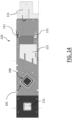
- the device may be a TCU 120.
- the TCU may comprise a plurality of different components 111 in addition to the PCB 102, the support component 101 and the antenna 100.
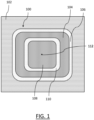
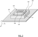
- FIG. 1 and FIG. 2 The GNSS antenna of the prior art is displayed in FIG. 1 and FIG. 2 and comprises an antenna 100 placed on a PCB 102.
- FIG. 3 to FIG. 6 display results of tests carried out on the GNSS antenna and PCB assembly of the prior art.
- FIG. 10 to FIG. 13 , FIG. 15 and FIG. 16 display results of tests carried out on the antenna 100, support component 101 and PCB 102 according to the present disclosure.
- the antenna for these tests was also a GNSS antenna.
- a GNSS antenna is a right hand circular polarised antenna.
- FIG. 3 to FIG. 6 , FIG. 10 to FIG. 13 , FIG. 15 and FIG. 16 each display results for two frequency bands of a GN L1 (1.58 GHz) and L5 (1.18 GHz) of the antenna.
- FIG. 3 , FIG. 4 , FIG. 10 , FIG. 11 and FIG. 15 each show results for L1.
- FIG. 5 , FIG. 6 , FIG. 12 , FIG. 13 and FIG. 16 each show results for L5.
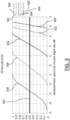
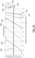
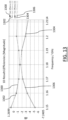
- FIG. 3 , FIG. 5 , FIG. 10 , FIG. 12 , FIG. 15 , and FIG. 16 shows 1D results for a cumulative distribution function for absolute realized gain.
- a representation is used to specify spherical coverage of an antenna.
- 0° is along the longitudinal axis (Z-direction) of the antenna 102.
- lines 301, 501, 1001, 1201, 1501, 1601 indicate the probability of gain being less than or equal to 0.5 (or 50%) for the antenna for each value in decibels.
- EIRP Equivalent isotropically radiated power
- FIG. 3 shows results for L1.
- the results are displayed by curves 300, 302, 304, 306, 308.
- Curve 300 represents results for signals radiating from 0° to 20°.
- Curve 302 represents results for signals radiating from 20° to 30°.
- Curve 304 represents results for signals radiating from 30° to 50°.
- Curve 306 represents results for signals radiating from 50° to 70°.
- Curve 308 represents results for signals radiating from 70° to 85°.
- FIG. 4 displays 1D results displaying the efficiency (magnitude) of the curves 300, 302, 304, 306, 308 of FIG. 3 .
- the graph displays values in decibels (dB) as a function of frequency (GHz).
- Curve 400 and curve 402 each represent radiance efficiency.
- Curve 400 represents ideal efficiency and curve 402 represents actual efficiency.
- curve 402 is superimposed on curve 400.
- Curve 404 and curve 406 each represent total efficiency.
- Curve 404 represents ideal efficiency and curve 406 represents actual efficiency.
- curve 404 is superimposed on curve 406.
- FIG. 5 shows results for L5.
- the results are displayed by curves 500, 502, 504, 506, 508.
- Curve 500 represents results for signals radiating from 0° to 20°.
- Curve 502 represents results for signals radiating from 20° to 30°.
- Curve 504 represents results for signals radiating from 30° to 50°.
- Curve 506 represents results for signals radiating from 50° to 70°.
- Curve 508 represents results for signals radiating from 70° to 85°.
- FIG. 6 displays 1D results displaying the efficiency (magnitude) of the curves 500, 502, 504, 506, 508 of FIG. 5 .
- the graph displays values in decibels (dB) as a function of frequency (GHz).
- Curve 600 and curve 602 each represent radiance efficiency.
- Curve 600 represents ideal efficiency and curve 602 represents actual efficiency.
- curve 602 is superimposed on curve 600.
- Curve 604 and curve 606 each represent total efficiency.
- Curve 604 represents ideal efficiency and curve 606 represents actual efficiency.
- curve 604 is superimposed on curve 606.
- FIG. 10 to FIG. 13 show results of tests carried out on the assembly alone.
- FIG. 15 and FIG. 16 show results of tests carried out on the assembly inside a TCU. As can be seen in each of these figures, the results are very close to the results without the support component.
- FIG. 10 shows results for L1.
- the results are displayed by curves 1000, 1002, 1004, 1006, 1008.
- Curve 1000 represents results for signals radiating from 0° to 20°.
- Curve 1002 represents results for signals radiating from 20° to 30°.
- Curve 1004 represents results for signals radiating from 30° to 50°.
- Curve 1006 represents results for signals radiating from 50° to 70°.
- Curve 1008 represents results for signals radiating from 70° to 85°.
- FIG. 11 displays 1D results displaying the efficiency (magnitude) of the curves 1000, 1002, 1004, 1006, 1008 of FIG. 10 .
- the graph displays values in decibels (dB) as a function of frequency (GHz).
- Curve 1100 and curve 1102 each represent radiance efficiency. Curve 1100 represents ideal efficiency and curve 1102 represents actual efficiency. As can be seen in FIG. 11 , curve 402 is superimposed on curve 1100.
- Curve 1104 and curve 1106 each represent total efficiency. Curve 1104 represents ideal efficiency and curve 1106 represents actual efficiency. As can be seen in FIG. 11 , curve 1104 is superimposed on curve 1106.
- FIG. 12 shows results for L5.
- the results are displayed by curves 1200, 1202, 1204, 1206, 1208.
- Curve 1200 represents results for signals radiating from 0° to 20°.
- Curve 1202 represents results for signals radiating from 20° to 30°.
- Curve 1204 represents results for signals radiating from 30° to 50°.
- Curve 1206 represents results for signals radiating from 50° to 70°.
- Curve 1208 represents results for signals radiating from 70° to 85°.
- FIG. 13 displays 1D results displaying the efficiency (magnitude) of the curves 1200, 1202, 1204, 1206, 1208 of FIG. 12 .
- the graph displays values in decibels (dB) as a function of frequency (GHz).
- Curve 1300 and curve 1302 each represent radiance efficiency.
- Curve 1300 represents ideal efficiency and curve 1302 represents actual efficiency.
- curve 1302 is superimposed on curve 1300.
- Curve 1304 and curve 1306 each represent total efficiency.
- Curve 1304 represents ideal efficiency and curve 1306 represents actual efficiency.
- curve 1304 is superimposed on curve 1306.
- FIG. 15 shows results for L1.
- the results are displayed by curves 1500, 1502, 1504, 1506, 1508.
- Curve 1500 represents results for signals radiating from 0° to 20°.
- Curve 1502 represents results for signals radiating from 20° to 30°.
- Curve 1504 represents results for signals radiating from 30° to 50°.
- Curve 1506 represents results for signals radiating from 50° to 70°.
- Curve 1508 represents results for signals radiating from 70° to 85°.
- FIG. 16 shows results for L5.
- the results are displayed by curves 1600, 1602, 1604, 1606, 1608.
- Curve 1600 represents results for signals radiating from 0° to 20°.
- Curve 1602 represents results for signals radiating from 20° to 30°.
- Curve 1604 represents results for signals radiating from 30° to 50°.
- Curve 1606 represents results for signals radiating from 50° to 70°.
- Curve 1608 represents results for signals radiating from 70° to 85°.
Landscapes
- Engineering & Computer Science (AREA)
- Remote Sensing (AREA)
- Physics & Mathematics (AREA)
- Electromagnetism (AREA)
- Support Of Aerials (AREA)
Abstract
It is provided a support component for an antenna on a PCB. The support component comprises a main surface area for receiving the antenna. The support component comprises a protruding portion extending from the main surface area and being fixedly connectable to the PCB so as to form a gap between the support component and the PCB. It is also provided a device comprising the PCB and the support component fixedly connected to the PCB and receiving the antenna.
Description
- The present invention relates to the field of antennae on PCBs, and more specifically to a support component for an antenna on a PCB. It is also provided a device comprising the support component, PCB and antenna.
- Telecom communications units (TCU) for vehicles are becoming more and more limited in space so as to satisfy vehicle design requirements. Electronic vehicle components for the TCU therefore need to become as small as possible to satisfy the vehicle manufacturer design requirements and fit the necessary amount of components within the TCU. For PCB's within the TCU, this involves designing the PCB layout to satisfy a space limitation, which is a complicated process, particularly for PCB's in communication with an antenna.
- Within this context, there is need for an improved support component for an antenna on a PCB.
- It is therefore provided a support component for an antenna on a PCB. The support component comprises a main surface for receiving the antenna. The support component comprises a protruding portion extending from the main surface and being fixedly connectable to the PCB so as to form a gap between the support component and the PCB.
- The support may comprise one or more of the following features:
- the support component is made of metal;
- the gap has a minimum distance of 2 mm;
- the gap has a maximum distance of 3 mm;
- the gap has a distance of 2 mm;
- the antenna is a GNSS antenna;
- the main surface has a minimum thickness of 0.3 mm;
- the main surface has a length ranging from 32 mm to 55 mm and a width ranging from 32 mm to 55 mm;
- the main surface has a length of 55 mm and a width of 55 mm;
- the protruding portion is fixedly connectable to the PCB by a glue or by soldering;
- the main surface is fixedly connectable to the antenna by a glue; and/or
- the main surface comprises a hole configured to receive one or more feed pins for connection to the PCB.
- It is also provided a device comprising a PCB and the support component fixedly connected to the PCB and receiving the antenna. The device may be a TCU.
- It is also provided a vehicle comprising the device.
- The support component makes it possible to address the need mentioned above. In particular, the support component provides an optimization of space as a result of the formed gap. Therefore, additional components for use on the PCB can be accounted for and used by placing them inside the gap. In other words, more space for PCB components is provided on the PCB by the gap and without increasing the dimensions and size of the PCB.
- This is achieved by the support component comprising a main surface and a protruding portion. The main surface is for receiving the antenna and ensures a stable bedding for the antenna. The main surface may substantially be a planar surface substantially parallel to the main planar surface of the PCB, i.e. the PCB face that comprises the PCB components. The protruding portion extends from the main surface so as to form a predetermined distance from the main surface. The protruding portion is also fixedly connectable to the PCB (e.g. fixedly connected) so that the predetermined distance formed by the protruding portion creates a gap between the PCB and the main surface. In other words, the protruding portion lies between the PCB and the main surface and creates a gap between them, so that the plane defined by the PCB and the plane defined by the main surface are parallel and at a predetermined non-negative distance. The antenna is consequently elevated from the PCB such that the additional components can be placed inside the gap. For example, additional components of the PCB may be placed inside the gap. In addition, the formation of the gap allows for providing additional space while ensuring use of an optimal quality antenna. In other words, additional space can be created without reducing the size of the antenna, which can result in a poorer quality of receiving signals.
- Advantageously and according to some embodiments, the support component may be made of metal. The support component may thereby act as both a support and a shield between the antenna and the PCB.
- Non-limiting examples will now be described in reference to the accompanying drawings, where:
-
FIG. 1 shows a plan view of an example of an antenna placed on a PCB, according to the prior art. -
FIG. 2 shows a perspective view of the example of an antenna placed on a PCB according to the prior art. -
FIG. 3 shows a graph of 1D results for a cumulative distribution function (CDF) of absolute realized gain, for L1 =1.58 GHz, according to prior art. -
FIG. 4 shows a graph of 1D results showing the efficiency [magnitude] of the results ofFIG. 3 . Values in decibels (dB) are displayed as a function of frequency (GHz). -
FIG. 5 shows a graph of 1D results for a cumulative distribution function (CDF) of absolute realized gain, for L5=1.18 GHz, according to prior art. -
FIG. 6 shows a graph of 1D results showing the efficiency [magnitude] of the results ofFIG. 5 . Values in decibels (dB) are displayed as a function of frequency (GHz). -
FIG. 7 shows a plan view of an example of an antenna placed on the support component, the support component of the present disclosure being placed on a PCB. -
FIG. 8 shows a perspective view of the example of an antenna placed on the support component, the support component of the present disclosure being placed on a PCB. -
FIG. 9 shows a perspective view of an example of the support of the present disclosure. -
FIG. 10 shows a graph of 1D results for a cumulative distribution function (CDF) of absolute realized gain, for L1=1.58 GHz. -
FIG. 11 shows a graph of 1D results showing the efficiency [magnitude] of the results ofFIG. 10 . Values in decibels (dB) are displayed as a function of frequency (GHz). -
FIG. 12 shows a graph of 1D results for a cumulative distribution function (CDF) of absolute realized gain, for L5=1.18 GHz. -
FIG. 13 shows a graph of 1D results showing the efficiency [magnitude] of the results ofFIG. 12 . Values in decibels (dB) are displayed as a function of frequency (GHz). -
FIG. 14 shows an example of the device of the present disclosure. -
FIG. 15 shows a graph of 1D results for a cumulative distribution function (CDF) of absolute realized gain, for L1=1.58 GHz, for tests carried out inside a TCU. -
FIG. 16 shows a graph of 1D results for a cumulative distribution function (CDF) of absolute realized gain, for L5=1.18 GHz, for tests carried out inside a TCU. - The disclosure will now be described in detail without limitation in the following description.
- It is provided a support component for an antenna on a PCB. The support component comprises a main surface for receiving the antenna. The support component comprises a protruding portion extending from the main surface and being fixedly connectable to the PCB so as to form a gap between the support and the PCB.
- It is also provided a device comprising the PCB and the support component fixedly connected to the PCB and receiving the antenna. The device may comprise any one or more of the features described herein.
- The support component is a component for holding up the antenna, i.e. for bearing the weight of the antenna. The support component may be a rigid structure. The support component may be particularly suitable for being installed inside a vehicle, such as a car. For example, the support component may be installed inside the dashboard of the car. Installing the support component in such an area can therefore provide for additional useable space inside the dashboard for other components, such as other components for placing upon the PCB. In fact, it is also provided a vehicle comprising the device.
- The antenna is the interface between radio waves propagating through space and electric currents moving in metal conductors, used with a transmitter or receiver. In transmission, a radio transmitter may supply an electric current to the terminals of the antenna, and the antenna may radiate the energy from the current as electromagnetic waves (radio waves). In reception, the antenna may intercept some of the power of a radio wave in order to produce an electric current at its terminals, that is applied to a receiver to be amplified.
- The PCB (printed circuit board) is a medium used to connect electronic components to one another in a controlled manner. It is in the form of a laminated sandwich structure of conductive and insulating layers: each of the conductive layers is designed with a pattern of traces, planes and/or other features, etched from one or more sheet layers of copper laminated onto and/or between sheet layers of a non-conductive substrate. Electrical components may be fixed to conductive pads on the outer layers in the shape designed to accept the component's terminals, generally by means of soldering, to both electrically connect and mechanically fasten them to it. Additionally or alternatively, connections may be made using vias (plated-through holes that allow interconnections between layers).
- The main surface for receiving the antenna is the surface of the support component that comes in physical contact with the antenna.
- The protruding portion extending from the main surface and being fixedly connectable to the PCB results in the protruding portion extending in a direction substantially orthogonal to that of the main surface receiving the PCB. In other words, the protruding portion extending from the main surface and being fixedly connectable to the PCB results in the protruding portion being orthogonal to the plane of the main surface.
- By the protruding portion being fixedly connectable to the PCB, once connected, the support component is fastened to the PCB in a secure position.
- The gap between the support component and the PCB is a pocket or space between each of these components.
- As shown in
FIG. 7 to FIG. 9 , anantenna 100 may be placed on thesupport component 101. Thesupport component 101 may be positioned on aPCB 102. Thesupport component 101 comprises amain surface 103. The main 103 surface may have a surface area that is greater than or equal to the surface area of the antenna received by thesupport component 101. Themain surface 103 may be a flat surface. Themain surface 103 may have the largest surface area of all the surfaces of thesupport component 101. Themain surface 103 may comprise a top side and a bottom side. The top side may receive the antenna (and therefore face the antenna) and the bottom side may face thePCB 102. - An shown in
FIG. 8 andFIG. 9 , the protrudingportion 105 extends from the main surface area and is fixedly connected to thePCB 102. Agap 107 is thereby formed between the support component and thePCB 102. The protrudingportion 105 may protrude uniformly, so that the protrudingportion 105 has a constant length. The top side may be the side opposite to the direction in which the protrudingportion 105 is protruding. - The protruding
portion 105 may be discontinuous. In other words, the protrudingportion 105 may comprise multiple sub-portions. The protrudingportion 105 may for example comprise two protruding sub-portions 105a, 105b. InFIG. 8 and9 , the protruding portion is for example made of two protruding sub-portions 105a, 105b which are walls in the z direction between themain surface 103 and thePCB 102. The protruding sub-portions 105a, 105b may protrude from opposite edges of the main surface, so as to form the two protruding sub-portions 105a, 105b. According to some examples, the protruding sub-portions may protrude from more than two opposing edges of themain surface 103. The examples shown inFIG.s 8-9 show the sub-portions 105a, 105b protruding from the edges which are opposite one another according to the direction x, but in alternative examples, the sub-portions 105a, 105b may protrude form the edges which are opposite one another according to direction y. Yet alternatively, the protrudingportion 105 may be formed by four walls each protruding from an edge of themain surface 103, the protrudingportion 105 thereby closing the gap. Yet alternatively, the protruding portions may not be walls as shown in the figures, but may be pods or pedestals, for example equally spaced and/or distributed, for example one at corner of themain surface 103. - Alternatively and according to some examples, the protruding
portion 105 may be continuous. That is to say, the protrudingportion 105 may comprise only one portion. The protruding portion may follow a predetermined length of the perimeter of themain surface 103. The predetermined length may be less than the perimeter of themain surface 103. Alternatively, the predetermined length may be equal to the perimeter of themain surface 103. - The
main surface 103 may have a square or rectangular shape (when viewed from a plan view). Alternatively themain surface 103 may have a shape other than a square or rectangular shape, for example a curved shape (when viewed from a plan view). - The protruding
portion 105 may comprise two sub-portions 105a, 105b opposite one another. - The protruding portion may be fixedly connectable to the
PCB 102 by a surface of the protruding portion that is parallel to the main surface (i.e. parallel to the plan of the main surface). - The support component may be made of metal. The support component can thereby act as a shield for protecting the antenna and
PCB 102 below. When connected to thePCB 102, the support component may thereby be grounded to thePCB 102. The support component may provide to thePCB 102 an electromagnetic shielding that blocks radio frequency (RF) electromagnetic radiation (also known as RF shielding) from the antenna. The metal may, for example, be any one of copper, brass, nickel, silver, steel (for example stainless steel), and tin. The metal may be selected depending on a preference for either reflecting electrically dominant waves, or for absorbing/suppressing magnetically dominant waves. - The
gap 107 formed between thePCB 102 and support component may have a predetermined distance. By distance it is meant the distance between the plane defined by the surface of thePCB 102 facing themain surface 103 and the plane defined by themain surface 103 facing thePCB 102. Thegap 107 may have a distance ranging from 1 mm to 4 mm. Thegap 107 may have a minimum distance of 2 mm, or for example, thegap 107 may have a minimum distance of 1.5 mm, or for example, a minimum distance of 1 mm. Thisgap 107 can therefore be large enough to allow for the placement of one or more components between thesupport component 101 andPCB 102, for which there would otherwise be no available space in an electrical component assembly (for example, in a vehicle, for example, in a TCU box in a vehicle). Thegap 107 may have a maximum distance of 3 mm, or for example a maximum distance of 3.5 mm, or for example a maximum distance of 4 mm. This can allow for one or more components to be placed within thegap 107 while also meeting design requirements for the overall height of the assembled device, the device being for example inside a TCU. Thegap 107 may have a distance of 2 mm, or of substantially 2 mm. This distance may allow for the incorporation of a network access device (NAD) between thesupport component 101 and thePCB 102. - The radio waves may be transmitted from a satellite. In such as case, the
antenna 100 may be a global navigation satellite system (GNSS) antenna (also referred to as a GNSS receiver). The GNSS receiver may receive a satellite signal transmitted from a GNSS satellite constellation through an antenna. The GNSS may operate at two frequency bands L1, L5. A microstrip patch antenna with a stacked structure and a single feed may be used for the purpose of dual-band operation. - The main surface may have a minimum thickness (i.e. in the z direction) of 0.3 mm, or for example, a minimum thickness of 0.35 mm, or for example a minimum thickness of 0.4 mm, or for example a minimum thickness of 0.45 mm, or for example a minimum thickness of 0.5 mm. This can allow the support component to adequately uphold the
antenna 100 so as to maintain thegap 107 between thesupport component 101 and thePCB 102. In addition, a minimum thickness of 0.3 mm can allow for maximizing the size of thegap 107 beneath. - As shown in
FIG. 7 andFIG. 8 , theantenna 100 may comprise two separate layers; atop surface layer 113 and abottom surface layer 115. Eachlayer ceramic part respective layer part ceramic parts main surface 103 may have dimensions such that the area of themain surface 103 is large enough to receive the antenna 100 (or the bottom surface layer 115). In other words, the area of themain surface 103 may be greater than or equal to the area of the surface of theantenna 100 that comes into contact with the main surface 103 (or the bottom surface layer 115). Theantenna 100 may (or at least the bottom surface layer 115) have a length of 32 mm and a width of 32 mm. Themain surface area 103 may have dimensions that are greater than or equal to the surface of theantenna 100 that comes into contact with the main surface 103 (or the bottom surface layer 115). Themain surface 103 may have a length ranging from 32 mm to 55 mm and a width ranging from 32 mm to 55 mm, for example, a length of 32 mm and a width of 32 mm, or for example, a length of 32 mm to 40 mm and a width of 32 mm to 40 mm, or for example a length of 40 mm to 45 mm and a width of 40 mm to 45 mm, or for example a length of 45 mm to 50 mm and a width of 45 mm to 50 mm, or for example a length of 50 mm to 55 mm and a width of 50 mm to 55 mm, or for example a length of 55 mm and a width of 55 mm. The length and width may be equal to one another. Alternatively, the length and width may different to one another. Having dimensions that are greater than those of theantenna 100 can allow for securely supporting theantenna 100 while also providing sufficient space in the area of the gap in the X and/or Y directions. Preferably, for a GNSS antenna, themain surface 103 may have a length of 55 mm and a width of 55 mm, allowing for secure support of theantenna 100 while providing sufficient space in the area of the gap in the X and Y directions. - The protruding
portion 105 may be fixedly connectable to thePCB 102 by a glue. This can facilitate an easy assembling of the device and can improve the rigidity of the connection between the protrudingportion 105 and thePCB 102. Alternatively, the protrudingportion 105 may be fixedly connectable to thePCB 102 by soldering. In addition to improving a rigid connection between the protrudingportion 105 and thePCB 102, this can allow for ensuring that theantenna 100 is grounded to thePCB 102 through thesupport component 101, if thesupport component 101 is made of metal. - The
main surface 103 may be fixedly connectable to theantenna 100 by a glue. This can facilitate an easy assembling of the device and can provide a rigid connection between themain surface 103 and theantenna 100. - As shown in
FIG. 9 , themain surface 103 may comprise ahole 109 configured to receive one or more feed pins (not shown in figures) for connection to the PCB. The one or more pins may connect a feed point 112 (seeFIG. 7 andFIG. 8 ) to thePCB 102 beneath. Thefeed point 112 may receive signals and transfer the signals to theconductive layers PCB 102 for transfer of the signals to thePCB 102. The pins may pass through thehole 109 and may be connected to thePCB 102. The pins may be soldered to thePCB 102. - The device of the present disclosure comprises the
PCB 102, thesupport component 101 and theantenna 100. As shown inFIG. 14 , the device may be aTCU 120. The TCU may comprise a plurality ofdifferent components 111 in addition to thePCB 102, thesupport component 101 and theantenna 100. - A number of tests were carried out to examine the performance of the
support component 101. The tests were compared to standard results of a GNSS antenna of the prior art without asupport component 101. The GNSS antenna of the prior art is displayed inFIG. 1 andFIG. 2 and comprises anantenna 100 placed on aPCB 102.FIG. 3 to FIG. 6 display results of tests carried out on the GNSS antenna and PCB assembly of the prior art. -
FIG. 10 to FIG. 13 ,FIG. 15 andFIG. 16 display results of tests carried out on theantenna 100,support component 101 andPCB 102 according to the present disclosure. The antenna for these tests was also a GNSS antenna. A GNSS antenna is a right hand circular polarised antenna. -
FIG. 3 to FIG. 6 ,FIG. 10 to FIG. 13 ,FIG. 15 andFIG. 16 each display results for two frequency bands of a GN L1 (1.58 GHz) and L5 (1.18 GHz) of the antenna.FIG. 3 ,FIG. 4 ,FIG. 10 ,FIG. 11 andFIG. 15 each show results for L1.FIG. 5 ,FIG. 6 ,FIG. 12 ,FIG. 13 andFIG. 16 each show results for L5. - Each of
FIG. 3 ,FIG. 5 ,FIG. 10 ,FIG. 12 ,FIG. 15 , andFIG. 16 shows 1D results for a cumulative distribution function for absolute realized gain. As it is known in the field of antennas, such a representation is used to specify spherical coverage of an antenna. For each ofFIG. 3 ,FIG. 5 ,FIG. 10 ,FIG. 12 ,FIG. 15 , andFIG. 16 , 0° is along the longitudinal axis (Z-direction) of theantenna 102. Each oflines - As previously mentioned,
FIG. 3 shows results for L1. The results are displayed bycurves Curve 300 represents results for signals radiating from 0° to 20°.Curve 302 represents results for signals radiating from 20° to 30°.Curve 304 represents results for signals radiating from 30° to 50°.Curve 306 represents results for signals radiating from 50° to 70°.Curve 308 represents results for signals radiating from 70° to 85°. -
FIG. 4 displays 1D results displaying the efficiency (magnitude) of thecurves FIG. 3 . The graph displays values in decibels (dB) as a function of frequency (GHz).Curve 400 andcurve 402 each represent radiance efficiency.Curve 400 represents ideal efficiency andcurve 402 represents actual efficiency. As can be seen inFIG. 4 ,curve 402 is superimposed oncurve 400.Curve 404 andcurve 406 each represent total efficiency.Curve 404 represents ideal efficiency andcurve 406 represents actual efficiency. As can be seen inFIG. 4 ,curve 404 is superimposed oncurve 406. - As previously mentioned,
FIG. 5 shows results for L5. The results are displayed bycurves Curve 500 represents results for signals radiating from 0° to 20°.Curve 502 represents results for signals radiating from 20° to 30°.Curve 504 represents results for signals radiating from 30° to 50°.Curve 506 represents results for signals radiating from 50° to 70°.Curve 508 represents results for signals radiating from 70° to 85°. -
FIG. 6 displays 1D results displaying the efficiency (magnitude) of thecurves FIG. 5 . The graph displays values in decibels (dB) as a function of frequency (GHz).Curve 600 andcurve 602 each represent radiance efficiency.Curve 600 represents ideal efficiency andcurve 602 represents actual efficiency. As can be seen inFIG. 6 ,curve 602 is superimposed oncurve 600.Curve 604 andcurve 606 each represent total efficiency.Curve 604 represents ideal efficiency andcurve 606 represents actual efficiency. As can be seen inFIG. 6 ,curve 604 is superimposed oncurve 606. -
FIG. 10 to FIG. 13 show results of tests carried out on the assembly alone.FIG. 15 andFIG. 16 show results of tests carried out on the assembly inside a TCU. As can be seen in each of these figures, the results are very close to the results without the support component. - As previously mentioned,
FIG. 10 shows results for L1. The results are displayed bycurves Curve 1000 represents results for signals radiating from 0° to 20°.Curve 1002 represents results for signals radiating from 20° to 30°.Curve 1004 represents results for signals radiating from 30° to 50°.Curve 1006 represents results for signals radiating from 50° to 70°.Curve 1008 represents results for signals radiating from 70° to 85°. -
FIG. 11 displays 1D results displaying the efficiency (magnitude) of thecurves FIG. 10 . The graph displays values in decibels (dB) as a function of frequency (GHz).Curve 1100 andcurve 1102 each represent radiance efficiency.Curve 1100 represents ideal efficiency andcurve 1102 represents actual efficiency. As can be seen inFIG. 11 ,curve 402 is superimposed oncurve 1100.Curve 1104 andcurve 1106 each represent total efficiency.Curve 1104 represents ideal efficiency andcurve 1106 represents actual efficiency. As can be seen inFIG. 11 ,curve 1104 is superimposed oncurve 1106. - As previously mentioned,
FIG. 12 shows results for L5. The results are displayed bycurves Curve 1200 represents results for signals radiating from 0° to 20°.Curve 1202 represents results for signals radiating from 20° to 30°.Curve 1204 represents results for signals radiating from 30° to 50°.Curve 1206 represents results for signals radiating from 50° to 70°.Curve 1208 represents results for signals radiating from 70° to 85°. -
FIG. 13 displays 1D results displaying the efficiency (magnitude) of thecurves FIG. 12 . The graph displays values in decibels (dB) as a function of frequency (GHz).Curve 1300 andcurve 1302 each represent radiance efficiency.Curve 1300 represents ideal efficiency andcurve 1302 represents actual efficiency. As can be seen inFIG. 13 ,curve 1302 is superimposed oncurve 1300.Curve 1304 andcurve 1306 each represent total efficiency.Curve 1304 represents ideal efficiency andcurve 1306 represents actual efficiency. As can be seen inFIG. 13 ,curve 1304 is superimposed oncurve 1306. - As previously mentioned,
FIG. 15 shows results for L1. The results are displayed bycurves Curve 1500 represents results for signals radiating from 0° to 20°.Curve 1502 represents results for signals radiating from 20° to 30°.Curve 1504 represents results for signals radiating from 30° to 50°.Curve 1506 represents results for signals radiating from 50° to 70°.Curve 1508 represents results for signals radiating from 70° to 85°. - As previously mentioned,
FIG. 16 shows results for L5. The results are displayed bycurves Curve 1600 represents results for signals radiating from 0° to 20°.Curve 1602 represents results for signals radiating from 20° to 30°.Curve 1604 represents results for signals radiating from 30° to 50°.Curve 1606 represents results for signals radiating from 50° to 70°.Curve 1608 represents results for signals radiating from 70° to 85°.
Claims (15)
- A support component for an antenna on a PCB, comprising:- a main surface for receiving the antenna;- a protruding portion extending from the main surface and being fixedly connectable to the PCB so as to form a gap between the support component and the PCB.
- The support component of claim 1, wherein the support component is made of metal.
- The support component of claim 1 or 2, wherein the gap has a minimum distance of 2 mm.
- The support component according to any one of claims 1 to 3, wherein the gap has a maximum distance of 3 mm.
- The support component according to any one of claims 1 to 4, wherein the gap has a distance of 2 mm.
- The support component according to any one of claims 1 to 5, wherein the antenna is a GNSS antenna.
- The support component according to any one of claims 1 to 6, wherein the main surface has a minimum thickness of 0.3 mm.
- The support component according to any one of claims 1 to 7, wherein the main surface has a length ranging from 32 mm to 55 mm and a width ranging from 32 mm to 55 mm.
- The support component according to any one of claims 1 to 8, wherein the main surface has a length of 55 mm and a width of 55 mm.
- The support component according to any one of claims 1 to 9, wherein the protruding portion is fixedly connectable to the PCB by a glue or by soldering.
- The support component according to any one of claims 1 to 10, wherein the main surface is fixedly connectable to the antenna by a glue.
- The support component according to any one of claims 1 to 11, wherein the main surface comprises a hole configured to receive one or more feed pins for connection to the PCB.
- A device comprising:- a PCB;- the support component of any one of claims 1 to 12 fixedly connected to the PCB and receiving the antenna.
- The device according to claim 13, wherein the device is a TCU.
- A vehicle comprising the device of claim 13 or 14.
Priority Applications (1)
| Application Number | Priority Date | Filing Date | Title |
|---|---|---|---|
| EP23193885.3A EP4518020A1 (en) | 2023-08-29 | 2023-08-29 | Support component for an antenna on a pcb |
Applications Claiming Priority (1)
| Application Number | Priority Date | Filing Date | Title |
|---|---|---|---|
| EP23193885.3A EP4518020A1 (en) | 2023-08-29 | 2023-08-29 | Support component for an antenna on a pcb |
Publications (1)
| Publication Number | Publication Date |
|---|---|
| EP4518020A1 true EP4518020A1 (en) | 2025-03-05 |
Family
ID=87863446
Family Applications (1)
| Application Number | Title | Priority Date | Filing Date |
|---|---|---|---|
| EP23193885.3A Withdrawn EP4518020A1 (en) | 2023-08-29 | 2023-08-29 | Support component for an antenna on a pcb |
Country Status (1)
| Country | Link |
|---|---|
| EP (1) | EP4518020A1 (en) |
Citations (4)
| Publication number | Priority date | Publication date | Assignee | Title |
|---|---|---|---|---|
| JP3185618B2 (en) * | 1995-07-28 | 2001-07-11 | 株式会社デンソー | Radio receiver |
| US20130120210A1 (en) * | 2011-11-14 | 2013-05-16 | Continental Automotive Systems, Inc. | Gps antenna on-shield/housing with grounding |
| WO2020153428A1 (en) * | 2019-01-25 | 2020-07-30 | 株式会社デンソー | Wireless communication device |
| CN116636088A (en) * | 2020-12-23 | 2023-08-22 | 株式会社友华 | Chip Antenna and Vehicle Antenna Device |
-
2023
- 2023-08-29 EP EP23193885.3A patent/EP4518020A1/en not_active Withdrawn
Patent Citations (4)
| Publication number | Priority date | Publication date | Assignee | Title |
|---|---|---|---|---|
| JP3185618B2 (en) * | 1995-07-28 | 2001-07-11 | 株式会社デンソー | Radio receiver |
| US20130120210A1 (en) * | 2011-11-14 | 2013-05-16 | Continental Automotive Systems, Inc. | Gps antenna on-shield/housing with grounding |
| WO2020153428A1 (en) * | 2019-01-25 | 2020-07-30 | 株式会社デンソー | Wireless communication device |
| CN116636088A (en) * | 2020-12-23 | 2023-08-22 | 株式会社友华 | Chip Antenna and Vehicle Antenna Device |
Similar Documents
| Publication | Publication Date | Title |
|---|---|---|
| CN110785893B (en) | Antenna module and communication device | |
| CN1316679C (en) | ELectronic appts. and printed circuit board for mounting antenna | |
| EP2538489B1 (en) | Composite resonating antenna structure | |
| EP3051628B1 (en) | Antenna apparatus and electronic device having same | |
| US6570538B2 (en) | Symmetrical antenna structure and a method for its manufacture as well as an expansion card applying the antenna structure | |
| US9048543B2 (en) | Orthogonal modular embedded antenna, with method of manufacture and kits therefor | |
| EP3935689B1 (en) | Antenna structure and method for manufacturing the same | |
| WO2020142171A1 (en) | System and method with multilayer laminated waveguide antenna | |
| EP3465823B1 (en) | C-fed antenna formed on multi-layer printed circuit board edge | |
| US7724192B2 (en) | Portable communication device with slot-coupled antenna module | |
| US20120206301A1 (en) | Multi-angle ultra wideband antenna with surface mount technology methods of assembly and kits therefor | |
| WO2001041257A1 (en) | Antenna device with transceiver circuitry | |
| US20070229367A1 (en) | Antenna apparatus | |
| EP1730810B1 (en) | High gain antenna for microwave frequencies | |
| US12249777B2 (en) | Ultra-wideband antenna device | |
| EP2681799A2 (en) | Multi-angle ultra wideband antenna with surface mount technology methods of assembly and kits therefor | |
| EP4518020A1 (en) | Support component for an antenna on a pcb | |
| EP4597744A1 (en) | Antenna assembly | |
| US8228235B2 (en) | High gain antenna for microwave frequencies | |
| CN220774736U (en) | Antenna structure and terminal equipment | |
| US20210013582A1 (en) | Radio frequency modules with millimeter-wave air-gap phased-array antenna | |
| EP4723370A1 (en) | Horizontally-polarized omnidirectional antenna with broadband amplitude taper | |
| US11778730B1 (en) | Printed circuit board and wireless communication terminal | |
| EP4546558A1 (en) | A gnss/sdars antenna system | |
| US12562473B2 (en) | LGA- and BGA-based phased-array millimeter-wave antennas |
Legal Events
| Date | Code | Title | Description |
|---|---|---|---|
| PUAI | Public reference made under article 153(3) epc to a published international application that has entered the european phase |
Free format text: ORIGINAL CODE: 0009012 |
|
| STAA | Information on the status of an ep patent application or granted ep patent |
Free format text: STATUS: THE APPLICATION HAS BEEN PUBLISHED |
|
| AK | Designated contracting states |
Kind code of ref document: A1 Designated state(s): AL AT BE BG CH CY CZ DE DK EE ES FI FR GB GR HR HU IE IS IT LI LT LU LV MC ME MK MT NL NO PL PT RO RS SE SI SK SM TR |
|
| STAA | Information on the status of an ep patent application or granted ep patent |
Free format text: STATUS: THE APPLICATION IS DEEMED TO BE WITHDRAWN |
|
| 18D | Application deemed to be withdrawn |
Effective date: 20250906 |