EP4518011A1 - Voltage detection device and battery module - Google Patents
Voltage detection device and battery module Download PDFInfo
- Publication number
- EP4518011A1 EP4518011A1 EP23795954.9A EP23795954A EP4518011A1 EP 4518011 A1 EP4518011 A1 EP 4518011A1 EP 23795954 A EP23795954 A EP 23795954A EP 4518011 A1 EP4518011 A1 EP 4518011A1
- Authority
- EP
- European Patent Office
- Prior art keywords
- voltage detection
- socket
- detection device
- holder
- plug
- Prior art date
- Legal status (The legal status is an assumption and is not a legal conclusion. Google has not performed a legal analysis and makes no representation as to the accuracy of the status listed.)
- Pending
Links
Images



Classifications
-
- H—ELECTRICITY
- H01—ELECTRIC ELEMENTS
- H01M—PROCESSES OR MEANS, e.g. BATTERIES, FOR THE DIRECT CONVERSION OF CHEMICAL ENERGY INTO ELECTRICAL ENERGY
- H01M10/00—Secondary cells; Manufacture thereof
- H01M10/42—Methods or arrangements for servicing or maintenance of secondary cells or secondary half-cells
- H01M10/48—Accumulators combined with arrangements for measuring, testing or indicating the condition of cells, e.g. the level or density of the electrolyte
- H01M10/482—Accumulators combined with arrangements for measuring, testing or indicating the condition of cells, e.g. the level or density of the electrolyte for several batteries or cells simultaneously or sequentially
-
- G—PHYSICS
- G01—MEASURING; TESTING
- G01R—MEASURING ELECTRIC VARIABLES; MEASURING MAGNETIC VARIABLES
- G01R31/00—Arrangements for testing electric properties; Arrangements for locating electric faults; Arrangements for electrical testing characterised by what is being tested not provided for elsewhere
- G01R31/36—Arrangements for testing, measuring or monitoring the electrical condition of accumulators or electric batteries, e.g. capacity or state of charge [SoC]
- G01R31/396—Acquisition or processing of data for testing or for monitoring individual cells or groups of cells within a battery
-
- G—PHYSICS
- G01—MEASURING; TESTING
- G01R—MEASURING ELECTRIC VARIABLES; MEASURING MAGNETIC VARIABLES
- G01R31/00—Arrangements for testing electric properties; Arrangements for locating electric faults; Arrangements for electrical testing characterised by what is being tested not provided for elsewhere
- G01R31/36—Arrangements for testing, measuring or monitoring the electrical condition of accumulators or electric batteries, e.g. capacity or state of charge [SoC]
-
- G—PHYSICS
- G01—MEASURING; TESTING
- G01R—MEASURING ELECTRIC VARIABLES; MEASURING MAGNETIC VARIABLES
- G01R31/00—Arrangements for testing electric properties; Arrangements for locating electric faults; Arrangements for electrical testing characterised by what is being tested not provided for elsewhere
- G01R31/36—Arrangements for testing, measuring or monitoring the electrical condition of accumulators or electric batteries, e.g. capacity or state of charge [SoC]
- G01R31/382—Arrangements for monitoring battery or accumulator variables, e.g. SoC
- G01R31/3835—Arrangements for monitoring battery or accumulator variables, e.g. SoC involving only voltage measurements
-
- H—ELECTRICITY
- H01—ELECTRIC ELEMENTS
- H01M—PROCESSES OR MEANS, e.g. BATTERIES, FOR THE DIRECT CONVERSION OF CHEMICAL ENERGY INTO ELECTRICAL ENERGY
- H01M10/00—Secondary cells; Manufacture thereof
- H01M10/42—Methods or arrangements for servicing or maintenance of secondary cells or secondary half-cells
- H01M10/425—Structural combination with electronic components, e.g. electronic circuits integrated to the outside of the casing
-
- H—ELECTRICITY
- H01—ELECTRIC ELEMENTS
- H01M—PROCESSES OR MEANS, e.g. BATTERIES, FOR THE DIRECT CONVERSION OF CHEMICAL ENERGY INTO ELECTRICAL ENERGY
- H01M10/00—Secondary cells; Manufacture thereof
- H01M10/42—Methods or arrangements for servicing or maintenance of secondary cells or secondary half-cells
- H01M10/48—Accumulators combined with arrangements for measuring, testing or indicating the condition of cells, e.g. the level or density of the electrolyte
-
- H—ELECTRICITY
- H01—ELECTRIC ELEMENTS
- H01M—PROCESSES OR MEANS, e.g. BATTERIES, FOR THE DIRECT CONVERSION OF CHEMICAL ENERGY INTO ELECTRICAL ENERGY
- H01M50/00—Constructional details or processes of manufacture of the non-active parts of electrochemical cells other than fuel cells, e.g. hybrid cells
- H01M50/20—Mountings; Secondary casings or frames; Racks, modules or packs; Suspension devices; Shock absorbers; Transport or carrying devices; Holders
- H01M50/204—Racks, modules or packs for multiple batteries or multiple cells
- H01M50/207—Racks, modules or packs for multiple batteries or multiple cells characterised by their shape
- H01M50/209—Racks, modules or packs for multiple batteries or multiple cells characterised by their shape adapted for prismatic or rectangular cells
-
- H—ELECTRICITY
- H01—ELECTRIC ELEMENTS
- H01M—PROCESSES OR MEANS, e.g. BATTERIES, FOR THE DIRECT CONVERSION OF CHEMICAL ENERGY INTO ELECTRICAL ENERGY
- H01M50/00—Constructional details or processes of manufacture of the non-active parts of electrochemical cells other than fuel cells, e.g. hybrid cells
- H01M50/50—Current conducting connections for cells or batteries
- H01M50/502—Interconnectors for connecting terminals of adjacent batteries; Interconnectors for connecting cells outside a battery casing
- H01M50/519—Interconnectors for connecting terminals of adjacent batteries; Interconnectors for connecting cells outside a battery casing comprising printed circuit boards [PCB]
-
- H—ELECTRICITY
- H01—ELECTRIC ELEMENTS
- H01M—PROCESSES OR MEANS, e.g. BATTERIES, FOR THE DIRECT CONVERSION OF CHEMICAL ENERGY INTO ELECTRICAL ENERGY
- H01M50/00—Constructional details or processes of manufacture of the non-active parts of electrochemical cells other than fuel cells, e.g. hybrid cells
- H01M50/50—Current conducting connections for cells or batteries
- H01M50/569—Constructional details of current conducting connections for detecting conditions inside cells or batteries, e.g. details of voltage sensing terminals
-
- Y—GENERAL TAGGING OF NEW TECHNOLOGICAL DEVELOPMENTS; GENERAL TAGGING OF CROSS-SECTIONAL TECHNOLOGIES SPANNING OVER SEVERAL SECTIONS OF THE IPC; TECHNICAL SUBJECTS COVERED BY FORMER USPC CROSS-REFERENCE ART COLLECTIONS [XRACs] AND DIGESTS
- Y02—TECHNOLOGIES OR APPLICATIONS FOR MITIGATION OR ADAPTATION AGAINST CLIMATE CHANGE
- Y02E—REDUCTION OF GREENHOUSE GAS [GHG] EMISSIONS, RELATED TO ENERGY GENERATION, TRANSMISSION OR DISTRIBUTION
- Y02E60/00—Enabling technologies; Technologies with a potential or indirect contribution to GHG emissions mitigation
- Y02E60/10—Energy storage using batteries
Definitions
- the present invention relates to a voltage detection device and a battery module.
- a battery module includes a plurality of battery cells, a housing, a wire harness, and a connector.
- the housing accommodates the plurality of battery cells.
- the connector is electrically connected to the plurality of battery cells via the wire harness.
- the connector is attached to the housing.
- Patent Document 1 Japanese Patent Application Publication (Translation of PCT Application) No. 2020-517051
- One example of an object of the present invention is to improve workability for assembling a battery module. Another object of the present invention will be clarified from description of the present specification.
- One aspect of the present invention is as follows.
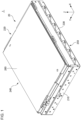
- Fig. 1 is a front perspective view of a battery module 1 according to an embodiment.
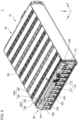
- Fig. 2 is a diagram with accommodation body 20 removed from Fig. 1 .
- the X direction indicates a front-rear direction of the battery module 1.
- a tip end side of the arrow indicating the X direction is a rear side of the battery module 1.
- a proximal end side of the arrow indicating the X direction is a front side of the battery module 1.
- the Y direction is orthogonal to the X direction.
- the Y direction indicates a left-right direction of the battery module 1.
- a tip end side of the arrow indicating the Y direction is a left side of the battery module 1.
- a proximal end side of the arrow indicating the Y direction is a right side of the battery module 1.
- the Z direction is orthogonal to both of the X direction and the Y direction.
- the Z direction indicates an up-down direction of the battery module 1.
- a tip end side of the arrow indicating the Z direction is an upper side of the battery module 1.
- a proximal end side of the arrow indicating the Z direction is a lower side of the battery module 1.
- the battery module 1 includes a cell stack 10, the accommodation body 20, a front voltage detection device 30, and a rear voltage detection device 30'.
- the cell stack 10 includes a plurality of cell groups 100G. Each cell group 100G includes a plurality of battery cells 100.
- the accommodation body 20 includes a front cover 210, a rear cover 220, a right cover 230, a left cover 240, a lower cover 250, and an upper cover 260.
- the front voltage detection device 30 includes a holder 310, a plurality of voltage detection lines 320, two sockets 330, and a terminal 340.
- a plurality of voltage detection tip end portions 322 are provided at ends of the plurality of voltage detection lines 320 on a side of a tab group 110 described later.
- the plurality of battery cells 100 are stacked in the Y direction.
- Each battery cell 100 has a substantially rectangular shape when viewed from the Y direction.
- a long direction of each battery cell 100 is substantially in parallel to the X direction.
- a short direction of each battery cell 100 is substantially in parallel to the Z direction.
- a thickness direction of each battery cell 100 is substantially in parallel to the Y direction.
- the structure of each battery cell 100 is not limited to this example.
- Each battery cell 100 includes an unillustrated battery element, an exterior member 102, a positive electrode tab 112, and a negative electrode tab 114.
- the exterior member 102 seals the battery element and unillustrated electrolytic liquid.
- the battery element includes a plurality of unillustrated positive electrodes and a plurality of unillustrated negative electrodes alternately stacked in the Y direction and an unillustrated separator located between the positive electrode and the negative electrode adjacent to each other in the Y direction.
- the positive electrode tab 112 and the negative electrode tab 114 are drawn out from opposite sides the exterior member 102 in the X direction.
- the positive electrode tab 112 is electrically connected to the above plurality of positive electrodes.
- the positive electrode tab 112 is composed of, for example, aluminum.
- the negative electrode tab 114 is electrically connected to the above plurality of negative electrodes.
- the negative electrode tab 114 is composed of, for example, copper.
- Each cell group 100G includes two battery cells 100 connected in parallel to each other.
- the positive electrode tabs 112 drawn out from two battery cells 100 included in each cell group 100G face the same side in the X direction.
- the negative electrode tabs 114 drawn out from two battery cells 100 included in each cell group 100G face the same side in the X direction.
- the positive electrode tabs 112 and the negative electrode tabs 114 drawn out from one of the cell groups 100G adjacent to each other in the Y direction and the positive electrode tabs 112 and the negative electrode tabs 114 drawn from the other of the cell groups 100G adjacent to each other in the Y direction face opposite sides in the X direction.
- the plurality of cell groups 100G are connected in series.
- the cell groups 100G adjacent to each other in the Y direction include a tab group 110 located on the front side or the rear side of the cell groups 100G.
- the tab group 110 includes the two positive electrode tabs 112 drawn from one of the cell groups 100G adjacent to each other in the Y direction and the two negative electrode tabs 114 drawn out from the other of the cell groups 100G adjacent to each other in the Y direction.
- the two positive electrode tabs 112 and the two negative electrode tabs 114 are joined to one another, for example, by laser welding.
- a plurality of tab groups 110 located on the front side of the cell stack 10 and a plurality of tab groups 110 located on the rear side of the cell stack 10 are alternately placed in the Y direction.
- the cell group 100G located on a leftmost side and the cell group 100G located second from the left side for example, include the tab group 110 located on the front side of these cell groups 100G.
- the cell group 100G located second from the left side and the cell group 100G located third from the left side include the tab group 110 located on the rear side of these cell groups 100G.
- each cell group 100G may include three or more battery cells 100.
- a plurality of single battery cells 100 may be connected in series.
- the accommodation body 20 includes the cell stack 10, the front voltage detection device 30, and the rear voltage detection device 30'.
- the front cover 210 covers the front side of the cell stack 10 and the front voltage detection device 30.
- the rear cover 220 covers the rear side of the cell stack 10 and the rear voltage detection device 30'.
- the right cover 230 covers a right side of the cell stack 10.
- the left cover 240 covers a left side of the cell stack 10.
- the lower cover 250 covers a lower side of the cell stack 10.
- the upper cover 260 covers an upper side of the cell stack 10.
- the holder 310 is provided on the front side of the cell stack 10.
- the holder 310 is formed of, for example, resin.
- the holder 310 integrally holds the plurality of voltage detection lines 320, the plurality of voltage detection tip end portions 322, and the two sockets 330. Therefore, positioning the holder 310 with respect to the cell stack 10 enables to position the plurality of voltage detection lines 320 and the plurality of voltage detection tip end portions 322.
- the holder 310 is positioned with respect to the cell stack 10 by attaching the holder 310 to the accommodation body 20.
- each of the plurality of voltage detection tip end portions 322 is located on the front side of each of the plurality of tab groups 110 located on the front side of the cell stack 10.
- the plurality of voltage detection lines 320 are, for example, a wire harness. Each of the plurality of voltage detection lines 320 electrically connects each of the plurality of tab groups 110 and the socket 330 to each other. Specifically, one end of each of the plurality of voltage detection lines 320 is electrically connected to each of the plurality of tab groups 110 located on the front side of the cell stack 10 via each of the plurality of voltage detection tip end potions 322. Each voltage detection tip end portion 322 is, for example, a conductive plate such as a metal plate. Each voltage detection tip end portion 322 is joined to a front surface of each tab group 110, for example, by laser welding. The other end of each of the plurality of voltage detection lines 320 is electrically connected to the socket 330.
- the terminal 340 is electrically connected to the positive electrode tab 112 drawn out to the front side from the battery cell 100 disposed on the rightmost side.
- the cell stack 10 is electrically connectable to external equipment via the terminal 340.
- the rear voltage detection device 30' includes an unillustrated holder, a plurality of unillustrated voltage detection lines, an unillustrated connector, and an unillustrated terminal.
- the terminal of the rear voltage detection device 30' is electrically connected to the negative electrode tab 114 drawn out to the rear side from the battery cell 100 disposed on the leftmost side.
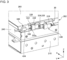
- Fig. 3 is an enlarged perspective view of one portion of the front voltage detection device 30 according to the embodiment.
- Fig. 4 is a diagram with the two sockets 330 and a plug 430 removed from Fig. 3 .
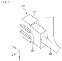
- Fig. 5 is a rear perspective view of the socket 330 according to the embodiment.
- the two sockets 330 and the plug 430 are described with reference to Fig. 3 .
- a step 262 is provided on a front end of the upper cover 260.
- the step 262 makes the front end portion of the upper cover 260 located at the position lower in the Z direction than the rear portion of the front end portion of the upper cover 260.
- the two sockets 330 illustrated in Fig. 3 are disposed in a space formed by the step 262. This can improve volumetric efficiency of the battery module 1.
- the plug 430 illustrated in Fig. 3 is connectable to the left socket 330 illustrated in Fig. 3 .
- the plug 430 includes a plurality of unillustrated terminals and a plug cover 434.
- the plurality of terminals of the plug 430 protrude toward the right side.
- the plug cover 434 surrounds the plurality of terminals of the plug 430 when viewed from a right side of the plug 430. Accordingly, foreign matter such as a finger of a worker or dust can be less likely to contact with the plurality of terminals of the plug 430 as compared with when the plurality of terminals of the plug 430 are not surrounded by the plug cover 434.
- the left socket 330 illustrated in Fig. 3 includes a body 332 and a socket cover 334. Some voltage detection lines 320 of the plurality of voltage detection lines 320 are electrically connected to the left socket 330 illustrated in Fig. 3 . In an example illustrated in Fig. 3 , the some the voltage detection lines 320 are connected to the socket 330 through a tube 324 attached to the socket 330.
- a plurality of terminal holes 332a is formed in the body 332.
- a terminal is embedded inside the plurality of terminal holes 332a.
- the terminal can be less likely to contact with foreign matter such as a finger of a worker or dust as compared with when the terminal of the socket 330 protrudes to outside.
- Each of the above plurality of terminals of the plug 430 is inserted through each of the plurality of terminal holes 332a in the Y direction.
- the socket 330 and the plug 430 are electrically connected to each other by inserting the plurality of terminals of the plug 430 through each of the plurality of terminal holes 332a in the Y direction.
- the socket cover 334 surrounds at least a portion of the body 332 with a gap 336 between them.
- the socket 330 and the plug 430 are connected to each other by inserting at least a portion of the plug cover 434 through the gap 336 in the Y direction. Accordingly, the mechanical connection of the socket 330 and the plug 430 can be strengthened as compared with when the gap 336 and the plug cover 434 are not provided.
- the gap 336 and the plug cover 434 may not be provided.
- the socket 330 and the plug 430 can be mechanically connected to each other by inserting each of the above plurality of terminals of the plug 430 through each of the plurality of terminal holes 332a in the Y direction.
- the right socket 330 illustrated in Fig. 3 includes a configuration similar to that of the left socket 330 illustrated in Fig. 3 .
- some of the voltage detection lines 320 can be electrically connected to one of the sockets 330 and the other of the voltage detection lines 320 can be electrically connected to the other socket 330.
- the number of terminal holes 332 of each socket 330 can be reduced as compared with when all the plurality of voltage detection lines 320 are electrically connected to a single socket 330.
- a width of each socket 330 in the Z direction can be reduced. This can prevent an upper surface of each socket 330 from protruding upward from an upper surface of the upper cover 260.
- the front voltage detection device 30 may include only one socket 330 or may include three or more sockets 330.
- the right socket 330 illustrated in Fig. 3 is disposed on the front side with respect to the left socket 330 illustrated in Fig. 3 . That is, the two sockets 330 illustrated in Fig. 3 are displaced from each other in the X direction. Accordingly, a space for passing the plurality of voltage detection lines 320 connected to the right socket 330 illustrated in Fig. 3 can be secured on the rear side of the left socket 330 illustrated in Fig. 3 . Accordingly, a space in the Y direction for arranging the two sockets 330 illustrated in Fig. 3 can be reduced as compared with when the two sockets 330 illustrated in Fig. 3 are aligned in the X direction.
- the layout of the sockets 330 is not limited to this example. For example, the two sockets 330 illustrated in Fig. 3 may be aligned in the X direction.
- a method of attaching the left socket 330 illustrated in Fig. 3 to the holder 310 is described by using Figs. 4 and 5 .
- a pair of locking grooves 352 are formed on a front surface of the holder 310.
- the pair of locking grooves 352 extend substantially in parallel to each other in the Y direction.
- a pair of locking portions 354 are provided on a rear surface of the socket cover 334.
- the pair of locking portions 354 extend substantially in parallel to the Y direction.
- the pair of locking portions 354 are insertable through the pair of locking grooves 352 from a left side of the pair of locking grooves 352 in the Y direction.
- the socket 330 is attached to the holder 310 by inserting the pair of locking portions 354 through the pair of locking grooves 352 from a left side of the pair of locking grooves 352 in the Y direction.
- the socket 330 is provided on the holder 310. Accordingly, the cell stack 10 and the front voltage detection device 30 can be accommodated in the accommodation body 20 after the front voltage detection device 30 is attached to the cell stack 10.
- the socket 330 is provided on the accommodation body 20 after the cell stack 10 is accommodated in the accommodation body 20.
- This case requires an extra length of the plurality of voltage detection lines 320 for drawing out the plurality of voltage detection lines 320 to the outside of the accommodation body 20.
- the embodiment does not need consideration of the extra length of the plurality of voltage detection lines 320.
- the workability for assembling the battery module 1 can be therefore improved as compared with when the socket 330 is provided on the accommodation body 20.
- Fig. 6 is an enlarged perspective view of a front portion of a front voltage detection device 30A according to a variant 1.
- the front voltage detection device 30A according to the variant 1 is similar to the front voltage detection device 30 according to the embodiment except for the following point.
- a socket 330A is embedded in a recess portion 312A formed on an upper surface of a holder 310A.
- a gap 336A is provided between an outer lateral surface of the socket 330A and an inner lateral surface of the recess portion 312A.
- a plug 430A is connectable to the socket 330A from an upper side of the socket 330A.
- the socket 330A and the plug 430A are mechanically connected to each other by inserting a plug cover 434A through the gap 336A in the Z direction. Also in the variant 1, the mechanical connection of the socket 330A and the plug 430A can be therefore strengthened similarly to the embodiment.
- Fig. 7 is an enlarged perspective view of a front portion of a front voltage detection device 30B according to a variant 2.
- the front voltage detection device 30B according to the variant 2 is similar to the front voltage detection device 30 according to the embodiment except for the following point.
- a socket 330B is embedded in a recess portion 312B formed on a front surface of a holder 310B.
- a gap 336B is provided between an outer lateral surface of the socket 330B and an inner lateral surface of the recess portion 312B.
- a plug 430B is connectable to the socket 330B from the front side of the socket 330B.
- the socket 330B and the plug 430B are mechanically connected to each other by inserting a plug cover 434B through the gap 336B in the X direction. Also in the variant 2, the mechanical connection of the socket 330B and the plug 430B can be therefore strengthened similarly to the embodiment.
- Fig. 8 is an enlarged perspective view of one portion of a front voltage detection device 30C according to a variant 3.
- the front voltage detection device 30C according to the variant 3 is similar to the front voltage detection device 30 according to the embodiment except for the following point.
- the front voltage detection device 30C includes a socket holder 350C.
- the socket holder 350C is attached to an unillustrated holder 310.
- the socket holder 350C holds a socket 330C.
- a plurality of terminal holes 332aC is provided on a left lateral surface of the socket 330C.
- the socket holder 350C holds the socket 330C with a gap 336C formed between the socket 330C and a portion of the socket holder 350C surrounding the socket 330C.
- the socket 330C and an unillustrated plug 430 are mechanically connected to each other by inserting an unillustrated plug cover 434 through the gap 336C in the Y direction similarly to the embodiment.
Landscapes
- Chemical & Material Sciences (AREA)
- Chemical Kinetics & Catalysis (AREA)
- Electrochemistry (AREA)
- General Chemical & Material Sciences (AREA)
- Physics & Mathematics (AREA)
- General Physics & Mathematics (AREA)
- Engineering & Computer Science (AREA)
- Manufacturing & Machinery (AREA)
- Microelectronics & Electronic Packaging (AREA)
- Battery Mounting, Suspending (AREA)
- Connection Of Batteries Or Terminals (AREA)
- Connector Housings Or Holding Contact Members (AREA)
- Secondary Cells (AREA)
- Measurement Of Current Or Voltage (AREA)
Abstract
Description
- The present invention relates to a voltage detection device and a battery module.
- For example, as described in
Patent Document 1, a battery module includes a plurality of battery cells, a housing, a wire harness, and a connector. The housing accommodates the plurality of battery cells. The connector is electrically connected to the plurality of battery cells via the wire harness. In a voltage detection device described inPatent Document 1, the connector is attached to the housing. - Patent Document 1:
Japanese Patent Application Publication (Translation of PCT Application) No. 2020-517051 - For example, as described in
Patent Document 1, when a connector is attached to a housing, the connector is attached to an accommodation body after a plurality of battery cells and a wire harness are accommodated in the housing. In this case, however, for example, the necessity of an extra length of a wire harness for drawing out the wire harness to an outside of a housing may cause reducing workability for assembling a battery module. - One example of an object of the present invention is to improve workability for assembling a battery module. Another object of the present invention will be clarified from description of the present specification.
- One aspect of the present invention is as follows.
- [1] A voltage detection device including:
- a holder;
- a plurality of voltage detection lines electrically connected to a plurality of battery cells and held on the holder; and
- a connector electrically connected to the plurality of voltage detection lines and provided on the holder.
- [2] The voltage detection device according to [1], in which the connector is provided with a terminal hole through which at least a portion of an external terminal is inserted.
- [3] The voltage detection device according to [1] or [2], in which there is a gap through which at least a portion of an external connector to be connected to the connector is inserted.
- [4] The voltage detection device according to any one of [1] to [3], further including attaching structure attaching the holder and the connector to each other.
- [5] A voltage detection device including:
- a holder;
- a plurality of voltage detection lines electrically connected to a plurality of battery cells and held on the holder; and
- a socket electrically connected to the plurality of voltage detection lines, in which
- at least a portion of the socket is embedded in a recess portion provided in the holder.
- [6] The voltage detection device according to [5], in which
there is a gap between the socket and the recess portion. - [7] The voltage detection device according to [5] or [6], in which
- the plurality of battery cells is stacked in a predetermined first direction,
- the holder is located on a side of a second direction orthogonal to the first direction with respect to the plurality of battery cells, and
- the recess portion is provided on a surface of the holder on a side of a third direction orthogonal to the first direction and the second direction.
- [8] A battery module including:
- the plurality of battery cells; and
- the voltage detection device according to any one of [1] to [7].
- Workability for assembling a battery module can be improved according to the above aspect of the present invention.
-
- [
Fig. 1 ] A front perspective view of a battery module according to an embodiment. - [
Fig. 2 ] A diagram with an accommodation body removed fromFig. 1 . - [
Fig. 3 ] An enlarged perspective view of one portion of a front voltage detection device according to the embodiment. - [
Fig. 4 ] A diagram with two sockets and a plug removed fromFig. 3 . - [
Fig. 5 ] A rear perspective view of the socket according to the embodiment. - [
Fig. 6 ] An enlarged perspective view of a front portion of a front voltage detection device according to avariant 1. - [
Fig. 7 ] An enlarged perspective view of a front portion of a front voltage detection device according to a variant 2. - [
Fig. 8 ] An enlarged perspective view of one portion of a front voltage detection device according to a variant 3. - Hereinafter, an embodiment according to the present invention is described by using the drawings. In all drawings, a similar constituent element is indicated by a similar reference sign, and description thereof is omitted as necessary.
-
Fig. 1 is a front perspective view of abattery module 1 according to an embodiment.Fig. 2 is a diagram withaccommodation body 20 removed fromFig. 1 . - In each drawing, an arrow indicating an X direction, a Y direction, and a Z direction is illustrated for explanation. The X direction indicates a front-rear direction of the
battery module 1. Hereinafter, unless otherwise specifically noted, a tip end side of the arrow indicating the X direction is a rear side of thebattery module 1. Hereinafter, unless otherwise specifically noted, a proximal end side of the arrow indicating the X direction is a front side of thebattery module 1. The Y direction is orthogonal to the X direction. The Y direction indicates a left-right direction of thebattery module 1. Hereinafter, unless otherwise specifically noted, a tip end side of the arrow indicating the Y direction is a left side of thebattery module 1.
Hereinafter, unless otherwise specifically noted, a proximal end side of the arrow indicating the Y direction is a right side of thebattery module 1. The Z direction is orthogonal to both of the X direction and the Y direction. The Z direction indicates an up-down direction of thebattery module 1. Hereinafter, unless otherwise specifically noted, a tip end side of the arrow indicating the Z direction is an upper side of thebattery module 1. Hereinafter, unless otherwise specifically noted, a proximal end side of the arrow indicating the Z direction is a lower side of thebattery module 1. The relations between the X direction, the Y direction, and the Z direction, and the front-rear direction, the left-right direction, and the up-down direction of thebattery module 1, however, is not limited to the above example. These relations differ according to an actual arrangement of thebattery module 1. - The
battery module 1 includes acell stack 10, theaccommodation body 20, a frontvoltage detection device 30, and a rear voltage detection device 30'. Thecell stack 10 includes a plurality ofcell groups 100G. Eachcell group 100G includes a plurality ofbattery cells 100. Theaccommodation body 20 includes afront cover 210, arear cover 220, aright cover 230, aleft cover 240, alower cover 250, and anupper cover 260. The frontvoltage detection device 30 includes aholder 310, a plurality ofvoltage detection lines 320, twosockets 330, and a terminal 340. A plurality of voltage detectiontip end portions 322 are provided at ends of the plurality ofvoltage detection lines 320 on a side of atab group 110 described later. - The plurality of
battery cells 100 are stacked in the Y direction. Eachbattery cell 100 has a substantially rectangular shape when viewed from the Y direction. A long direction of eachbattery cell 100 is substantially in parallel to the X direction. A short direction of eachbattery cell 100 is substantially in parallel to the Z direction. A thickness direction of eachbattery cell 100 is substantially in parallel to the Y direction. The structure of eachbattery cell 100, however, is not limited to this example. - Each
battery cell 100 includes an unillustrated battery element, anexterior member 102, apositive electrode tab 112, and anegative electrode tab 114. Theexterior member 102 seals the battery element and unillustrated electrolytic liquid. The battery element includes a plurality of unillustrated positive electrodes and a plurality of unillustrated negative electrodes alternately stacked in the Y direction and an unillustrated separator located between the positive electrode and the negative electrode adjacent to each other in the Y direction. Thepositive electrode tab 112 and thenegative electrode tab 114 are drawn out from opposite sides theexterior member 102 in the X direction. Thepositive electrode tab 112 is electrically connected to the above plurality of positive electrodes. Thepositive electrode tab 112 is composed of, for example, aluminum. Thenegative electrode tab 114 is electrically connected to the above plurality of negative electrodes. Thenegative electrode tab 114 is composed of, for example, copper. - Each
cell group 100G includes twobattery cells 100 connected in parallel to each other. Thepositive electrode tabs 112 drawn out from twobattery cells 100 included in eachcell group 100G face the same side in the X direction. Thenegative electrode tabs 114 drawn out from twobattery cells 100 included in eachcell group 100G face the same side in the X direction. Thepositive electrode tabs 112 and thenegative electrode tabs 114 drawn out from one of thecell groups 100G adjacent to each other in the Y direction and thepositive electrode tabs 112 and thenegative electrode tabs 114 drawn from the other of thecell groups 100G adjacent to each other in the Y direction face opposite sides in the X direction. - The plurality of
cell groups 100G are connected in series. Thecell groups 100G adjacent to each other in the Y direction include atab group 110 located on the front side or the rear side of thecell groups 100G. Thetab group 110 includes the twopositive electrode tabs 112 drawn from one of thecell groups 100G adjacent to each other in the Y direction and the twonegative electrode tabs 114 drawn out from the other of thecell groups 100G adjacent to each other in the Y direction. In thetab group 110, the twopositive electrode tabs 112 and the twonegative electrode tabs 114 are joined to one another, for example, by laser welding. A plurality oftab groups 110 located on the front side of thecell stack 10 and a plurality oftab groups 110 located on the rear side of thecell stack 10 are alternately placed in the Y direction. In an example illustrated inFig. 2 , therefore, thecell group 100G located on a leftmost side and thecell group 100G located second from the left side, for example, include thetab group 110 located on the front side of thesecell groups 100G. Thecell group 100G located second from the left side and thecell group 100G located third from the left side include thetab group 110 located on the rear side of thesecell groups 100G. - The structure of the
cell stack 10 is not limited to the above example. For example, eachcell group 100G may include three ormore battery cells 100. A plurality ofsingle battery cells 100 may be connected in series. - The
accommodation body 20 includes thecell stack 10, the frontvoltage detection device 30, and the rear voltage detection device 30'. Thefront cover 210 covers the front side of thecell stack 10 and the frontvoltage detection device 30. Therear cover 220 covers the rear side of thecell stack 10 and the rear voltage detection device 30'. Theright cover 230 covers a right side of thecell stack 10. Theleft cover 240 covers a left side of thecell stack 10. Thelower cover 250 covers a lower side of thecell stack 10. Theupper cover 260 covers an upper side of thecell stack 10. - The
holder 310 is provided on the front side of thecell stack 10. Theholder 310 is formed of, for example, resin. Theholder 310 integrally holds the plurality ofvoltage detection lines 320, the plurality of voltage detectiontip end portions 322, and the twosockets 330. Therefore, positioning theholder 310 with respect to thecell stack 10 enables to position the plurality ofvoltage detection lines 320 and the plurality of voltage detectiontip end portions 322. For example, theholder 310 is positioned with respect to thecell stack 10 by attaching theholder 310 to theaccommodation body 20. When theholder 310 is positioned, each of the plurality of voltage detectiontip end portions 322 is located on the front side of each of the plurality oftab groups 110 located on the front side of thecell stack 10. - The plurality of
voltage detection lines 320 are, for example, a wire harness. Each of the plurality ofvoltage detection lines 320 electrically connects each of the plurality oftab groups 110 and thesocket 330 to each other. Specifically, one end of each of the plurality ofvoltage detection lines 320 is electrically connected to each of the plurality oftab groups 110 located on the front side of thecell stack 10 via each of the plurality of voltage detectiontip end potions 322. Each voltage detectiontip end portion 322 is, for example, a conductive plate such as a metal plate. Each voltage detectiontip end portion 322 is joined to a front surface of eachtab group 110, for example, by laser welding. The other end of each of the plurality ofvoltage detection lines 320 is electrically connected to thesocket 330. - The terminal 340 is electrically connected to the
positive electrode tab 112 drawn out to the front side from thebattery cell 100 disposed on the rightmost side. Thecell stack 10 is electrically connectable to external equipment via theterminal 340. - Similarly to the front
voltage detection device 30, the rear voltage detection device 30' includes an unillustrated holder, a plurality of unillustrated voltage detection lines, an unillustrated connector, and an unillustrated terminal. The terminal of the rear voltage detection device 30' is electrically connected to thenegative electrode tab 114 drawn out to the rear side from thebattery cell 100 disposed on the leftmost side. -
Fig. 3 is an enlarged perspective view of one portion of the frontvoltage detection device 30 according to the embodiment.Fig. 4 is a diagram with the twosockets 330 and aplug 430 removed fromFig. 3 .Fig. 5 is a rear perspective view of thesocket 330 according to the embodiment. - The two
sockets 330 and theplug 430 are described with reference toFig. 3 . - As illustrated in
Fig. 3 , astep 262 is provided on a front end of theupper cover 260. Thestep 262 makes the front end portion of theupper cover 260 located at the position lower in the Z direction than the rear portion of the front end portion of theupper cover 260. The twosockets 330 illustrated inFig. 3 are disposed in a space formed by thestep 262. This can improve volumetric efficiency of thebattery module 1. - The
plug 430 illustrated inFig. 3 is connectable to theleft socket 330 illustrated inFig. 3 . Theplug 430 includes a plurality of unillustrated terminals and aplug cover 434. The plurality of terminals of theplug 430 protrude toward the right side. Theplug cover 434 surrounds the plurality of terminals of theplug 430 when viewed from a right side of theplug 430. Accordingly, foreign matter such as a finger of a worker or dust can be less likely to contact with the plurality of terminals of theplug 430 as compared with when the plurality of terminals of theplug 430 are not surrounded by theplug cover 434. - The
left socket 330 illustrated inFig. 3 includes abody 332 and asocket cover 334. Somevoltage detection lines 320 of the plurality ofvoltage detection lines 320 are electrically connected to theleft socket 330 illustrated inFig. 3 . In an example illustrated inFig. 3 , the some thevoltage detection lines 320 are connected to thesocket 330 through atube 324 attached to thesocket 330. - A plurality of
terminal holes 332a is formed in thebody 332. A terminal is embedded inside the plurality ofterminal holes 332a. In thesocket 330 according to the embodiment, therefore, the terminal can be less likely to contact with foreign matter such as a finger of a worker or dust as compared with when the terminal of thesocket 330 protrudes to outside. Each of the above plurality of terminals of theplug 430 is inserted through each of the plurality ofterminal holes 332a in the Y direction. Thesocket 330 and theplug 430 are electrically connected to each other by inserting the plurality of terminals of theplug 430 through each of the plurality ofterminal holes 332a in the Y direction. - The
socket cover 334 surrounds at least a portion of thebody 332 with agap 336 between them. Thesocket 330 and theplug 430 are connected to each other by inserting at least a portion of theplug cover 434 through thegap 336 in the Y direction. Accordingly, the mechanical connection of thesocket 330 and theplug 430 can be strengthened as compared with when thegap 336 and theplug cover 434 are not provided. Thegap 336 and theplug cover 434, however, may not be provided. Also in this case, thesocket 330 and theplug 430 can be mechanically connected to each other by inserting each of the above plurality of terminals of theplug 430 through each of the plurality ofterminal holes 332a in the Y direction. - The
right socket 330 illustrated inFig. 3 includes a configuration similar to that of theleft socket 330 illustrated inFig. 3 . When the twosockets 330 are provided, some of thevoltage detection lines 320 can be electrically connected to one of thesockets 330 and the other of thevoltage detection lines 320 can be electrically connected to theother socket 330. For this reason, the number ofterminal holes 332 of eachsocket 330 can be reduced as compared with when all the plurality ofvoltage detection lines 320 are electrically connected to asingle socket 330. For example, when at least some of theterminal holes 332a of eachsocket 330 are arranged in the Z direction, a width of eachsocket 330 in the Z direction can be reduced. This can prevent an upper surface of eachsocket 330 from protruding upward from an upper surface of theupper cover 260. However, the frontvoltage detection device 30 may include only onesocket 330 or may include three ormore sockets 330. - The
right socket 330 illustrated inFig. 3 is disposed on the front side with respect to theleft socket 330 illustrated inFig. 3 . That is, the twosockets 330 illustrated inFig. 3 are displaced from each other in the X direction. Accordingly, a space for passing the plurality ofvoltage detection lines 320 connected to theright socket 330 illustrated inFig. 3 can be secured on the rear side of theleft socket 330 illustrated inFig. 3 . Accordingly, a space in the Y direction for arranging the twosockets 330 illustrated inFig. 3 can be reduced as compared with when the twosockets 330 illustrated inFig. 3 are aligned in the X direction. The layout of thesockets 330, however, is not limited to this example. For example, the twosockets 330 illustrated inFig. 3 may be aligned in the X direction. - A method of attaching the
left socket 330 illustrated inFig. 3 to theholder 310 is described by usingFigs. 4 and5 . - As illustrated in
Fig. 4 , a pair of lockinggrooves 352 are formed on a front surface of theholder 310. The pair of lockinggrooves 352 extend substantially in parallel to each other in the Y direction. As illustrated inFig. 5 , a pair of lockingportions 354 are provided on a rear surface of thesocket cover 334. The pair of lockingportions 354 extend substantially in parallel to the Y direction. The pair of lockingportions 354 are insertable through the pair of lockinggrooves 352 from a left side of the pair of lockinggrooves 352 in the Y direction. Thesocket 330 is attached to theholder 310 by inserting the pair of lockingportions 354 through the pair of lockinggrooves 352 from a left side of the pair of lockinggrooves 352 in the Y direction. That is, the pair of lockinggrooves 352 and the pair of lockingportions 354 are attaching structure attaching theholder 310 and theleft socket 330 illustrated inFig. 3 to each other. The attaching structure, however, is not limited to an example of the pair of lockinggrooves 352 and the pair of lockingportions 354. Theright socket 330 illustrated inFig. 3 is also attached to theholder 310 by attaching structure similar to the attaching structure of theleft socket 330 illustrated inFig. 3 . - As described above, in an example illustrated in
Figs. 4 and5 , the above attaching structure, that is, the pair of lockinggrooves 352 and the pair of lockingportions 354 are located on a rear surface side of thesocket 330. Accordingly, the attaching structure does not interfere with theplug cover 434 when theplug cover 434 is inserted through thegap 336 in the Y direction. Accordingly, theplug cover 434 does not need provided with a cutout for avoiding interference of the attaching structure. Accordingly, lowering of strength of theplug cover 434 due to the cutout can be suppressed. However, theplug cover 434 may be provided with the cutout according to needs. - In the embodiment, the
socket 330 is provided on theholder 310. Accordingly, thecell stack 10 and the frontvoltage detection device 30 can be accommodated in theaccommodation body 20 after the frontvoltage detection device 30 is attached to thecell stack 10. For example, when thesocket 330 is provided on theaccommodation body 20, thesocket 330 is provided on theaccommodation body 20 after thecell stack 10 is accommodated in theaccommodation body 20. This case, however, requires an extra length of the plurality ofvoltage detection lines 320 for drawing out the plurality ofvoltage detection lines 320 to the outside of theaccommodation body 20. The embodiment, on the other hand, does not need consideration of the extra length of the plurality of voltage detection lines 320. In the embodiment, the workability for assembling thebattery module 1 can be therefore improved as compared with when thesocket 330 is provided on theaccommodation body 20. - In the embodiment, the
socket 330 serves as a connector provided on the frontvoltage detection device 30, and theplug 430 serves as an external connector of the frontvoltage detection device 30. However, a connector provided on the frontvoltage detection device 30 may serve as a plug, and an external connector of the frontvoltage detection device 30 may serve as a socket. This example also does not require consideration of the above extra length of the plurality ofvoltage detection lines 320 in assembling thebattery module 1. In the embodiment, the workability for assembling thebattery module 1 can be therefore improved as compared with when the above plug is provided on theaccommodation body 20. -
Fig. 6 is an enlarged perspective view of a front portion of a frontvoltage detection device 30A according to avariant 1. The frontvoltage detection device 30A according to thevariant 1 is similar to the frontvoltage detection device 30 according to the embodiment except for the following point. - At least a portion of a
socket 330A is embedded in arecess portion 312A formed on an upper surface of aholder 310A. Agap 336A is provided between an outer lateral surface of thesocket 330A and an inner lateral surface of therecess portion 312A. Aplug 430A is connectable to thesocket 330A from an upper side of thesocket 330A. Thesocket 330A and theplug 430A are mechanically connected to each other by inserting aplug cover 434A through thegap 336A in the Z direction. Also in thevariant 1, the mechanical connection of thesocket 330A and theplug 430A can be therefore strengthened similarly to the embodiment. -
Fig. 7 is an enlarged perspective view of a front portion of a frontvoltage detection device 30B according to a variant 2. The frontvoltage detection device 30B according to the variant 2 is similar to the frontvoltage detection device 30 according to the embodiment except for the following point. - At least a portion of a
socket 330B is embedded in arecess portion 312B formed on a front surface of aholder 310B. Agap 336B is provided between an outer lateral surface of thesocket 330B and an inner lateral surface of therecess portion 312B. Aplug 430B is connectable to thesocket 330B from the front side of thesocket 330B. Thesocket 330B and theplug 430B are mechanically connected to each other by inserting aplug cover 434B through thegap 336B in the X direction. Also in the variant 2, the mechanical connection of thesocket 330B and theplug 430B can be therefore strengthened similarly to the embodiment. -
Fig. 8 is an enlarged perspective view of one portion of a front voltage detection device 30C according to a variant 3. The front voltage detection device 30C according to the variant 3 is similar to the frontvoltage detection device 30 according to the embodiment except for the following point. - The front voltage detection device 30C according to the variant 3 includes a
socket holder 350C. Thesocket holder 350C is attached to anunillustrated holder 310. Thesocket holder 350C holds asocket 330C. In an example illustrated inFig. 8 , a plurality of terminal holes 332aC is provided on a left lateral surface of thesocket 330C. Thesocket holder 350C holds thesocket 330C with agap 336C formed between thesocket 330C and a portion of thesocket holder 350C surrounding thesocket 330C. Thesocket 330C and anunillustrated plug 430 are mechanically connected to each other by inserting anunillustrated plug cover 434 through thegap 336C in the Y direction similarly to the embodiment. - In the foregoing, an embodiment according to the present invention has been described with reference to the drawings; however, these are examples of the present invention, and various configurations other than the above can also be adopted.
- This application claims priority based on
Japanese patent application No. 2022-074766, filed on April 28, 2022 - 1 Battery module, 10 Cell stack, 20 Accommodation body, 30, 30A, 30B, 30C Front voltage detection device, 100 Battery cell, 100G Cell group, 102 Exterior member, 110 Tab group, 112 Positive electrode tab, 114 Negative electrode tab, 210 Front cover, 220 Rear cover, 230 Right cover, 240 Left cover, 250 Lower cover, 260 Upper cover, 262 Step, 310, 310A, 310B Holder, 312A, 312B Recess portion, 320 Voltage detection line, 322 Voltage detection tip end portion, 324 Tube, 330, 330A, 330B, 330C Socket, 332 Body, 332a, 332aC Terminal hole, 334 Socket cover, 336, 336A, 336B, 336C Gap, 340 Terminal, 350C Socket holder, 352 Locking groove, 354 Locking portion, 430, 430A, 430B Plug, 434, 434A, 434B Plug cover
Claims (8)
- A voltage detection device comprising:a holder;a plurality of voltage detection lines electrically connected to a plurality of battery cells and held on the holder; anda connector electrically connected to the plurality of voltage detection lines and provided on the holder.
- The voltage detection device according to claim 1, wherein the connector is provided with a terminal hole through which at least a portion of an external terminal is inserted.
- The voltage detection device according to claim 1 or 2, wherein there is a gap through which at least a portion of an external connector to be connected to the connector is inserted.
- The voltage detection device according to any one of claims 1 to 3, further comprising attaching structure attaching the holder and the connector to each other.
- A voltage detection device comprising:a holder;a plurality of voltage detection lines electrically connected to a plurality of battery cells and held on the holder; anda socket electrically connected to the plurality of voltage detection lines, whereinat least a portion of the socket is embedded in a recess portion provided in the holder.
- The voltage detection device according to claim 5, wherein there is a gap between the socket and the recess portion.
- The voltage detection device according to claim 5 or 6, whereinthe plurality of battery cells is stacked in a predetermined first direction,the holder is located on a side of a second direction orthogonal to the first direction with respect to the plurality of battery cells, andthe recess portion is provided on a surface of the holder on a side of a third direction orthogonal to the first direction and the second direction.
- A battery module comprising:the plurality of battery cells; andthe voltage detection device according to any one of claims 1 to 7.
Applications Claiming Priority (2)
| Application Number | Priority Date | Filing Date | Title |
|---|---|---|---|
| JP2022074766A JP7719029B2 (en) | 2022-04-28 | 2022-04-28 | Voltage detection device and battery module |
| PCT/JP2023/010562 WO2023210207A1 (en) | 2022-04-28 | 2023-03-17 | Voltage detection device and battery module |
Publications (2)
| Publication Number | Publication Date |
|---|---|
| EP4518011A1 true EP4518011A1 (en) | 2025-03-05 |
| EP4518011A4 EP4518011A4 (en) | 2025-08-13 |
Family
ID=88518647
Family Applications (1)
| Application Number | Title | Priority Date | Filing Date |
|---|---|---|---|
| EP23795954.9A Pending EP4518011A4 (en) | 2022-04-28 | 2023-03-17 | VOLTAGE DETECTION DEVICE AND BATTERY MODULE |
Country Status (5)
| Country | Link |
|---|---|
| US (1) | US20250283954A1 (en) |
| EP (1) | EP4518011A4 (en) |
| JP (2) | JP7719029B2 (en) |
| CN (1) | CN118985068A (en) |
| WO (1) | WO2023210207A1 (en) |
Families Citing this family (2)
| Publication number | Priority date | Publication date | Assignee | Title |
|---|---|---|---|---|
| JP2025130922A (en) * | 2024-02-28 | 2025-09-09 | 株式会社Aescジャパン | Voltage detection device and battery module |
| JP2025133226A (en) * | 2024-03-01 | 2025-09-11 | 株式会社Aescジャパン | Battery module |
Family Cites Families (10)
| Publication number | Priority date | Publication date | Assignee | Title |
|---|---|---|---|---|
| JP4848702B2 (en) * | 2004-10-26 | 2011-12-28 | 日産自動車株式会社 | Assembled battery |
| JP6198061B2 (en) | 2013-10-28 | 2017-09-20 | 株式会社オートネットワーク技術研究所 | Wiring module |
| JP6252464B2 (en) | 2014-12-22 | 2017-12-27 | 株式会社オートネットワーク技術研究所 | Electricity storage pack |
| JP7014504B2 (en) | 2016-02-23 | 2022-02-01 | 株式会社Gsユアサ | Power storage device and manufacturing method of power storage device |
| JP6875809B2 (en) | 2016-09-12 | 2021-05-26 | ヒロセ電機株式会社 | Connector device consisting of a pair of connectors |
| JP6788794B2 (en) | 2016-11-22 | 2020-11-25 | 株式会社オートネットワーク技術研究所 | Wiring module |
| KR102018720B1 (en) | 2016-11-29 | 2019-09-04 | 주식회사 엘지화학 | Battery module with structure for mounting sensing connector |
| JP6670348B2 (en) * | 2018-06-22 | 2020-03-18 | 本田技研工業株式会社 | Battery module |
| JP2021068696A (en) | 2020-06-12 | 2021-04-30 | 株式会社オートネットワーク技術研究所 | Wiring module and power storage module |
| JP7470014B2 (en) | 2020-11-05 | 2024-04-17 | 東芝ライフスタイル株式会社 | washing machine |
-
2022
- 2022-04-28 JP JP2022074766A patent/JP7719029B2/en active Active
-
2023
- 2023-03-17 EP EP23795954.9A patent/EP4518011A4/en active Pending
- 2023-03-17 WO PCT/JP2023/010562 patent/WO2023210207A1/en not_active Ceased
- 2023-03-17 CN CN202380035933.1A patent/CN118985068A/en active Pending
- 2023-03-17 US US18/860,041 patent/US20250283954A1/en active Pending
-
2025
- 2025-07-24 JP JP2025123893A patent/JP2025142255A/en active Pending
Also Published As
| Publication number | Publication date |
|---|---|
| WO2023210207A1 (en) | 2023-11-02 |
| US20250283954A1 (en) | 2025-09-11 |
| EP4518011A4 (en) | 2025-08-13 |
| JP2023163698A (en) | 2023-11-10 |
| CN118985068A (en) | 2024-11-19 |
| JP2025142255A (en) | 2025-09-30 |
| JP7719029B2 (en) | 2025-08-05 |
Similar Documents
| Publication | Publication Date | Title |
|---|---|---|
| EP3605741B1 (en) | Connector-attached circuit body and bus bar module | |
| CA2636768C (en) | Voltage detection connector for a fuel cell and a fuel cell adapted for same | |
| KR101201748B1 (en) | Battery modual | |
| CN115332730B (en) | Busbar Module | |
| US20250283954A1 (en) | Voltage detection device and battery module | |
| CN115332732B (en) | Busbar Module | |
| US11489272B2 (en) | Connector apparatus for a battery | |
| EP4354644B1 (en) | Cell module assembly and battery pack comprising the same | |
| CN115332731B (en) | Busbar Module | |
| CN112585810B (en) | Battery wiring module | |
| WO2018016755A1 (en) | Battery pack | |
| CN112448091B (en) | Battery wiring module | |
| EP4478523A1 (en) | Voltage detection device and battery module | |
| JP5267686B2 (en) | Connector for fuel cell voltage detection | |
| EP4539241A1 (en) | Battery module | |
| US20260038989A1 (en) | Busbar holder attachment method and battery module | |
| EP4535529A1 (en) | Battery module | |
| US20250372824A1 (en) | Busbar module | |
| CN119585931A (en) | Battery wiring module | |
| WO2025216157A1 (en) | Battery module | |
| JP2025130920A (en) | Battery module | |
| JP2025130921A (en) | Battery module | |
| JP2021106086A (en) | Battery wiring module | |
| WO2024202251A1 (en) | Temperature sensor device, voltage detection device, and battery module | |
| CN120978304A (en) | Battery Module |
Legal Events
| Date | Code | Title | Description |
|---|---|---|---|
| STAA | Information on the status of an ep patent application or granted ep patent |
Free format text: STATUS: THE INTERNATIONAL PUBLICATION HAS BEEN MADE |
|
| PUAI | Public reference made under article 153(3) epc to a published international application that has entered the european phase |
Free format text: ORIGINAL CODE: 0009012 |
|
| STAA | Information on the status of an ep patent application or granted ep patent |
Free format text: STATUS: REQUEST FOR EXAMINATION WAS MADE |
|
| 17P | Request for examination filed |
Effective date: 20241028 |
|
| AK | Designated contracting states |
Kind code of ref document: A1 Designated state(s): AL AT BE BG CH CY CZ DE DK EE ES FI FR GB GR HR HU IE IS IT LI LT LU LV MC ME MK MT NL NO PL PT RO RS SE SI SK SM TR |
|
| DAV | Request for validation of the european patent (deleted) | ||
| DAX | Request for extension of the european patent (deleted) | ||
| A4 | Supplementary search report drawn up and despatched |
Effective date: 20250715 |
|
| RIC1 | Information provided on ipc code assigned before grant |
Ipc: H01M 50/569 20210101AFI20250709BHEP Ipc: H01M 50/209 20210101ALI20250709BHEP Ipc: H01M 50/296 20210101ALI20250709BHEP Ipc: G01R 31/36 20200101ALI20250709BHEP Ipc: H01M 50/519 20210101ALI20250709BHEP Ipc: H01M 10/42 20060101ALI20250709BHEP Ipc: H01M 10/48 20060101ALI20250709BHEP Ipc: G01R 31/396 20190101ALI20250709BHEP |