EP4517475A2 - Elektronische vorrichtung mit reduziertem prozessstreuungsbandabstand - Google Patents
Elektronische vorrichtung mit reduziertem prozessstreuungsbandabstand Download PDFInfo
- Publication number
- EP4517475A2 EP4517475A2 EP24197502.8A EP24197502A EP4517475A2 EP 4517475 A2 EP4517475 A2 EP 4517475A2 EP 24197502 A EP24197502 A EP 24197502A EP 4517475 A2 EP4517475 A2 EP 4517475A2
- Authority
- EP
- European Patent Office
- Prior art keywords
- transistor
- current
- base
- emitter
- voltage
- Prior art date
- Legal status (The legal status is an assumption and is not a legal conclusion. Google has not performed a legal analysis and makes no representation as to the accuracy of the status listed.)
- Pending
Links
Images

Classifications
-
- G—PHYSICS
- G05—CONTROLLING; REGULATING
- G05F—SYSTEMS FOR REGULATING ELECTRIC OR MAGNETIC VARIABLES
- G05F1/00—Automatic systems in which deviations of an electric quantity from one or more predetermined values are detected at the output of the system and fed back to a device within the system to restore the detected quantity to its predetermined value or values, i.e. retroactive systems
- G05F1/10—Regulating voltage or current
- G05F1/46—Regulating voltage or current wherein the variable actually regulated by the final control device is DC
- G05F1/56—Regulating voltage or current wherein the variable actually regulated by the final control device is DC using semiconductor devices in series with the load as final control devices
- G05F1/561—Voltage to current converters
-
- G—PHYSICS
- G05—CONTROLLING; REGULATING
- G05F—SYSTEMS FOR REGULATING ELECTRIC OR MAGNETIC VARIABLES
- G05F1/00—Automatic systems in which deviations of an electric quantity from one or more predetermined values are detected at the output of the system and fed back to a device within the system to restore the detected quantity to its predetermined value or values, i.e. retroactive systems
- G05F1/10—Regulating voltage or current
- G05F1/46—Regulating voltage or current wherein the variable actually regulated by the final control device is DC
- G05F1/56—Regulating voltage or current wherein the variable actually regulated by the final control device is DC using semiconductor devices in series with the load as final control devices
- G05F1/565—Regulating voltage or current wherein the variable actually regulated by the final control device is DC using semiconductor devices in series with the load as final control devices sensing a condition of the system or its load in addition to means responsive to deviations in the output of the system, e.g. current, voltage, power factor
- G05F1/567—Regulating voltage or current wherein the variable actually regulated by the final control device is DC using semiconductor devices in series with the load as final control devices sensing a condition of the system or its load in addition to means responsive to deviations in the output of the system, e.g. current, voltage, power factor for temperature compensation
-
- G—PHYSICS
- G05—CONTROLLING; REGULATING
- G05F—SYSTEMS FOR REGULATING ELECTRIC OR MAGNETIC VARIABLES
- G05F3/00—Non-retroactive systems for regulating electric variables by using an uncontrolled element, or an uncontrolled combination of elements, such element or such combination having self-regulating properties
- G05F3/02—Regulating voltage or current
- G05F3/08—Regulating voltage or current wherein the variable is DC
- G05F3/10—Regulating voltage or current wherein the variable is DC using uncontrolled devices with non-linear characteristics
- G05F3/16—Regulating voltage or current wherein the variable is DC using uncontrolled devices with non-linear characteristics being semiconductor devices
- G05F3/20—Regulating voltage or current wherein the variable is DC using uncontrolled devices with non-linear characteristics being semiconductor devices using diode- transistor combinations
- G05F3/30—Regulators using the difference between the base-emitter voltages of two bipolar transistors operating at different current densities
-
- G—PHYSICS
- G05—CONTROLLING; REGULATING
- G05F—SYSTEMS FOR REGULATING ELECTRIC OR MAGNETIC VARIABLES
- G05F3/00—Non-retroactive systems for regulating electric variables by using an uncontrolled element, or an uncontrolled combination of elements, such element or such combination having self-regulating properties
- G05F3/02—Regulating voltage or current
- G05F3/08—Regulating voltage or current wherein the variable is DC
- G05F3/10—Regulating voltage or current wherein the variable is DC using uncontrolled devices with non-linear characteristics
- G05F3/16—Regulating voltage or current wherein the variable is DC using uncontrolled devices with non-linear characteristics being semiconductor devices
- G05F3/20—Regulating voltage or current wherein the variable is DC using uncontrolled devices with non-linear characteristics being semiconductor devices using diode- transistor combinations
- G05F3/22—Regulating voltage or current wherein the variable is DC using uncontrolled devices with non-linear characteristics being semiconductor devices using diode- transistor combinations wherein the transistors are of the bipolar type only
- G05F3/222—Regulating voltage or current wherein the variable is DC using uncontrolled devices with non-linear characteristics being semiconductor devices using diode- transistor combinations wherein the transistors are of the bipolar type only with compensation for device parameters, e.g. Early effect, gain, manufacturing process, or external variations, e.g. temperature, loading, supply voltage
- G05F3/227—Regulating voltage or current wherein the variable is DC using uncontrolled devices with non-linear characteristics being semiconductor devices using diode- transistor combinations wherein the transistors are of the bipolar type only with compensation for device parameters, e.g. Early effect, gain, manufacturing process, or external variations, e.g. temperature, loading, supply voltage producing a current or voltage as a predetermined function of the supply voltage
Definitions
- Transistors specifically bipolar junction transistors BJTs are fundamental components in electronic devices and integrated circuits, enabling amplification, switching, and signal processing.
- BJTs bipolar junction transistors
- the performance and characteristics of transistors can be influenced by inherent variations that occur during the manufacturing process, known as process variations.
- Process variations in transistors are primarily attributed to variations in the fabrication process including lithography, doping, and diffusion steps. These variations can lead to deviations in critical transistor parameters, such as current gain ( ⁇ ), base-emitter voltage (VBE), and cutoff frequency, among others. As a result, process variations can cause inconsistencies in transistor performance, impacting device functionality, reliability, and yield.
- transistors are numerous. Variations in doping levels, and implantation depths during fabrication can directly affect the electrical characteristics of the transistor. Additionally, variations in lithography and etching processes can impact the dimensions and alignment of the transistor structure, leading to variations in channel width, length, and contact areas.
- Process variation of the base-emitter voltage VBE varies inversely with process variation in the current gain ⁇ because both are primarily affected by variations in the base Gummel number, which is a parameter related to the BJT fabrication process.
- VBE and ⁇ of a BJT are influenced by process variations, which are inherent variations that occur during the manufacturing process.
- process variations in VBE and ⁇ exhibit an inverse relationship: VBE ⁇ 1/ ⁇ .
- VBE ⁇ 1/ ⁇ .
- collector current IC is dependent on the product of the current gain ⁇ and the base current lB. Therefore, an increase in IC will result in an increase in VBE, and vice versa.
- the base-emitter voltage VBE is influenced by various factors, including process variation and the collector current IC.
- base-emitter voltage VBE varies directly with collector current IC, meaning that an increase in collector current IC leads to an increase in base-emitter voltage VBE.
- Process variation causes VBE to vary and ⁇ with it. This relationship is inverse, and how tightly coupled the two variations are, depends on the process and the specific bipolar transistor within the process.
- an electronic device comprising:
- VBE process variation can be improved by running the base-emitter voltage VBE at a constant base current IB rather than the collector current IC and that this forms a simple and more-process insensitive approach.
- IB base current
- the variation in VBE can be reduced or made more consistent across different transistors or manufacturing processes.
- an existing bandgap reference can be taken (with or without curvature correction) and the high process variability VBE can be replaced with a more process-insensitive one. This can be accomplished by subtracting out the old VBE and adding in the new in a simple and process-independent way.
- an existing bandgap voltage reference VBG can be used and can be taken down a constant IC biased VBE and then taken up a constant IB biased VBE. This can help to avoid the offsets (current or voltage) associated with a summing amplifier to the PTAT reference.
- the third base-emitter voltage VBE3 does not introduce the process variation back into the signal, because its effective process variation is compensated by running the second transistor at the constant base current lB.
- the third base-emitter voltage, VBE3 can be considered "clean" from said process variation, because it is not related to a fixed current, but to a ⁇ -proportional collector current (e.g. a PTAT current).
- the bandgap voltage reference, VBG may be curvature-corrected, whereas in other embodiments, it may not be curvature-corrected.
- the third base-emitter voltage, VBE3, is based on a proportional to absolute temperature, PTAT, current.
- the electronic device comprises a branch connected to the emitter of the first transistor and to the emitter of the second transistor, such that the branch is configured to carry a summed emitter current, IE. Note that this summed emitter current is equal to ⁇ *IB + ICORE.
- the electronic device comprises a current mirror arranged to mirror the summed emitter current, IE; wherein the current mirror comprises:
- the first branch comprises:
- the first branch comprises:
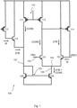
- Figure 1 schematically illustrates a first embodiment 100 of the electronic device according to the present disclosure.
- the third base-emitter voltage VBE3 does not introduce the process variation back into the signal, because its effective process variation is compensated by running the second transistor at the constant base current lB.
- the base current for the bipolar differential pair is injected into the VBG node.
- This node is likely either low-impedance or already compensated for the existing bandgap base current depending on the bandgap topology.
- the electronic device 100 may comprise a branch 104 connected to the emitter of the first transistor 101 and to the emitter of the second transistor 102, such that the branch 104 is configured to carry a summed emitter current, IE.
- This summed emitter current IE may be equal to ⁇ *IB + ICORE, as shown in the figure.
- the electronic device 100 may comprise a current mirror 105 arranged to mirror the summed emitter current, IE.
- the current mirror 105 may comprise:
- the current mirror 105 may further comprise transistors 108 and 109.
- first branch 107 may comprise:
- the first branch 107 may further comprise:
- Figure 2 schematically illustrates a second embodiment 200 of the electronic device according to the present disclosure.
- the electronic device 200 comprises:
- the electronic device 200 may comprise a branch 104 connected to the emitter of the first transistor 101 and to the emitter of the second transistor 102, such that the branch 104 is configured to carry a summed emitter current, IE.
- This summed emitter current IE may be equal to ⁇ *IB + ICORE, as shown in the figure.
- the electronic device 200 may comprise a current mirror 105 arranged to mirror the summed emitter current, IE.
- the current mirror 105 may comprise:
- the current mirror 105 may further comprise transistors 108 and 109.
- first branch 107 may comprise:
- the transistor 204 is thus arranged to generate the scaled base current, i.e. ⁇ *IB. That current goes two places: out of the base to make part of the tail current and through the current mirror to force the second transistor 102 to conduct the same current (once the loop is closed).
- the second embodiment 200 mitigates the risk of mismatch (both random and systematic). Errors in the tail current are less likely to corrupt the current in the second transistor 102. The current through the second transistor 102 will likely be very low at cold and low ⁇ to avoid throwing away current at hot and high ⁇ .
- the second embodiment 200 allows more reasonable current levels to be chosen to achieve a given performance.
- the topology of the embodiments described in the present disclosure also helps to provide a low impedance bandgap reference.
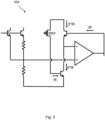
- Figure 3 schematically illustrates a core circuit arranged for supplying the described bandgap voltage reference and various other currents including IB and ⁇ *IB.
- MOSFETs shown in the exemplary first and second embodiments described above are primarily used as mirrors, so the circuit may also be seen as independent of MOSFET type or voltage rating, and the circuit could thus be designed without MOSFETs, using BJTs only.
Landscapes
- Engineering & Computer Science (AREA)
- Physics & Mathematics (AREA)
- Electromagnetism (AREA)
- General Physics & Mathematics (AREA)
- Radar, Positioning & Navigation (AREA)
- Automation & Control Theory (AREA)
- Microelectronics & Electronic Packaging (AREA)
- Power Engineering (AREA)
- Nonlinear Science (AREA)
- Control Of Electrical Variables (AREA)
Applications Claiming Priority (1)
| Application Number | Priority Date | Filing Date | Title |
|---|---|---|---|
| US18/458,658 US12366872B2 (en) | 2023-08-30 | 2023-08-30 | Electronic device with reduced process spread bandgap |
Publications (2)
| Publication Number | Publication Date |
|---|---|
| EP4517475A2 true EP4517475A2 (de) | 2025-03-05 |
| EP4517475A3 EP4517475A3 (de) | 2025-06-25 |
Family
ID=92633095
Family Applications (1)
| Application Number | Title | Priority Date | Filing Date |
|---|---|---|---|
| EP24197502.8A Pending EP4517475A3 (de) | 2023-08-30 | 2024-08-30 | Elektronische vorrichtung mit reduziertem prozessstreuungsbandabstand |
Country Status (3)
| Country | Link |
|---|---|
| US (1) | US12366872B2 (de) |
| EP (1) | EP4517475A3 (de) |
| CN (1) | CN119536434A (de) |
Family Cites Families (5)
| Publication number | Priority date | Publication date | Assignee | Title |
|---|---|---|---|---|
| US4234841A (en) * | 1979-02-05 | 1980-11-18 | Rca Corporation | Self-balancing bridge network |
| JP5957987B2 (ja) * | 2012-03-14 | 2016-07-27 | ミツミ電機株式会社 | バンドギャップリファレンス回路 |
| US20160274617A1 (en) * | 2015-03-17 | 2016-09-22 | Sanjay Kumar Wadhwa | Bandgap circuit |
| EP3671400B1 (de) * | 2018-12-18 | 2022-05-11 | NXP USA, Inc. | Teilbandlückenreferenzspannungsquelle |
| US11086347B1 (en) * | 2020-02-10 | 2021-08-10 | ZJW Microelectronics Limited | Bandgap reference circuit and electronic device |
-
2023
- 2023-08-30 US US18/458,658 patent/US12366872B2/en active Active
-
2024
- 2024-08-27 CN CN202411182152.8A patent/CN119536434A/zh active Pending
- 2024-08-30 EP EP24197502.8A patent/EP4517475A3/de active Pending
Also Published As
| Publication number | Publication date |
|---|---|
| EP4517475A3 (de) | 2025-06-25 |
| US12366872B2 (en) | 2025-07-22 |
| CN119536434A (zh) | 2025-02-28 |
| US20250076908A1 (en) | 2025-03-06 |
Similar Documents
| Publication | Publication Date | Title |
|---|---|---|
| CN102033563B (zh) | 与温度无关的参考电路 | |
| US7166994B2 (en) | Bandgap reference circuits | |
| EP0714055A1 (de) | Stromquelle proportional zur absoluten Temperatur | |
| US10712763B2 (en) | Sub-bandgap reference voltage source | |
| US20040150381A1 (en) | Bandgap reference circuit | |
| JPS61187020A (ja) | 電圧基準回路 | |
| US20140176112A1 (en) | Low voltage bandgap reference circuit | |
| TWI887490B (zh) | 參考電壓電路 | |
| US10795395B2 (en) | Bandgap voltage reference circuit capable of correcting voltage distortion | |
| EP4517475A2 (de) | Elektronische vorrichtung mit reduziertem prozessstreuungsbandabstand | |
| US20200057464A1 (en) | Reference voltage generator circuit generating reference voltage based on band gap by controlling currents flowing in first and second voltage generator circuits | |
| CN112034920B (zh) | 电压产生器 | |
| CN118349074A (zh) | 全氮化镓集成的电压基准电路和电压基准电路控制方法 | |
| US11216021B2 (en) | Current generation circuit | |
| CN120353291B (zh) | 一种低压带隙基准启动电路 | |
| US6856189B2 (en) | Delta Vgs curvature correction for bandgap reference voltage generation | |
| US7633279B2 (en) | Power supply circuit | |
| US6407621B1 (en) | Mechanism for generating precision user-programmable parameters in analog integrated circuit | |
| CN118732774B (zh) | 低温漂无运放的带隙基准电压电路、带隙基准电压的生成方法及补偿方法 | |
| CN116256075B (zh) | 温度感应电路及其芯片、电子设备 | |
| US6201377B1 (en) | Match-insensitive low-current bias circuit | |
| Liao et al. | A sub-1 V high-precision CMOS bandgap voltage reference | |
| Cherry | 2-Terminal floating bandgap voltage reference | |
| US9588538B2 (en) | Reference voltage generation circuit | |
| JP2018185642A (ja) | 基準電圧生成回路 |
Legal Events
| Date | Code | Title | Description |
|---|---|---|---|
| PUAI | Public reference made under article 153(3) epc to a published international application that has entered the european phase |
Free format text: ORIGINAL CODE: 0009012 |
|
| STAA | Information on the status of an ep patent application or granted ep patent |
Free format text: STATUS: THE APPLICATION HAS BEEN PUBLISHED |
|
| AK | Designated contracting states |
Kind code of ref document: A2 Designated state(s): AL AT BE BG CH CY CZ DE DK EE ES FI FR GB GR HR HU IE IS IT LI LT LU LV MC ME MK MT NL NO PL PT RO RS SE SI SK SM TR |
|
| PUAL | Search report despatched |
Free format text: ORIGINAL CODE: 0009013 |
|
| AK | Designated contracting states |
Kind code of ref document: A3 Designated state(s): AL AT BE BG CH CY CZ DE DK EE ES FI FR GB GR HR HU IE IS IT LI LT LU LV MC ME MK MT NL NO PL PT RO RS SE SI SK SM TR |
|
| RIC1 | Information provided on ipc code assigned before grant |
Ipc: G05F 3/30 20060101AFI20250522BHEP |
|
| STAA | Information on the status of an ep patent application or granted ep patent |
Free format text: STATUS: REQUEST FOR EXAMINATION WAS MADE |
|
| 17P | Request for examination filed |
Effective date: 20260105 |