EP4516961A1 - Silicon precursor compound and preparation method therefor, and silicon-containing thin film preparation method using silicon precursor - Google Patents
Silicon precursor compound and preparation method therefor, and silicon-containing thin film preparation method using silicon precursor Download PDFInfo
- Publication number
- EP4516961A1 EP4516961A1 EP23796676.7A EP23796676A EP4516961A1 EP 4516961 A1 EP4516961 A1 EP 4516961A1 EP 23796676 A EP23796676 A EP 23796676A EP 4516961 A1 EP4516961 A1 EP 4516961A1
- Authority
- EP
- European Patent Office
- Prior art keywords
- silicon
- thin film
- precursor compound
- containing thin
- preparing
- Prior art date
- Legal status (The legal status is an assumption and is not a legal conclusion. Google has not performed a legal analysis and makes no representation as to the accuracy of the status listed.)
- Pending
Links
Images



Classifications
-
- C—CHEMISTRY; METALLURGY
- C07—ORGANIC CHEMISTRY
- C07F—ACYCLIC, CARBOCYCLIC OR HETEROCYCLIC COMPOUNDS CONTAINING ELEMENTS OTHER THAN CARBON, HYDROGEN, HALOGEN, OXYGEN, NITROGEN, SULFUR, SELENIUM OR TELLURIUM
- C07F7/00—Compounds containing elements of Groups 4 or 14 of the Periodic Table
- C07F7/02—Silicon compounds
- C07F7/08—Compounds having one or more C—Si linkages
- C07F7/10—Compounds having one or more C—Si linkages containing nitrogen having a Si-N linkage
-
- C—CHEMISTRY; METALLURGY
- C07—ORGANIC CHEMISTRY
- C07F—ACYCLIC, CARBOCYCLIC OR HETEROCYCLIC COMPOUNDS CONTAINING ELEMENTS OTHER THAN CARBON, HYDROGEN, HALOGEN, OXYGEN, NITROGEN, SULFUR, SELENIUM OR TELLURIUM
- C07F7/00—Compounds containing elements of Groups 4 or 14 of the Periodic Table
- C07F7/02—Silicon compounds
- C07F7/025—Silicon compounds without C-silicon linkages
-
- C—CHEMISTRY; METALLURGY
- C07—ORGANIC CHEMISTRY
- C07F—ACYCLIC, CARBOCYCLIC OR HETEROCYCLIC COMPOUNDS CONTAINING ELEMENTS OTHER THAN CARBON, HYDROGEN, HALOGEN, OXYGEN, NITROGEN, SULFUR, SELENIUM OR TELLURIUM
- C07F7/00—Compounds containing elements of Groups 4 or 14 of the Periodic Table
- C07F7/02—Silicon compounds
- C07F7/08—Compounds having one or more C—Si linkages
- C07F7/0803—Compounds with Si-C or Si-Si linkages
- C07F7/081—Compounds with Si-C or Si-Si linkages comprising at least one atom selected from the elements N, O, halogen, S, Se or Te
-
- C—CHEMISTRY; METALLURGY
- C07—ORGANIC CHEMISTRY
- C07F—ACYCLIC, CARBOCYCLIC OR HETEROCYCLIC COMPOUNDS CONTAINING ELEMENTS OTHER THAN CARBON, HYDROGEN, HALOGEN, OXYGEN, NITROGEN, SULFUR, SELENIUM OR TELLURIUM
- C07F7/00—Compounds containing elements of Groups 4 or 14 of the Periodic Table
- C07F7/02—Silicon compounds
- C07F7/08—Compounds having one or more C—Si linkages
- C07F7/12—Organo silicon halides
-
- C—CHEMISTRY; METALLURGY
- C07—ORGANIC CHEMISTRY
- C07F—ACYCLIC, CARBOCYCLIC OR HETEROCYCLIC COMPOUNDS CONTAINING ELEMENTS OTHER THAN CARBON, HYDROGEN, HALOGEN, OXYGEN, NITROGEN, SULFUR, SELENIUM OR TELLURIUM
- C07F7/00—Compounds containing elements of Groups 4 or 14 of the Periodic Table
- C07F7/02—Silicon compounds
- C07F7/08—Compounds having one or more C—Si linkages
- C07F7/12—Organo silicon halides
- C07F7/121—Preparation or treatment not provided for in C07F7/14, C07F7/16 or C07F7/20
-
- C—CHEMISTRY; METALLURGY
- C23—COATING METALLIC MATERIAL; COATING MATERIAL WITH METALLIC MATERIAL; CHEMICAL SURFACE TREATMENT; DIFFUSION TREATMENT OF METALLIC MATERIAL; COATING BY VACUUM EVAPORATION, BY SPUTTERING, BY ION IMPLANTATION OR BY CHEMICAL VAPOUR DEPOSITION, IN GENERAL; INHIBITING CORROSION OF METALLIC MATERIAL OR INCRUSTATION IN GENERAL
- C23C—COATING METALLIC MATERIAL; COATING MATERIAL WITH METALLIC MATERIAL; SURFACE TREATMENT OF METALLIC MATERIAL BY DIFFUSION INTO THE SURFACE, BY CHEMICAL CONVERSION OR SUBSTITUTION; COATING BY VACUUM EVAPORATION, BY SPUTTERING, BY ION IMPLANTATION OR BY CHEMICAL VAPOUR DEPOSITION, IN GENERAL
- C23C16/00—Chemical coating by decomposition of gaseous compounds, without leaving reaction products of surface material in the coating, i.e. chemical vapour deposition [CVD] processes
- C23C16/22—Chemical coating by decomposition of gaseous compounds, without leaving reaction products of surface material in the coating, i.e. chemical vapour deposition [CVD] processes characterised by the deposition of inorganic material, other than metallic material
- C23C16/30—Deposition of compounds, mixtures or solid solutions, e.g. borides, carbides, nitrides
-
- C—CHEMISTRY; METALLURGY
- C23—COATING METALLIC MATERIAL; COATING MATERIAL WITH METALLIC MATERIAL; CHEMICAL SURFACE TREATMENT; DIFFUSION TREATMENT OF METALLIC MATERIAL; COATING BY VACUUM EVAPORATION, BY SPUTTERING, BY ION IMPLANTATION OR BY CHEMICAL VAPOUR DEPOSITION, IN GENERAL; INHIBITING CORROSION OF METALLIC MATERIAL OR INCRUSTATION IN GENERAL
- C23C—COATING METALLIC MATERIAL; COATING MATERIAL WITH METALLIC MATERIAL; SURFACE TREATMENT OF METALLIC MATERIAL BY DIFFUSION INTO THE SURFACE, BY CHEMICAL CONVERSION OR SUBSTITUTION; COATING BY VACUUM EVAPORATION, BY SPUTTERING, BY ION IMPLANTATION OR BY CHEMICAL VAPOUR DEPOSITION, IN GENERAL
- C23C16/00—Chemical coating by decomposition of gaseous compounds, without leaving reaction products of surface material in the coating, i.e. chemical vapour deposition [CVD] processes
- C23C16/22—Chemical coating by decomposition of gaseous compounds, without leaving reaction products of surface material in the coating, i.e. chemical vapour deposition [CVD] processes characterised by the deposition of inorganic material, other than metallic material
- C23C16/30—Deposition of compounds, mixtures or solid solutions, e.g. borides, carbides, nitrides
- C23C16/308—Oxynitrides
-
- C—CHEMISTRY; METALLURGY
- C23—COATING METALLIC MATERIAL; COATING MATERIAL WITH METALLIC MATERIAL; CHEMICAL SURFACE TREATMENT; DIFFUSION TREATMENT OF METALLIC MATERIAL; COATING BY VACUUM EVAPORATION, BY SPUTTERING, BY ION IMPLANTATION OR BY CHEMICAL VAPOUR DEPOSITION, IN GENERAL; INHIBITING CORROSION OF METALLIC MATERIAL OR INCRUSTATION IN GENERAL
- C23C—COATING METALLIC MATERIAL; COATING MATERIAL WITH METALLIC MATERIAL; SURFACE TREATMENT OF METALLIC MATERIAL BY DIFFUSION INTO THE SURFACE, BY CHEMICAL CONVERSION OR SUBSTITUTION; COATING BY VACUUM EVAPORATION, BY SPUTTERING, BY ION IMPLANTATION OR BY CHEMICAL VAPOUR DEPOSITION, IN GENERAL
- C23C16/00—Chemical coating by decomposition of gaseous compounds, without leaving reaction products of surface material in the coating, i.e. chemical vapour deposition [CVD] processes
- C23C16/22—Chemical coating by decomposition of gaseous compounds, without leaving reaction products of surface material in the coating, i.e. chemical vapour deposition [CVD] processes characterised by the deposition of inorganic material, other than metallic material
- C23C16/30—Deposition of compounds, mixtures or solid solutions, e.g. borides, carbides, nitrides
- C23C16/32—Carbides
- C23C16/325—Silicon carbide
-
- C—CHEMISTRY; METALLURGY
- C23—COATING METALLIC MATERIAL; COATING MATERIAL WITH METALLIC MATERIAL; CHEMICAL SURFACE TREATMENT; DIFFUSION TREATMENT OF METALLIC MATERIAL; COATING BY VACUUM EVAPORATION, BY SPUTTERING, BY ION IMPLANTATION OR BY CHEMICAL VAPOUR DEPOSITION, IN GENERAL; INHIBITING CORROSION OF METALLIC MATERIAL OR INCRUSTATION IN GENERAL
- C23C—COATING METALLIC MATERIAL; COATING MATERIAL WITH METALLIC MATERIAL; SURFACE TREATMENT OF METALLIC MATERIAL BY DIFFUSION INTO THE SURFACE, BY CHEMICAL CONVERSION OR SUBSTITUTION; COATING BY VACUUM EVAPORATION, BY SPUTTERING, BY ION IMPLANTATION OR BY CHEMICAL VAPOUR DEPOSITION, IN GENERAL
- C23C16/00—Chemical coating by decomposition of gaseous compounds, without leaving reaction products of surface material in the coating, i.e. chemical vapour deposition [CVD] processes
- C23C16/22—Chemical coating by decomposition of gaseous compounds, without leaving reaction products of surface material in the coating, i.e. chemical vapour deposition [CVD] processes characterised by the deposition of inorganic material, other than metallic material
- C23C16/30—Deposition of compounds, mixtures or solid solutions, e.g. borides, carbides, nitrides
- C23C16/34—Nitrides
- C23C16/345—Silicon nitride
-
- C—CHEMISTRY; METALLURGY
- C23—COATING METALLIC MATERIAL; COATING MATERIAL WITH METALLIC MATERIAL; CHEMICAL SURFACE TREATMENT; DIFFUSION TREATMENT OF METALLIC MATERIAL; COATING BY VACUUM EVAPORATION, BY SPUTTERING, BY ION IMPLANTATION OR BY CHEMICAL VAPOUR DEPOSITION, IN GENERAL; INHIBITING CORROSION OF METALLIC MATERIAL OR INCRUSTATION IN GENERAL
- C23C—COATING METALLIC MATERIAL; COATING MATERIAL WITH METALLIC MATERIAL; SURFACE TREATMENT OF METALLIC MATERIAL BY DIFFUSION INTO THE SURFACE, BY CHEMICAL CONVERSION OR SUBSTITUTION; COATING BY VACUUM EVAPORATION, BY SPUTTERING, BY ION IMPLANTATION OR BY CHEMICAL VAPOUR DEPOSITION, IN GENERAL
- C23C16/00—Chemical coating by decomposition of gaseous compounds, without leaving reaction products of surface material in the coating, i.e. chemical vapour deposition [CVD] processes
- C23C16/22—Chemical coating by decomposition of gaseous compounds, without leaving reaction products of surface material in the coating, i.e. chemical vapour deposition [CVD] processes characterised by the deposition of inorganic material, other than metallic material
- C23C16/30—Deposition of compounds, mixtures or solid solutions, e.g. borides, carbides, nitrides
- C23C16/36—Carbonitrides
-
- C—CHEMISTRY; METALLURGY
- C23—COATING METALLIC MATERIAL; COATING MATERIAL WITH METALLIC MATERIAL; CHEMICAL SURFACE TREATMENT; DIFFUSION TREATMENT OF METALLIC MATERIAL; COATING BY VACUUM EVAPORATION, BY SPUTTERING, BY ION IMPLANTATION OR BY CHEMICAL VAPOUR DEPOSITION, IN GENERAL; INHIBITING CORROSION OF METALLIC MATERIAL OR INCRUSTATION IN GENERAL
- C23C—COATING METALLIC MATERIAL; COATING MATERIAL WITH METALLIC MATERIAL; SURFACE TREATMENT OF METALLIC MATERIAL BY DIFFUSION INTO THE SURFACE, BY CHEMICAL CONVERSION OR SUBSTITUTION; COATING BY VACUUM EVAPORATION, BY SPUTTERING, BY ION IMPLANTATION OR BY CHEMICAL VAPOUR DEPOSITION, IN GENERAL
- C23C16/00—Chemical coating by decomposition of gaseous compounds, without leaving reaction products of surface material in the coating, i.e. chemical vapour deposition [CVD] processes
- C23C16/22—Chemical coating by decomposition of gaseous compounds, without leaving reaction products of surface material in the coating, i.e. chemical vapour deposition [CVD] processes characterised by the deposition of inorganic material, other than metallic material
- C23C16/30—Deposition of compounds, mixtures or solid solutions, e.g. borides, carbides, nitrides
- C23C16/40—Oxides
- C23C16/401—Oxides containing silicon
- C23C16/402—Silicon dioxide
-
- C—CHEMISTRY; METALLURGY
- C23—COATING METALLIC MATERIAL; COATING MATERIAL WITH METALLIC MATERIAL; CHEMICAL SURFACE TREATMENT; DIFFUSION TREATMENT OF METALLIC MATERIAL; COATING BY VACUUM EVAPORATION, BY SPUTTERING, BY ION IMPLANTATION OR BY CHEMICAL VAPOUR DEPOSITION, IN GENERAL; INHIBITING CORROSION OF METALLIC MATERIAL OR INCRUSTATION IN GENERAL
- C23C—COATING METALLIC MATERIAL; COATING MATERIAL WITH METALLIC MATERIAL; SURFACE TREATMENT OF METALLIC MATERIAL BY DIFFUSION INTO THE SURFACE, BY CHEMICAL CONVERSION OR SUBSTITUTION; COATING BY VACUUM EVAPORATION, BY SPUTTERING, BY ION IMPLANTATION OR BY CHEMICAL VAPOUR DEPOSITION, IN GENERAL
- C23C16/00—Chemical coating by decomposition of gaseous compounds, without leaving reaction products of surface material in the coating, i.e. chemical vapour deposition [CVD] processes
- C23C16/44—Chemical coating by decomposition of gaseous compounds, without leaving reaction products of surface material in the coating, i.e. chemical vapour deposition [CVD] processes characterised by the method of coating
- C23C16/4401—Means for minimising impurities, e.g. dust, moisture or residual gas, in the reaction chamber
- C23C16/4408—Means for minimising impurities, e.g. dust, moisture or residual gas, in the reaction chamber by purging residual gases from the reaction chamber or gas lines
-
- C—CHEMISTRY; METALLURGY
- C23—COATING METALLIC MATERIAL; COATING MATERIAL WITH METALLIC MATERIAL; CHEMICAL SURFACE TREATMENT; DIFFUSION TREATMENT OF METALLIC MATERIAL; COATING BY VACUUM EVAPORATION, BY SPUTTERING, BY ION IMPLANTATION OR BY CHEMICAL VAPOUR DEPOSITION, IN GENERAL; INHIBITING CORROSION OF METALLIC MATERIAL OR INCRUSTATION IN GENERAL
- C23C—COATING METALLIC MATERIAL; COATING MATERIAL WITH METALLIC MATERIAL; SURFACE TREATMENT OF METALLIC MATERIAL BY DIFFUSION INTO THE SURFACE, BY CHEMICAL CONVERSION OR SUBSTITUTION; COATING BY VACUUM EVAPORATION, BY SPUTTERING, BY ION IMPLANTATION OR BY CHEMICAL VAPOUR DEPOSITION, IN GENERAL
- C23C16/00—Chemical coating by decomposition of gaseous compounds, without leaving reaction products of surface material in the coating, i.e. chemical vapour deposition [CVD] processes
- C23C16/44—Chemical coating by decomposition of gaseous compounds, without leaving reaction products of surface material in the coating, i.e. chemical vapour deposition [CVD] processes characterised by the method of coating
- C23C16/455—Chemical coating by decomposition of gaseous compounds, without leaving reaction products of surface material in the coating, i.e. chemical vapour deposition [CVD] processes characterised by the method of coating characterised by the method used for introducing gases into reaction chamber or for modifying gas flows in reaction chamber
- C23C16/45523—Pulsed gas flow or change of composition over time
- C23C16/45525—Atomic layer deposition [ALD]
- C23C16/45527—Atomic layer deposition [ALD] characterized by the ALD cycle, e.g. different flows or temperatures during half-reactions, unusual pulsing sequence, use of precursor mixtures or auxiliary reactants or activations
- C23C16/45536—Use of plasma, radiation or electromagnetic fields
-
- C—CHEMISTRY; METALLURGY
- C23—COATING METALLIC MATERIAL; COATING MATERIAL WITH METALLIC MATERIAL; CHEMICAL SURFACE TREATMENT; DIFFUSION TREATMENT OF METALLIC MATERIAL; COATING BY VACUUM EVAPORATION, BY SPUTTERING, BY ION IMPLANTATION OR BY CHEMICAL VAPOUR DEPOSITION, IN GENERAL; INHIBITING CORROSION OF METALLIC MATERIAL OR INCRUSTATION IN GENERAL
- C23C—COATING METALLIC MATERIAL; COATING MATERIAL WITH METALLIC MATERIAL; SURFACE TREATMENT OF METALLIC MATERIAL BY DIFFUSION INTO THE SURFACE, BY CHEMICAL CONVERSION OR SUBSTITUTION; COATING BY VACUUM EVAPORATION, BY SPUTTERING, BY ION IMPLANTATION OR BY CHEMICAL VAPOUR DEPOSITION, IN GENERAL
- C23C16/00—Chemical coating by decomposition of gaseous compounds, without leaving reaction products of surface material in the coating, i.e. chemical vapour deposition [CVD] processes
- C23C16/44—Chemical coating by decomposition of gaseous compounds, without leaving reaction products of surface material in the coating, i.e. chemical vapour deposition [CVD] processes characterised by the method of coating
- C23C16/455—Chemical coating by decomposition of gaseous compounds, without leaving reaction products of surface material in the coating, i.e. chemical vapour deposition [CVD] processes characterised by the method of coating characterised by the method used for introducing gases into reaction chamber or for modifying gas flows in reaction chamber
- C23C16/45523—Pulsed gas flow or change of composition over time
- C23C16/45525—Atomic layer deposition [ALD]
- C23C16/45527—Atomic layer deposition [ALD] characterized by the ALD cycle, e.g. different flows or temperatures during half-reactions, unusual pulsing sequence, use of precursor mixtures or auxiliary reactants or activations
- C23C16/45536—Use of plasma, radiation or electromagnetic fields
- C23C16/45542—Plasma being used non-continuously during the ALD reactions
-
- C—CHEMISTRY; METALLURGY
- C23—COATING METALLIC MATERIAL; COATING MATERIAL WITH METALLIC MATERIAL; CHEMICAL SURFACE TREATMENT; DIFFUSION TREATMENT OF METALLIC MATERIAL; COATING BY VACUUM EVAPORATION, BY SPUTTERING, BY ION IMPLANTATION OR BY CHEMICAL VAPOUR DEPOSITION, IN GENERAL; INHIBITING CORROSION OF METALLIC MATERIAL OR INCRUSTATION IN GENERAL
- C23C—COATING METALLIC MATERIAL; COATING MATERIAL WITH METALLIC MATERIAL; SURFACE TREATMENT OF METALLIC MATERIAL BY DIFFUSION INTO THE SURFACE, BY CHEMICAL CONVERSION OR SUBSTITUTION; COATING BY VACUUM EVAPORATION, BY SPUTTERING, BY ION IMPLANTATION OR BY CHEMICAL VAPOUR DEPOSITION, IN GENERAL
- C23C16/00—Chemical coating by decomposition of gaseous compounds, without leaving reaction products of surface material in the coating, i.e. chemical vapour deposition [CVD] processes
- C23C16/44—Chemical coating by decomposition of gaseous compounds, without leaving reaction products of surface material in the coating, i.e. chemical vapour deposition [CVD] processes characterised by the method of coating
- C23C16/455—Chemical coating by decomposition of gaseous compounds, without leaving reaction products of surface material in the coating, i.e. chemical vapour deposition [CVD] processes characterised by the method of coating characterised by the method used for introducing gases into reaction chamber or for modifying gas flows in reaction chamber
- C23C16/45523—Pulsed gas flow or change of composition over time
- C23C16/45525—Atomic layer deposition [ALD]
- C23C16/45553—Atomic layer deposition [ALD] characterized by the use of precursors specially adapted for ALD
Definitions
- the present invention relates to a silicon precursor compound, to a method for preparing the same, and to a method for preparing a silicon-containing thin film using a silicon precursor compound.
- Silicon-containing thin films such as films of silicon oxide, silicon nitride, silicon oxynitride, and silicon carbonitride, are those among the thin films that are essential for operating microelectronic devices such as semiconductors as well as non-semiconductor (logic).
- Atomic layer deposition or chemical vapor deposition (CVD) is widely used to prepare silicon-containing thin films.
- Atomic layer deposition (ALD) among the above is a method that sequentially supplies a silicon compound gas and a reactant gas necessary for film formation, and it has the advantage of being able to form a silicon-containing thin film with a uniform thickness even on a highly uneven surface.
- atomic layer deposition is widely utilized.
- Si precursors used in the preparation of silicon-containing thin films are of various types depending on various process conditions and their physical and chemical properties.
- Another object is to provide a method for preparing a silicon-containing thin film using such a silicon precursor compound.
- the silicon precursor compound of the present invention for accomplishing the above object is characterized in that it is represented by the following Formula 1.
- R 0 , R 5 , and R 6 are each independently a linear or branched, saturated or unsaturated hydrocarbon group having 1 to 4 carbon atoms or an isomer thereof
- R 1 , R 2 , R 3 , and R 4 are each independently hydrogen (H), a halogen, or a linear or branched, saturated or unsaturated hydrocarbon group having 1 to 4 carbon atoms
- X is hydrogen (H) or a halogen.
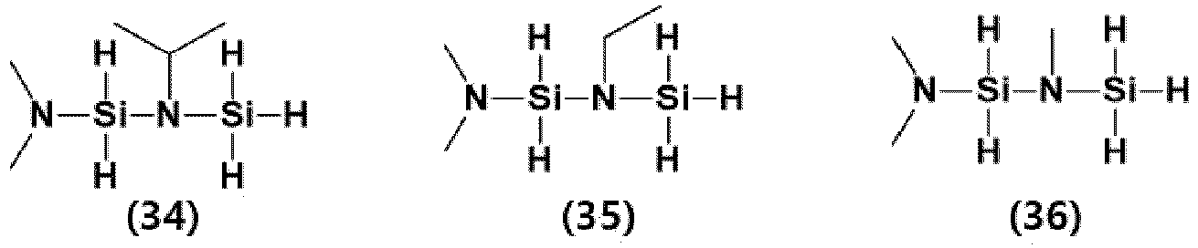
- the silicon precursor compound of the present invention is preferably selected from the following compounds (1) to (36).
- the method for preparing a silicon precursor compound of the present invention may comprise a first step of reacting a chlorosilane derivative with a primary amine to form a first compound, a second step of reacting the first compound with an alkyl-lithium (Alkyl-Li) to form a second compound comprising lithium, and a third step of reacting the second compound with a silane compound to prepare a silicon precursor compound represented by Formula 1.
- the first compound is preferably a compound represented by the following Formula 7.
- R 0 is each independently a linear or branched, saturated or unsaturated hydrocarbon group having 1 to 4 carbon atoms or an isomer thereof; and R 2 , R 3 , and R 4 are each independently hydrogen (H), a halogen, or a linear or branched, saturated or unsaturated hydrocarbon group having 1 to 4 carbon atoms.
- X and R 1 in the silicon precursor compound represented by Formula 1 are each a halogen, it may comprise a fourth step of reacting it with a metal hydride (MH).
- the silane compound may be produced by reacting a chlorosilane derivative with a secondary amine.
- the silicon precursor compound of Formula 1 prepared according to the method for preparing a silicon precursor compound of the present invention is selected from the above compounds (1) to (36).
- the method for preparing a silicon-containing thin film according to the present invention may form a silicon-containing thin film using the silicon precursor compound represented by Formula 1.
- the silicon precursor compound is preferably selected from the above compounds (1) to (36).
- the silicon-containing thin film may be deposited by chemical vapor deposition (CVD) or atomic layer deposition (ALD).
- the atomic layer deposition in the present invention may comprise plasma-enhanced atomic layer deposition.
- the silicon-containing thin film may be any one selected from the group consisting of a silicon oxide film (SiO 2 ), a silicon oxycarbide film (SiOC), a silicon nitride film (SiN), a silicon oxynitride film (SiON), a silicon carbonitride film (SiCN), and a silicon carbonized film (SiC).
- a silicon oxide film SiO 2
- SiOC silicon oxycarbide film
- SiN silicon nitride film
- SiON silicon oxynitride film
- SiCN silicon carbonitride film
- SiC silicon carbonized film
- the silicon-containing thin film according to the present invention may be formed at a temperature of about 500°C or lower.
- a silicon oxide (SiO 2 ) film may be formed by atomic layer deposition.
- the atomic layer deposition according to an embodiment comprises providing a substrate to a reactor; introducing the silicon precursor compound according to the present invention into the reactor; purging the reactor with a purge gas; introducing an oxygen source into the reactor to react with the silicon precursor compound according to the present invention to form a silicon oxide film; and purging the reactor with the purge gas.
- the purge gas according to an embodiment is used to remove unconsumed reactants and reaction by-products and is preferably selected from the group consisting of nitrogen, helium, argon, and mixtures thereof, but it is not limited thereto.
- the oxygen source according to an embodiment is preferably selected from the group consisting of oxygen, peroxide, oxygen plasma, water vapor, water vapor plasma, hydrogen peroxide, ozone source, and mixtures thereof, but it is not limited thereto.
- the oxygen source may comprise plasma, and the plasma may be generated in situ.
- the atomic layer deposition according to an embodiment may be carried out at one or more temperatures of about 500°C or lower.
- the lower limit of the temperature may be appropriately selected by a person of ordinary skill in the art depending on the type of oxygen source used.
- a silicon oxide film may be formed at one or more temperatures of about 300°C to 500°C.
- a silicon nitride (SiN) film may be formed by plasma-enhanced atomic layer deposition.
- the atomic layer deposition according to an embodiment comprises providing a substrate to a reactor; introducing the silicon precursor compound according to the present invention into the reactor; purging the reactor with a purge gas; introducing a nitrogen-containing plasma source and an inert gas into the reactor to react with the silicon precursor compound according to the present invention to form a silicon nitride film; and purging the reactor with the purge gas.
- the purge gas according to an embodiment is used to remove unconsumed reactants and reaction by-products and is preferably selected from the group consisting of nitrogen, helium, argon, and mixtures thereof, but it is not limited thereto.
- the plasma-enhanced atomic layer deposition according to an embodiment may be carried out at one or more temperatures of about 400°C or lower.
- the lower limit of the temperature may be appropriately selected by a person of ordinary skill in the art depending on the type of nitrogen-containing plasma source used.
- a silicon nitride film may be formed at one or more temperatures of about 150°C to 350°C, more preferably, at a temperature of about 250°C.
- the silicon precursor compound of the present invention exhibits sufficient volatility to be applied to both atomic layer deposition (ALD) and chemical vapor deposition (CVD) for preparing silicon-containing thin films.
- ALD atomic layer deposition
- CVD chemical vapor deposition
- the silicon precursor compound of the present invention may be represented by the following Formula 1.
- R 0 , R 5 , and R 6 are each independently a linear or branched, saturated or unsaturated hydrocarbon group having 1 to 4 carbon atoms or an isomer thereof
- R 1 , R 2 , R 3 , and R 4 are each independently hydrogen (H), a halogen, or a linear or branched, saturated or unsaturated hydrocarbon group having 1 to 4 carbon atoms
- X is hydrogen (H) or a halogen.
- the hydrocarbon groups in R 0 , R 1 , R 2 , R 3 , R 4 , R 5 , and R 6 may each independently be any one selected from the group consisting of a methyl group, an ethyl group, an n-propyl group, an iso-propyl group, an n-butyl group, an iso-butyl group, a sec-butyl group, a tert-butyl group, and isomers thereof.
- the halogen may be any one selected from the group consisting of chlorine (CI), bromine (Br), iodine (I), and fluorine (F). Chlorine (CI) is preferable among the above.
- R 0 is any one selected from a methyl group (Me), an ethyl group (Et), and an iso-propyl group ( iso Pr)
- R 1 , R 2 , R 3 , and R 4 are each independently any one selected from hydrogen (H), chlorine (CI), and a methyl group (Me)
- R 5 and R 6 are each independently a methyl group (Me) or an ethyl group (Et)
- X is hydrogen (H) or chlorine (CI).
- the silicon precursor compound of the present invention may be prepared by a method as shown in Reaction Scheme 1 or Reaction Scheme 2 below.
- the method for preparing a silicon precursor compound according to Reaction Scheme 1 may be carried out in a sequence of a first step of reacting a chlorosilane derivative represented by Formula 5 with a primary amine represented by Formula 6 to form a first compound represented by Formula 7, a second step of reacting the first compound with an alkyl-lithium (Alkyl-Li) to form a second compound represented by Formula 8, and a third step of reacting the second compound with a silane compound represented by Formula 4 to prepare a silicon precursor compound represented by Formula 1.
- first compound and the second compound are terms used only for the purpose of distinguishing the compounds formed at each step in the method for preparing a silicon precursor compound.
- a triorganochlorosilane as a chlorosilane derivative is reacted with a primary amine at a low temperature of about -40°C in a non-polar solvent to perform a substitution reaction of Cl and an amine, followed by filtration and distillation under a reduced pressure to form a compound of Formula 7.
- the compound of Formula 7 formed in the first step is reacted with an alkyl-lithium (alkyl-Li) at a low temperature of about -40°C in a non-polar solvent to perform a Li substitution reaction to form a compound of Formula 8.
- alkyl-Li alkyl-lithium
- the alkyl-Li is lithium containing an alkyl group having 1 to 10 carbon atoms. Examples thereof include methyl lithium, ethyl lithium, propyl lithium, butyl lithium, and isobutyl lithium.
- the salt (LiCl) as a product of the reaction and unreacted substances are removed through filtration, and distillation under a reduced pressure is performed to obtain a silicon precursor compound represented by Formula 1.
- Another method for preparing a silicon precursor compound according to Reaction Scheme 2 may be carried out in the same manner as in Reaction Scheme 1.
- X and R 1 in the silicon precursor compound represented by Formula 1' in Reaction Scheme 2 are each a halogen selected from fluorine (F), chlorine (CI), bromine (Br), or iodine (I)
- a fourth step of reacting with a metal hydride (MH) as a reducing agent is further carried out.
- the metal hydride (MH) may be at least one selected from lithium hydride (LiH), sodium hydride (NaH), lithium boron hydride (LiBH 4 ), lithium aluminum hydride (LiAlH 4 ), sodium aluminum hydride (NaAlH 4 ), and sodium boron hydride (NaBH 4 ).
- lithium hydride (LiH) as a metal hydride (MH) may be used by reacting with tetrahydrofuran (THF).
- the fourth step is carried out when X and R 1 in Formula 1' are chlorine (CI).
- a chlorosilane derivative represented by Formula 2 is reacted with a secondary amine of Formula 3 at a low temperature of about -40°C in a non-polar solvent to perform a substitution reaction of Cl and an amine, followed by filtration and distillation under a reduced pressure to form a compound of Formula 4.
- R 0 , R 5 , and R 6 are each independently a linear or branched, saturated or unsaturated hydrocarbon group having 1 to 4 carbon atoms or an isomer thereof
- R 1 , R 2 , R 3 , and R 4 are each independently hydrogen (H), a halogen, or a linear or branched, saturated or unsaturated hydrocarbon group having 1 to 4 carbon atoms
- X is hydrogen (H) or a halogen.
- R 0 may be any one selected from a methyl group (Me), an ethyl group (Et), and an iso-propyl group ( iso Pr)
- R 1 , R 2 , R 3 , and R 4 may each independently be any one selected from hydrogen (H), chlorine (CI), and a methyl group (Me)
- R 5 and R 6 may each independently be a methyl group (Me) or an ethyl group (Et)
- X may be hydrogen (H) or chlorine (CI).
- non-polar solvent used in Reaction Schemes 1 to 3 hexane, n-pentane, or the like may be used, but it is not limited thereto.
- a non-polar solvent commonly used by a person of ordinary skill in the art can be used.
- the silicon precursor compound of the present invention is selected from the following compounds (1) to (36).
- a silicon-containing thin film can be formed using the silicon precursor compound represented by Formula 1 by chemical vapor deposition (CVD) or atomic layer deposition (ALD).
- CVD chemical vapor deposition
- ALD atomic layer deposition
- the silicon-containing thin film may be formed as any one selected from the group consisting of a silicon oxide film (SiO 2 ), a silicon oxycarbide film (SiOC), a silicon nitride film (SiN), a silicon oxynitride film (SiON), a silicon carbonitride film (SiCN), and a silicon carbonized film (SiC).
- a silicon oxide film SiO 2
- SiOC silicon oxycarbide film
- SiN silicon nitride film
- SiON silicon oxynitride film
- SiCN silicon carbonitride film
- SiC silicon carbonized film
- isopropylaminotrimethylsilazane was prepared.
- a 1-liter flask in an anhydrous and inert atmosphere was charged with 220 g (2.03 moles) of chlorotrimethylsilane ((CH 3 ) 3 SiCl) and 2,190 g (30 moles) of n-pentane. While the temperature was maintained at -40°C, 251 g (4.25 moles) of isopropylamine ((CH 3 ) 2 CHNH 2 ) was slowly added, followed by stirring for 3 hours.
- Fig. 1 shows a hydrogen nuclear magnetic resonance ( 1 H-NMR) spectrum of the silicon precursor compound prepared according to Example 1 of the present invention. As shown in Fig. 1 , the silicon precursor compound prepared in Example 1 was confirmed to be diethylaminoisopropyltetramethyldisilazane.
- Example 2 dimethylaminoisopropyltetramethyldisilazane of compound (13) was prepared as a silicon precursor compound.
- Example 2 In the second step of Example 2, a 1-liter flask in an anhydrous and inert atmosphere was charged with 220 g (1.51 moles) of isopropylaminotrimethylsilazane ((CH 3 ) 2 CHNHSi(CH 3 ) 3 ) prepared in the first step and 1,304 g (15.1 moles) of hexane. While the temperature was maintained at -40°C, 641 ml (1.59 mole) of 2.5 M n-butyllithium (n-BuLi) was slowly added. The temperature of the reaction solution was then gradually raised to room temperature, followed by stirring for 12 hours at room temperature.
- isopropylaminotrimethylsilazane ((CH 3 ) 2 CHNHSi(CH 3 ) 3 ) prepared in the first step
- 1,304 g (15.1 moles) of hexane 1,304 g (15.1 moles) of hexane. While the temperature was maintained at -40°C, 641 ml (1.
- Fig. 2 shows a hydrogen nuclear magnetic resonance ( 1 H-NMR) spectrum of the silicon precursor compound prepared according to Example 2 of the present invention. As shown in Fig. 2 , the silicon precursor compound prepared in Example 2 was confirmed to be dimethylaminoisopropyltetramethyldisilazane.
- Example 3 chloro-isopropyl-dimethyl-(trimethylsilyl)silane diamine of compound (16) was prepared as a silicon precursor compound.
- Example 3 In the second step of Example 3, a 1-liter flask in an anhydrous and inert atmosphere was charged with 200 g (1.38 moles) of isopropylaminotrimethylsilazane ((CH 3 ) 2 CHNHSi(CH 3 ) 3 ) prepared in the first step and 593 g (6.88 moles) of hexane. While the temperature was maintained at -40°C, 402 ml (1.45 mole) of 2.5 M n-butyllithium (n-BuLi) was slowly added. The temperature of the reaction solution was then gradually raised to room temperature, followed by stirring for 12 hours at room temperature.
- isopropylaminotrimethylsilazane ((CH 3 ) 2 CHNHSi(CH 3 ) 3 ) prepared in the first step
- 593 g (6.88 moles) of hexane While the temperature was maintained at -40°C, 402 ml (1.45 mole) of 2.5 M n-butyllithium
- Example 4 isopropyldimethyltrimethylsilylsilanediamine of compound (19) was prepared as a silicon precursor compound.
- chloro-isopropyl-dimethyl-(trimethylsilyl)silane diamine ((CH 3 ) 2 NHClSiNCH 2 (CH 3 ) 2 Si(CH 3 ) 3 ) required for the preparation of a silicon precursor compound was prepared in the same manner as in Example 3.
- Thermogravimetric analysis was carried out to analyze the thermal characteristics of the silicon precursor compounds prepared in Examples 1 and 2. The results are shown in Fig. 3 .
- the silicon precursor compound of Example 1 shows volatility in various temperature ranges of 200°C or lower, between 200°C and 500°C, and 500°C or higher.
- the silicon precursor compound of Example 2 shows volatility in the temperature ranges of 160°C or lower, between 160°C to 500°C, and 500°C or higher, which are lower than the temperature ranges of Example 1.
- they are excellent silicon precursors capable of forming a silicon-containing oxide thin film and a silicon-containing nitride thin film in a wide range of temperatures.
- Example 2 shows a higher vapor pressure at a lower temperature than Example 1.
- a silicon nitride thin film was deposited on a silicon substrate by atomic layer deposition (ALD) using diethylaminoisopropyltetramethyldisilazane of Example 1 as a silicon precursor compound.
- ALD atomic layer deposition
- diethylaminoisopropyltetramethyldisilazane of Example 1 as a silicon precursor compound.
- an ALD reactor in which a silicon precursor compound and a reactive gas are separately supplied in a vertical direction using a double shower head was used.
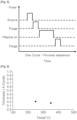
- Table 1 and Fig. 9 show the specific conditions for silicon nitride thin film deposition.
- Source Substrate Temp. Precursor heating Precursor injection Purge N 2 plasma Purge No. of depositions Unit °C °C Time (sec.) Flow rate (sccm) Time (sec.) Flow rate (sccm) Time (sec.) Flow rate (sccm) Time (sec.) Ex. 1 150-350 60 7 300 7 1,000 7 300 9 100
- Fig. 6 is a graph showing the deposition rate of a silicon nitride thin film with respect to the substrate temperature. As shown in Fig. 6 , the deposition rates were similar under the conditions of 250°C and 350°C.
- a silicon oxide film (SiO 2 ) formed using a silicon precursor compound prepared according to the present invention
- a silicon oxide film was deposited on a silicon substrate by atomic layer deposition (ALD) using dimethylaminoisopropyltetramethyldisilazane of Example 2 as a silicon precursor compound.
- ALD atomic layer deposition
- an atomic layer deposition (ALD) reactor in which a silicon precursor compound and a reactive gas are separately supplied in a vertical direction using a double shower head was used.
- silicon-containing thin films SiN and SiO 2 , are prepared and described as a representative example, but it is not limited thereto.
- Silicon-containing thin films known in the art such as SiN, SiO 2 , SiOC, SiON, SiCN, and SiC can be formed.
- Table 3 and Fig. 7 show the specific conditions for silicon oxide film deposition.
- Source Substrate Temp. Precursor heating Precursor injection Purge O 2 plasma/200 W Purge No. of depositions Unit °C °C Time (sec.) Flow rate (sccm) Time (sec.) Flow rate (sccm) Time (sec.) Flow rate (sccm) Time (sec.) Ex. 2 300-500 60 7 1,000 8 1,000 5 1,000 10 100
- composition of the silicon oxide film was analyzed using X-ray photoelectron spectroscopy (XPS) of the thin film deposited by the above method, and the step coating was confirmed using transmission electron microscopy (TEM).
- Table 4 and Figs. 8 and 9 show the results of analyzing the characteristics of the specific silicon oxide film.
- Table 4 Source Substrate temp. Deposition rate Film thickness O/Si °C ⁇ /cycle ⁇ Composition ratio Example 2 400 0.99 90 1.7
- the silicon oxide film formed using the silicon precursor compound of Example 2 had a thick film thickness of 90 ⁇ , and a silicon-containing thin film with high purity was formed when the composition ratio of O/Si was examined.
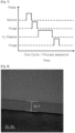
- Fig. 8 is a transmission electron microscope (TEM) photograph of a silicon oxide film deposited at a substrate temperature of 400°C. As shown in Fig. 8 , a silicon oxide film was formed uniformly with a thickness of 90 ⁇ .
- TEM transmission electron microscope
- Fig. 9 is a graph showing the deposition rate of a silicon oxide film with respect to the substrate temperature. As shown in Fig. 9 , the deposition rates were similar in the temperature range of 300°C and 500°C.
- the cyclodisilazane derivatives prepared according to the present invention as a silicon precursor compound are suitable for forming a silicon-containing thin film with high purity at a high deposition rate through atomic layer deposition (ALD).
- ALD atomic layer deposition
Landscapes
- Chemical & Material Sciences (AREA)
- Organic Chemistry (AREA)
- Engineering & Computer Science (AREA)
- Metallurgy (AREA)
- General Chemical & Material Sciences (AREA)
- Chemical Kinetics & Catalysis (AREA)
- Materials Engineering (AREA)
- Mechanical Engineering (AREA)
- Inorganic Chemistry (AREA)
- Plasma & Fusion (AREA)
- Physics & Mathematics (AREA)
- Electromagnetism (AREA)
- Chemical Vapour Deposition (AREA)
- Formation Of Insulating Films (AREA)
Abstract
Description
- The present invention relates to a silicon precursor compound, to a method for preparing the same, and to a method for preparing a silicon-containing thin film using a silicon precursor compound.
- Silicon-containing thin films, such as films of silicon oxide, silicon nitride, silicon oxynitride, and silicon carbonitride, are those among the thin films that are essential for operating microelectronic devices such as semiconductors as well as non-semiconductor (logic).
- In recent years, in accordance with the high integration of semiconductor devices, silicon-containing thin films with various performances have been required. As the aspect ratio increases with the high integration of semiconductor devices, there has been a problem in that the deposition of a silicon-containing thin film using a conventional silicon precursor compound does not meet the required performance.
- Atomic layer deposition (ALD) or chemical vapor deposition (CVD) is widely used to prepare silicon-containing thin films. Atomic layer deposition (ALD) among the above is a method that sequentially supplies a silicon compound gas and a reactant gas necessary for film formation, and it has the advantage of being able to form a silicon-containing thin film with a uniform thickness even on a highly uneven surface. Thus, atomic layer deposition (ALD) is widely utilized.
- The mechanisms of chemical vapor deposition (CVD) and atomic layer deposition (ALD) are different from each other. Silicon precursors used in the preparation of silicon-containing thin films are of various types depending on various process conditions and their physical and chemical properties.
- An object of the present invention is to provide a novel silicon precursor compound that is advantageous for preparing a silicon-containing thin film with excellent quality and a method for preparing the same.
- In addition, another object is to provide a method for preparing a silicon-containing thin film using such a silicon precursor compound.
- The silicon precursor compound of the present invention for accomplishing the above object is characterized in that it is represented by the following
Formula 1.
- In Formula 1, R0, R5, and R6 are each independently a linear or branched, saturated or unsaturated hydrocarbon group having 1 to 4 carbon atoms or an isomer thereof, R1, R2, R3, and R4 are each independently hydrogen (H), a halogen, or a linear or branched, saturated or unsaturated hydrocarbon group having 1 to 4 carbon atoms, and X is hydrogen (H) or a halogen.
- The silicon precursor compound of the present invention is preferably selected from the following compounds (1) to (36).


- The method for preparing a silicon precursor compound of the present invention may comprise a first step of reacting a chlorosilane derivative with a primary amine to form a first compound, a second step of reacting the first compound with an alkyl-lithium (Alkyl-Li) to form a second compound comprising lithium, and a third step of reacting the second compound with a silane compound to prepare a silicon precursor compound represented by Formula 1.
- The first compound is preferably a compound represented by the following Formula 7.

- In Formula 7, R0 is each independently a linear or branched, saturated or unsaturated hydrocarbon group having 1 to 4 carbon atoms or an isomer thereof; and R2, R3, and R4 are each independently hydrogen (H), a halogen, or a linear or branched, saturated or unsaturated hydrocarbon group having 1 to 4 carbon atoms.
- In the method for preparing a silicon precursor compound of the present invention, when X and R1 in the silicon precursor compound represented by Formula 1 are each a halogen, it may comprise a fourth step of reacting it with a metal hydride (MH).
- In the method for preparing a silicon precursor compound of the present invention, the silane compound may be produced by reacting a chlorosilane derivative with a secondary amine.
- The silicon precursor compound of Formula 1 prepared according to the method for preparing a silicon precursor compound of the present invention is selected from the above compounds (1) to (36).
- In order to accomplish another object, the method for preparing a silicon-containing thin film according to the present invention may form a silicon-containing thin film using the silicon precursor compound represented by Formula 1.
- In the method for preparing a silicon-containing thin film of the present invention, the silicon precursor compound is preferably selected from the above compounds (1) to (36).
- In the method for preparing a silicon-containing thin film according to the present invention, the silicon-containing thin film may be deposited by chemical vapor deposition (CVD) or atomic layer deposition (ALD). The atomic layer deposition in the present invention may comprise plasma-enhanced atomic layer deposition.
- The silicon-containing thin film may be any one selected from the group consisting of a silicon oxide film (SiO2), a silicon oxycarbide film (SiOC), a silicon nitride film (SiN), a silicon oxynitride film (SiON), a silicon carbonitride film (SiCN), and a silicon carbonized film (SiC).
- The silicon-containing thin film according to the present invention may be formed at a temperature of about 500°C or lower.
- According to an embodiment of the method for preparing a silicon-containing thin film of the present invention, a silicon oxide (SiO2) film may be formed by atomic layer deposition. The atomic layer deposition according to an embodiment comprises providing a substrate to a reactor; introducing the silicon precursor compound according to the present invention into the reactor; purging the reactor with a purge gas; introducing an oxygen source into the reactor to react with the silicon precursor compound according to the present invention to form a silicon oxide film; and purging the reactor with the purge gas.
- The purge gas according to an embodiment is used to remove unconsumed reactants and reaction by-products and is preferably selected from the group consisting of nitrogen, helium, argon, and mixtures thereof, but it is not limited thereto.
- The oxygen source according to an embodiment is preferably selected from the group consisting of oxygen, peroxide, oxygen plasma, water vapor, water vapor plasma, hydrogen peroxide, ozone source, and mixtures thereof, but it is not limited thereto. Preferably, the oxygen source may comprise plasma, and the plasma may be generated in situ.
- In addition, the atomic layer deposition according to an embodiment may be carried out at one or more temperatures of about 500°C or lower. In such an event, the lower limit of the temperature may be appropriately selected by a person of ordinary skill in the art depending on the type of oxygen source used. Preferably, a silicon oxide film may be formed at one or more temperatures of about 300°C to 500°C.
- According to another embodiment of the method for preparing a silicon-containing thin film of the present invention, a silicon nitride (SiN) film may be formed by plasma-enhanced atomic layer deposition. The atomic layer deposition according to an embodiment comprises providing a substrate to a reactor; introducing the silicon precursor compound according to the present invention into the reactor; purging the reactor with a purge gas; introducing a nitrogen-containing plasma source and an inert gas into the reactor to react with the silicon precursor compound according to the present invention to form a silicon nitride film; and purging the reactor with the purge gas.
- The purge gas according to an embodiment is used to remove unconsumed reactants and reaction by-products and is preferably selected from the group consisting of nitrogen, helium, argon, and mixtures thereof, but it is not limited thereto.
- The nitrogen-containing plasma source according to an embodiment is preferably selected from the group consisting of nitrogen plasma, nitrogen and argon mixed plasma (nitrogen/argon plasma), ammonia plasma, nitrogen and ammonia mixed plasma (nitrogen/ammonia plasma), ammonia and helium mixed plasma (ammonia/helium plasma), ammonia and argon mixed plasma (ammonia/argon plasma), ammonia and nitrogen mixed plasma (ammonia/nitrogen plasma), NF3 plasma, organic amine plasma, and mixtures thereof, but it is not limited thereto.
- In addition, the plasma-enhanced atomic layer deposition according to an embodiment may be carried out at one or more temperatures of about 400°C or lower. In such an event, the lower limit of the temperature may be appropriately selected by a person of ordinary skill in the art depending on the type of nitrogen-containing plasma source used. Preferably, a silicon nitride film may be formed at one or more temperatures of about 150°C to 350°C, more preferably, at a temperature of about 250°C.
- The silicon precursor compound of the present invention exhibits sufficient volatility to be applied to both atomic layer deposition (ALD) and chemical vapor deposition (CVD) for preparing silicon-containing thin films. In particular, since it can be deposited at high temperatures and has a high deposition rate, it has the effect of being able to prepare silicon-containing thin films with high quality.
- However, the effects of the present invention are not limited to those mentioned above.
-
-
Fig. 1 shows a hydrogen nuclear magnetic resonance (1H-NMR) spectrum of the silicon precursor compound prepared according to Example 1 of the present invention. -
Fig. 2 shows a hydrogen nuclear magnetic resonance (1H-NMR) spectrum of the silicon precursor compound prepared according to Example 2 of the present invention. -
Fig. 3 is a graph showing the results of thermogravimetric analysis (TGA) of the silicon precursor compounds prepared according to Examples 1 and 2 of the present invention. -
Fig. 4 is a graph showing the results of measuring the vapor pressure of the silicon precursor compounds prepared according to Examples 1 and 2 of the present invention. -
Fig. 5 is a graph showing the order of each pulse in the deposition process of a silicon nitride thin film. -
Fig. 6 is a graph showing the deposition rate of a silicon nitride thin film with respect to the substrate temperature. -
Fig. 7 is a graph showing the order of each pulse in the deposition process of a silicon oxide film. -
Fig. 8 is a transmission electron microscope (TEM) photograph of a silicon oxide film deposited at a substrate temperature of 400°C. -
Fig. 9 is a graph showing the deposition rate of a silicon oxide film with respect to the substrate temperature. -
Fig. 10 is a graph showing the composition of a silicon oxide thin film at a substrate temperature of 400°C. - Hereinafter, the silicon precursor compound, the method for preparing the same, and the method for preparing a silicon-containing thin film using a silicon precursor compound according to the present invention will be described in detail.
- In the present specification, the term "about" is intended to cover ±5% of the number defined.
- The silicon precursor compound of the present invention may be represented by the following Formula 1.

- In Formula 1, R0, R5, and R6 are each independently a linear or branched, saturated or unsaturated hydrocarbon group having 1 to 4 carbon atoms or an isomer thereof, R1, R2, R3, and R4 are each independently hydrogen (H), a halogen, or a linear or branched, saturated or unsaturated hydrocarbon group having 1 to 4 carbon atoms, and X is hydrogen (H) or a halogen.
- The hydrocarbon groups in R0, R1, R2, R3, R4, R5, and R6 may each independently be any one selected from the group consisting of a methyl group, an ethyl group, an n-propyl group, an iso-propyl group, an n-butyl group, an iso-butyl group, a sec-butyl group, a tert-butyl group, and isomers thereof.
- The halogen may be any one selected from the group consisting of chlorine (CI), bromine (Br), iodine (I), and fluorine (F). Chlorine (CI) is preferable among the above.
- Specifically, it is preferable that R0 is any one selected from a methyl group (Me), an ethyl group (Et), and an iso-propyl group (isoPr), R1, R2, R3, and R4 are each independently any one selected from hydrogen (H), chlorine (CI), and a methyl group (Me), R5 and R6 are each independently a methyl group (Me) or an ethyl group (Et), and X is hydrogen (H) or chlorine (CI).
- The silicon precursor compound of the present invention may be prepared by a method as shown in
Reaction Scheme 1 orReaction Scheme 2 below.


- The method for preparing a silicon precursor compound according to
Reaction Scheme 1 may be carried out in a sequence of a first step of reacting a chlorosilane derivative represented by Formula 5 with a primary amine represented by Formula 6 to form a first compound represented by Formula 7, a second step of reacting the first compound with an alkyl-lithium (Alkyl-Li) to form a second compound represented by Formula 8, and a third step of reacting the second compound with a silane compound represented by Formula 4 to prepare a silicon precursor compound represented byFormula 1. - In this specification, the first compound and the second compound are terms used only for the purpose of distinguishing the compounds formed at each step in the method for preparing a silicon precursor compound.
- In the method for preparing a silicon precursor, in the first step, a triorganochlorosilane as a chlorosilane derivative is reacted with a primary amine at a low temperature of about -40°C in a non-polar solvent to perform a substitution reaction of Cl and an amine, followed by filtration and distillation under a reduced pressure to form a compound of Formula 7.
- In the second step, the compound of Formula 7 formed in the first step is reacted with an alkyl-lithium (alkyl-Li) at a low temperature of about -40°C in a non-polar solvent to perform a Li substitution reaction to form a compound of Formula 8.
- The alkyl-Li is lithium containing an alkyl group having 1 to 10 carbon atoms. Examples thereof include methyl lithium, ethyl lithium, propyl lithium, butyl lithium, and isobutyl lithium.
- In the third step, after a reaction with a silane compound represented by Formula 4 to form a silicon precursor compound represented by
Formula 1, the salt (LiCl) as a product of the reaction and unreacted substances are removed through filtration, and distillation under a reduced pressure is performed to obtain a silicon precursor compound represented byFormula 1. Another method for preparing a silicon precursor compound according toReaction Scheme 2 may be carried out in the same manner as inReaction Scheme 1. When X and R1 in the silicon precursor compound represented by Formula 1' inReaction Scheme 2 are each a halogen selected from fluorine (F), chlorine (CI), bromine (Br), or iodine (I), a fourth step of reacting with a metal hydride (MH) as a reducing agent is further carried out. - The metal hydride (MH) may be at least one selected from lithium hydride (LiH), sodium hydride (NaH), lithium boron hydride (LiBH4), lithium aluminum hydride (LiAlH4), sodium aluminum hydride (NaAlH4), and sodium boron hydride (NaBH4). For example, lithium hydride (LiH) as a metal hydride (MH) may be used by reacting with tetrahydrofuran (THF).
- Preferably, the fourth step is carried out when X and R1 in Formula 1' are chlorine (CI).
- In the method for preparing a silicon precursor compound according to
Reaction Scheme Formula 2 is reacted with a secondary amine of Formula 3 at a low temperature of about -40°C in a non-polar solvent to perform a substitution reaction of Cl and an amine, followed by filtration and distillation under a reduced pressure to form a compound of Formula 4.
- In the formulae of
Reaction Schemes 1 to 3, R0, R5, and R6 are each independently a linear or branched, saturated or unsaturated hydrocarbon group having 1 to 4 carbon atoms or an isomer thereof, R1, R2, R3, and R4 are each independently hydrogen (H), a halogen, or a linear or branched, saturated or unsaturated hydrocarbon group having 1 to 4 carbon atoms, and X is hydrogen (H) or a halogen. - Preferably, in the formulae of
Reaction Scheme 1, R0 may be any one selected from a methyl group (Me), an ethyl group (Et), and an iso-propyl group (isoPr), R1, R2, R3, and R4 may each independently be any one selected from hydrogen (H), chlorine (CI), and a methyl group (Me), R5 and R6 may each independently be a methyl group (Me) or an ethyl group (Et), and X may be hydrogen (H) or chlorine (CI). - As the non-polar solvent used in
Reaction Schemes 1 to 3, hexane, n-pentane, or the like may be used, but it is not limited thereto. A non-polar solvent commonly used by a person of ordinary skill in the art can be used. - As a preferred example, the silicon precursor compound of the present invention is selected from the following compounds (1) to (36).


- In addition, in the method for preparing a silicon-containing thin film of the present invention, a silicon-containing thin film can be formed using the silicon precursor compound represented by
Formula 1 by chemical vapor deposition (CVD) or atomic layer deposition (ALD). - The silicon-containing thin film may be formed as any one selected from the group consisting of a silicon oxide film (SiO2), a silicon oxycarbide film (SiOC), a silicon nitride film (SiN), a silicon oxynitride film (SiON), a silicon carbonitride film (SiCN), and a silicon carbonized film (SiC).
- Hereinafter, the present invention will be described in more detail with reference to examples.
- First, for 1-chloro-diethylamino-methylsilazane as a silane compound required for the preparation of a silicon precursor compound, a 1-liter flask in an anhydrous and inert atmosphere was charged with 217 g (1.89 moles) of dichloromethylsilane (CH3SiHCl2) and 2,722 g (20 moles) of n-pentane. While the temperature was maintained at -40°C, 283 g (3.87 moles) of diethylamine ((CH3CH2)2NH) was slowly added, followed by stirring for 3 hours. Upon completion of the stirring, the diethylamine hydrochloride salt ((CH3CH2)2NH3Cl) was removed through filtration, and 220 g (1.45 moles) of chlorodiethylaminomethylsilazane ((CH3CH2)2NCH3SiHCl) (yield: 77%) was obtained through distillation under a reduced pressure.
- 1H NMR (C6D6): δ 0.28(s, 3H (-Si CH3 )), 0.86(m, 6H (-(N(CH2 CH3 )2)), 2.69(m, 4H (-N( CH2 CH3)2)), 5.07 (m, 1H (-Si H ))
- In the first step, isopropylaminotrimethylsilazane was prepared. A 1-liter flask in an anhydrous and inert atmosphere was charged with 220 g (2.03 moles) of chlorotrimethylsilane ((CH3)3SiCl) and 2,190 g (30 moles) of n-pentane. While the temperature was maintained at -40°C, 251 g (4.25 moles) of isopropylamine ((CH3)2CHNH2) was slowly added, followed by stirring for 3 hours. Upon completion of the stirring, the isopropylamine hydrochloride salt ((CH3)2CHNH3Cl) was removed through filtration, followed by distillation under a reduced pressure to obtain 205 g (1.5 moles) of isopropylaminotrimethylsilazane ((CH3)2CHNHSi(CH3)3) (yield: 77%).
- 1H NMR (C6D6): δ 0.06(s, 6H (Si CH3 )3), 0.96(d, 6H (NCH( CH3 )2)), 2.92(m, 1H (N CH (CH3)2))
- In the second step, a 1-liter flask in an anhydrous and inert atmosphere was charged with 161 g (1.11 moles) of isopropylaminotrimethylsilazane ((CH3)2CHNHSi(CH3)3) prepared in the first step and 950 g (11.0 moles) of hexane. While the temperature was maintained at -40°C, 470 ml (1.17 mole) of 2.5 M n-butyllithium (n-BuLi) was slowly added. The temperature of the reaction solution was then gradually raised to room temperature, followed by stirring for 12 hours at room temperature. While the temperature of the mixed solution was maintained at -20°C again, 168 g (1.11 moles) of 1-chloro-diethylamino-methylsilazane ((CH3CH2)2NCH3SiHCl) was slowly added, followed by stirring for 6 hours or longer. Upon completion of the stirring, the lithium chloride (LiCl) salt was removed through filtration. The obtained filtrate was distilled under a reduced pressure to obtain 190 g (yield: 70%) of diethylaminoisopropyltetramethyldisilazane ((CH3CH2)2NCH3HSiNCH(CH3)2Si(CH3)3) as a silicon precursor compound.
-
Fig. 1 shows a hydrogen nuclear magnetic resonance (1H-NMR) spectrum of the silicon precursor compound prepared according to Example 1 of the present invention. As shown inFig. 1 , the silicon precursor compound prepared in Example 1 was confirmed to be diethylaminoisopropyltetramethyldisilazane. - 1H NMR (C6D6): δ 0.20(s, 9H (-Si( CH3 ) 3 ), 0.25(d, 3H (-SiH CH3 )), 0.99(m, 6H (-SiN(CH2 CH3 )2)), 1.18(m, 6H (-NCH( CH3 )2)), 2.83(m, 4H (-SiN( CH2 CH3)2)), 3.25(m, 1H (-N CH (CH3)2)), 4.96(m, 1H (-Si H ))
- In Example 2, dimethylaminoisopropyltetramethyldisilazane of compound (13) was prepared as a silicon precursor compound.
- First, for chloro-dimethylamino-methylsilazane as a silane compound required for the preparation of a silicon precursor compound, a 1-liter flask in an anhydrous and inert atmosphere was charged with 400 g (3.48 moles) of dichloromethylsilane (CH3SiHCl2) and 4,516 g (62.59 moles) of n-pentane. While the temperature was maintained at -40°C, 313 g (6.95 moles) of dimethylamine ((CH3)2NH) was slowly added, followed by stirring for 3 hours. Upon completion of the stirring, the dimethylamine hydrochloride salt ((CH3)2NH3Cl) was removed through filtration, and 320 g (2.59 moles) of chlorodimethylaminomethylsilazane ((CH3)2NCH3SiHCl) (yield: 74%) was obtained through distillation under a reduced pressure.
- 1H NMR (C6D6): δ 0.23(d, 3H (-Si CH3 )), 2.25(m, 6H (-(N( CH3 )2)), 5.0(m, 1H (-Si H ))
- In the first step of Example 2, isopropylaminotrimethylsilazane was prepared in the same manner as in Example 1.
- In the second step of Example 2, a 1-liter flask in an anhydrous and inert atmosphere was charged with 220 g (1.51 moles) of isopropylaminotrimethylsilazane ((CH3)2CHNHSi(CH3)3) prepared in the first step and 1,304 g (15.1 moles) of hexane. While the temperature was maintained at -40°C, 641 ml (1.59 mole) of 2.5 M n-butyllithium (n-BuLi) was slowly added. The temperature of the reaction solution was then gradually raised to room temperature, followed by stirring for 12 hours at room temperature. While the temperature of the mixed solution was maintained at - 20°C again, 187 g (1.51 moles) of chloro-dimethylamino-methylsilazane ((CH3)2N CH3SiHCl) was slowly added, followed by stirring for 6 hours or longer. Upon completion of the stirring, the lithium chloride (LiCl) salt was removed through filtration. The obtained filtrate was distilled under a reduced pressure to obtain 231 g (yield: 70%) of dimethylaminoisopropyltetramethyldisilazane ((CH3)2NCH3HSiNCH(CH3)2Si(CH3)3) as a silicon precursor compound.
-
Fig. 2 shows a hydrogen nuclear magnetic resonance (1H-NMR) spectrum of the silicon precursor compound prepared according to Example 2 of the present invention. As shown inFig. 2 , the silicon precursor compound prepared in Example 2 was confirmed to be dimethylaminoisopropyltetramethyldisilazane. - 1H NMR (C6D6): δ 0.16(s, 9H (-Si( CH3 ) 3 ), 0.22(d, 3H (-SiH CH3 )), 1.13(m, 6H (-NCH( CH3 )2)), 2.41(s, 6H (-SiN( CH3 )2),) 3.17(m, 1H (-N CH (CH3)2)), 4.88(m, 1H (-Si H ))
- In Example 3, chloro-isopropyl-dimethyl-(trimethylsilyl)silane diamine of compound (16) was prepared as a silicon precursor compound.
- First, for dichloro-dimethylsilanamine as a silane compound required for the preparation of a silicon precursor compound, a 1-liter flask in an anhydrous and inert atmosphere was charged with 400 g (2.95 moles) of trichloromethylsilane (SiHCl3) and 4,200 g (59.0 moles) of n-pentane. While the temperature was maintained at -40°C, 266 g (5.91 moles) of dimethylamine ((CH3)2NH) was slowly added, followed by stirring for 3 hours. Upon completion of the stirring, the dimethylamine hydrochloride salt ((CH3)2NH3Cl) was removed through filtration, and 297 g (2.07 moles) of dichlorodimethylsilaneamine (CH3)2NSiHCl2) (yield: 70%) was obtained through distillation under a reduced pressure.
- 1 H NMR (C6D6): δ 2.25(s, 6H (-N(CH3 )2 )), 5.28(m, 1H (-si H ))
- In the first step of Example 3, isopropylaminotrimethylsilazane was prepared in the same manner as in Example 1.
- In the second step of Example 3, a 1-liter flask in an anhydrous and inert atmosphere was charged with 200 g (1.38 moles) of isopropylaminotrimethylsilazane ((CH3)2CHNHSi(CH3)3) prepared in the first step and 593 g (6.88 moles) of hexane. While the temperature was maintained at -40°C, 402 ml (1.45 mole) of 2.5 M n-butyllithium (n-BuLi) was slowly added. The temperature of the reaction solution was then gradually raised to room temperature, followed by stirring for 12 hours at room temperature. While the temperature of the mixed solution was maintained at - 20°C again, 198 g (1.38 moles) of dichlorodimethylsilane ((CH3)2NSiHCl2) was slowly added, followed by stirring for 6 hours or longer. Upon completion of the stirring, the lithium chloride (LiCl) salt was removed through filtration. The obtained filtrate was distilled under a reduced pressure to obtain 197 g (yield: 60%) of chloro-isopropyl-dimethyl-(trimethylsilyl)silane diamine ((CH3)2NHClSiNCH(CH3)2Si(CH3)3) as a silicon precursor compound.
- 1H NMR (C6D6): δ 0.16(s, 9H (-Si( CH3 ) 3 ), 1.15(m, 6H (-NCH( CH3 )2)), 2.40(s, 6H (-SiN( CH3 )2)), 3.20(m, 1H (-N CH (CH3)2)), 5.37(m, 1H (-Si H ))
- In Example 4, isopropyldimethyltrimethylsilylsilanediamine of compound (19) was prepared as a silicon precursor compound.
- First, chloro-isopropyl-dimethyl-(trimethylsilyl)silane diamine ((CH3)2NHClSiNCH2(CH3)2Si(CH3)3) required for the preparation of a silicon precursor compound was prepared in the same manner as in Example 3.
- A 1-liter flask in an anhydrous and inert atmosphere was charged with 3.5 g (0.44 mole) of LiH and 452 g (6.28 moles) of tetrahydrofuran. While the temperature was maintained at 0°C, 100 g (0.42 mole) of chloro-isopropyl-dimethyl-(trimethylsilyl)silane diamine ((CH3)2NHClSiNCH2(CH3)2Si(CH3)3) was slowly added. The temperature thereof was then gradually raised to room temperature, followed by stirring for 12 hours at 67°C. Upon completion of the stirring, the lithium chloride (LiCl) salt was removed through filtration. The obtained filtrate was distilled under a reduced pressure and purified to obtain 59 g (yield: 70%) of isopropyldimethyltrimethylsilylsilanediamine ((CH3)2NH2SiNCH(CH3)2Si(CH3)3).
- 1H NMR (C6D6): δ 0.16(s, 9H (-Si( CH3 ) 3 ), 1.14(d, 6H (-NCH( CH3 )2)), 2.42(s, 6H (-SiN( CH3)2 )), 3.19(m, 1H (-N CH (CH3)2)), 4.80(s, 2H (-Si H2 ))
- Thermogravimetric analysis (TGA) was carried out to analyze the thermal characteristics of the silicon precursor compounds prepared in Examples 1 and 2. The results are shown in
Fig. 3 . - As shown in
Fig. 3 , the silicon precursor compound of Example 1 shows volatility in various temperature ranges of 200°C or lower, between 200°C and 500°C, and 500°C or higher. In particular, the silicon precursor compound of Example 2 shows volatility in the temperature ranges of 160°C or lower, between 160°C to 500°C, and 500°C or higher, which are lower than the temperature ranges of Example 1. Thus, they are excellent silicon precursors capable of forming a silicon-containing oxide thin film and a silicon-containing nitride thin film in a wide range of temperatures. - The above results indicate that all of the silicon precursor compounds prepared according to Examples 1 and 2 show sufficient volatility to be applied to atomic layer deposition (ALD) or chemical vapor deposition (CVD).
- In order to confirm that the silicon precursor compounds prepared according to Examples 1 and 2 have a vapor pressure suitable for the preparation of a silicon nitride thin film through a deposition method, their vapor pressures were measured. The results are shown in
Fig. 4 . - As shown in
Fig. 4 , all of the silicon precursor compounds of Examples 1 and 2 show a high vapor pressure of 10 Torr at about 100°C. In particular, Example 2 shows a higher vapor pressure at a lower temperature than Example 1. - The above vapor pressure results indicate that all of the silicon precursor compounds prepared according to Examples 1 and 2 show a high vapor pressure at a low temperature of about 100°C or lower, indicating a sufficient vapor pressure to be applied to atomic layer deposition (ALD) or chemical vapor deposition (CVD).
- To evaluate a silicon-containing thin film formed using a silicon precursor compound prepared according to the present invention, a silicon nitride thin film was deposited on a silicon substrate by atomic layer deposition (ALD) using diethylaminoisopropyltetramethyldisilazane of Example 1 as a silicon precursor compound. In such an event, an ALD reactor in which a silicon precursor compound and a reactive gas are separately supplied in a vertical direction using a double shower head was used.
- Table 1 and
Fig. 9 show the specific conditions for silicon nitride thin film deposition.[Table 1] Source Substrate Temp. Precursor heating Precursor injection Purge N2 plasma Purge No. of depositions Unit °C °C Time (sec.) Flow rate (sccm) Time (sec.) Flow rate (sccm) Time (sec.) Flow rate (sccm) Time (sec.) Ex. 1 150-350 60 7 300 7 1,000 7 300 9 100 - The thickness of the thin film deposited in the above manner was measured using an ellipsometer. Table 2 and
Fig. 6 show the results of analyzing the characteristics of specific silicon nitride thin films.[Table 2] Source Substrate temp. Deposition rate Film thickness N/Si °C Å/cycle Å Composition ratio Ex. 1 250 0.21 21 1.34 350 0.17 17 1.05 - As shown in Table 2, when the substrate temperature was 250°C, the deposition rate and film thickness were higher and thicker than when the substrate temperature was 350°C, indicating that a high deposition rate was achieved at a lower temperature, and a silicon-containing thin film with high purity was formed when the composition ratio of N/Si was examined. In addition,
Fig. 6 is a graph showing the deposition rate of a silicon nitride thin film with respect to the substrate temperature. As shown inFig. 6 , the deposition rates were similar under the conditions of 250°C and 350°C. - As another example, to evaluate a silicon oxide film (SiO2) formed using a silicon precursor compound prepared according to the present invention, a silicon oxide film was deposited on a silicon substrate by atomic layer deposition (ALD) using dimethylaminoisopropyltetramethyldisilazane of Example 2 as a silicon precursor compound. In such an event, an atomic layer deposition (ALD) reactor in which a silicon precursor compound and a reactive gas are separately supplied in a vertical direction using a double shower head was used.
- In the present specification, silicon-containing thin films, SiN and SiO2, are prepared and described as a representative example, but it is not limited thereto. Silicon-containing thin films known in the art such as SiN, SiO2, SiOC, SiON, SiCN, and SiC can be formed.
- Table 3 and
Fig. 7 show the specific conditions for silicon oxide film deposition.[Table 3] Source Substrate Temp. Precursor heating Precursor injection Purge O2 plasma/200 W Purge No. of depositions Unit °C °C Time (sec.) Flow rate (sccm) Time (sec.) Flow rate (sccm) Time (sec.) Flow rate (sccm) Time (sec.) Ex. 2 300-500 60 7 1,000 8 1,000 5 1,000 10 100 - The composition of the silicon oxide film was analyzed using X-ray photoelectron spectroscopy (XPS) of the thin film deposited by the above method, and the step coating was confirmed using transmission electron microscopy (TEM). Table 4 and
Figs. 8 and9 show the results of analyzing the characteristics of the specific silicon oxide film.[Table 4] Source Substrate temp. Deposition rate Film thickness O/Si °C Å/cycle Å Composition ratio Example 2 400 0.99 90 1.7 - As shown in Table 4, the silicon oxide film formed using the silicon precursor compound of Example 2 had a thick film thickness of 90 Å, and a silicon-containing thin film with high purity was formed when the composition ratio of O/Si was examined.
-
Fig. 8 is a transmission electron microscope (TEM) photograph of a silicon oxide film deposited at a substrate temperature of 400°C. As shown inFig. 8 , a silicon oxide film was formed uniformly with a thickness of 90 Å. -
Fig. 9 is a graph showing the deposition rate of a silicon oxide film with respect to the substrate temperature. As shown inFig. 9 , the deposition rates were similar in the temperature range of 300°C and 500°C. -
Fig. 10 shows the composition of a silicon oxide film deposited at a substrate temperature of 400°C as analyzed using X-ray photoelectron spectroscopy (XPS). - As described above, the cyclodisilazane derivatives prepared according to the present invention as a silicon precursor compound are suitable for forming a silicon-containing thin film with high purity at a high deposition rate through atomic layer deposition (ALD).
- The above-described embodiments are only for the purpose of describing the preferred embodiments of the present invention. The scope of the present invention is not limited to the described embodiments. Various changes, modifications, or substitutions will be possible by those skilled in the art within the technical idea and claims of the present invention. It should be understood that such embodiments fall within the scope of the present invention.
Claims (19)
- A silicon precursor compound, which is represented by the following Formula 1:

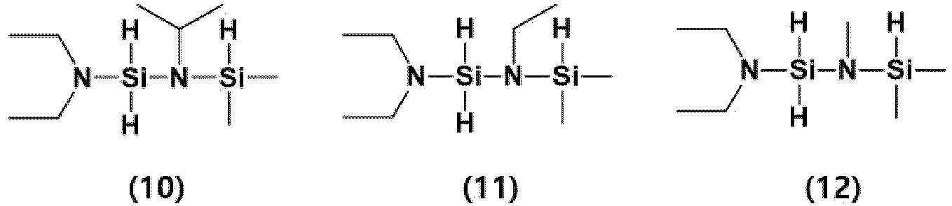
- The silicon precursor compound of claim 1, wherein the silicon precursor compound is selected from the following compounds (1) to (36):


- A method for preparing a silicon precursor compound, which comprises:a first step of reacting a chlorosilane derivative with a primary amine to form a first compound;a second step of reacting the first compound with an alkyl-lithium (Alkyl-Li) to form a second compound comprising lithium; anda third step of reacting the second compound with a silane compound to prepare a silicon precursor compound represented by the following Formula 1:
 in Formula 1, R0, R5, and R6 are each independently a linear or branched, saturated or unsaturated hydrocarbon group having 1 to 4 carbon atoms or an isomer thereof, R1, R2, R3, and R4 are each independently hydrogen (H), a halogen, or a linear or branched, saturated or unsaturated hydrocarbon group having 1 to 4 carbon atoms, and X is hydrogen (H) or a halogen.
 - The method for preparing a silicon precursor compound of claim 3, wherein the first compound is a compound represented by the following Formula 7:

- The method for preparing a silicon precursor compound of claim 3, wherein, when X and R1 in the silicon precursor compound represented by Formula 1 are each a halogen, the method comprises a fourth step of reacting it with a metal hydride.
- The method for preparing a silicon precursor compound of claim 3, wherein the silane compound is produced by reacting a chlorosilane derivative with a secondary amine.
- A method for preparing a silicon-containing thin film, which comprises forming a silicon-containing thin film using a silicon precursor compound represented by the following Formula 1:

- The method for preparing a silicon-containing thin film of claim 7, wherein the silicon precursor compound is selected from the following compounds (1) to (36):





- The method for preparing a silicon-containing thin film of claim 7, wherein the silicon-containing thin film is deposited by chemical vapor deposition (CVD) or atomic layer deposition (ALD).
- The method for preparing a silicon-containing thin film of claim 7, wherein the silicon-containing thin film is any one selected from the group consisting of a silicon oxide film (SiO2), a silicon oxycarbide film (SiOC), a silicon nitride film (SiN), a silicon oxynitride film (SiON), a silicon carbonitride film (SiCN), and a silicon carbonized film (SiC).
- The method for preparing a silicon-containing thin film of claim 9, wherein the silicon-containing thin film is a silicon oxide (SiO2) film, and the silicon oxide film is deposited by atomic layer deposition,
wherein the atomic layer deposition comprises providing a substrate to a reactor; introducing the silicon precursor compound into the reactor; purging the reactor with a purge gas; introducing an oxygen source into the reactor to react with the silicon precursor compound to form a silicon oxide film; and purging the reactor with the purge gas. - The method for preparing a silicon-containing thin film of claim 11, wherein the purge gas is selected from the group consisting of nitrogen, helium, argon, and mixtures thereof.
- The method for preparing a silicon-containing thin film of claim 11, wherein the oxygen source is selected from the group consisting of oxygen, peroxide, oxygen plasma, water vapor, water vapor plasma, hydrogen peroxide, ozone source, and mixtures thereof.
- The method for preparing a silicon-containing thin film of claim 11, wherein the oxygen source comprises plasma.
- The method for preparing a silicon-containing thin film of claim 14, wherein the plasma is generated in situ.
- The method for preparing a silicon-containing thin film of claim 11, wherein the atomic layer deposition is carried out at one or more temperatures of about 500°C or lower.
- The method for preparing a silicon-containing thin film of claim 9, wherein the silicon-containing thin film is a silicon nitride (SiN) film, and the silicon nitride film is deposited by plasma-enhanced atomic layer deposition,
wherein the plasma-enhanced atomic layer deposition comprises providing a substrate to a reactor; introducing the silicon precursor compound into the reactor; purging the reactor with a purge gas; introducing a nitrogen-containing plasma source and an inert gas into the reactor to react with the silicon precursor compound to form a silicon nitride film; and purging the reactor with a purge gas. - The method for preparing a silicon-containing thin film of claim 17, wherein the nitrogen-containing plasma source is selected from the group consisting of nitrogen plasma, nitrogen and argon mixed plasma, ammonia plasma, nitrogen and ammonia mixed plasma, ammonia and helium mixed plasma, ammonia and argon mixed plasma, ammonia and nitrogen mixed plasma, NF3 plasma, organic amine plasma, and mixtures thereof.
- The method for preparing a silicon-containing thin film of claim 17, wherein the method is carried out at one or more temperatures of about 400°C or lower.
Applications Claiming Priority (2)
| Application Number | Priority Date | Filing Date | Title |
|---|---|---|---|
| KR1020220050831A KR102723766B1 (en) | 2022-04-25 | 2022-04-25 | Silicon precursor compounds and method for manufacturing the same, and method of forming silicon-containing films |
| PCT/KR2023/005085 WO2023211027A1 (en) | 2022-04-25 | 2023-04-14 | Silicon precursor compound and preparation method therefor, and silicon-containing thin film preparation method using silicon precursor |
Publications (2)
| Publication Number | Publication Date |
|---|---|
| EP4516961A1 true EP4516961A1 (en) | 2025-03-05 |
| EP4516961A4 EP4516961A4 (en) | 2026-03-25 |
Family
ID=88519359
Family Applications (1)
| Application Number | Title | Priority Date | Filing Date |
|---|---|---|---|
| EP23796676.7A Pending EP4516961A4 (en) | 2022-04-25 | 2023-04-14 | SILICON PRECURSOR COMPOUND AND MANUFACTURING METHOD FOR IT, AS WELL AS SILICON-CONTAINING THIN-LAYER MANUFACTURING METHOD WITH THE SILICON PRECURSOR |
Country Status (7)
| Country | Link |
|---|---|
| US (1) | US20250051914A1 (en) |
| EP (1) | EP4516961A4 (en) |
| JP (1) | JP2025516176A (en) |
| KR (1) | KR102723766B1 (en) |
| CN (1) | CN119096005A (en) |
| TW (1) | TWI892120B (en) |
| WO (1) | WO2023211027A1 (en) |
Families Citing this family (1)
| Publication number | Priority date | Publication date | Assignee | Title |
|---|---|---|---|---|
| KR20250088352A (en) | 2023-12-08 | 2025-06-17 | (주)디엔에프 | Aminoalkoxydisilazane compounds, composition for depositing silicon-containing thin film containing the same and method of manufacturing silicon-containing thin film using the same |
Family Cites Families (8)
| Publication number | Priority date | Publication date | Assignee | Title |
|---|---|---|---|---|
| KR101444707B1 (en) | 2008-06-03 | 2014-09-26 | 에어 프로덕츠 앤드 케미칼스, 인코오포레이티드 | Low temperature deposition of silicon-containing films |
| US9969756B2 (en) * | 2014-09-23 | 2018-05-15 | L'Air Liquide, Société Anonyme pour l'Etude et l'Exploitation des Procédés George Claude | Carbosilane substituted amine precursors for deposition of Si-containing films and methods thereof |
| US9879340B2 (en) * | 2014-11-03 | 2018-01-30 | Versum Materials Us, Llc | Silicon-based films and methods of forming the same |
| US9929006B2 (en) * | 2016-07-20 | 2018-03-27 | Micron Technology, Inc. | Silicon chalcogenate precursors, methods of forming the silicon chalcogenate precursors, and related methods of forming silicon nitride and semiconductor structures |
| US10464953B2 (en) * | 2016-10-14 | 2019-11-05 | Versum Materials Us, Llc | Carbon bridged aminosilane compounds for high growth rate silicon-containing films |
| KR20180110612A (en) * | 2017-03-29 | 2018-10-10 | (주)디엔에프 | Compositions for depositing silicon-containing thin films containing bis(aminosilyl)alkylamine compound and methods for manufacturing silicon-containing thin film using the same |
| WO2020116386A1 (en) * | 2018-12-05 | 2020-06-11 | 住友精化株式会社 | Bis(alkylamino)disilazane compound, bis(alkylamino)disilazane compound-containing composition for forming silicon-containing film |
| EP3947769A4 (en) * | 2019-04-25 | 2023-01-11 | Versum Materials US, LLC | ORGANOAMINODISILAZANE FOR DEPOSIT BY ATOMIC LAYER AT HIGH TEMPERATURE OF THIN FILMS OF SILICON OXIDE |
-
2022
- 2022-04-25 KR KR1020220050831A patent/KR102723766B1/en active Active
-
2023
- 2023-04-14 WO PCT/KR2023/005085 patent/WO2023211027A1/en not_active Ceased
- 2023-04-14 JP JP2024563106A patent/JP2025516176A/en active Pending
- 2023-04-14 CN CN202380036294.0A patent/CN119096005A/en active Pending
- 2023-04-14 EP EP23796676.7A patent/EP4516961A4/en active Pending
- 2023-04-24 TW TW112115061A patent/TWI892120B/en active
-
2024
- 2024-10-25 US US18/927,285 patent/US20250051914A1/en active Pending
Also Published As
| Publication number | Publication date |
|---|---|
| WO2023211027A1 (en) | 2023-11-02 |
| KR20230151303A (en) | 2023-11-01 |
| TW202342489A (en) | 2023-11-01 |
| TWI892120B (en) | 2025-08-01 |
| US20250051914A1 (en) | 2025-02-13 |
| EP4516961A4 (en) | 2026-03-25 |
| CN119096005A (en) | 2024-12-06 |
| KR102723766B1 (en) | 2024-10-31 |
| JP2025516176A (en) | 2025-05-27 |
Similar Documents
| Publication | Publication Date | Title |
|---|---|---|
| JP7320544B2 (en) | Si-containing film-forming composition and method of use thereof | |
| CN103450242B (en) | Organoaminodisilane precursor and method for deposition of thin films comprising same | |
| TWI386414B (en) | Composition and method for low temperature chemical vapor deposition of germanium-containing film containing tantalum carbonitride and oxycarbonitride film | |
| TWI750577B (en) | Compositions and methods using same for silicon containing films | |
| JP6526562B2 (en) | Method for producing silicon-containing thin film | |
| WO2003046254A1 (en) | Method for the fabrication of silicon nitride, silicon oxynitride, and silicon oxide films by chemical vapor deposition | |
| US20250051914A1 (en) | Silicon precursor compound and preparation method therefor, and silicon-containing thin film preparation method using silicon precursor | |
| JP2009532395A (en) | PENTAKIS (DIMETHYLAMINO) DILANA PRECURSOR COMPOUND AND METHOD FOR PREPARING THE SAME | |
| JP2023542236A (en) | Composition for germanium seed layer and method of using it | |
| TWI852311B (en) | Halide-functionalized cyclotrisilazanes as precursors for deposition of silicon-containing films | |
| US20250230176A1 (en) | Silicon precursor compound in asymmetric structure, method for preparing the same, and method for preparing a silicon-containing thin film | |
| KR20250014292A (en) | Silicon precursor compounds and method for manufacturing the same, and method of forming silicon-containing films | |
| JP7065805B2 (en) | Halogenated aminosilane compounds, thin film forming compositions and silicon-containing thin films | |
| KR20230050655A (en) | Halogen-free tungsten compounds, preparation method thereof and process for the formation of thin films using the same | |
| KR20220166960A (en) | Fluorine-free tungsten compounds, preparation method thereof and process for the formation of thin films using the same |
Legal Events
| Date | Code | Title | Description |
|---|---|---|---|
| STAA | Information on the status of an ep patent application or granted ep patent |
Free format text: STATUS: THE INTERNATIONAL PUBLICATION HAS BEEN MADE |
|
| PUAI | Public reference made under article 153(3) epc to a published international application that has entered the european phase |
Free format text: ORIGINAL CODE: 0009012 |
|
| STAA | Information on the status of an ep patent application or granted ep patent |
Free format text: STATUS: REQUEST FOR EXAMINATION WAS MADE |
|
| 17P | Request for examination filed |
Effective date: 20241122 |
|
| AK | Designated contracting states |
Kind code of ref document: A1 Designated state(s): AL AT BE BG CH CY CZ DE DK EE ES FI FR GB GR HR HU IE IS IT LI LT LU LV MC ME MK MT NL NO PL PT RO RS SE SI SK SM TR |
|
| DAV | Request for validation of the european patent (deleted) | ||
| DAX | Request for extension of the european patent (deleted) | ||
| REG | Reference to a national code |
Ref country code: DE Ref legal event code: R079 Free format text: PREVIOUS MAIN CLASS: C23C0016340000 Ipc: C07F0007020000 |
|
| A4 | Supplementary search report drawn up and despatched |
Effective date: 20260219 |
|
| RIC1 | Information provided on ipc code assigned before grant |
Ipc: C07F 7/02 20060101AFI20260213BHEP Ipc: C23C 16/34 20060101ALI20260213BHEP Ipc: C23C 16/36 20060101ALI20260213BHEP Ipc: C23C 16/40 20060101ALI20260213BHEP Ipc: C23C 16/30 20060101ALI20260213BHEP Ipc: C23C 16/455 20060101ALI20260213BHEP Ipc: C23C 16/32 20060101ALI20260213BHEP Ipc: C07F 7/10 20060101ALI20260213BHEP Ipc: C07F 7/12 20060101ALI20260213BHEP |