EP4516763A1 - Vacuum wafer chuck with solid diamond pins - Google Patents
Vacuum wafer chuck with solid diamond pins Download PDFInfo
- Publication number
- EP4516763A1 EP4516763A1 EP24161127.6A EP24161127A EP4516763A1 EP 4516763 A1 EP4516763 A1 EP 4516763A1 EP 24161127 A EP24161127 A EP 24161127A EP 4516763 A1 EP4516763 A1 EP 4516763A1
- Authority
- EP
- European Patent Office
- Prior art keywords
- main body
- reaction
- body portion
- pins
- silicon carbide
- Prior art date
- Legal status (The legal status is an assumption and is not a legal conclusion. Google has not performed a legal analysis and makes no representation as to the accuracy of the status listed.)
- Pending
Links
Images


Classifications
-
- C—CHEMISTRY; METALLURGY
- C04—CEMENTS; CONCRETE; ARTIFICIAL STONE; CERAMICS; REFRACTORIES
- C04B—LIME, MAGNESIA; SLAG; CEMENTS; COMPOSITIONS THEREOF, e.g. MORTARS, CONCRETE OR LIKE BUILDING MATERIALS; ARTIFICIAL STONE; CERAMICS; REFRACTORIES; TREATMENT OF NATURAL STONE
- C04B35/00—Shaped ceramic products characterised by their composition; Ceramics compositions; Processing powders of inorganic compounds preparatory to the manufacturing of ceramic products
- C04B35/71—Ceramic products containing macroscopic reinforcing agents
- C04B35/78—Ceramic products containing macroscopic reinforcing agents containing non-metallic materials
- C04B35/80—Fibres, filaments, whiskers, platelets, or the like
-
- H—ELECTRICITY
- H10—SEMICONDUCTOR DEVICES; ELECTRIC SOLID-STATE DEVICES NOT OTHERWISE PROVIDED FOR
- H10P—GENERIC PROCESSES OR APPARATUS FOR THE MANUFACTURE OR TREATMENT OF DEVICES COVERED BY CLASS H10
- H10P72/00—Handling or holding of wafers, substrates or devices during manufacture or treatment thereof
- H10P72/70—Handling or holding of wafers, substrates or devices during manufacture or treatment thereof for supporting or gripping
- H10P72/78—Handling or holding of wafers, substrates or devices during manufacture or treatment thereof for supporting or gripping using vacuum or suction, e.g. Bernoulli chucks
-
- H—ELECTRICITY
- H10—SEMICONDUCTOR DEVICES; ELECTRIC SOLID-STATE DEVICES NOT OTHERWISE PROVIDED FOR
- H10P—GENERIC PROCESSES OR APPARATUS FOR THE MANUFACTURE OR TREATMENT OF DEVICES COVERED BY CLASS H10
- H10P72/00—Handling or holding of wafers, substrates or devices during manufacture or treatment thereof
- H10P72/70—Handling or holding of wafers, substrates or devices during manufacture or treatment thereof for supporting or gripping
- H10P72/76—Handling or holding of wafers, substrates or devices during manufacture or treatment thereof for supporting or gripping using mechanical means, e.g. clamps or pinches
- H10P72/7604—Handling or holding of wafers, substrates or devices during manufacture or treatment thereof for supporting or gripping using mechanical means, e.g. clamps or pinches the wafers being placed on a susceptor, stage or support
- H10P72/7616—Handling or holding of wafers, substrates or devices during manufacture or treatment thereof for supporting or gripping using mechanical means, e.g. clamps or pinches the wafers being placed on a susceptor, stage or support characterised by a coating, a hardness or a material
-
- C—CHEMISTRY; METALLURGY
- C04—CEMENTS; CONCRETE; ARTIFICIAL STONE; CERAMICS; REFRACTORIES
- C04B—LIME, MAGNESIA; SLAG; CEMENTS; COMPOSITIONS THEREOF, e.g. MORTARS, CONCRETE OR LIKE BUILDING MATERIALS; ARTIFICIAL STONE; CERAMICS; REFRACTORIES; TREATMENT OF NATURAL STONE
- C04B35/00—Shaped ceramic products characterised by their composition; Ceramics compositions; Processing powders of inorganic compounds preparatory to the manufacturing of ceramic products
- C04B35/515—Shaped ceramic products characterised by their composition; Ceramics compositions; Processing powders of inorganic compounds preparatory to the manufacturing of ceramic products based on non-oxide ceramics
- C04B35/52—Shaped ceramic products characterised by their composition; Ceramics compositions; Processing powders of inorganic compounds preparatory to the manufacturing of ceramic products based on non-oxide ceramics based on carbon, e.g. graphite
-
- C—CHEMISTRY; METALLURGY
- C04—CEMENTS; CONCRETE; ARTIFICIAL STONE; CERAMICS; REFRACTORIES
- C04B—LIME, MAGNESIA; SLAG; CEMENTS; COMPOSITIONS THEREOF, e.g. MORTARS, CONCRETE OR LIKE BUILDING MATERIALS; ARTIFICIAL STONE; CERAMICS; REFRACTORIES; TREATMENT OF NATURAL STONE
- C04B35/00—Shaped ceramic products characterised by their composition; Ceramics compositions; Processing powders of inorganic compounds preparatory to the manufacturing of ceramic products
- C04B35/515—Shaped ceramic products characterised by their composition; Ceramics compositions; Processing powders of inorganic compounds preparatory to the manufacturing of ceramic products based on non-oxide ceramics
- C04B35/56—Shaped ceramic products characterised by their composition; Ceramics compositions; Processing powders of inorganic compounds preparatory to the manufacturing of ceramic products based on non-oxide ceramics based on carbides or oxycarbides
- C04B35/565—Shaped ceramic products characterised by their composition; Ceramics compositions; Processing powders of inorganic compounds preparatory to the manufacturing of ceramic products based on non-oxide ceramics based on carbides or oxycarbides based on silicon carbide
-
- C—CHEMISTRY; METALLURGY
- C04—CEMENTS; CONCRETE; ARTIFICIAL STONE; CERAMICS; REFRACTORIES
- C04B—LIME, MAGNESIA; SLAG; CEMENTS; COMPOSITIONS THEREOF, e.g. MORTARS, CONCRETE OR LIKE BUILDING MATERIALS; ARTIFICIAL STONE; CERAMICS; REFRACTORIES; TREATMENT OF NATURAL STONE
- C04B35/00—Shaped ceramic products characterised by their composition; Ceramics compositions; Processing powders of inorganic compounds preparatory to the manufacturing of ceramic products
- C04B35/515—Shaped ceramic products characterised by their composition; Ceramics compositions; Processing powders of inorganic compounds preparatory to the manufacturing of ceramic products based on non-oxide ceramics
- C04B35/56—Shaped ceramic products characterised by their composition; Ceramics compositions; Processing powders of inorganic compounds preparatory to the manufacturing of ceramic products based on non-oxide ceramics based on carbides or oxycarbides
- C04B35/565—Shaped ceramic products characterised by their composition; Ceramics compositions; Processing powders of inorganic compounds preparatory to the manufacturing of ceramic products based on non-oxide ceramics based on carbides or oxycarbides based on silicon carbide
- C04B35/573—Shaped ceramic products characterised by their composition; Ceramics compositions; Processing powders of inorganic compounds preparatory to the manufacturing of ceramic products based on non-oxide ceramics based on carbides or oxycarbides based on silicon carbide obtained by reaction sintering or recrystallisation
-
- C—CHEMISTRY; METALLURGY
- C04—CEMENTS; CONCRETE; ARTIFICIAL STONE; CERAMICS; REFRACTORIES
- C04B—LIME, MAGNESIA; SLAG; CEMENTS; COMPOSITIONS THEREOF, e.g. MORTARS, CONCRETE OR LIKE BUILDING MATERIALS; ARTIFICIAL STONE; CERAMICS; REFRACTORIES; TREATMENT OF NATURAL STONE
- C04B37/00—Joining burned ceramic articles with other burned ceramic articles or other articles by heating
- C04B37/003—Joining burned ceramic articles with other burned ceramic articles or other articles by heating by means of an interlayer consisting of a combination of materials selected from glass, or ceramic material with metals, metal oxides or metal salts
- C04B37/005—Joining burned ceramic articles with other burned ceramic articles or other articles by heating by means of an interlayer consisting of a combination of materials selected from glass, or ceramic material with metals, metal oxides or metal salts consisting of glass or ceramic material
-
- H—ELECTRICITY
- H10—SEMICONDUCTOR DEVICES; ELECTRIC SOLID-STATE DEVICES NOT OTHERWISE PROVIDED FOR
- H10P—GENERIC PROCESSES OR APPARATUS FOR THE MANUFACTURE OR TREATMENT OF DEVICES COVERED BY CLASS H10
- H10P72/00—Handling or holding of wafers, substrates or devices during manufacture or treatment thereof
- H10P72/70—Handling or holding of wafers, substrates or devices during manufacture or treatment thereof for supporting or gripping
- H10P72/76—Handling or holding of wafers, substrates or devices during manufacture or treatment thereof for supporting or gripping using mechanical means, e.g. clamps or pinches
- H10P72/7604—Handling or holding of wafers, substrates or devices during manufacture or treatment thereof for supporting or gripping using mechanical means, e.g. clamps or pinches the wafers being placed on a susceptor, stage or support
- H10P72/7614—Handling or holding of wafers, substrates or devices during manufacture or treatment thereof for supporting or gripping using mechanical means, e.g. clamps or pinches the wafers being placed on a susceptor, stage or support characterised by a plurality of individual support members, e.g. support posts or protrusions
-
- H—ELECTRICITY
- H10—SEMICONDUCTOR DEVICES; ELECTRIC SOLID-STATE DEVICES NOT OTHERWISE PROVIDED FOR
- H10P—GENERIC PROCESSES OR APPARATUS FOR THE MANUFACTURE OR TREATMENT OF DEVICES COVERED BY CLASS H10
- H10P72/00—Handling or holding of wafers, substrates or devices during manufacture or treatment thereof
- H10P72/70—Handling or holding of wafers, substrates or devices during manufacture or treatment thereof for supporting or gripping
- H10P72/76—Handling or holding of wafers, substrates or devices during manufacture or treatment thereof for supporting or gripping using mechanical means, e.g. clamps or pinches
- H10P72/7604—Handling or holding of wafers, substrates or devices during manufacture or treatment thereof for supporting or gripping using mechanical means, e.g. clamps or pinches the wafers being placed on a susceptor, stage or support
- H10P72/7624—Handling or holding of wafers, substrates or devices during manufacture or treatment thereof for supporting or gripping using mechanical means, e.g. clamps or pinches the wafers being placed on a susceptor, stage or support characterised by the mechanical construction of the susceptor, stage or support
-
- C—CHEMISTRY; METALLURGY
- C04—CEMENTS; CONCRETE; ARTIFICIAL STONE; CERAMICS; REFRACTORIES
- C04B—LIME, MAGNESIA; SLAG; CEMENTS; COMPOSITIONS THEREOF, e.g. MORTARS, CONCRETE OR LIKE BUILDING MATERIALS; ARTIFICIAL STONE; CERAMICS; REFRACTORIES; TREATMENT OF NATURAL STONE
- C04B2235/00—Aspects relating to ceramic starting mixtures or sintered ceramic products
- C04B2235/02—Composition of constituents of the starting material or of secondary phases of the final product
- C04B2235/30—Constituents and secondary phases not being of a fibrous nature
- C04B2235/38—Non-oxide ceramic constituents or additives
- C04B2235/3817—Carbides
- C04B2235/3826—Silicon carbides
-
- C—CHEMISTRY; METALLURGY
- C04—CEMENTS; CONCRETE; ARTIFICIAL STONE; CERAMICS; REFRACTORIES
- C04B—LIME, MAGNESIA; SLAG; CEMENTS; COMPOSITIONS THEREOF, e.g. MORTARS, CONCRETE OR LIKE BUILDING MATERIALS; ARTIFICIAL STONE; CERAMICS; REFRACTORIES; TREATMENT OF NATURAL STONE
- C04B2235/00—Aspects relating to ceramic starting mixtures or sintered ceramic products
- C04B2235/02—Composition of constituents of the starting material or of secondary phases of the final product
- C04B2235/30—Constituents and secondary phases not being of a fibrous nature
- C04B2235/42—Non metallic elements added as constituents or additives, e.g. sulfur, phosphor, selenium or tellurium
- C04B2235/422—Carbon
- C04B2235/427—Diamond
-
- C—CHEMISTRY; METALLURGY
- C04—CEMENTS; CONCRETE; ARTIFICIAL STONE; CERAMICS; REFRACTORIES
- C04B—LIME, MAGNESIA; SLAG; CEMENTS; COMPOSITIONS THEREOF, e.g. MORTARS, CONCRETE OR LIKE BUILDING MATERIALS; ARTIFICIAL STONE; CERAMICS; REFRACTORIES; TREATMENT OF NATURAL STONE
- C04B2235/00—Aspects relating to ceramic starting mixtures or sintered ceramic products
- C04B2235/60—Aspects relating to the preparation, properties or mechanical treatment of green bodies or pre-forms
- C04B2235/614—Gas infiltration of green bodies or pre-forms
-
- C—CHEMISTRY; METALLURGY
- C04—CEMENTS; CONCRETE; ARTIFICIAL STONE; CERAMICS; REFRACTORIES
- C04B—LIME, MAGNESIA; SLAG; CEMENTS; COMPOSITIONS THEREOF, e.g. MORTARS, CONCRETE OR LIKE BUILDING MATERIALS; ARTIFICIAL STONE; CERAMICS; REFRACTORIES; TREATMENT OF NATURAL STONE
- C04B2237/00—Aspects relating to ceramic laminates or to joining of ceramic articles with other articles by heating
- C04B2237/30—Composition of layers of ceramic laminates or of ceramic or metallic articles to be joined by heating, e.g. Si substrates
- C04B2237/32—Ceramic
- C04B2237/36—Non-oxidic
- C04B2237/363—Carbon
-
- C—CHEMISTRY; METALLURGY
- C04—CEMENTS; CONCRETE; ARTIFICIAL STONE; CERAMICS; REFRACTORIES
- C04B—LIME, MAGNESIA; SLAG; CEMENTS; COMPOSITIONS THEREOF, e.g. MORTARS, CONCRETE OR LIKE BUILDING MATERIALS; ARTIFICIAL STONE; CERAMICS; REFRACTORIES; TREATMENT OF NATURAL STONE
- C04B2237/00—Aspects relating to ceramic laminates or to joining of ceramic articles with other articles by heating
- C04B2237/30—Composition of layers of ceramic laminates or of ceramic or metallic articles to be joined by heating, e.g. Si substrates
- C04B2237/32—Ceramic
- C04B2237/36—Non-oxidic
- C04B2237/365—Silicon carbide
-
- C—CHEMISTRY; METALLURGY
- C04—CEMENTS; CONCRETE; ARTIFICIAL STONE; CERAMICS; REFRACTORIES
- C04B—LIME, MAGNESIA; SLAG; CEMENTS; COMPOSITIONS THEREOF, e.g. MORTARS, CONCRETE OR LIKE BUILDING MATERIALS; ARTIFICIAL STONE; CERAMICS; REFRACTORIES; TREATMENT OF NATURAL STONE
- C04B2237/00—Aspects relating to ceramic laminates or to joining of ceramic articles with other articles by heating
- C04B2237/50—Processing aspects relating to ceramic laminates or to the joining of ceramic articles with other articles by heating
- C04B2237/61—Joining two substrates of which at least one is porous by infiltrating the porous substrate with a liquid, such as a molten metal, causing bonding of the two substrates, e.g. joining two porous carbon substrates by infiltrating with molten silicon
Definitions
- the present disclosure generally relates to a vacuum wafer chuck with solid diamond pins.
- aspects of the present disclosure relate to a vacuum wafer chuck with solid diamond pins.
- Various issues may exist with conventional solutions for a vacuum wafer chuck with solid diamond pins.
- conventional systems and methods for a vacuum wafer chuck with solid diamond pins may be costly, cumbersome, and/or inefficient.
- x or y means any element of the three-element set ⁇ (x), (y), (x, y) ⁇ .
- x, y, or z means any element of the seven-element set ⁇ (x), (y), (z), (x, y), (x, z), (y, z), (x, y, z) ⁇ .
- first means “first,” “second,” etc. may be used herein to describe various elements, and these elements should not be limited by these terms. These terms are only used to distinguish one element from another. Thus, for example, a first element discussed in this disclosure could be termed a second element without departing from the teachings of the present disclosure.
- Coupled may be used to describe two elements directly contacting each other or describe two elements indirectly connected by one or more other elements.
- element A is coupled to element B, then element A can be directly contacting element B or indirectly connected to element B by an intervening element C.
- the terms “over” or “on” may be used to describe two elements directly contacting each other or describe two elements indirectly connected by one or more other elements.
- the reaction-bonded silicon carbide body 100 may include a main body portion 110.
- the reaction-bonded silicon carbide body 100 may also include one or more discrete elements 120 of a dimension, located at least partially within the main body portion 110.
- the main body portion 110 may include reaction-bonded silicon carbide 112 and elemental silicon 114 without comprising diamond.
- the one or more discrete elements 120 may also include a single diamond particle 122 of the dimension.
- Reaction-bonded silicon carbide 112 may surround the diamond particles 122, and elemental silicon 114.
- the main body portion 110 may be configured for use within a vacuum wafer chuck.
- the discrete elements 120 may be configured to provide high heat flux directly under a die, without reducing the machinability of the main body portion 110.
- the discrete elements 120 may be configured to provide local diamond reinforcement at a wear face, without reducing the machinability of the main body portion 110.
- FIG. 3a to FIG. 3d are cross-sectional views of a reaction-bonded ceramic material 20 which includes ceramic particles 22, reaction-formed silicon carbide (SiC) particles 24, and residual elemental silicon (Si) 26.
- the ceramic particles 22 may include SiC or boron carbide (B4C).
- the ceramic material 20 may be produced by performing a reactive infiltration process on a preform 30 ( FIG. 3b ) which comprises the ceramic particles 22 and elemental carbon 32. During the infiltration process, molten Si may infiltrate the preform 30 to form the reaction-formed SiC particles 24. That is, the molten Si may react with the carbon 32 to form additional SiC.
- FIG. 3a is a cross-sectional view of a reaction-bonded ceramic material 40 which comprises reaction-formed SiC particles 24, residual elemental Si 26, diamond particles 42, reaction-formed SiC coatings 44 located on and surrounding the diamond particles 42, and, optionally, ceramic particles 22.
- the ceramic particles 22, if desired, may include SiC or B4C.
- the ceramic material 40 may be produced by performing a reactive-infiltration process on a preform 50 ( FIG.
- molten Si infiltrates the preform 50 to form the reaction-formed SiC particles 24 and the reaction-formed SiC coatings 44. If desired, the coatings 44 may completely surround the diamond particles 42 such that the coatings 44 appear as halos surrounding the particles 42 in the cross-sectional view of FIG. 3c .
- the molten Si reacts with the carbon 32 to form additional SiC, and the molten Si also reacts with surfaces of the diamond particles 42 to produce the reaction-formed SiC coatings 44.
- the process may result in only a small increase in volume (the increase in volume of the ceramic material 40 compared to that of the preform 50) that may be less than one percent.
- the material 40 illustrated in FIG. 3c which comprises a composite of reaction bonded SiC 24, 44, diamond particles 42 (SiSiC-diamond), may be considered for many high-end applications, because the material 40 may have low thermal expansion, high thermal conductivity, high hardness, high wear resistance, high stiffness, and low coefficient of friction.
- the diamond particles 42 may make the material 40 extremely difficult to machine (cut, grind, and/or shape).
- discrete reinforcement elements may be provided for a reaction-bonded SiC body, where the reinforcement elements include the diamond particles 42 while the body, for example main body portion 110, does not contain diamond.
- the diamond-containing material 40 illustrated in FIG. 3c may be located only where needed to provide desired performance.
- the remainder of the body may be formed of the material 20 illustrated in FIG.3a , which contains reaction-bonded SiC 24 but no diamond, and which is well suited to cost-effective machining.
- Diamond has many desirable characteristics for a variety of useful applications. Such characteristics include extremely high hardness for wear resistance, very low coefficient of friction for sliding applications, very high stiffness (Young's modulus) for structural applications, and extreme thermal stability (high thermal conductivity and low coefficient of thermal expansion (CTE)).
- desirable diamond particles may be single crystals and/or polycrystalline crystals. Often, polycrystalline diamond particles may exhibit more uniform properties, e.g. hardness, in different physical directions/planes of the crystal particle.
- FIG. 4a is a top view of an example of a multi-component block.
- the illustrated block includes a body 110 (an example of a main body portion 110) formed of the SiC containing material 20 illustrated in FIG. 3a , and discrete, spaced-apart features 104 formed of the diamond-containing material illustrated in FIG. 3c .
- the features 104 may be located in corresponding trenches 106 (examples of surface features, FIG. 4b ) that are laser machined into the top surface 108 of the SiC-containing body 102.
- each feature 104 may have a width W in a range of from 0.5 mm to 3.0 mm, preferably about 1.2 mm, and a depth D in a range of from 100 ⁇ m to 600 ⁇ m, preferably about 300 ⁇ m, and the trenches 106 may be at least partially filled with a suitable amount, such as nominally 65 ⁇ m, of diamond powder.
- a suitable amount such as nominally 65 ⁇ m, of diamond powder.
- the multi-component block can use the discrete features 104 to provide the high-performance characteristics associated with the diamond-containing material 40 only where desired, while the remainder of the block 100 (that is, the body 110) contains reaction-formed SiC but no diamond and therefore may be more easily machined.
- the reactions that occur in the trenches 106, which involve Si + diamond, are different from the reactions that occur simultaneously elsewhere in the body 110, which involve Si + carbon but no diamond.
- the residual elemental Si content in the diamond-reinforced region (within the trenches 106) is lower than in the rest of the block.
- the residual elemental Si in the diamond-reinforced region within the trenches 106 may be about 6.8%, for example, while the residual Si in the SiSiC (and no diamond) region may be about 23.2%, for example.
- the lower residual Si content in the diamond-reinforced region may yield improved properties (hardness, stiffness, inertness, etc.), but the combination of diamond particles and low elemental Si content may make machining especially difficult, such that it may be especially advantageous to locate the diamond-containing features 104 only where needed.
- avoiding difficult machining is only one of many reasons why localizing diamond-containing features may be advantageous.
- Another advantage of providing diamond reinforcement only where it can be put to effective use is reduced cost. In other words, it is advantageous to use high-cost diamond powder only where it is needed.
- FIG. 5 illustrates an exemplary reaction-bonded silicon carbide body 100 using a single diamond particle 122 for a discrete element 120, before machining.
- a reaction-bonded silicon carbide body 100 comprising a main body portion 110, wherein the main body portion 110 comprises a single diamond particle 122, reaction-bonded silicon carbide 112, and elemental silicon 114.
- the main body portion 110 does not contain diamond other than the diamond particle 122.
- the main body portion 110 does not comprise diamond other than particle 122.
- the diamond particle 122 may be of a significantly larger dimension than diamond particles used in powder form as illustrated in FIG. 4a to 4c .
- the diamond particle 122 may have a dimension of 600 ⁇ m, for example. The diamond particle 122 may thus be embedded in the main body portion 110.
- FIG. 6 illustrates a cross-section and a top view of a reaction-bonded silicon carbide body 100, after machining.
- a reaction-bonded silicon carbide body 100 a main body portion 110.
- discrete elements 120 comprising pins 216.
- the pins 216 may be formed from a single diamond particle 122 through machining.
- the pins 216 comprise a first portion 217 located in the main body portion 110 and a second portion 218 that may stand proud of the surface of the main body portion 110.
- the pins 216 may comprise a top surface 212.
- the pins 216 may be, for example, of a conical frustrum shape with a first base diameter 220 and a second smaller diameter 222.
- the pins 216 may be any suitable shape, for example triangular or square or pentagonal frustrums.
- the frustrums may, in some embodiments, approach or even become substantially cylindrical.
- the shape of the pins 216 may comprise multiple stacked frustrums, or the shape may be approximated by an arbitrary number of stacked frustrums.
- the diameter of the pins 216 due to the often slightly conical shape, may be of a nominal dimension, that may be considered equal to the first diameter 220, the second diameter 222, or somewhere between the first diameter 220 and the second diameter 222, for example.
- a structure, for example pin 216, as shown in FIG. 6 may be machined from a single diamond particle 122 embedded in a main body portion 110 ( FIG. 5 ), comprising reaction bonded silicon carbide 112 and elemental silicon 114, for example.
- the machining may comprise simple surface grinding to produce a common top surface, that may produce flat top surfaces 212 of the pins 216 later. More of the main body portion 110 may then be machined away, to form the pins 216 and to make them stand proud above the top surface of the main body portion 110. Suitable machining may be laser cutting.
- the pins 216 may therefore be discrete elements of a dimension, a diameter, that may be partly located within the main body portion 110.
- the diameters of the diamond containing pins 216 may be, for example, in the range of from 200 ⁇ m to 800 ⁇ m, preferably about 400 ⁇ m.
- the heights of the pins 216 may likewise be in the range of from 200 ⁇ m to 800 ⁇ m, preferably about 400 ⁇ m, but these are just examples of how the present disclosure may be implemented. The present disclosure should not be limited to the details of the examples described herein.
- FIG. 7 is a flowchart that describes a method, according to some embodiments of the present disclosure.
- the method may comprise embedding a single diamond particle 122 of a pre-cut dimension into a main body portion 110 (see also FIG. 5 ).
- the method may comprise cutting one or more discrete elements 120 of a dimension, each of the dimension smaller than the pre-cut dimension, and each discrete element 120 located at least partially within the main body portion 110.
- the main body portion 110 may comprise reaction-bonded silicon carbide 112, elemental silicon 114, and does not comprise diamond outside of the discrete elements, e.g., particles 122.
- Each of the discrete elements 120, e.g., pins 216 may comprise a single diamond particle 122 of a post-cut dimension.
- the method may comprise cutting one or more discrete elements 120 of a dimension, each of the dimensions smaller than the pre-cut dimensions, and each of the discrete elements 120 located at least partially within the main body portion 110, and wherein each of the discrete elements 120 comprises a single diamond particle 122 of the dimension.
- the method may include configuring the main body portion 110 for use within a vacuum wafer chuck.
- the method may include configuring the discrete elements 120, e.g., pins 216, to provide high heat flux directly under a die, without reducing the machinability of the main body portion 110.
- the method may include configuring the discrete elements 120 to provide local diamond reinforcement at a wear face (e.g., top surface 212), without reducing the machinability of the main body portion 110.
- the method may include cutting the discrete elements 120 to form pins 216 for supporting a semiconductor wafer.
- the method may include forming the pins 216 to comprise a first portion 217 located within the main body portion 110, and the pins 216 to stand proud above the main body portion 110.
- the pins may, as in FIG. 6 , comprise a first portion 217 with a first diameter 220 and a second portion 218 with a second diameter 222.
- the first diameter may be greater or equal than the second diameter, the second diameter being substantially equal to the dimension, for example.
- the method may include forming the pins such that they may be separated from each other to prevent bi-metallic strip stresses.
- Implementations as described herein may relate to the following: A vacuum wafer chuck with solid diamond pins.
- the VCSEL device may comprise a plurality of layers forming a protective diode outside of the lithographic aperture area, wherein the surface area of the protective diode is larger than the surface area of said lithographic aperture.
Landscapes
- Chemical & Material Sciences (AREA)
- Engineering & Computer Science (AREA)
- Ceramic Engineering (AREA)
- Organic Chemistry (AREA)
- Materials Engineering (AREA)
- Structural Engineering (AREA)
- Manufacturing & Machinery (AREA)
- Chemical Kinetics & Catalysis (AREA)
- Container, Conveyance, Adherence, Positioning, Of Wafer (AREA)
- Physics & Mathematics (AREA)
- Optics & Photonics (AREA)
- Plasma & Fusion (AREA)
- Mechanical Engineering (AREA)
- Ceramic Products (AREA)
Abstract
A vacuum wafer chuck with solid diamond pins. The VCSEL device may comprise a plurality of layers forming a protective diode outside of the lithographic aperture area, wherein the surface area of the protective diode is larger than the surface area of said lithographic aperture.
Description
- The present disclosure generally relates to a vacuum wafer chuck with solid diamond pins.
- Aspects of the present disclosure relate to a vacuum wafer chuck with solid diamond pins. Various issues may exist with conventional solutions for a vacuum wafer chuck with solid diamond pins. In this regard, conventional systems and methods for a vacuum wafer chuck with solid diamond pins may be costly, cumbersome, and/or inefficient.
- Limitations and disadvantages of conventional systems and methods will become apparent to one of skill in the art, through comparison of such approaches with some aspects of the present methods and systems set forth in the remainder of this disclosure with reference to the drawings.
- Shown in and/or described in connection with at least one of the figures, and set forth more completely in the claims are a vacuum wafer chuck with solid diamond pins.
- These and other advantages, aspects and novel features of the present disclosure, as well as details of illustrated embodiments thereof, will be more fully understood from the following description and drawings.
- The various features and advantages of the present disclosure may be more readily understood with reference to the following detailed description taken in conjunction with the accompanying drawings, wherein like reference numerals designate like structural elements.
-
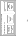
FIG. 1 is a block diagram illustrating a reaction-bonded silicon carbide body, according to some embodiments of the present disclosure. -
FIG. 2 is a block diagram that further describes the reaction-bondedsilicon carbide body 100 fromFIG. 1 . -
FIG. 3a to FIG. 3d are cross-sectional views of a reaction-bondedceramic material 20. -
FIG. 4a is a top view of an example of a multi-component block. -
FIG. 4b and 4c illustrate exemplary details ofFIG. 4a . -
FIG. 5 illustrates an exemplary reaction-bondedsilicon carbide body 100 using asingle diamond particle 122 for adiscrete element 120, before machining. -
FIG. 6 illustrates a cross-section and a top view of a reaction-bonded silicon carbide body, after machining. -
FIG. 7 is a flowchart that describes a method, according to some embodiments of the present disclosure. - The following discussion provides various examples of semiconductor devices and methods of manufacturing semiconductor devices. Such examples are non-limiting, and the scope of the appended claims should not be limited to the particular examples disclosed. In the following discussion, the terms "example" and "e.g." are non-limiting.
- The figures illustrate the general manner of construction, and descriptions and details of well-known features and techniques may be omitted to avoid unnecessarily obscuring the present disclosure. In addition, elements in the drawing figures are not necessarily drawn to scale. For example, the dimensions of some of the elements in the figures may be exaggerated relative to other elements to help improve understanding of the examples discussed in the present disclosure. The same reference numerals in different figures denote the same elements.
- The term "or" means any one or more of the items in the list joined by "or". As an example, "x or y" means any element of the three-element set {(x), (y), (x, y)}. As another example, "x, y, or z" means any element of the seven-element set {(x), (y), (z), (x, y), (x, z), (y, z), (x, y, z)}.
- The terms "comprises," "comprising," "includes," and/or "including," are "open ended" terms and specify the presence of stated features, but do not preclude the presence or addition of one or more other features.
- The terms "first," "second," etc. may be used herein to describe various elements, and these elements should not be limited by these terms. These terms are only used to distinguish one element from another. Thus, for example, a first element discussed in this disclosure could be termed a second element without departing from the teachings of the present disclosure.
- Unless specified otherwise, the term "coupled" may be used to describe two elements directly contacting each other or describe two elements indirectly connected by one or more other elements. For example, if element A is coupled to element B, then element A can be directly contacting element B or indirectly connected to element B by an intervening element C. Similarly, the terms "over" or "on" may be used to describe two elements directly contacting each other or describe two elements indirectly connected by one or more other elements.
- Referring now to
FIG. 1 , there is shown a block diagram that describes a reaction-bondedsilicon carbide body 100, according to some embodiments of the present disclosure. In some embodiments, the reaction-bondedsilicon carbide body 100 may include amain body portion 110. The reaction-bondedsilicon carbide body 100 may also include one or morediscrete elements 120 of a dimension, located at least partially within themain body portion 110. Themain body portion 110 may include reaction-bondedsilicon carbide 112 andelemental silicon 114 without comprising diamond. The one or morediscrete elements 120 may also include asingle diamond particle 122 of the dimension. Reaction-bondedsilicon carbide 112 may surround thediamond particles 122, andelemental silicon 114. - In some embodiments, the
main body portion 110 may be configured for use within a vacuum wafer chuck. In some embodiments, thediscrete elements 120 may be configured to provide high heat flux directly under a die, without reducing the machinability of themain body portion 110. In some embodiments, thediscrete elements 120 may be configured to provide local diamond reinforcement at a wear face, without reducing the machinability of themain body portion 110. -
FIG. 2 is a block diagram that further describes the reaction-bondedsilicon carbide body 100 fromFIG. 1 , according to some embodiments of the present disclosure. In some embodiments, the one or morediscrete elements 120 may includepins 216 for supporting a semiconductor wafer, for example. In some embodiments, thepins 216 may includefirst portions 217 located within themain body portion 110 andsecond portions 218 which stand proud above themain body portion 110 and thefirst portions 217. In some embodiments, thefirst portions 217 of thepins 216 may comprise afirst diameter 220. Thesecond portions 218 may comprise asecond diameter 222. Thefirst diameter 220 may be smaller than thesecond diameter 222, the second (or first)diameter 222 being substantially equal to the dimension. -
FIG. 3a to FIG. 3d are cross-sectional views of a reaction-bondedceramic material 20 which includesceramic particles 22, reaction-formed silicon carbide (SiC)particles 24, and residual elemental silicon (Si) 26. Theceramic particles 22 may include SiC or boron carbide (B4C). Theceramic material 20 may be produced by performing a reactive infiltration process on a preform 30 (FIG. 3b ) which comprises theceramic particles 22 andelemental carbon 32. During the infiltration process, molten Si may infiltrate thepreform 30 to form the reaction-formedSiC particles 24. That is, the molten Si may react with thecarbon 32 to form additional SiC. Despite the infiltration of Si into thepreform 30, the process may result in only a small increase in volume (the increase in volume of theceramic material 20 compared to that of the preform 30) that may be less than one percent, for example. Theceramic material 20 illustrated inFIG. 3a does not contain diamond.FIG. 3c is a cross-sectional view of a reaction-bondedceramic material 40 which comprises reaction-formedSiC particles 24, residualelemental Si 26,diamond particles 42, reaction-formedSiC coatings 44 located on and surrounding thediamond particles 42, and, optionally,ceramic particles 22. Theceramic particles 22, if desired, may include SiC or B4C. Theceramic material 40 may be produced by performing a reactive-infiltration process on a preform 50 (FIG. 3d ) which may include powder, and which includes the optionalceramic particles 22,elemental carbon 32, and thediamond particles 42. During the reactive-infiltration process, molten Si infiltrates thepreform 50 to form the reaction-formedSiC particles 24 and the reaction-formedSiC coatings 44. If desired, thecoatings 44 may completely surround thediamond particles 42 such that thecoatings 44 appear as halos surrounding theparticles 42 in the cross-sectional view ofFIG. 3c . During the reactive-infiltration process, the molten Si reacts with thecarbon 32 to form additional SiC, and the molten Si also reacts with surfaces of thediamond particles 42 to produce the reaction-formedSiC coatings 44. Despite the infiltration of the molten Si into thepreform 50, the process may result in only a small increase in volume (the increase in volume of theceramic material 40 compared to that of the preform 50) that may be less than one percent. - The material 40 illustrated in
FIG. 3c , which comprises a composite of reaction bondedSiC material 40 may have low thermal expansion, high thermal conductivity, high hardness, high wear resistance, high stiffness, and low coefficient of friction. However, thediamond particles 42 may make the material 40 extremely difficult to machine (cut, grind, and/or shape). Thus, according to the present disclosure, discrete reinforcement elements may be provided for a reaction-bonded SiC body, where the reinforcement elements include thediamond particles 42 while the body, for examplemain body portion 110, does not contain diamond. According to the present disclosure, the diamond-containingmaterial 40 illustrated inFIG. 3c may be located only where needed to provide desired performance. The remainder of the body may be formed of the material 20 illustrated inFIG.3a , which contains reaction-bondedSiC 24 but no diamond, and which is well suited to cost-effective machining. - Diamond has many desirable characteristics for a variety of useful applications. Such characteristics include extremely high hardness for wear resistance, very low coefficient of friction for sliding applications, very high stiffness (Young's modulus) for structural applications, and extreme thermal stability (high thermal conductivity and low coefficient of thermal expansion (CTE)). In accordance with various embodiments of the disclosure, desirable diamond particles may be single crystals and/or polycrystalline crystals. Often, polycrystalline diamond particles may exhibit more uniform properties, e.g. hardness, in different physical directions/planes of the crystal particle.
-
FIG. 4a is a top view of an example of a multi-component block. The illustrated block includes a body 110 (an example of a main body portion 110) formed of theSiC containing material 20 illustrated inFIG. 3a , and discrete, spaced-apart features 104 formed of the diamond-containing material illustrated inFIG. 3c . Thefeatures 104 may be located in corresponding trenches 106 (examples of surface features,FIG. 4b ) that are laser machined into thetop surface 108 of the SiC-containing body 102. In the illustrated example, eachfeature 104 may have a width W in a range of from 0.5 mm to 3.0 mm, preferably about 1.2 mm, and a depth D in a range of from 100 µm to 600 µm, preferably about 300 µm, and thetrenches 106 may be at least partially filled with a suitable amount, such as nominally 65 µm, of diamond powder. The present disclosure should not be limited, however, to the details of the examples described herein. - Then, after the
trenches 106 are filled with diamond powder, molten Si is simultaneously infiltrated into thebody 110 and thetrenches 106 to create the material 20 illustrated inFIG. 3a , with reaction-bonded SiC 24 (FIG. 4c ), in thebody 110, and to create the diamond-containingmaterial 40 within the trenches 106 (and only in the trenches 106). As a result, the multi-component block can use thediscrete features 104 to provide the high-performance characteristics associated with the diamond-containingmaterial 40 only where desired, while the remainder of the block 100 (that is, the body 110) contains reaction-formed SiC but no diamond and therefore may be more easily machined. - In other words, the illustrated multi-component block may have hard, thermallyconductive diamond-reinforced
composite material 40 where needed (and only where needed), and reaction-bonded SiC 20 (without diamond) in other areas for ease of machining. Thebody 110 and thefeatures 104 illustrated inFIG. 4a represent one example of a wide variety of applications where local diamond-containing reinforcement may have value, such as where very hard, low-friction material is desired only at a particular location of a component where wear would otherwise occur, or to provide thermally stable, very high thermal conductivity pathways only where heat sinking and/or heat spreading are required, or to provide very stiff (i.e., high Young's modulus) regions only where low mechanical deflection is desired. - In the illustrated example, the reactions that occur in the
trenches 106, which involve Si + diamond, are different from the reactions that occur simultaneously elsewhere in thebody 110, which involve Si + carbon but no diamond. As a result, the residual elemental Si content in the diamond-reinforced region (within the trenches 106) is lower than in the rest of the block. For example, the residual elemental Si in the diamond-reinforced region within thetrenches 106 may be about 6.8%, for example, while the residual Si in the SiSiC (and no diamond) region may be about 23.2%, for example. - The lower residual Si content in the diamond-reinforced region may yield improved properties (hardness, stiffness, inertness, etc.), but the combination of diamond particles and low elemental Si content may make machining especially difficult, such that it may be especially advantageous to locate the diamond-containing
features 104 only where needed. However, avoiding difficult machining is only one of many reasons why localizing diamond-containing features may be advantageous. Another advantage of providing diamond reinforcement only where it can be put to effective use is reduced cost. In other words, it is advantageous to use high-cost diamond powder only where it is needed. -
FIG. 5 illustrates an exemplary reaction-bondedsilicon carbide body 100 using asingle diamond particle 122 for adiscrete element 120, before machining. There is shown a reaction-bondedsilicon carbide body 100 comprising amain body portion 110, wherein themain body portion 110 comprises asingle diamond particle 122, reaction-bondedsilicon carbide 112, andelemental silicon 114. Themain body portion 110 does not contain diamond other than thediamond particle 122. - In accordance with various embodiments of the present disclosure, it may be desirable to generate features e.g., features 104 comprising not diamond powder but a
single diamond particle 122 instead. Again, themain body portion 110 does not comprise diamond other thanparticle 122. Thediamond particle 122 may be of a significantly larger dimension than diamond particles used in powder form as illustrated inFIG. 4a to 4c . Thediamond particle 122 may have a dimension of 600 µm, for example. Thediamond particle 122 may thus be embedded in themain body portion 110. - In accordance with various embodiments of the present disclosure, it may be desirable to generate features from the
diamond particle 122. For example, it may be desirable to form e.g., a round pin with a solid diamond surface from thediamond particle 122, along the dashed line, that may eventually stand proud, as shown inFIG. 6 . -
FIG. 6 illustrates a cross-section and a top view of a reaction-bondedsilicon carbide body 100, after machining. There is shown a reaction-bondedsilicon carbide body 100, amain body portion 110. There are showndiscrete elements 120, comprising pins 216. Thepins 216 may be formed from asingle diamond particle 122 through machining. Thepins 216 comprise afirst portion 217 located in themain body portion 110 and asecond portion 218 that may stand proud of the surface of themain body portion 110. Thepins 216 may comprise atop surface 212. Thepins 216 may be, for example, of a conical frustrum shape with afirst base diameter 220 and a secondsmaller diameter 222. In accordance with various embodiments of the present disclosure, thepins 216 may be any suitable shape, for example triangular or square or pentagonal frustrums. The frustrums may, in some embodiments, approach or even become substantially cylindrical. In some embodiments, the shape of thepins 216 may comprise multiple stacked frustrums, or the shape may be approximated by an arbitrary number of stacked frustrums. The diameter of thepins 216, due to the often slightly conical shape, may be of a nominal dimension, that may be considered equal to thefirst diameter 220, thesecond diameter 222, or somewhere between thefirst diameter 220 and thesecond diameter 222, for example. - A structure, for
example pin 216, as shown inFIG. 6 , may be machined from asingle diamond particle 122 embedded in a main body portion 110 (FIG. 5 ), comprising reaction bondedsilicon carbide 112 andelemental silicon 114, for example. The machining may comprise simple surface grinding to produce a common top surface, that may produce flattop surfaces 212 of thepins 216 later. More of themain body portion 110 may then be machined away, to form thepins 216 and to make them stand proud above the top surface of themain body portion 110. Suitable machining may be laser cutting. Thepins 216 may therefore be discrete elements of a dimension, a diameter, that may be partly located within themain body portion 110. If the diameters of thediamond containing pins 216 may be, for example, in the range of from 200 µm to 800 µm, preferably about 400 µm. The heights of thepins 216 may likewise be in the range of from 200 µm to 800 µm, preferably about 400 µm, but these are just examples of how the present disclosure may be implemented. The present disclosure should not be limited to the details of the examples described herein. -
FIG. 7 is a flowchart that describes a method, according to some embodiments of the present disclosure. In some embodiments, at 310, the method may comprise embedding asingle diamond particle 122 of a pre-cut dimension into a main body portion 110 (see alsoFIG. 5 ). At 320, the method may comprise cutting one or morediscrete elements 120 of a dimension, each of the dimension smaller than the pre-cut dimension, and eachdiscrete element 120 located at least partially within themain body portion 110. Themain body portion 110 may comprise reaction-bondedsilicon carbide 112,elemental silicon 114, and does not comprise diamond outside of the discrete elements, e.g.,particles 122. Each of thediscrete elements 120, e.g., pins 216, may comprise asingle diamond particle 122 of a post-cut dimension. - In accordance with various embodiments of the present disclosure, the method may comprise cutting one or more
discrete elements 120 of a dimension, each of the dimensions smaller than the pre-cut dimensions, and each of thediscrete elements 120 located at least partially within themain body portion 110, and wherein each of thediscrete elements 120 comprises asingle diamond particle 122 of the dimension. - In some embodiments, the method may include configuring the
main body portion 110 for use within a vacuum wafer chuck. In some embodiments, the method may include configuring thediscrete elements 120, e.g., pins 216, to provide high heat flux directly under a die, without reducing the machinability of themain body portion 110. In some embodiments, the method may include configuring thediscrete elements 120 to provide local diamond reinforcement at a wear face (e.g., top surface 212), without reducing the machinability of themain body portion 110. - In some embodiments, the method may include cutting the
discrete elements 120 to formpins 216 for supporting a semiconductor wafer. In some embodiments, the method may include forming thepins 216 to comprise afirst portion 217 located within themain body portion 110, and thepins 216 to stand proud above themain body portion 110. The pins may, as inFIG. 6 , comprise afirst portion 217 with afirst diameter 220 and asecond portion 218 with asecond diameter 222. In some embodiments the first diameter may be greater or equal than the second diameter, the second diameter being substantially equal to the dimension, for example. - In some embodiments, the method may include forming the pins such that they may be separated from each other to prevent bi-metallic strip stresses.
- In the following, a set of aspects is disclosed. The aspects are numbered to facilitate referencing the features of one aspect in other aspects. The aspects form part of the disclosure of the present application and could be made subject to independent and/or dependent claims irrespective of what currently is claimed in the application. The aspects are:
- 1. A reaction-bonded silicon carbide body, comprising:
- a main body portion, comprising
reaction-bonded silicon carbide and elemental silicon, and not comprising diamond; and - one or more discrete elements of a dimension, located at least partially within the main body portion, each comprising
a single diamond particle of the dimension, reaction-bonded silicon carbide coatings surrounding the diamond particles, and elemental silicon.
- a main body portion, comprising
- 2. The reaction-bonded silicon carbide body of aspect 1, wherein the main body portion is configured for use within a vacuum wafer chuck.
- 3. The reaction-bonded silicon carbide body of aspect 1, wherein the discrete elements comprise pins for supporting a semiconductor wafer.
- 4. The reaction-bonded silicon carbide body of aspect 3, wherein the pins comprise first portions located within the main body portion, and the pins comprise second portions which stand proud above the main body portion and the first portions.
- 5. The reaction-bonded silicon carbide body of aspect 4, wherein the first portions of the pins have a first diameter, the second portions of the pins have a second diameter, and the first diameter is greater than the second diameter, the second diameter being substantially equal to the dimension.
- 6. The reaction-bonded silicon carbide body of aspect 3, wherein the pins are separated from each other to prevent bi-metallic strip stresses.
- 7. The reaction-bonded silicon carbide body of aspect 1, wherein the discrete elements are configured to provide high heat flux directly under a die, without reducing the machinability of the main body portion.
- 8. The reaction-bonded silicon carbide body of aspect 1, wherein the discrete elements are configured to provide local diamond reinforcement at a wear face, without reducing the machinability of the main body portion.
- 9. The reaction-bonded silicon carbide body of aspect 1, wherein the single diamond particle may comprise a single crystal or a polycrystalline crystal.
- 10. A method to make reaction-bonded silicon carbide bodies, comprising:
- embedding a single diamond particle of a pre-cut dimension into a main body portion, wherein said main body portion comprises reaction-bonded silicon carbide, elemental silicon, and does not comprise diamond;
- cutting one or more discrete elements of a dimension, each of said dimension smaller than said pre-cut dimension, and each said discrete element located at least partially within the main body portion, and wherein each of said discrete elements comprises a single diamond particle of the dimension, reaction-bonded silicon carbide coatings surrounding the diamond particles, and elemental silicon.
- 11. The method of aspect 10, comprising configuring the main body portion for use within a vacuum wafer chuck.
- 12. The method of aspect 10, comprising cutting the discrete elements to form pins for supporting a semiconductor wafer.
- 13. The method of aspect 12, comprising forming the pins to comprise first portions located within the main body portion, and the pins to comprise second portions which stand proud above the main body portion and the first portions.
- 14. The method of aspect 13, comprising forming the first portions
of the pins to have a first diameter, the second portions of the pins to have a second diameter, and the first diameter is greater than the second diameter, the second diameter being substantially equal to the dimension. - 15. The method of aspect 12, comprising forming the pins such that they are separated from each other to prevent bi-metallic strip stresses.
- 16. The method of aspect 10, comprising configuring the discrete elements to provide high heat flux directly under a die, without reducing the machinability of the main body portion.
- 17. The method of aspect 10, comprising configuring the discrete elements to provide local diamond reinforcement at a wear face, without reducing the machinability of the main body portion.
- 18. The method of aspect 10, comprising selecting the single diamond particle from a single crystal particle or a polycrystalline crystal particle.
- Implementations as described herein may relate to the following: A vacuum wafer chuck with solid diamond pins. The VCSEL device may comprise a plurality of layers forming a protective diode outside of the lithographic aperture area, wherein the surface area of the protective diode is larger than the surface area of said lithographic aperture.
- The present application claims priority of
U.S. Patent Application No. 18/238,737, filed August 28, 2023 - The present disclosure includes reference to certain examples, however, it will be understood by those skilled in the art that various changes may be made and equivalents may be substituted without departing from the scope of the disclosure. In addition, modifications may be made to the disclosed examples without departing from the scope of the present disclosure. Therefore, it is intended that the present disclosure not be limited to the examples disclosed, but that the disclosure will include all examples falling within the scope of the appended claims.
Claims (18)
- A reaction-bonded silicon carbide body, comprising:a main body portion, comprising
reaction-bonded silicon carbide and elemental silicon, and not comprising diamond; andone or more discrete elements of a dimension, located at least partially within the main body portion, each comprising
a single diamond particle of the dimension, reaction-bonded silicon carbide coatings surrounding the diamond particles, and elemental silicon. - The reaction-bonded silicon carbide body of claim 1, wherein the main body portion is configured for use within a vacuum wafer chuck.
- The reaction-bonded silicon carbide body of claim 1 or 2, wherein the discrete elements comprise pins for supporting a semiconductor wafer.
- The reaction-bonded silicon carbide body of claim 3, wherein the pins comprise first portions located within the main body portion, and the pins comprise second portions which stand proud above the main body portion and the first portions.
- The reaction-bonded silicon carbide body of claim 4, wherein the first portions of the pins have a first diameter, the second portions of the pins have a second diameter, and the first diameter is greater than the second diameter, the second diameter being substantially equal to the dimension.
- The reaction-bonded silicon carbide body of any one of claims 3 to 5, wherein the pins are separated from each other to prevent bi-metallic strip stresses.
- The reaction-bonded silicon carbide body of any one of claims 1 to 6, wherein the discrete elements are configured to provide high heat flux directly under a die, without reducing the machinability of the main body portion.
- The reaction-bonded silicon carbide body of any one of claims 1 to 7, wherein the discrete elements are configured to provide local diamond reinforcement at a wear face, without reducing the machinability of the main body portion.
- The reaction-bonded silicon carbide body of any one of claims 1 to 8, wherein the single diamond particle may comprise a single crystal or a polycrystalline crystal.
- A method to make reaction-bonded silicon carbide bodies, comprising:embedding a single diamond particle of a pre-cut dimension into a main body portion, wherein said main body portion comprises reaction-bonded silicon carbide, elemental silicon, and does not comprise diamond;cutting one or more discrete elements of a dimension, each of said dimension smaller than said pre-cut dimension, and each said discrete element located at least partially within the main body portion, and wherein each of said discrete elements comprises a single diamond particle of the dimension, reaction-bonded silicon carbide coatings surrounding the diamond particles, and elemental silicon.
- The method of claim 10, comprising configuring the main body portion for use within a vacuum wafer chuck.
- The method of claim 10 or 11, comprising cutting the discrete elements to form pins for supporting a semiconductor wafer.
- The method of claim 12, comprising forming the pins to comprise first portions located within the main body portion, and the pins to comprise second portions which stand proud above the main body portion and the first portions.
- The method of claim 13, comprising forming the first portions of the pins to have a first diameter, the second portions of the pins to have a second diameter, and the first diameter is greater than the second diameter, the second diameter being substantially equal to the dimension.
- The method of any one of claims 12 to 14, comprising forming the pins such that they are separated from each other to prevent bi-metallic strip stresses.
- The method of any one of claims 10 to 15, comprising configuring the discrete elements to provide high heat flux directly under a die, without reducing the machinability of the main body portion.
- The method of any one of claims 10 to 16, comprising configuring the discrete elements to provide local diamond reinforcement at a wear face, without reducing the machinability of the main body portion.
- The method of any one of claims 10 to 17, comprising selecting the single diamond particle from a single crystal particle or a polycrystalline crystal particle.
Applications Claiming Priority (1)
| Application Number | Priority Date | Filing Date | Title |
|---|---|---|---|
| US18/238,737 US20250079226A1 (en) | 2023-08-28 | 2023-08-28 | Vacuum Wafer Chuck With Solid Diamond Pins |
Publications (1)
| Publication Number | Publication Date |
|---|---|
| EP4516763A1 true EP4516763A1 (en) | 2025-03-05 |
Family
ID=90361332
Family Applications (1)
| Application Number | Title | Priority Date | Filing Date |
|---|---|---|---|
| EP24161127.6A Pending EP4516763A1 (en) | 2023-08-28 | 2024-03-04 | Vacuum wafer chuck with solid diamond pins |
Country Status (4)
| Country | Link |
|---|---|
| US (1) | US20250079226A1 (en) |
| EP (1) | EP4516763A1 (en) |
| JP (1) | JP2025032953A (en) |
| KR (1) | KR20250032819A (en) |
Citations (2)
| Publication number | Priority date | Publication date | Assignee | Title |
|---|---|---|---|---|
| US20180099379A1 (en) * | 2015-04-06 | 2018-04-12 | M Cubed Technologies, Inc. | Articles having Diamond-only Contact Surfaces |
| US11584694B2 (en) * | 2021-01-19 | 2023-02-21 | Ii-Vi Delaware, Inc. | Silicon carbide body with localized diamond reinforcement |
Family Cites Families (3)
| Publication number | Priority date | Publication date | Assignee | Title |
|---|---|---|---|---|
| US9238207B2 (en) * | 1997-04-04 | 2016-01-19 | Chien-Min Sung | Brazed diamond tools and methods for making the same |
| DE102018203882A1 (en) * | 2018-03-14 | 2019-09-19 | Fraunhofer-Gesellschaft zur Förderung der angewandten Forschung e.V. | Process for the production of hard material particles from SiC-bonded diamond, hard-material particles produced by the process, porous components produced with the hard-material particles and their use |
| US12054439B2 (en) * | 2020-04-28 | 2024-08-06 | Ii-Vi Delaware, Inc. | Ceramic substrate with reaction-bonded silicon carbide having diamond particles |
-
2023
- 2023-08-28 US US18/238,737 patent/US20250079226A1/en active Pending
-
2024
- 2024-01-18 JP JP2024005786A patent/JP2025032953A/en active Pending
- 2024-01-24 KR KR1020240011064A patent/KR20250032819A/en not_active Ceased
- 2024-03-04 EP EP24161127.6A patent/EP4516763A1/en active Pending
Patent Citations (2)
| Publication number | Priority date | Publication date | Assignee | Title |
|---|---|---|---|---|
| US20180099379A1 (en) * | 2015-04-06 | 2018-04-12 | M Cubed Technologies, Inc. | Articles having Diamond-only Contact Surfaces |
| US11584694B2 (en) * | 2021-01-19 | 2023-02-21 | Ii-Vi Delaware, Inc. | Silicon carbide body with localized diamond reinforcement |
Also Published As
| Publication number | Publication date |
|---|---|
| KR20250032819A (en) | 2025-03-07 |
| US20250079226A1 (en) | 2025-03-06 |
| JP2025032953A (en) | 2025-03-12 |
Similar Documents
| Publication | Publication Date | Title |
|---|---|---|
| US12240788B2 (en) | Silicon carbide body with localized diamond reinforcement | |
| JP4954429B2 (en) | Polycrystalline diamond with a surface depleted of catalytic material | |
| US7625521B2 (en) | Bonding of cutters in drill bits | |
| US5011515A (en) | Composite polycrystalline diamond compact with improved impact resistance | |
| JP2869754B2 (en) | Ceramic cutting tool with chip control | |
| EP1066134B9 (en) | Abrasive tools | |
| CN104303270B (en) | cutting knife | |
| US6093092A (en) | Abrasive tools | |
| KR101747624B1 (en) | Polycrystalline diamond compacts, method of fabricating same, and various applications | |
| US8328891B2 (en) | Methods of forming thermally stable polycrystalline diamond cutters | |
| EP2145870B1 (en) | Polycrystaline diamond with a surface depleted of catalyzing material | |
| US6585064B2 (en) | Polycrystalline diamond partially depleted of catalyzing material | |
| JP2004509055A5 (en) | ||
| EP0168953A1 (en) | Stick of composite materials and process for preparation thereof | |
| GB2290329A (en) | Drill bit cutting element | |
| GB2423542A (en) | Compact with a TSP layer having a property which varies through the layer | |
| WO2002028801A2 (en) | Boron carbide based ceramic matrix composites | |
| US20150344374A1 (en) | Joined material and method of manufacturing same | |
| JP2017165637A (en) | Composite sintered body for cutting tool and cutting tool using the same | |
| US20250079226A1 (en) | Vacuum Wafer Chuck With Solid Diamond Pins | |
| CN105401034A (en) | High-density polycrystalline superhard material and preparation method thereof | |
| US20030041525A1 (en) | Ceramic bonded abrasive | |
| US7497212B2 (en) | Cutting tool and method for manufacturing the cutting tool | |
| JP2024104295A (en) | Reaction of infiltrated bonded CVD diamond and bonded diamond + SiC composite | |
| WO2007086825A2 (en) | Hybrid metal matrix composite packages with high thermal conductivity inserts |
Legal Events
| Date | Code | Title | Description |
|---|---|---|---|
| PUAI | Public reference made under article 153(3) epc to a published international application that has entered the european phase |
Free format text: ORIGINAL CODE: 0009012 |
|
| STAA | Information on the status of an ep patent application or granted ep patent |
Free format text: STATUS: REQUEST FOR EXAMINATION WAS MADE |
|
| 17P | Request for examination filed |
Effective date: 20240304 |
|
| AK | Designated contracting states |
Kind code of ref document: A1 Designated state(s): AL AT BE BG CH CY CZ DE DK EE ES FI FR GB GR HR HU IE IS IT LI LT LU LV MC ME MK MT NL NO PL PT RO RS SE SI SK SM TR |
|
| P01 | Opt-out of the competence of the unified patent court (upc) registered |
Free format text: CASE NUMBER: APP_11783/2025 Effective date: 20250311 |