EP4513760A1 - Dynamic bias voltage circuit and integrated circuit - Google Patents
Dynamic bias voltage circuit and integrated circuit Download PDFInfo
- Publication number
- EP4513760A1 EP4513760A1 EP23200556.1A EP23200556A EP4513760A1 EP 4513760 A1 EP4513760 A1 EP 4513760A1 EP 23200556 A EP23200556 A EP 23200556A EP 4513760 A1 EP4513760 A1 EP 4513760A1
- Authority
- EP
- European Patent Office
- Prior art keywords
- voltage
- circuit
- transistor
- pad
- coupled
- Prior art date
- Legal status (The legal status is an assumption and is not a legal conclusion. Google has not performed a legal analysis and makes no representation as to the accuracy of the status listed.)
- Pending
Links
Images


Classifications
-
- H—ELECTRICITY
- H03—ELECTRONIC CIRCUITRY
- H03K—PULSE TECHNIQUE
- H03K19/00—Logic circuits, i.e. having at least two inputs acting on one output; Inverting circuits
- H03K19/003—Modifications for increasing the reliability for protection
- H03K19/00315—Modifications for increasing the reliability for protection in field-effect transistor circuits
-
- G—PHYSICS
- G05—CONTROLLING; REGULATING
- G05F—SYSTEMS FOR REGULATING ELECTRIC OR MAGNETIC VARIABLES
- G05F1/00—Automatic systems in which deviations of an electric quantity from one or more predetermined values are detected at the output of the system and fed back to a device within the system to restore the detected quantity to its predetermined value or values, i.e. retroactive systems
- G05F1/10—Regulating voltage or current
- G05F1/46—Regulating voltage or current wherein the variable actually regulated by the final control device is DC
- G05F1/468—Regulating voltage or current wherein the variable actually regulated by the final control device is DC characterised by reference voltage circuitry, e.g. soft start, remote shutdown
-
- G—PHYSICS
- G05—CONTROLLING; REGULATING
- G05F—SYSTEMS FOR REGULATING ELECTRIC OR MAGNETIC VARIABLES
- G05F1/00—Automatic systems in which deviations of an electric quantity from one or more predetermined values are detected at the output of the system and fed back to a device within the system to restore the detected quantity to its predetermined value or values, i.e. retroactive systems
- G05F1/10—Regulating voltage or current
- G05F1/46—Regulating voltage or current wherein the variable actually regulated by the final control device is DC
- G05F1/56—Regulating voltage or current wherein the variable actually regulated by the final control device is DC using semiconductor devices in series with the load as final control devices
- G05F1/561—Voltage to current converters
-
- G—PHYSICS
- G05—CONTROLLING; REGULATING
- G05F—SYSTEMS FOR REGULATING ELECTRIC OR MAGNETIC VARIABLES
- G05F1/00—Automatic systems in which deviations of an electric quantity from one or more predetermined values are detected at the output of the system and fed back to a device within the system to restore the detected quantity to its predetermined value or values, i.e. retroactive systems
- G05F1/10—Regulating voltage or current
- G05F1/46—Regulating voltage or current wherein the variable actually regulated by the final control device is DC
- G05F1/56—Regulating voltage or current wherein the variable actually regulated by the final control device is DC using semiconductor devices in series with the load as final control devices
- G05F1/575—Regulating voltage or current wherein the variable actually regulated by the final control device is DC using semiconductor devices in series with the load as final control devices characterised by the feedback circuit
-
- G—PHYSICS
- G05—CONTROLLING; REGULATING
- G05F—SYSTEMS FOR REGULATING ELECTRIC OR MAGNETIC VARIABLES
- G05F3/00—Non-retroactive systems for regulating electric variables by using an uncontrolled element, or an uncontrolled combination of elements, such element or such combination having self-regulating properties
- G05F3/02—Regulating voltage or current
- G05F3/08—Regulating voltage or current wherein the variable is DC
- G05F3/10—Regulating voltage or current wherein the variable is DC using uncontrolled devices with non-linear characteristics
- G05F3/16—Regulating voltage or current wherein the variable is DC using uncontrolled devices with non-linear characteristics being semiconductor devices
- G05F3/20—Regulating voltage or current wherein the variable is DC using uncontrolled devices with non-linear characteristics being semiconductor devices using diode- transistor combinations
- G05F3/26—Current mirrors
- G05F3/262—Current mirrors using field-effect transistors only
-
- H—ELECTRICITY
- H03—ELECTRONIC CIRCUITRY
- H03K—PULSE TECHNIQUE
- H03K19/00—Logic circuits, i.e. having at least two inputs acting on one output; Inverting circuits
- H03K19/0175—Coupling arrangements; Interface arrangements
- H03K19/0185—Coupling arrangements; Interface arrangements using field effect transistors only
- H03K19/018507—Interface arrangements
Definitions
- the present invention relates to integrated circuits, and more particular to a dynamic bias voltage circuit for providing a dynamic bias voltage to specific transistors of an integrated circuit.
- USB Universal Serial Bus
- a voltage variation range on signal pads of USB integrated circuits (ICs) can be significantly varied from -0.4V to 4.03V
- ICs USB integrated circuits
- a maximum withstand voltage for gate-to-drain junctions of Metal-Oxide-Semiconductor (MOS) transistors may be small, and for example could be even limited to 1.65V (e.g. in a 3nm process). Therefore, if a bias voltage at the gate of a MOS transistor is statically set, it might prove challenging to meet reliability requirements given the wide voltage variation range on the pads.
- MOS Metal-Oxide-Semiconductor
- the dynamic bias voltage circuit of the present invention generates a bias voltage for first transistors seen from or directly connected with the IC pads. This ensures that the absolute value of gate-to-drain voltages of the first transistors seen from or directly connected with the pads would not exceed a maximum withstand voltage imposed by their manufacturing process, although the voltage variation range on the pads is wide.
- a dynamic bias voltage circuit and an integrated circuit according to the invention are defined in the independent claims. The dependent claims define preferred embodiments thereof.
- a dynamic bias voltage circuit for providing a bias voltage to at least one specific transistor of an integrated circuit.
- the dynamic bias voltage circuit comprises: a buffer circuit, a voltage divider circuit and a voltage follower circuit.
- the buffer circuit is configured to output a second voltage according to a first voltage.
- the voltage divider circuit is coupled to the buffer circuit and configured to provide a third voltage according to the second voltage and a pad voltage on a pad of the integrated circuit.
- the voltage follower circuit is coupled to the voltage divider circuit and configured to generate the bias voltage according to the third voltage.
- the buffer circuit comprises an amplifier, which has a first input terminal, a second input terminal and an output terminal, wherein the first input terminal receives the first voltage, and the second input terminal is coupled to the output terminal. Additionally, the output terminal of the amplifier outputs the second voltage, and the second voltage equals the first voltage. Alternatively, the second voltage is generated based on the output voltage of the amplifier and the second voltage is less than the first voltage.
- the dynamic bias voltage circuit further comprises a voltage generating circuit, coupled to the buffer circuit, configured to generate the first voltage by dividing a power supply voltage through a resistor network.
- the resistor network comprises a first resistor and a second resistor connected in series.
- the voltage divider circuit comprises a third resistor and a fourth resistor connected in series, wherein the third voltage is generated at a node between the third resistor and the fourth resistor.
- a first end of the third resistor is coupled to the pad voltage
- a second end of the third resistor is coupled to a first end of the fourth resistor
- a second end of the fourth resistor is coupled to the second voltage
- the resistance relationship between the third resistor and the fourth resistor is associated with a voltage variation range of the pad voltage and a maximum withstand voltage imposed by specific manufacturing process of the integrated circuit.
- the voltage follower circuit comprises a first transistor, a second transistor and a third transistor.
- the first transistor has a control end, a first end and a second end, wherein the control end of the first transistor is coupled to a first fixed voltage, the first end of the first transistor is coupled to a power supply voltage.
- the second transistor has a control end, a first end and a second end, wherein the control end of the second transistor is coupled to the third voltage, the first end of the second transistor is coupled to the second end of the first transistor, the node between the first transistor and the second transistor serves as an output terminal of the voltage follower circuit.
- the third transistor has a control end, a first end and a second end, wherein the control end of the third transistor is coupled to a second fixed voltage, the first end of the third transistor is coupled to the second end of the second transistor, and the second end of the third transistor is coupled to the ground.
- the voltage follower circuit comprises a source follower, which is implemented by a transistor.
- the dynamic bias voltage circuit further comprises a current mirror circuit, configured to provide an operating current for the voltage follower circuit.
- the bias voltage is associated with the pad voltage and the operating current.
- the integrated circuit comprises a normal operating mode and a power-saving mode; during the normal operating mode, the operating current has a first current value, and during the power-saving mode, the operating current has a second current value which is less than the first current value.
- the integrated circuit is compliant with Universal Serial Bus (USB) standard, and the integrated circuit comprises a full-speed transmission (FSTX) mode and a power-saving mode, during the FSTX mode, the operating current has a first current value, and during the power-saving mode, the operating current has a second current value which is less than the first current value.
- USB Universal Serial Bus
- the at least one specific transistor to which the bias voltage is provided is at least one of first transistors seen from or directly connected to the pad of the integrated circuit and the bias voltage is coupled to a control end of the at least one specific transistor.
- an integrated circuit comprising: an output stage circuit and a dynamic bias voltage circuit.
- the output stage circuit is configured to communicate signals to structures external to the integrated circuit.
- the dynamic bias voltage circuit is configured to provide a dynamic bias voltage to at least one specific transistor of the output stage circuit.
- the dynamic bias voltage circuit comprises: a buffer circuit, a voltage divider circuit and a voltage follower circuit.
- the buffer circuit is configured to output a second voltage according to a first voltage.
- the voltage divider circuit is coupled to the buffer circuit, and configured to implement a voltage division function to provide a third voltage according to the second voltage and a pad voltage on the pad of the integrated circuit.
- the voltage follower circuit is coupled to the voltage divider circuit, and configured to generate the bias voltage according to the third voltage.
- the dynamic bias voltage circuit further comprises a voltage generating circuit, coupled to the buffer circuit, configured to generate the first voltage by dividing a power supply voltage through a resistor network.
- the resistor network comprises a first resistor and a second resistor connected in series.
- the voltage divider circuit comprises a third resistor and a fourth resistor connected in series, wherein the third voltage is generated at a node between the third resistor and the fourth resistor.
- the resistance relationship between the third resistor and the fourth resistor is associated with a voltage variation range of the pad voltage and a maximum withstand voltage imposed by specific manufacturing process of the integrated circuit.
- the voltage follower circuit comprises a first transistor, a second transistor and a third transistor.
- the first transistor has a control end, a first end and a second end, wherein the control end of the first transistor is coupled to a first fixed voltage, the first end of the first transistor is coupled to a power supply voltage.
- the second transistor has a control end, a first end and a second end, wherein the control end of the second transistor is coupled to the third voltage, the first end of the second transistor is coupled to the second end of the first transistor, the node between the first transistor and the second transistor serves as an output terminal of the voltage follower circuit.
- the third transistor has a control end, a first end and a second end, wherein the control end of the third transistor is coupled to a second fixed voltage, the first end of the third is coupled to the second end of the second transistor, and the second end of the third transistor is coupled to the ground.
- the dynamic bias voltage circuit further comprises a current mirror circuit, configured to provide an operating current for the voltage follower circuit.
- the integrated circuit comprises a normal operating mode and a power-saving mode; during the normal operating mode, the operating current has a first current value, and during the power-saving mode, the operating current has a second current value which is less than the first current value.
- the integrated circuit is compliant with Universal Serial Bus (USB) standard
- the at least one specific transistor of the output stage circuit is at least one of first transistors seen from or directly connected to the pad of the integrated circuit
- the bias voltage is coupled to a control end of the at least one specific transistor.
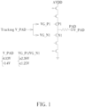
- FIG. 1 illustrates a simplified schematic diagram of one output stage circuit of IC (e.g. USB IC) of the present invention, wherein the output stage circuit is configured to communicate signals to structures external to the integrated circuit, please note that FIG. 1 is only an example and not a limitation of the present invention.
- IC e.g. USB IC
- the pad e.g., signal pad of the IC, which is used to connect to the external structure of the IC, specifically, such as I/O pad
- a voltage variation range on the pad is -0.4V ⁇ 4.03V
- a maximum withstand voltage for the gate-to-drain junction of the MOS transistors within the IC under the specific manufacturing process is 1.65V as an example.
- the pad can be the signal pads PAD_DP and/or PAD_DM, wherein the signal pad PAD_DP is used for USB Data Positive (DP) signal, and the signal pad PAD_DM is used for USB Data Minus (DM) signal.
- gate voltages VG_P1 and VG_N1 of transistors P1 and N1 need to be greater than 2.38V, such that the requirement of the absolute value of gate-to-drain voltage
- the gate voltages VG_P1 and VG_N1 of MOS transistors P1 and N1 need to be lower than 1.25V, such that the requirement of the absolute value of gate-to-drain voltage
- the present invention provides a dynamic bias voltage circuit to generate a dynamic bias voltage as gate voltages of first transistors seen from or directly connected to the pad of the IC, such that the gate voltages of first transistors seen from or directly connected to the pad PAD are able to dynamically track voltage variations on the pad of the IC.
- FIG. 2 illustrates a simplified schematic diagram of a dynamic bias voltage circuit according to one embodiment.
- the dynamic bias voltage circuit of the present invention can be used to provide bias voltage for specific transistors of an output stage of an integrated circuit.
- an integrated circuit may comprise an output stage circuit and a dynamic bias voltage circuit of the present invention.
- a dynamic bias voltage circuit 100 comprises a buffer circuit 110, a voltage divider circuit 120 and a voltage follower circuit 130.
- V1 i.e., a reference voltage
- V2 F1*V1 (F1 being a conversion factor and typically lower than or equal to 1).
- V_PAD voltage V2 outputted by the buffer circuit 110 has a high driving capability and may be not affected by the following circuits/voltages
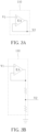
- FIG. 3A and FIG. 3B illustrates possible implementations of the buffer circuit 110 according to various embodiments of the present invention.
- the buffer circuit 110 could take the form of a unity gain buffer or a combination of a unity gain buffer and a voltage divider circuit.
- the buffer circuit 110 could be any other type of circuitry that is based on a buffer.
- the buffer or the unity gain buffer could be implemented using an amplifier (e.g., error amplifier) in a negative feedback configuration. As shown in FIG. 3A and FIG.
- the buffer circuit may comprise an error amplifier (EA) having a first input terminal (positive input terminal), a second input terminal (negative input terminal) and an output terminal, wherein the first input terminal receives the first voltage, and the second input terminal is coupled to the output terminal.
- EA error amplifier
- the output terminal of the amplifier outputs the second voltage and the second voltage may equal to the first voltage.
- the second voltage is generated based on the output voltage of the amplifier and the second voltage is less or lower than the first voltage.
- the voltage divider circuit 120 coupled to an output of the buffer circuit 110, is configured to implement a voltage division function to provide a third voltage V3 according to a pad voltage V_PAD on a pad (PAD) and the second voltage V2 outputted by the buffer circuit 110.
- the voltage divider circuit 120 may be equivalent to include resistors R3 and R4 that are connected in series.
- the pad voltage V_PAD is coupled to one end of the resistor R3, the second voltage V2 is coupled to one end of the resistor R4, and the third voltage V3 is generated at a node 125 between resistors R3 and R4.
- the voltage divider circuit 120 may include other types of resistor networks, which have more resistors or components in addition to resistors R3 and R4.
- the third voltage V3 can track voltage variations of the pad voltage V_PAD.
- a driving capability at the node 125 (which outputs the third voltage V3) of the voltage divider circuit 120 is pretty weak.
- the dynamic bias voltage circuit 100 may further include the voltage follower circuit 130 to enhance the driving capability.
- FIG. 4 illustrates a detailed schematic diagram of the dynamic bias voltage circuit according to one embodiment of the present invention.
- the dynamic bias voltage circuit 100 may further include a voltage generating circuit 105, and the buffer circuit 110 is further coupled to a voltage generating circuit 105.
- the voltage generating circuit 105 is configured to provide or generate the first voltage V1.
- the voltage generating circuit 105 may be equivalent to include resistors R1 and R2 that are connected in series, and the first voltage V1 is generated by dividing a power supply voltage AVDD (e.g. 3.3V) through resistors R1 and R2.
- AVDD e.g. 3.3V
- the voltage generating circuit 105 may include other types of resistor networks, which have more resistors or components in addition to resistors R1 and R2, to meet different design requirements.
- the voltage generating circuit 105 can be implemented by a bandgap reference circuit (i.e., bandgap reference voltage generator).
- the voltage follower circuit 130 is configured to generate a bias voltage VP according to the third voltage V3 provided by the voltage divider circuit 120.
- the voltage follower circuit 130 is characterized by very high input impedance and can be used to isolate input and output signals, thus the bias voltage VP may be not affected by the following circuits/voltages.
- the generated bias voltage VP can be applied to gates of the first transistors seen from or directly connected to an IC pad. Taking circuitry of FIG. 1 as an example, if the pad PAD of FIG. 4 is the pad PAD of FIG. 1 , the generated bias voltage VP can be applied to gates of transistors P1 and N1.
- the voltage follower circuit 130 may include a source follower, which can be implemented by the transistor M3 as shown in FIG. 4 .
- the voltage follower circuit 130 may further comprise transistors M2 and M4.
- the third voltage V3 is coupled to a control end (e.g., gate) of the transistor M3, and the bias voltage VP is output from an output terminal of the dynamic bias voltage circuit 100 that is between the transistors M3 and M4.
- control ends of the transistors M2 and M4 are coupled to fixed bias voltages V4 and V5, respectively.
- the number of transistors included in the voltage follower circuit 130 is not a limitation of the present invention.
- the number of MOS transistors included in the voltage follower circuit 130 is associated with a level of the power supply voltage AVDD.
- the power supply voltage AVDD is 3.3V
- the maximum withstand voltage for the gate-to-drain junctions of the MOS transistors is 1.65V
- the arrangement and the number of the MOS transistors in the voltage follower circuit 130 could be identical to that shown in FIG. 4 .
- the transistors M2, M3 and M4 are P-channel Metal Oxide Semiconductor (PMOS) transistors.
- the dynamic bias voltage circuit may further include a current mirror circuit 107, which is configured to generate an operating current I1 for the voltage follower circuit 130.
- the current mirror circuit 107 may comprise at least one current mirror which may include transistors M0 and M6 shown in FIG. 4 .
- the current mirror circuit 107 mirrors a reference current I0 to generate the operating current I1.
- the current mirror circuit 107 may have more current mirrors, for example, enabling the generation of the reference current I0 by mirroring another reference current, thus, a large current can be obtained from a small current. It should be noted that the generation an operating current I1 is not limited to a current mirror circuit.
- the voltage generating circuit 105 generates the first voltage V1 (i.e., reference voltage) by dividing the power supply voltage AVDD using the resistors R1 and R2.
- V 1 R 2 R 1 + R 2 ⁇ AVDD
- the voltage VSG M3 is a source-to-gate voltage of the transistor M3, which is equal to VS M3 -VG M3 , wherein VS M3 is a source voltage of the transistor M3 and VG M3 is a gate voltage of the transistor M3.
- a relationship between the source-to-gate voltage VSG M3 of the transistor M3 and the operating current I1 is as follows: VSG M 3 ⁇ I 1 K
- K is a constant, for example, which is associated with the size of the transistor M3 in the voltage follower circuit 130 under the given manufacturing process.
- the source-to-gate voltage VSG M3 would be known.
- the source-to-gate voltage VSG M3 actually can be determined based on the magnitude of the operating current I1 and the size of the transistor M3 under the specific or given manufacturing process.
- the source-to-gate voltage VSG M3 is usually in the range of several hundred millivolts (e.g., 400-500 mV).
- the bias voltage VP equals a summation of the third voltage V3 (which is associated with the pad voltage V_PAD) and a fixed voltage (which is VSG M3 ).
- the dynamic bias voltage circuit 100 is capable of dynamically tracking the pad voltage V_PAD.
- the values a and b can be determined.
- the preset values Va and Vb can be obtained or determined according to the requirement of
- the preset values Va and Vb are associated with (or limited by) the voltage variation range and the maximum withstand voltage V_W.
- the resistance relationship between the resistors R3 and R4 can be obtained or determined according to the upper bound b and the lower bound a of the voltage variation range of the pad voltage V_PAD, as well as the maximum withstand voltage V_W, wherein the preset values of the bias voltages VP (i.e., Va and Vb) are associated with the voltage variation range and the maximum withstand voltage V_W.
- the bias voltages VP i.e., Va and Vb
- the resistance relationship between the resistors R1 and R2 could also be obtained or determined at least according to the voltage variation range of the pad voltage V_PAD and the maximum withstand voltage V_W, for example, according to values a, b, Va and Vb (which are associated with the voltage variation range and the maximum withstand voltage V_W), as well as the power supply voltage AVDD and the source-to-gate voltage VSG M3 of the transistor M3.
- the bias voltage VP provided by the dynamic bias voltage circuit 100 will be applied to the gate of the first transistor seen from (or directly connected to) the pad PAD (e.g., I/O pad).
- the pad voltage V_PAD is at lower bound a
- of the first MOS transistor seen from the pad PAD would be "Va-a", which needs to be smaller than the maximum withstand voltage V_W for the gate-to-drain junction.
- the preset value Va of the bias voltage VP can be any suitable value lower than "a+V_W".
- of the first MOS transistor seen from the pad PAD would be "b-Vb", which needs to be smaller than the maximum withstand voltage V_W for the gate-to-drain junction.
- the value Vb of the bias voltage VP can be any suitable value greater than "b-V_W”.
- the pad voltage V_PAD varies from -0.4V to 4.03V
- the maximum withstand voltage V_W for the gate-to-drain junction is 1.65V
- the value Va of the bias voltage VP could be any suitable value smaller than 1.25V
- the value Vb of the bias voltage VP could be any suitable value greater than 2.38.
- value Vb of the bias voltage VP needs to be smaller than the power supply voltage AVDD (e.g., 3.3V).
- the driving capability of the dynamic bias voltage circuit 100 can be adjusted by varying the magnitude of operating current I1.
- the magnitude of the reference current I0 is equivalent to proportionally adjusting the magnitude of the operating current I1. Therefore, enlarging the magnitude of the reference current I0 is equivalent to enhancing the driving capability of the voltage follower circuit 130, because the greater the operating current I1, the stronger the driving ability of the voltage follower circuit 130.
- the integrated circuit may comprise a normal operating mode and a power-saving mode.
- the operating current I1 has a first current value
- the power-saving mode the operating current I1 has a second current value which is less than the first current value.
- the normal operating mode refers to a full-speed transmission (FSTX) mode
- the operating current I1 for the voltage follower circuit 130 needs to be higher to enhance the driving ability, thereby to avoid being interfered by the signal on the pad PAD (which may affect the performance of the dynamic bias voltage circuit 100) and have high driving capability.
- the operating current I1 could be lower for reducing power consumption. Therefore, in some embodiments, different values of the operating current I1 can be set in advance for different operating modes. For example, the first current value can be set for the FSTX mode, and the second current value can be set for the power-saving mode, where the first current value is larger than the second current value.
- the dynamic bias voltage circuit 100 of the present invention can be used with ICs other than USB ICs, thereby ensuring that the gate-to-drain voltage
Landscapes
- Engineering & Computer Science (AREA)
- Physics & Mathematics (AREA)
- Electromagnetism (AREA)
- General Physics & Mathematics (AREA)
- Radar, Positioning & Navigation (AREA)
- Automation & Control Theory (AREA)
- Microelectronics & Electronic Packaging (AREA)
- Nonlinear Science (AREA)
- Computer Hardware Design (AREA)
- Computing Systems (AREA)
- General Engineering & Computer Science (AREA)
- Mathematical Physics (AREA)
- Amplifiers (AREA)
- Semiconductor Integrated Circuits (AREA)
Abstract
A dynamic bias voltage circuit (100) for providing a bias voltage (VP) includes: a buffer circuit (110), a voltage divider circuit (120) and a voltage follower circuit (130). The buffer circuit (110) is configured to output a second voltage (V2) according to a first voltage (V1). The voltage divider circuit (120) is coupled to the buffer circuit (110) and configured to implement a voltage division function to provide a third voltage (V3) according to the second voltage (V2) and a pad voltage (V_PAD) on a pad (PAD) of the integrated circuit (100). The voltage follower circuit (130) is coupled to the voltage divider circuit (120) and configured to generate the bias voltage (VP) according to the third voltage (V3).
Description
- The present invention relates to integrated circuits, and more particular to a dynamic bias voltage circuit for providing a dynamic bias voltage to specific transistors of an integrated circuit.
- In applications for Universal Serial Bus (USB) 2.0, a voltage variation range on signal pads of USB integrated circuits (ICs) can be significantly varied from -0.4V to 4.03V Considering certain semiconductor manufacturing processes, a maximum withstand voltage for gate-to-drain junctions of Metal-Oxide-Semiconductor (MOS) transistors may be small, and for example could be even limited to 1.65V (e.g. in a 3nm process). Therefore, if a bias voltage at the gate of a MOS transistor is statically set, it might prove challenging to meet reliability requirements given the wide voltage variation range on the pads.
- In view of this, it is one object of the present invention to provide a dynamic bias voltage circuit that is operable to dynamically track voltage variations on IC pads. The dynamic bias voltage circuit of the present invention generates a bias voltage for first transistors seen from or directly connected with the IC pads. This ensures that the absolute value of gate-to-drain voltages of the first transistors seen from or directly connected with the pads would not exceed a maximum withstand voltage imposed by their manufacturing process, although the voltage variation range on the pads is wide. A dynamic bias voltage circuit and an integrated circuit according to the invention are defined in the independent claims. The dependent claims define preferred embodiments thereof.
- According to some embodiments of the present invention, a dynamic bias voltage circuit for providing a bias voltage to at least one specific transistor of an integrated circuit is provided. The dynamic bias voltage circuit comprises: a buffer circuit, a voltage divider circuit and a voltage follower circuit. The buffer circuit is configured to output a second voltage according to a first voltage. The voltage divider circuit is coupled to the buffer circuit and configured to provide a third voltage according to the second voltage and a pad voltage on a pad of the integrated circuit. The voltage follower circuit is coupled to the voltage divider circuit and configured to generate the bias voltage according to the third voltage.
- Preferably, the buffer circuit comprises an amplifier, which has a first input terminal, a second input terminal and an output terminal, wherein the first input terminal receives the first voltage, and the second input terminal is coupled to the output terminal. Additionally, the output terminal of the amplifier outputs the second voltage, and the second voltage equals the first voltage. Alternatively, the second voltage is generated based on the output voltage of the amplifier and the second voltage is less than the first voltage.
- Preferably, the dynamic bias voltage circuit further comprises a voltage generating circuit, coupled to the buffer circuit, configured to generate the first voltage by dividing a power supply voltage through a resistor network. Additionally, the resistor network comprises a first resistor and a second resistor connected in series.
- Preferably, the voltage divider circuit comprises a third resistor and a fourth resistor connected in series, wherein the third voltage is generated at a node between the third resistor and the fourth resistor.
- Preferably, a first end of the third resistor is coupled to the pad voltage, a second end of the third resistor is coupled to a first end of the fourth resistor, and a second end of the fourth resistor is coupled to the second voltage.
- Preferably, the resistance relationship between the third resistor and the fourth resistor is associated with a voltage variation range of the pad voltage and a maximum withstand voltage imposed by specific manufacturing process of the integrated circuit.
- Preferably, the voltage follower circuit comprises a first transistor, a second transistor and a third transistor. The first transistor has a control end, a first end and a second end, wherein the control end of the first transistor is coupled to a first fixed voltage, the first end of the first transistor is coupled to a power supply voltage. The second transistor has a control end, a first end and a second end, wherein the control end of the second transistor is coupled to the third voltage, the first end of the second transistor is coupled to the second end of the first transistor, the node between the first transistor and the second transistor serves as an output terminal of the voltage follower circuit. The third transistor has a control end, a first end and a second end, wherein the control end of the third transistor is coupled to a second fixed voltage, the first end of the third transistor is coupled to the second end of the second transistor, and the second end of the third transistor is coupled to the ground.
- Preferably, the voltage follower circuit comprises a source follower, which is implemented by a transistor.
- Preferably, the dynamic bias voltage circuit further comprises a current mirror circuit, configured to provide an operating current for the voltage follower circuit.
- Preferably, the bias voltage is associated with the pad voltage and the operating current.
- Preferably, the integrated circuit comprises a normal operating mode and a power-saving mode; during the normal operating mode, the operating current has a first current value, and during the power-saving mode, the operating current has a second current value which is less than the first current value.
- Preferably, the integrated circuit is compliant with Universal Serial Bus (USB) standard, and the integrated circuit comprises a full-speed transmission (FSTX) mode and a power-saving mode, during the FSTX mode, the operating current has a first current value, and during the power-saving mode, the operating current has a second current value which is less than the first current value.
- Preferably, the at least one specific transistor to which the bias voltage is provided is at least one of first transistors seen from or directly connected to the pad of the integrated circuit and the bias voltage is coupled to a control end of the at least one specific transistor.
- According to some embodiments of the present invention, an integrated circuit is provided. The integrated circuit comprises: an output stage circuit and a dynamic bias voltage circuit. The output stage circuit is configured to communicate signals to structures external to the integrated circuit. The dynamic bias voltage circuit is configured to provide a dynamic bias voltage to at least one specific transistor of the output stage circuit. The dynamic bias voltage circuit comprises: a buffer circuit, a voltage divider circuit and a voltage follower circuit. The buffer circuit is configured to output a second voltage according to a first voltage. The voltage divider circuit is coupled to the buffer circuit, and configured to implement a voltage division function to provide a third voltage according to the second voltage and a pad voltage on the pad of the integrated circuit. The voltage follower circuit is coupled to the voltage divider circuit, and configured to generate the bias voltage according to the third voltage.
- Preferably, the dynamic bias voltage circuit further comprises a voltage generating circuit, coupled to the buffer circuit, configured to generate the first voltage by dividing a power supply voltage through a resistor network. Additionally, the resistor network comprises a first resistor and a second resistor connected in series.
- Preferably, wherein the voltage divider circuit comprises a third resistor and a fourth resistor connected in series, wherein the third voltage is generated at a node between the third resistor and the fourth resistor.
- Preferably, the resistance relationship between the third resistor and the fourth resistor is associated with a voltage variation range of the pad voltage and a maximum withstand voltage imposed by specific manufacturing process of the integrated circuit.
- Preferably, the voltage follower circuit comprises a first transistor, a second transistor and a third transistor. The first transistor has a control end, a first end and a second end, wherein the control end of the first transistor is coupled to a first fixed voltage, the first end of the first transistor is coupled to a power supply voltage. The second transistor has a control end, a first end and a second end, wherein the control end of the second transistor is coupled to the third voltage, the first end of the second transistor is coupled to the second end of the first transistor, the node between the first transistor and the second transistor serves as an output terminal of the voltage follower circuit. The third transistor has a control end, a first end and a second end, wherein the control end of the third transistor is coupled to a second fixed voltage, the first end of the third is coupled to the second end of the second transistor, and the second end of the third transistor is coupled to the ground.
- Preferably, the dynamic bias voltage circuit further comprises a current mirror circuit, configured to provide an operating current for the voltage follower circuit. Additionally, the integrated circuit comprises a normal operating mode and a power-saving mode; during the normal operating mode, the operating current has a first current value, and during the power-saving mode, the operating current has a second current value which is less than the first current value.
- Preferably, the integrated circuit is compliant with Universal Serial Bus (USB) standard, the at least one specific transistor of the output stage circuit is at least one of first transistors seen from or directly connected to the pad of the integrated circuit, and the bias voltage is coupled to a control end of the at least one specific transistor.
- These and other objectives of the present invention will no doubt become obvious to those of ordinary skill in the art after reading the following detailed description of the preferred embodiment that is illustrated in the various figures and drawings.
-
-
FIG. 1 illustrates a simplified schematic diagram of an output stage circuit of USB IC. -
FIG. 2 illustrates a simplified schematic diagram of a dynamic bias voltage circuit according to one embodiment of the present invention. -
FIG. 3A and FIG. 3B illustrate possible implementations of the buffer circuit ofFIG. 2 according to various embodiments of the present invention. -
FIG. 4 illustrates a detailed schematic diagram of a dynamic bias voltage circuit according to one embodiment of the present invention. - In the following description, numerous specific details are set forth in order to provide a thorough understanding of the present embodiments. It will be apparent, however, to one having ordinary skill in the art that the specific detail need not be employed to practice the present embodiments. In other instances, well-known materials or methods have not been described in detail in order to avoid obscuring the present embodiments.
- Reference throughout this specification to "one embodiment" or "an embodiment" means that a particular feature, structure or characteristic described in connection with the embodiment or example is included in at least one embodiment of the present embodiments. Thus, appearances of the phrases "in one embodiment" or "in an embodiment" in various places throughout this specification are not necessarily all referring to the same embodiment. Furthermore, the particular features, structures or characteristics may be combined in any suitable combinations and/or sub-combinations in one or more embodiments.
- The following description is made for the purpose of illustrating the general principles of the invention and should not be taken in a limiting sense. The scope of the invention is best determined by reference to the appended claims.
FIG. 1 illustrates a simplified schematic diagram of one output stage circuit of IC (e.g. USB IC) of the present invention, wherein the output stage circuit is configured to communicate signals to structures external to the integrated circuit, please note thatFIG. 1 is only an example and not a limitation of the present invention. Specifically, taking a voltage variation range on the pad (e.g., signal pad of the IC, which is used to connect to the external structure of the IC, specifically, such as I/O pad) is -0.4V~4.03V, and a maximum withstand voltage for the gate-to-drain junction of the MOS transistors within the IC under the specific manufacturing process (e.g. 3nm process) is 1.65V as an example. In the case of the application of USB, but the invention is not limited to this, the pad can be the signal pads PAD_DP and/or PAD_DM, wherein the signal pad PAD_DP is used for USB Data Positive (DP) signal, and the signal pad PAD_DM is used for USB Data Minus (DM) signal. As shown in the diagram, when a voltage on a pad PAD of an IC (not shown) is at 4.03V (i.e., an upper bound of the voltage variation range on the pad), gate voltages VG_P1 and VG_N1 of transistors P1 and N1 (both of which are first transistors seen from (or directly connected to) the pad PAD) need to be greater than 2.38V, such that the requirement of the absolute value of gate-to-drain voltage |VGD| of the MOS transistors directly connected to the pad PAD being lower than 1.65V (i.e., the maximum withstand voltage for the gate-to-drain junction under the specific/given/certain manufacturing process) can be satisfied. On the other hand, when a voltage on a pad PAD of the IC is at -0.4V (i.e., a lower bound of the voltage variation range on the pad), the gate voltages VG_P1 and VG_N1 of MOS transistors P1 and N1 need to be lower than 1.25V, such that the requirement of the absolute value of gate-to-drain voltage |VGD| of the MOS transistors directly connected to the pad PAD being lower than 1.65V can be satisfied. In view of this, the present invention provides a dynamic bias voltage circuit to generate a dynamic bias voltage as gate voltages of first transistors seen from or directly connected to the pad of the IC, such that the gate voltages of first transistors seen from or directly connected to the pad PAD are able to dynamically track voltage variations on the pad of the IC. -
FIG. 2 illustrates a simplified schematic diagram of a dynamic bias voltage circuit according to one embodiment. Preferably, the dynamic bias voltage circuit of the present invention can be used to provide bias voltage for specific transistors of an output stage of an integrated circuit. Preferably, an integrated circuit may comprise an output stage circuit and a dynamic bias voltage circuit of the present invention. As depicted inFIG. 2 , a dynamicbias voltage circuit 100 comprises abuffer circuit 110, avoltage divider circuit 120 and avoltage follower circuit 130. Thebuffer circuit 110 has the characteristics of high input impedance and low output impedance, and thebuffer circuit 110 is configured to provide a second voltage V2 according to a first voltage V1 (i.e., a reference voltage), where V2=F1*V1 (F1 being a conversion factor and typically lower than or equal to 1). By usingbuffer circuit 110, the voltage V2 outputted by thebuffer circuit 110 has a high driving capability and may be not affected by the following circuits/voltages (e.g., V_PAD). -
FIG. 3A and FIG. 3B illustrates possible implementations of thebuffer circuit 110 according to various embodiments of the present invention. In the shown implementations, thebuffer circuit 110 could take the form of a unity gain buffer or a combination of a unity gain buffer and a voltage divider circuit. However, the scope of the present invention is not limited to these designs. In various embodiments of the present invention, thebuffer circuit 110 could be any other type of circuitry that is based on a buffer. Preferably, the buffer or the unity gain buffer could be implemented using an amplifier (e.g., error amplifier) in a negative feedback configuration. As shown inFIG. 3A and FIG. 3B , the buffer circuit may comprise an error amplifier (EA) having a first input terminal (positive input terminal), a second input terminal (negative input terminal) and an output terminal, wherein the first input terminal receives the first voltage, and the second input terminal is coupled to the output terminal. Specifically, in one embodiment as shown inFIG. 3A , the output terminal of the amplifier outputs the second voltage and the second voltage may equal to the first voltage. In another embodiment as shown inFIG. 3B , the second voltage is generated based on the output voltage of the amplifier and the second voltage is less or lower than the first voltage. - Referring back to
FIG. 2 , thevoltage divider circuit 120, coupled to an output of thebuffer circuit 110, is configured to implement a voltage division function to provide a third voltage V3 according to a pad voltage V_PAD on a pad (PAD) and the second voltage V2 outputted by thebuffer circuit 110. In this embodiment, thevoltage divider circuit 120 may be equivalent to include resistors R3 and R4 that are connected in series. The pad voltage V_PAD is coupled to one end of the resistor R3, the second voltage V2 is coupled to one end of the resistor R4, and the third voltage V3 is generated at anode 125 between resistors R3 and R4. However, in various embodiments of the present invention, thevoltage divider circuit 120 may include other types of resistor networks, which have more resistors or components in addition to resistors R3 and R4. - As shown in
FIG. 2 , the third voltage V3 can be expressed as follows:
- In view of above, it can be understood that the third voltage V3 can track voltage variations of the pad voltage V_PAD. Please note that a driving capability at the node 125 (which outputs the third voltage V3) of the
voltage divider circuit 120 is pretty weak. Hence, the dynamicbias voltage circuit 100 may further include thevoltage follower circuit 130 to enhance the driving capability. -
FIG. 4 illustrates a detailed schematic diagram of the dynamic bias voltage circuit according to one embodiment of the present invention. As depicted inFIG. 4 , the dynamicbias voltage circuit 100 may further include avoltage generating circuit 105, and thebuffer circuit 110 is further coupled to avoltage generating circuit 105. Thevoltage generating circuit 105 is configured to provide or generate the first voltage V1. For example, thevoltage generating circuit 105 may be equivalent to include resistors R1 and R2 that are connected in series, and the first voltage V1 is generated by dividing a power supply voltage AVDD (e.g. 3.3V) through resistors R1 and R2. Please note that, according to various embodiments of the present invention, thevoltage generating circuit 105 may include other types of resistor networks, which have more resistors or components in addition to resistors R1 and R2, to meet different design requirements. Moreover, in various embodiments of the present invention, thevoltage generating circuit 105 can be implemented by a bandgap reference circuit (i.e., bandgap reference voltage generator). - On the other hand, the
voltage follower circuit 130 is configured to generate a bias voltage VP according to the third voltage V3 provided by thevoltage divider circuit 120. Please note that thevoltage follower circuit 130 is characterized by very high input impedance and can be used to isolate input and output signals, thus the bias voltage VP may be not affected by the following circuits/voltages. The generated bias voltage VP can be applied to gates of the first transistors seen from or directly connected to an IC pad. Taking circuitry ofFIG. 1 as an example, if the pad PAD ofFIG. 4 is the pad PAD ofFIG. 1 , the generated bias voltage VP can be applied to gates of transistors P1 and N1. - In this embodiment, the
voltage follower circuit 130 may include a source follower, which can be implemented by the transistor M3 as shown inFIG. 4 . In addition, thevoltage follower circuit 130 may further comprise transistors M2 and M4. The third voltage V3 is coupled to a control end (e.g., gate) of the transistor M3, and the bias voltage VP is output from an output terminal of the dynamicbias voltage circuit 100 that is between the transistors M3 and M4. Additionally, control ends of the transistors M2 and M4 are coupled to fixed bias voltages V4 and V5, respectively. Please note that, the number of transistors included in thevoltage follower circuit 130 is not a limitation of the present invention. Actually, the number of MOS transistors included in thevoltage follower circuit 130 is associated with a level of the power supply voltage AVDD. In the case where the power supply voltage AVDD is 3.3V, and the maximum withstand voltage for the gate-to-drain junctions of the MOS transistors is 1.65V, the arrangement and the number of the MOS transistors in thevoltage follower circuit 130 could be identical to that shown inFIG. 4 . However, in various embodiments of the present invention, there could be more or fewer MOS transistors included in thevoltage follower circuit 130. Preferably, the transistors M2, M3 and M4 are P-channel Metal Oxide Semiconductor (PMOS) transistors. - As shown in
FIG. 4 , the dynamic bias voltage circuit may further include acurrent mirror circuit 107, which is configured to generate an operating current I1 for thevoltage follower circuit 130. For example, thecurrent mirror circuit 107 may comprise at least one current mirror which may include transistors M0 and M6 shown inFIG. 4 . Specifically, thecurrent mirror circuit 107 mirrors a reference current I0 to generate the operating current I1. Moreover, in various embodiments of the present invention, thecurrent mirror circuit 107 may have more current mirrors, for example, enabling the generation of the reference current I0 by mirroring another reference current, thus, a large current can be obtained from a small current. It should be noted that the generation an operating current I1 is not limited to a current mirror circuit. - In the embodiment shown by
FIG. 4 , thevoltage generating circuit 105 generates the first voltage V1 (i.e., reference voltage) by dividing the power supply voltage AVDD using the resistors R1 and R2. Thus, in the case of thebuffer circuit 110 is a unity gain buffer, the first voltage V1 and the second voltage V2 can be expressed as follows:
- Hence, in the embodiments as depicted in
FIG. 2 andFIG. 4 , the third voltage V3 provided by thevoltage divider circuit 120 can be expressed as follows:
- Further, the bias voltage VP generated by the
voltage follower circuit 130 can be expressed as:
- Here, the voltage VSGM3 is a source-to-gate voltage of the transistor M3, which is equal to VSM3-VGM3, wherein VSM3 is a source voltage of the transistor M3 and VGM3 is a gate voltage of the transistor M3. In addition, a relationship between the source-to-gate voltage VSGM3 of the transistor M3 and the operating current I1 is as follows:

- Here, K is a constant, for example, which is associated with the size of the transistor M3 in the
voltage follower circuit 130 under the given manufacturing process. Hence, for a specific magnitude of the operating current I1, the source-to-gate voltage VSGM3 would be known. For example, the source-to-gate voltage VSGM3 actually can be determined based on the magnitude of the operating current I1 and the size of the transistor M3 under the specific or given manufacturing process. For illustrative purposes, the source-to-gate voltage VSGM3 is usually in the range of several hundred millivolts (e.g., 400-500 mV). - As can be comprehended from the expression of the bias voltage VP, the bias voltage VP equals a summation of the third voltage V3 (which is associated with the pad voltage V_PAD) and a fixed voltage (which is VSGM3). In view of this, the dynamic
bias voltage circuit 100 is capable of dynamically tracking the pad voltage V_PAD. - Moreover, assume that the voltage variation range of the pad voltage V_PAD varies from a to b, a first preset value of the bias voltage VP is represented as "Va" at the condition of V_PAD=a (the lower bound of the voltage variation range) and a second preset value of the bias voltage VP is represented as "Vb" at the condition of V_PAD=b (the upper bound of the voltage variation range), the above-mentioned expression of the bias voltage VP can be rewritten as follows:


- Further, the above equations can be converted into:


- In view of above, through the voltage variation range of the pad voltage V_PAD, the values a and b can be determined. Moreover, through the maximum withstand voltage V_W for gate-to-drain junction imposed by the manufacturing process, the preset values Va and Vb can be obtained or determined according to the requirement of |VGD|< V_W, that is to say, "Va-a<V_W" as well as "b-Vb<V_W", hence, "Va<a+V_W" and "Vb>b-V_W". Please note that, the preset values Va and Vb are associated with (or limited by) the voltage variation range and the maximum withstand voltage V_W. Further, a resistance relationship between resistors R3 and R4 can be further expressed as follows:
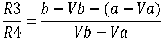
- In view of above, the resistance relationship between the resistors R3 and R4 can be obtained or determined according to the upper bound b and the lower bound a of the voltage variation range of the pad voltage V_PAD, as well as the maximum withstand voltage V_W, wherein the preset values of the bias voltages VP (i.e., Va and Vb) are associated with the voltage variation range and the maximum withstand voltage V_W. Moreover, the resistance relationship between the resistors R1 and R2 could also be obtained or determined at least according to the voltage variation range of the pad voltage V_PAD and the maximum withstand voltage V_W, for example, according to values a, b, Va and Vb (which are associated with the voltage variation range and the maximum withstand voltage V_W), as well as the power supply voltage AVDD and the source-to-gate voltage VSGM3 of the transistor M3.
- As mentioned above, the bias voltage VP provided by the dynamic
bias voltage circuit 100 will be applied to the gate of the first transistor seen from (or directly connected to) the pad PAD (e.g., I/O pad). Hence, when the pad voltage V_PAD is at lower bound a, the gate-to-drain voltage |VGD| of the first MOS transistor seen from the pad PAD would be "Va-a", which needs to be smaller than the maximum withstand voltage V_W for the gate-to-drain junction. In other words, the preset value Va of the bias voltage VP can be any suitable value lower than "a+V_W". On the other hand, when the pad voltage V_PAD is at the upper bound b, the gate-to-drain voltage |VGD| of the first MOS transistor seen from the pad PAD would be "b-Vb", which needs to be smaller than the maximum withstand voltage V_W for the gate-to-drain junction. In other words, the value Vb of the bias voltage VP can be any suitable value greater than "b-V_W". Assume that the pad voltage V_PAD varies from -0.4V to 4.03V, and the maximum withstand voltage V_W for the gate-to-drain junction is 1.65V, the value Va of the bias voltage VP could be any suitable value smaller than 1.25V, and the value Vb of the bias voltage VP could be any suitable value greater than 2.38. Also, value Vb of the bias voltage VP needs to be smaller than the power supply voltage AVDD (e.g., 3.3V). - Preferably, the driving capability of the dynamic
bias voltage circuit 100 can be adjusted by varying the magnitude of operating current I1. For example, suppose a size ratio of the transistor M0 to the transistor M6 is 1:n, then the ratio of the magnitude of the reference current I0 to that of the operating current I1 will be 1:n. Thus, adjusting the magnitude of the reference current I0 is equivalent to proportionally adjusting the magnitude of the operating current I1. Therefore, enlarging the magnitude of the reference current I0 is equivalent to enhancing the driving capability of thevoltage follower circuit 130, because the greater the operating current I1, the stronger the driving ability of thevoltage follower circuit 130. Also, since the magnitude of the operating current I1 and the source-to-gate voltage of the transistor M3 VSGM3 have an exponential relationship, the influence of the magnitude of the operating current I1 on the outputted bias voltage VP is relatively small. Thus, a certain voltage margin can be reserved when the preset Va and Vb are set. - Preferably, the integrated circuit may comprise a normal operating mode and a power-saving mode. During the normal operating mode, the operating current I1 has a first current value, and during the power-saving mode, the operating current I1 has a second current value which is less than the first current value. Specifically, in the application for USB 2.0, the normal operating mode refers to a full-speed transmission (FSTX) mode, when the USB IC is operated in the FSTX mode, the operating current I1 for the
voltage follower circuit 130 needs to be higher to enhance the driving ability, thereby to avoid being interfered by the signal on the pad PAD (which may affect the performance of the dynamic bias voltage circuit 100) and have high driving capability. However, when the USB IC is operated in a power-saving mode, almost circuits in USB IC may stop operating, but the dynamicbias voltage circuit 100 still needs to operate. Hence, the operating current I1 could be lower for reducing power consumption. Therefore, in some embodiments, different values of the operating current I1 can be set in advance for different operating modes. For example, the first current value can be set for the FSTX mode, and the second current value can be set for the power-saving mode, where the first current value is larger than the second current value. - Please note that while the USB 2.0 related voltage variation range (e.g., -0.4V to 4.03V) and the maximum withstand voltage (e.g., 1.65V) of specific manufacturing process have been extensively mentioned to explain the concept of the present invention, it is not intended to limit the present invention in scope. The dynamic
bias voltage circuit 100 of the present invention can be used with ICs other than USB ICs, thereby ensuring that the gate-to-drain voltage |VGD| of the first transistor seen from IC pads (e.g., I/O pad) will not exceed the maximum withstand voltage imposed by specific manufacturing process of the IC. Therefore, the present invention effectively ensures the reliability requirement of MOS transistors under specific manufacturing process. - Those skilled in the art will readily observe that numerous modifications and alterations of the device and method may be made while retaining the teachings of the invention. Accordingly, the above disclosure should be construed as limited only by the metes and bounds of the appended claims.
Claims (15)
- A dynamic bias voltage circuit (100) for providing a dynamic bias voltage (VP) to at least one specific transistor (P1, N1) of an integrated circuit, comprising:a buffer circuit (110), configured to output a second voltage (V2) according to a first voltage (V1);a voltage divider circuit (120), coupled to the buffer circuit (110), configured to implement a voltage division function to provide a third voltage (V3) according to the second voltage (V2) and a pad voltage (V_PAD) on a pad (PAD) of the integrated circuit; anda voltage follower circuit (130), coupled to the voltage divider circuit (120), configured to generate the bias voltage (VP) according to the third voltage (V3).
- The dynamic bias voltage circuit (100) of claim 1, wherein the buffer circuit (110) comprisesan amplifier (EA) having a first input terminal, a second input terminal and an output terminal, wherein the first input terminal receives the first voltage (V1), and the second input terminal is coupled to the output terminal;wherein the output terminal of the amplifier outputs the second voltage (V2), and the second voltage (V2) equals the first voltage (V1); orwherein the second voltage (V2) is generated based on the output voltage of the amplifier (EA) and the second voltage (V2) is less than the first voltage (V1).
- The dynamic bias voltage circuit (100) of claim 1 or 2, further comprising:a voltage generating circuit (105), coupled to the buffer circuit (110), configured to generate the first voltage (V1) by dividing a power supply voltage (AVDD) through a resistor network;wherein the resistor network comprises a first resistor (R1) and a second resistor (R2) connected in series.
- The dynamic bias voltage circuit (100) of any one of claims 1 to 3, wherein the voltage divider circuit (120) comprises:
a third resistor (R3) and a fourth resistor (R4) connected in series, wherein the third voltage (V3) is generated at a node between the third resistor (R3) and the fourth resistor (R4). - The dynamic bias voltage circuit (100) of claim 4, wherein a first end of the third resistor (R3) is coupled to the pad voltage (V_PAD), a second end of the third resistor (R3) is coupled to a first end of the fourth resistor (R4), and a second end of the fourth resistor (R4) is coupled to the second voltage (V2).
- The dynamic bias voltage circuit (100) of claim 4 or 5, wherein the resistance relationship between the third resistor (R3) and the fourth resistor (R4) is associated with a voltage variation range of the pad voltage (V_PAD) and a maximum withstand voltage imposed by specific manufacturing process of the integrated circuit.
- The dynamic bias voltage circuit (100) of any one of claims 1 to 6, wherein the voltage follower circuit (130) comprises:a first transistor (M4), having a control end, a first end and a second end, wherein the control end of the first transistor (M4) is coupled to a first fixed voltage (V5), the first end of the first transistor is coupled to a power supply voltage;a second transistor (M3), having a control end, a first end and a second end, wherein the control end of the second transistor (M3) is coupled to the third voltage (V3), the first end of the second transistor (M3) is coupled to the second end of the first transistor (M4), the node between the first transistor (M4) and the second transistor (M3) serves as an output terminal of the voltage follower circuit (130); anda third transistor (M2), having a control end, a first end and a second end, wherein the control end of the third transistor (M2) is coupled to a second fixed voltage (V4), the first end of the third transistor (M2) is coupled to the second end of the second transistor (M3), and the second end of the third transistor (M2) is coupled to the ground.
- The dynamic bias voltage circuit (100) of any one of claims 1 to 7, wherein the voltage follower circuit (130) comprises a source follower, which is implemented by a transistor (M3).
- The dynamic bias voltage circuit (100) of claim 8, further comprising:
a current mirror circuit (107), configured to provide an operating current (I1) for the voltage follower circuit (130). - The dynamic bias voltage circuit (100) of any one of claims 1 to 9, wherein the bias voltage (VP) is associated with the pad voltage (V_PAD) and the operating current (I1).
- The dynamic bias voltage circuit (100) of any one of claims 1 to 10, wherein the voltage follower circuit is further configured to receive an operating current (I1) and the integrated circuit comprises a normal operating mode and a power-saving mode; during the normal operating mode, the operating current (I1) has a first current value, and during the power-saving mode, the operating current (I1) has a second current value which is less than the first current value.
- The dynamic bias voltage circuit (100) of any one of claims 1 to 11, wherein the voltage follower circuit is further configured to receive an operating current (I1) and the integrated circuit is compliant with Universal Serial Bus, in the following also referred to as USB, standard, and the integrated circuit comprises a full-speed transmission, in the following also referred to as FSTX, mode and a power-saving mode, during the FSTX mode, the operating current (I1) has a first current value, and during the power-saving mode, the operating current (I1) has a second current value which is less than the first current value.
- The dynamic bias voltage circuit (100) of any one of claims 1 to 12, wherein the at least one specific transistor (P1, N1) to which the bias voltage (VP) is provided is at least one of first transistors (P1, N1) seen from or directly connected to the pad (PAD) of the integrated circuit and the bias voltage (VP) is coupled to a control end of the at least one specific transistor (P1, N1).
- An integrated circuit, comprising:an output stage circuit, configured to communicate signals to structures external to the integrated circuit; anda dynamic bias voltage circuit (100) according to any one of the preceding claims, wherein the at least one specific transistor (P1, N1) is comprised in the output stage circuit.
- The integrated circuit of claim 14, wherein the integrated circuit is compliant with USB standard, the at least one specific transistor (P1, N1) of the output stage circuit is at least one of first transistors (P1, N1) seen from or directly connected to the pad (PAD) of the integrated circuit, and the bias voltage (VP) is coupled to a control end of the at least one specific transistor (P1, N1).
Applications Claiming Priority (1)
| Application Number | Priority Date | Filing Date | Title |
|---|---|---|---|
| CN202311072109.1A CN119512290A (en) | 2023-08-23 | 2023-08-23 | A dynamic bias voltage circuit and integrated circuit |
Publications (1)
| Publication Number | Publication Date |
|---|---|
| EP4513760A1 true EP4513760A1 (en) | 2025-02-26 |
Family
ID=88236395
Family Applications (1)
| Application Number | Title | Priority Date | Filing Date |
|---|---|---|---|
| EP23200556.1A Pending EP4513760A1 (en) | 2023-08-23 | 2023-09-28 | Dynamic bias voltage circuit and integrated circuit |
Country Status (3)
| Country | Link |
|---|---|
| US (1) | US12517533B2 (en) |
| EP (1) | EP4513760A1 (en) |
| CN (1) | CN119512290A (en) |
Citations (2)
| Publication number | Priority date | Publication date | Assignee | Title |
|---|---|---|---|---|
| US20050088199A1 (en) * | 2003-10-28 | 2005-04-28 | Bales Tim J. | Mos linear region impedance curvature correction |
| US20210409020A1 (en) * | 2020-06-26 | 2021-12-30 | Advanced Micro Devices, Inc. | High voltage output circuit with low voltage devices using data dependent dynamic biasing |
Family Cites Families (3)
| Publication number | Priority date | Publication date | Assignee | Title |
|---|---|---|---|---|
| US9772637B2 (en) * | 2013-06-07 | 2017-09-26 | Mediatek Inc. | Voltage regulation circuits and power supply devices using the same |
| US11716073B2 (en) * | 2021-04-07 | 2023-08-01 | Mediatek Inc. | Chip with pad tracking |
| FR3148849A1 (en) * | 2023-05-15 | 2024-11-22 | Commissariat A L'energie Atomique Et Aux Energies Alternatives | Reference voltage generation circuit |
-
2023
- 2023-08-23 CN CN202311072109.1A patent/CN119512290A/en active Pending
- 2023-09-14 US US18/368,528 patent/US12517533B2/en active Active
- 2023-09-28 EP EP23200556.1A patent/EP4513760A1/en active Pending
Patent Citations (2)
| Publication number | Priority date | Publication date | Assignee | Title |
|---|---|---|---|---|
| US20050088199A1 (en) * | 2003-10-28 | 2005-04-28 | Bales Tim J. | Mos linear region impedance curvature correction |
| US20210409020A1 (en) * | 2020-06-26 | 2021-12-30 | Advanced Micro Devices, Inc. | High voltage output circuit with low voltage devices using data dependent dynamic biasing |
Also Published As
| Publication number | Publication date |
|---|---|
| US20250068198A1 (en) | 2025-02-27 |
| CN119512290A (en) | 2025-02-25 |
| US12517533B2 (en) | 2026-01-06 |
Similar Documents
| Publication | Publication Date | Title |
|---|---|---|
| US10541677B2 (en) | Low output impedance, high speed and high voltage generator for use in driving a capacitive load | |
| EP0372956B1 (en) | Constant current source circuit | |
| CN111316188B (en) | Low-dropout linear voltage stabilizing system | |
| US10454466B1 (en) | Biasing cascode transistors of an output buffer circuit for operation over a wide range of supply voltages | |
| US6380799B1 (en) | Internal voltage generation circuit having stable operating characteristics at low external supply voltages | |
| US20090021292A1 (en) | Reliable level shifter of ultra-high voltage device used in low power application | |
| US6894555B2 (en) | Bandgap reference circuit | |
| CN109213248A (en) | Negative electricity source control circuit and power supply device | |
| CN118174530B (en) | Soft start circuit utilizing operational amplifier mismatch characteristic | |
| US7564225B2 (en) | Low-power voltage reference | |
| CN111446949B (en) | Power-on reset circuit and integrated circuit | |
| US6759878B2 (en) | Voltage comparator circuit and substrate bias adjusting circuit using same | |
| US6784700B1 (en) | Input buffer circuit | |
| CN116520935A (en) | Low-dropout linear voltage regulator | |
| US6127854A (en) | Differential comparator with stable switching threshold | |
| CN101160721A (en) | Apparatus and method for adaptive trip point detection | |
| JP2010028867A (en) | Level conversion circuit | |
| US12517533B2 (en) | Dynamic bias voltage circuit and integrated circuit | |
| US8987949B1 (en) | Linear regulator with multiple outputs and local feedback | |
| CN112798919B (en) | Power supply low-voltage monitoring circuit based on FGD NMOS tube | |
| US20210218391A1 (en) | Comparator circuit | |
| KR20220104021A (en) | Buffer devices, chips and electronics | |
| CN116243750B (en) | Voltage stabilizer circuit, chip and electronic equipment | |
| US12512801B2 (en) | Squelch detector | |
| JP2985673B2 (en) | Delay circuit |
Legal Events
| Date | Code | Title | Description |
|---|---|---|---|
| PUAI | Public reference made under article 153(3) epc to a published international application that has entered the european phase |
Free format text: ORIGINAL CODE: 0009012 |
|
| STAA | Information on the status of an ep patent application or granted ep patent |
Free format text: STATUS: REQUEST FOR EXAMINATION WAS MADE |
|
| 17P | Request for examination filed |
Effective date: 20240816 |
|
| AK | Designated contracting states |
Kind code of ref document: A1 Designated state(s): AL AT BE BG CH CY CZ DE DK EE ES FI FR GB GR HR HU IE IS IT LI LT LU LV MC ME MK MT NL NO PL PT RO RS SE SI SK SM TR |