EP4513756A1 - Reset circuit and method for designing reset circuit - Google Patents
Reset circuit and method for designing reset circuit Download PDFInfo
- Publication number
- EP4513756A1 EP4513756A1 EP24189597.8A EP24189597A EP4513756A1 EP 4513756 A1 EP4513756 A1 EP 4513756A1 EP 24189597 A EP24189597 A EP 24189597A EP 4513756 A1 EP4513756 A1 EP 4513756A1
- Authority
- EP
- European Patent Office
- Prior art keywords
- capacitor
- resistor
- reset circuit
- reset
- input terminal
- Prior art date
- Legal status (The legal status is an assumption and is not a legal conclusion. Google has not performed a legal analysis and makes no representation as to the accuracy of the status listed.)
- Granted
Links
Images



Classifications
-
- H—ELECTRICITY
- H03—ELECTRONIC CIRCUITRY
- H03K—PULSE TECHNIQUE
- H03K17/00—Electronic switching or gating, i.e. not by contact-making and –breaking
- H03K17/22—Modifications for ensuring a predetermined initial state when the supply voltage has been applied
-
- G—PHYSICS
- G06—COMPUTING OR CALCULATING; COUNTING
- G06F—ELECTRIC DIGITAL DATA PROCESSING
- G06F1/00—Details not covered by groups G06F3/00 - G06F13/00 and G06F21/00
- G06F1/24—Resetting means
Definitions
- the disclosed technology relates to a reset circuit which stably operates in a high temperature environment where diode leakage current is not negligible.
- IC chips with names such as a micro processor unit (MPU), a micro controller unit (MCU), and a digital signal processor (DSP) are also collectively referred to as CPU.
- MPU micro processor unit
- MCU micro controller unit
- DSP digital signal processor
- FIG. 1A schematically illustrates the reset circuit and the CPU.
- Vcc denotes a drive voltage source (and a voltage value) of the reset circuit and the CPU, and 12 denotes ground.
- FIG. 1B schematically illustrates a relation between reset circuit output and CPU state.
- the CPU starts or maintains an operation state when the reset circuit output is "High”, while the CPU transitions to a reset state when the reset circuit output becomes "Low”.
- the CPU waits for a system clock to stabilize and initializes internal circuits and therefore, a predetermined period of time (hereinafter, denoted as t d ) is required for resetting. Accordingly, a "Low" signal is required to be maintained longer than t d . If the "Low" signal is shorter than t d , the reset fails.
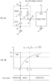
- FIG. 2A illustrates one (CR type reset circuit) of specific examples of a circuit for producing High signals and Low signals.
- a similar circuit is introduced in Stack Exchange Network, "What is benefit of diode in the RC circuit", [retrieved from the internet on January 24th, 2024], ⁇ https://electronics.stackexchange.com/questions/338078/what-is-benefit-of-diode-in-the-rc-circuit>.
- a CR type reset circuit 2 includes a resistor 21, a capacitor 22, a diode 23, a power input terminal 24, a power return terminal 25, and an output terminal 26.
- the power input terminal 24 is connected to Vcc and the power return terminal 25 is connected to the ground 12.
- the resistor 21 and the capacitor 22 are arranged in series between the power input terminal 24 and the power return terminal 25.
- the diode 23 is arranged in parallel with the resistor 21 between the power input terminal 24 and the capacitor 22.
- the diode 23 is arranged in a manner such that a cathode is on the power input terminal 24 side and an anode is on the capacitor 22 side.
- the output terminal 26 outputs a voltage of a high potential side of the capacitor 22.
- the CPU recognizes a reset port input as a High signal when the input is equal to or higher than a predetermined voltage, and as a Low signal when the input is less than the predetermined voltage.
- the CR type reset circuit 2 outputs a Low signal when 0 ⁇ t ⁇ ti and outputs a High signal when ti ⁇ t.
- Vi(t) for t ⁇ 0 in the graph in FIG. 2B represents the state where Vi became nearly equal to Vcc.
- ti needs to be equal to or greater than t d .
- time ti when V 1 becomes V T is obtained as Formula (2).
- t 1 CR log V CC V CC ⁇ V T
- log is a natural logarithm (hereinafter, the same is applied in this specification).
- Vcc and V T are values determined by specifications of the CPU, t 1 ⁇ t d is achieved by adjusting C and R.
- the denominator in the exponent (the product of C and R for the CR type reset circuit 2) of the exponential function in Formula (1) is called a "time constant" and has a dimension of "time”.
- a time constant represents characteristics of a transient response (fast or slow rise) of a CR circuit.
- Reset circuits that employs transistors to reduce power consumption are also commercially available.
- Transistors have a micro current called OFF leakage current which rapidly increases at high temperatures, and output of reset ICs fluctuates depending on the ambient temperature. Technologies have been developed to achieve a stable operation against ambient temperature change (for example, Japanese Patent Application publication gazette No. 2004-80772 ).
- CPUs are sometimes desired to be used in a high temperature environment of approximately 200°C.
- a drilling drill is equipped with a sensor that measures a position and a direction.
- a sensor control chip needs to stably operate in the environment of approximately 200°C.
- Reverse resistance of a diode can be considered to be infinite at room temperature, but the reverse resistance drops at high temperature, resulting in non-negligible leakage currents.
- V 1 t V CC 1 ⁇ e ⁇ t CR 1
- R 1 RR D R + R D Time t 2 during which V 1 rises from 0 to V T in a high temperature environment is obtained from Formula (3) and Formula (4) as the following.
- a reset circuit includes a resistor, a diode, a capacitor, a power input terminal, a power return terminal, and an output terminal which outputs a reset signal.
- the power input terminal, the resistor, the capacitor, and the power return terminal are connected in series in an order of the power input terminal, the resistor, the capacitor, and the power return terminal.
- the diode is connected in parallel with the resistor between the power input terminal and the capacitor in a manner such that a cathode is on a side closer to the power input terminal and an anode is on a side closer to the capacitor.
- the output terminal is connected to the capacitor on a side being closer to the resistor.
- a time constant of the reset circuit at the temperature T is given by CRR D (T)/(R+R D (T)).
- time during which the reset signal rises from zero volt to a reset release threshold voltage (rise time) at the temperature T is equal to or longer than specified time for the reset operation specified by the CPU.
- characteristic values, such as R D , of semiconductor encapsulated in, for example, glass or ceramic are highly reproducible in an environment of 200°C or higher, and found that an analog circuit exhibiting favorable high temperature stability can be obtained by combining a passive element using a material having favorable temperature characteristics with the encapsulated semiconductor.
- Capacitance C of a capacitor and a resistance R of a resistor are adjustable amounts in the CR type reset circuit. Hence, C and R are adjusted to obtain a CR type reset circuit whose time during which Vi rises from 0 to V T (hereinafter, referred to as "rise time") is longer than t d even at high temperature, resulting in successful reset operation.
- a CR type reset circuit 4 includes a resistor 21, a capacitor 22, a diode 23, a power input terminal 24, a power return terminal 25, and an output terminal 26. Connection between the elements is the same as the CR type reset circuit 2 described above.
- the reverse resistance R D (T) of the diode 23 at the temperature T, at which the CPU is to be operated, is first measured.
- rise time t 3 of the CR type reset circuit 4 at the temperature T is given by the following formula.
- t 3 C ′ R ′ R D T R ′ + R D T log V CC V CC ⁇ V T
- t 3 is determined by giving C' and R'.
- C' and R' of the CR type reset circuit 4 are determined so as to satisfy Formula (7) below.
- conditions of C' and R' are determined focusing only on rise time in a high temperature environment.
- conditions of C' and R' will be determined focusing on rise time at room temperature as well.
- t max ⁇ C ′ R ′ log V CC V CC ⁇ V T
- a CR type reset circuit 5 is a circuit whose C' and R' satisfy Formulas (7) and (9) and a reset circuit in which t 3 is longer than t d and t 4 is shorter than t max .
- Formula (7) can be transformed as the following. t d ⁇ C ′ R D T 1 + R D T R ′ log V CC V CC ⁇ V T ⁇ C ′ R D T log V CC V CC ⁇ V T
- C' and R' are determined by using Formulas (7) and (9) in the second embodiment, but C' and R' are determined by using Formulas (9) and (10) in the present modification.
- Both of the resistance of the resistor and the capacitance of the capacitor are adjusted so that the rise time becomes t d or longer in a high temperature environment in the first and second embodiments, while only the capacitance of the capacitor will be adjusted in a third embodiment.
- the third embodiment will be described with reference to FIGs. 6A and 6B .
- rise time ts at room temperature is expressed as Formula (11) below.
- A denotes log(V CC /(V CC -V T )).
- R is chosen to make ts ⁇ t d , a > 1.
- V C 0 , a, t d , R D (T), Vcc, and V T are known or given values.
- the capacitance C 1 can be obtained by determining b, which is 1 or greater, depending on the desired rise time.
Landscapes
- Engineering & Computer Science (AREA)
- Theoretical Computer Science (AREA)
- Physics & Mathematics (AREA)
- General Engineering & Computer Science (AREA)
- General Physics & Mathematics (AREA)
- Electronic Switches (AREA)
Abstract
Description
- The disclosed technology relates to a reset circuit which stably operates in a high temperature environment where diode leakage current is not negligible.
- For example, if a drive voltage of a central processing unit (CPU) is momentarily interrupted, internal circuits (semiconductor elements such as logic gates and memory) of the CPU malfunction, and operations do not proceed normally even if the drive voltage is restored to a normal value. In such a case, the CPU needs to be initialized. This is called reset.
- Note that, in this specification, IC chips with names such as a micro processor unit (MPU), a micro controller unit (MCU), and a digital signal processor (DSP) are also collectively referred to as CPU.
- Many CPUs have a reset port and receive a reset signal at the reset port. A reset signal is produced by a dedicated reset circuit.
FIG. 1A schematically illustrates the reset circuit and the CPU. Vcc denotes a drive voltage source (and a voltage value) of the reset circuit and the CPU, and 12 denotes ground. -
FIG. 1B schematically illustrates a relation between reset circuit output and CPU state. The CPU starts or maintains an operation state when the reset circuit output is "High", while the CPU transitions to a reset state when the reset circuit output becomes "Low". - In initializing the CPU, the CPU waits for a system clock to stabilize and initializes internal circuits and therefore, a predetermined period of time (hereinafter, denoted as td) is required for resetting. Accordingly, a "Low" signal is required to be maintained longer than td. If the "Low" signal is shorter than td, the reset fails.
-
FIG. 2A illustrates one (CR type reset circuit) of specific examples of a circuit for producing High signals and Low signals. A similar circuit is introduced in Stack Exchange Network, "What is benefit of diode in the RC circuit", [retrieved from the internet on January 24th, 2024], <https://electronics.stackexchange.com/questions/338078/what-is-benefit-of-diode-in-the-rc-circuit>. - A CR
type reset circuit 2 includes aresistor 21, acapacitor 22, adiode 23, apower input terminal 24, apower return terminal 25, and anoutput terminal 26. Thepower input terminal 24 is connected to Vcc and thepower return terminal 25 is connected to theground 12. - The
resistor 21 and thecapacitor 22 are arranged in series between thepower input terminal 24 and thepower return terminal 25. Thediode 23 is arranged in parallel with theresistor 21 between thepower input terminal 24 and thecapacitor 22. Thediode 23 is arranged in a manner such that a cathode is on thepower input terminal 24 side and an anode is on thecapacitor 22 side. Theoutput terminal 26 outputs a voltage of a high potential side of thecapacitor 22. - Assuming that the resistance of the
resistor 21 is R [Ω], the capacitance of thecapacitor 22 is C [F], and the output voltage of theoutput terminal 26 is V1 [V], when the voltage Vcc is supplied to the CRtype reset circuit 2 with capacitor charge of 0 [F] at time t = 0, an output voltage Vi on and after t = 0 is expressed by the following formula.
- The CPU recognizes a reset port input as a High signal when the input is equal to or higher than a predetermined voltage, and as a Low signal when the input is less than the predetermined voltage. Suppose the predetermined voltage is VT and ti satisfies Vi(ti) = VT, the CR
type reset circuit 2 outputs a Low signal when 0 < t < ti and outputs a High signal when ti < t. - When t is sufficiently large, Vi becomes nearly equal to Vcc. Vi(t) for t<0 in the graph in
FIG. 2B represents the state where Vi became nearly equal to Vcc. - When V1 ≈ Vcc, the
capacitor 22 is fully charged. - For resetting, Vcc of the CR
type reset circuit 2 is once set to zero. Then, the charge stored in thecapacitor 22 flows in a forward direction through thediode 23 and is quickly discharged through thepower input terminal 24. This allows the CRtype reset circuit 2 to achieve a transition from a High signal to a Low signal across t = 0. - As mentioned above, ti needs to be equal to or greater than td. From Formula (1), time ti when V1 becomes VT is obtained as Formula (2).

- Since Vcc and VT are values determined by specifications of the CPU, t1 ≥ td is achieved by adjusting C and R.
- The denominator in the exponent (the product of C and R for the CR type reset circuit 2) of the exponential function in Formula (1) is called a "time constant" and has a dimension of "time". When CR [seconds] elapses, Vi rises from zero to approximately 63% of Vcc, and when 2CR [seconds] elapses, Vi rises to approximately 86% of Vcc. Thus, a time constant represents characteristics of a transient response (fast or slow rise) of a CR circuit.
- Reset circuits (reset ICs) that employs transistors to reduce power consumption are also commercially available. Transistors have a micro current called OFF leakage current which rapidly increases at high temperatures, and output of reset ICs fluctuates depending on the ambient temperature. Technologies have been developed to achieve a stable operation against ambient temperature change (for example,
Japanese Patent Application publication gazette No. 2004-80772 - CPUs are sometimes desired to be used in a high temperature environment of approximately 200°C. For example, in drilling for shale oil, the drilling has to be performed along a shale layer that stores oil. Therefore, a drilling drill is equipped with a sensor that measures a position and a direction. In such case, a sensor control chip needs to stably operate in the environment of approximately 200°C.
- Existing reset ICs are designed to be used at 100°C or less at best, and there are no reset ICs that are guaranteed to operate at 200°C. In fact, reset ICs malfunction at temperatures as high as 200°C, being unable to withstand use at high temperatures.
- High temperature environments cause higher failure rates and shorter lifespans of electronic components. As the number of components increases, the number of components which may fail increases. Therefore, it is desirable that electronic components to be applied in high temperature environments are as simple a circuit as possible and a circuit using as simple elements as possible. In this sense, CR type reset circuits are more promising than reset ICs.
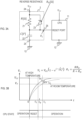
- An operation of a CR type reset circuit at high temperature will be discussed with reference to
FIGs. 3A and 3B . - Reverse resistance of a diode can be considered to be infinite at room temperature, but the reverse resistance drops at high temperature, resulting in non-negligible leakage currents.
- When the reverse resistance of the
diode 23 is denoted as RD [Ω], the output voltage of theoutput terminal 26 is expressed as the following.


- When R/RD is negligibly small, t2 = t1 is satisfied. As RD decreases (as an operating environment becomes hotter), t2 becomes shorter. When t2 becomes shorter than td, reset fails.
- It is desirable that a diode with low leakage current (large RD) even at high temperature can be used, but diodes which maintain a sufficient reverse resistance at 200°C are not generally available at present.
- To solve the above described problems, a reset circuit according to the disclosed technology includes a resistor, a diode, a capacitor, a power input terminal, a power return terminal, and an output terminal which outputs a reset signal.
- The power input terminal, the resistor, the capacitor, and the power return terminal are connected in series in an order of the power input terminal, the resistor, the capacitor, and the power return terminal.
- The diode is connected in parallel with the resistor between the power input terminal and the capacitor in a manner such that a cathode is on a side closer to the power input terminal and an anode is on a side closer to the capacitor.
- The output terminal is connected to the capacitor on a side being closer to the resistor.
- When a high temperature at which the reset circuit is operated is denoted as T, a reverse resistance of the diode at the temperature T is denoted as RD(T), a resistance of the resistor is denoted as R, and capacitance of the capacitor is denoted as C, a time constant of the reset circuit at the temperature T is given by CRRD(T)/(R+RD(T)).
- Regarding the output signal of the reset circuit, time during which the reset signal rises from zero volt to a reset release threshold voltage (rise time) at the temperature T is equal to or longer than specified time for the reset operation specified by the CPU.
- According to the reset circuit of the disclosed technology, a reset circuit which operates at high temperature with low failure rate can be realized.
-
-
FIG. 1A schematically illustrates a reset circuit and a CPU to be reset. -
FIG. 1B schematically illustrates a relation between reset circuit output and CPU state. -
FIG. 2A is a diagram for explaining a configuration of a CR type reset circuit. -
FIG. 2B is a diagram for explaining an output signal of a CR type reset circuit. -
FIG. 3A is a diagram showing resistance which cause problems at high temperature. -
FIG. 3B is a diagram for explaining a problem of an operation of a CR type reset circuit at high temperature. -
FIG. 4A is a diagram for explaining a configuration of a reset circuit according to a first embodiment. -
FIG. 4B is a diagram for explaining a method for designing the reset circuit according to the first embodiment. -
FIG. 5A is a diagram for explaining a configuration of a reset circuit according to a second embodiment. -
FIG. 5B is a diagram for explaining a method for designing the reset circuit according to the second embodiment. -
FIG. 6A is a diagram for explaining a configuration of a reset circuit according to a third embodiment. -
FIG. 6B is a diagram for explaining a method for designing the reset circuit according to the third embodiment. - Embodiments according to the disclosed technology will be described in detail below. Here, components having the same functions will be provided with the same reference characters and the repeated description thereof will be omitted.
- The inventors of the present application found that characteristic values, such as RD, of semiconductor encapsulated in, for example, glass or ceramic are highly reproducible in an environment of 200°C or higher, and found that an analog circuit exhibiting favorable high temperature stability can be obtained by combining a passive element using a material having favorable temperature characteristics with the encapsulated semiconductor. Capacitance C of a capacitor and a resistance R of a resistor are adjustable amounts in the CR type reset circuit. Hence, C and R are adjusted to obtain a CR type reset circuit whose time during which Vi rises from 0 to VT (hereinafter, referred to as "rise time") is longer than td even at high temperature, resulting in successful reset operation.
- This will be described with reference to
FIGs. 4A and 4B . A CR type resetcircuit 4 includes aresistor 21, acapacitor 22, adiode 23, apower input terminal 24, apower return terminal 25, and anoutput terminal 26. Connection between the elements is the same as the CR type resetcircuit 2 described above. - The reverse resistance RD(T) of the
diode 23 at the temperature T, at which the CPU is to be operated, is first measured. - Subsequently, a resistance R' of the
resistor 21 and capacitance C' of thecapacitor 22 are determined. - Based on Formula (5), rise time t3 of the CR type reset
circuit 4 at the temperature T is given by the following formula.
- Since Vcc and VT are specified values and RD(T) is a measured value, t3 is determined by giving C' and R'. C' and R' of the CR type reset
circuit 4 are determined so as to satisfy Formula (7) below.
- As a result, the CR type reset
circuit 4 in which t3 is longer than td can be obtained. - This is the description of the first embodiment.
- In the first embodiment, the conditions of C' and R' are determined focusing only on rise time in a high temperature environment. In a second embodiment, conditions of C' and R' will be determined focusing on rise time at room temperature as well.
- This will be described with reference to
FIGs. 5A and 5B . - Rise time t4 when the CR type reset
circuit 4 of the first embodiment is operated at room temperature is given by Formula (8) below.
- For some applications, too long rise time (time required for resetting) is not acceptable. Accordingly, a rise time tolerable limit tmax at room temperature is determined so as to limit ranges of C' and R'. Its condition is given by Formula (9).

- In summary, a CR type reset
circuit 5 according to the second embodiment is a circuit whose C' and R' satisfy Formulas (7) and (9) and a reset circuit in which t3 is longer than td and t4 is shorter than tmax. - This is the description of the second embodiment.
- [Modification of second embodiment]
- Assuming that R' is determined to be larger than RD(T), Formula (7) can be transformed as the following.

- C' and R' are determined by using Formulas (7) and (9) in the second embodiment, but C' and R' are determined by using Formulas (9) and (10) in the present modification.
- What is determined by Formula (10) is only C'. Once C' is determined, only R' needs to be determined by Formula (9). This facilitates the design of C' and R'.
- This is the description of the modification of the second embodiment.
- Both of the resistance of the resistor and the capacitance of the capacitor are adjusted so that the rise time becomes td or longer in a high temperature environment in the first and second embodiments, while only the capacitance of the capacitor will be adjusted in a third embodiment.
- Specifically, for a CR type reset circuit which realizes td or longer rise time at room temperature, only C is changed while R is kept fixed.
- The third embodiment will be described with reference to
FIGs. 6A and 6B . - When a resistance of the
resistor 21 is denoted as R and capacitance of thecapacitor 22 before change is denoted as Co, rise time ts at room temperature is expressed as Formula (11) below.
- When a reverse resistance of the diode at the temperature T is denoted as RD(T), rise time t6 at the temperature T is expressed as Formula (12) below.

- Suppose the capacitance of the
capacitor 22 is changed to C1 and rise time t7 ≥ td at the temperature T is obtained.


- Meaning of Formula (15) is as follows.
- C0, a, td, RD(T), Vcc, and VT are known or given values.
- In a CR type reset
circuit 6 having C1 obtained based on b = 1, the rise time at high temperature is exactly td. - That is, the capacitance C1 can be obtained by determining b, which is 1 or greater, depending on the desired rise time.
- This is the description of the third embodiment.
- The foregoing description of the embodiments of the invention has been presented for the purpose of illustration and description. It is not intended to be exhaustive and to limit the invention to the precise form disclosed. Modifications or variations are possible in light of the above teaching. The embodiment was chosen and described to provide the best illustration of the principles of the invention and its practical application, and to enable those of ordinary skill in the art to utilize the invention in various embodiments and with various modifications as are suited to the particular use contemplated. All such modifications and variations are within the scope of the invention as determined by the appended claims when interpreted in accordance with the breadth to which they are fairly, legally, and equitably entitled.
Claims (8)
- A method for designing a reset circuit which outputs a reset signal to a CPU in a high temperature environment,the reset circuit including a resistor, a diode, a capacitor, a power input terminal, a power return terminal, and an output terminal which outputs a reset signal,the power input terminal, the resistor, the capacitor, and the power return terminal being connected in series in an order of the power input terminal, the resistor, the capacitor, and the power return terminal,the diode being connected in parallel with the resistor between the power input terminal and the capacitor in a manner such that a cathode is on a side closer to the power input terminal and an anode is on a side closer to the capacitor, andthe output terminal being connected to the capacitor on a side being closer to the resistor,the method comprising:measuring a reverse resistance RD(T) of the diode at high temperature T, at which the reset circuit is operated;obtaining specified time td for a reset operation, the specified time td being specified by the CPU, a drive voltage Vcc of the reset circuit, and a reset release voltage VT; anddetermining capacitance C of the capacitor and a resistance R of the resistor so that the capacitance C and the resistance R satisfy a following formula:

- The method for designing a reset circuit according to Claim 1, whereina maximum tolerable value of rise time of the reset circuit at room temperature is denoted as tmax, andthe capacitance C of the capacitor and the resistance R of the resistor are determined to further satisfy a following formula:

- The method for designing a reset circuit according to Claim 2, wherein
the capacitance C of the capacitor and the resistance R of the resistor are determined by replacing a following formula:

- A method for designing a reset circuit which outputs a reset signal to a CPU in a high temperature environment,the reset circuit including a resistor, a diode, a capacitor, a power input terminal, a power return terminal, and an output terminal which outputs a reset signal,the power input terminal, the resistor, the capacitor, and the power return terminal being connected in series in an order of the power input terminal, the resistor, the capacitor, and the power return terminal,the diode being connected in parallel with the resistor between the power input terminal and the capacitor in a manner such that a cathode is on a side closer to the power input terminal and an anode is on a side closer to the capacitor, andthe output terminal being connected to the capacitor on a side being closer to the resistor,the method comprising:obtaining specified time td for a reset operation, the specified time td being specified by the CPU, a drive voltage Vcc of the reset circuit, and a reset release voltage VT;setting a value of the resistor so as to obtain 1 or greater of value a, the value a being obtained by dividing time, during which the reset signal rises from zero volt to VT when capacitance of the capacitor is set to C0 and the reset circuit is operated at room temperature, by td;measuring a reverse resistance RD(T) of the diode at high temperature T, at which the reset circuit is operated; andsetting the capacitance of the capacitor to following C1 or greater:

- A reset circuit which outputs a reset signal to a CPU in a high temperature environment, the reset circuit comprising:a resistor; a diode; a capacitor; a power input terminal; a power return terminal; and an output terminal which outputs a reset signal, whereinthe power input terminal, the resistor, the capacitor, and the power return terminal are connected in series in an order of the power input terminal, the resistor, the capacitor, and the power return terminal,the diode is connected in parallel with the resistor between the power input terminal and the capacitor in a manner such that a cathode is on a side closer to the power input terminal and an anode is on a side closer to the capacitor,the output terminal is connected to the capacitor on a side being closer to the resistor,when a reverse resistance of the diode at high temperature T, at which the reset circuit is operated, is denoted as RD(T), a resistance of the resistor is denoted as R, and capacitance of the capacitor is denoted as C, a time constant of the reset circuit at the high temperature T is given by a following formula:
 time during which the reset signal rises from zero volt to a reset release threshold voltage at the high temperature T, the time being referred to as rise time, is equal to or longer than specified time for a reset operation, the specified time being specified by the CPU.
- The reset circuit according to Claim 5, whereina time constant of the reset circuit at room temperature is given by a product of the C and the R, andthe capacitance C of the capacitor and the resistance R of the resistor are determined so that time, during which the reset signal rises from zero volt to a reset release threshold voltage at room temperature, is predetermined time or shorter.
- The reset circuit according to Claim 6, wherein
a time constant of the reset circuit at the high temperature T is approximated to be a product of the C and the RD(T) so as to determine the capacitance C of the capacitor and the resistance R. - A reset circuit which outputs a reset signal to a CPU in a high temperature environment, the reset circuit comprising:a resistor; a diode; a capacitor; a power input terminal; a power return terminal; and an output terminal which outputs a reset signal, whereinthe power input terminal, the resistor, the capacitor, and the power return terminal are connected in series in an order of the power input terminal, the resistor, the capacitor, and the power return terminal,the diode is connected in parallel with the resistor between the power input terminal and the capacitor in a manner such that a cathode is on a side closer to the power input terminal and an anode is on a side closer to the capacitor,the output terminal is connected to the capacitor on a side being closer to the resistor,in an operation at room temperature with capacitance of the capacitor set to C0, where a reverse resistance of the diode at high temperature T, at which the reset circuit is operated, is denoted as RD(T), specified time for a reset operation, the specified time being specified by the CPU, is denoted as td, a drive voltage of the reset circuit is denoted as Vcc, and a reset release voltage is denoted as VT, when time during which the reset signal rises from zero volt to VT is ata (a ≥ 1), the capacitance of the capacitor is set to be equal to or greater than following Ci:

Applications Claiming Priority (1)
| Application Number | Priority Date | Filing Date | Title |
|---|---|---|---|
| JP2023134102A JP2025029444A (en) | 2023-08-21 | 2023-08-21 | Reset circuit and reset circuit design method |
Publications (2)
| Publication Number | Publication Date |
|---|---|
| EP4513756A1 true EP4513756A1 (en) | 2025-02-26 |
| EP4513756B1 EP4513756B1 (en) | 2025-12-31 |
Family
ID=91959393
Family Applications (1)
| Application Number | Title | Priority Date | Filing Date |
|---|---|---|---|
| EP24189597.8A Active EP4513756B1 (en) | 2023-08-21 | 2024-07-18 | RESET CIRCUIT AND METHOD FOR DESIGNING A RESET CIRCUIT |
Country Status (3)
| Country | Link |
|---|---|
| US (1) | US12591282B2 (en) |
| EP (1) | EP4513756B1 (en) |
| JP (1) | JP2025029444A (en) |
Citations (3)
| Publication number | Priority date | Publication date | Assignee | Title |
|---|---|---|---|---|
| JPH0926835A (en) * | 1995-07-10 | 1997-01-28 | Sanyo Electric Co Ltd | Reset circuit |
| JP2004080772A (en) | 2002-08-20 | 2004-03-11 | Samsung Electronics Co Ltd | Power-on reset circuit and method |
| US20070103211A1 (en) * | 2005-11-04 | 2007-05-10 | Hon Hai Precision Industry Co., Ltd. | Reset circuit |
Family Cites Families (5)
| Publication number | Priority date | Publication date | Assignee | Title |
|---|---|---|---|---|
| NL244911A (en) * | 1959-10-30 | |||
| JPS5932024A (en) * | 1982-08-13 | 1984-02-21 | Hitachi Ltd | semiconductor integrated circuit |
| US4520418A (en) * | 1983-04-25 | 1985-05-28 | Susi Roger E | Reset circuit |
| JPS60212028A (en) * | 1984-04-05 | 1985-10-24 | Mitsubishi Electric Corp | Reset circuit |
| US8671288B2 (en) * | 2010-12-21 | 2014-03-11 | Advanced Micro Devices, Inc. | Processor with power control via instruction issuance |
-
2023
- 2023-08-21 JP JP2023134102A patent/JP2025029444A/en active Pending
-
2024
- 2024-06-28 US US18/758,501 patent/US12591282B2/en active Active
- 2024-07-18 EP EP24189597.8A patent/EP4513756B1/en active Active
Patent Citations (3)
| Publication number | Priority date | Publication date | Assignee | Title |
|---|---|---|---|---|
| JPH0926835A (en) * | 1995-07-10 | 1997-01-28 | Sanyo Electric Co Ltd | Reset circuit |
| JP2004080772A (en) | 2002-08-20 | 2004-03-11 | Samsung Electronics Co Ltd | Power-on reset circuit and method |
| US20070103211A1 (en) * | 2005-11-04 | 2007-05-10 | Hon Hai Precision Industry Co., Ltd. | Reset circuit |
Also Published As
| Publication number | Publication date |
|---|---|
| US20250068218A1 (en) | 2025-02-27 |
| EP4513756B1 (en) | 2025-12-31 |
| US12591282B2 (en) | 2026-03-31 |
| JP2025029444A (en) | 2025-03-06 |
Similar Documents
| Publication | Publication Date | Title |
|---|---|---|
| US6695475B2 (en) | Temperature sensing circuit and method | |
| JP4279825B2 (en) | Integrated circuit die with temperature detection circuit and temperature detection circuit calibration system and method | |
| US8061895B2 (en) | Semiconductor device | |
| US7199623B2 (en) | Method and apparatus for providing a power-on reset signal | |
| US7695189B2 (en) | System to calibrate on-die temperature sensor | |
| US7038482B1 (en) | Circuit and method for automatic measurement and compensation of transistor threshold voltage mismatch | |
| US20170187358A1 (en) | Semiconductor device | |
| US10262985B2 (en) | Circuits and methods for lowering leakage in ultra-low-power MOS integrated circuits | |
| KR970008141B1 (en) | Burn-in Circuit of Semiconductor Device | |
| EP3893079B1 (en) | In-chip reference current generation circuit | |
| US10147721B1 (en) | Method and apparatus for dynamic calibration of on-die-precision-resistors | |
| TWI301976B (en) | Internal voltage generating circuit in semiconductor memory device | |
| US12591282B2 (en) | Reset circuit and method for designing reset circuit | |
| US9312850B2 (en) | Testable power-on-reset circuit | |
| US6590405B2 (en) | CMOS integrated circuit and timing signal generator using same | |
| EP1612635B1 (en) | Short-circuit detection with current-mirror | |
| TW293910B (en) | ||
| US8179729B2 (en) | Memory circuit and voltage detection circuit including the same | |
| CN114911298A (en) | Over-temperature protection circuit and test method thereof | |
| US7286020B1 (en) | Techniques for monitoring and replacing circuits to maintain high performance | |
| KR100845773B1 (en) | Power-up signal trip point measuring circuit of semiconductor memory device and power-up signal trip point level measuring method using same | |
| US7627839B1 (en) | Process corner indicator and estimation circuit | |
| TW202441344A (en) | Apparatus comprising a bias current generator | |
| US20030227809A1 (en) | Temperature-adjusted pre-charged reference for an integrated circuit 1T/1C ferroelectric memory | |
| US7634746B1 (en) | Process corner estimation circuit with temperature compensation |
Legal Events
| Date | Code | Title | Description |
|---|---|---|---|
| PUAI | Public reference made under article 153(3) epc to a published international application that has entered the european phase |
Free format text: ORIGINAL CODE: 0009012 |
|
| STAA | Information on the status of an ep patent application or granted ep patent |
Free format text: STATUS: THE APPLICATION HAS BEEN PUBLISHED |
|
| AK | Designated contracting states |
Kind code of ref document: A1 Designated state(s): AL AT BE BG CH CY CZ DE DK EE ES FI FR GB GR HR HU IE IS IT LI LT LU LV MC ME MK MT NL NO PL PT RO RS SE SI SK SM TR |
|
| STAA | Information on the status of an ep patent application or granted ep patent |
Free format text: STATUS: REQUEST FOR EXAMINATION WAS MADE |
|
| 17P | Request for examination filed |
Effective date: 20250512 |
|
| RIC1 | Information provided on ipc code assigned before grant |
Ipc: H03K 17/22 20060101AFI20250707BHEP Ipc: G06F 1/24 20060101ALI20250707BHEP |
|
| GRAP | Despatch of communication of intention to grant a patent |
Free format text: ORIGINAL CODE: EPIDOSNIGR1 |
|
| STAA | Information on the status of an ep patent application or granted ep patent |
Free format text: STATUS: GRANT OF PATENT IS INTENDED |
|
| INTG | Intention to grant announced |
Effective date: 20250909 |
|
| GRAS | Grant fee paid |
Free format text: ORIGINAL CODE: EPIDOSNIGR3 |
|
| GRAA | (expected) grant |
Free format text: ORIGINAL CODE: 0009210 |
|
| STAA | Information on the status of an ep patent application or granted ep patent |
Free format text: STATUS: THE PATENT HAS BEEN GRANTED |
|
| AK | Designated contracting states |
Kind code of ref document: B1 Designated state(s): AL AT BE BG CH CY CZ DE DK EE ES FI FR GB GR HR HU IE IS IT LI LT LU LV MC ME MK MT NL NO PL PT RO RS SE SI SK SM TR |
|
| REG | Reference to a national code |
Ref country code: CH Ref legal event code: F10 Free format text: ST27 STATUS EVENT CODE: U-0-0-F10-F00 (AS PROVIDED BY THE NATIONAL OFFICE) Effective date: 20251231 Ref country code: GB Ref legal event code: FG4D |
|
| REG | Reference to a national code |
Ref country code: DE Ref legal event code: R096 Ref document number: 602024001923 Country of ref document: DE |
|
| REG | Reference to a national code |
Ref country code: IE Ref legal event code: FG4D |
|
| REG | Reference to a national code |
Ref country code: LT Ref legal event code: MG9D |
|
| PG25 | Lapsed in a contracting state [announced via postgrant information from national office to epo] |
Ref country code: NO Free format text: LAPSE BECAUSE OF FAILURE TO SUBMIT A TRANSLATION OF THE DESCRIPTION OR TO PAY THE FEE WITHIN THE PRESCRIBED TIME-LIMIT Effective date: 20260331 |
|
| PG25 | Lapsed in a contracting state [announced via postgrant information from national office to epo] |
Ref country code: FI Free format text: LAPSE BECAUSE OF FAILURE TO SUBMIT A TRANSLATION OF THE DESCRIPTION OR TO PAY THE FEE WITHIN THE PRESCRIBED TIME-LIMIT Effective date: 20251231 Ref country code: HR Free format text: LAPSE BECAUSE OF FAILURE TO SUBMIT A TRANSLATION OF THE DESCRIPTION OR TO PAY THE FEE WITHIN THE PRESCRIBED TIME-LIMIT Effective date: 20251231 |
|
| PG25 | Lapsed in a contracting state [announced via postgrant information from national office to epo] |
Ref country code: RS Free format text: LAPSE BECAUSE OF FAILURE TO SUBMIT A TRANSLATION OF THE DESCRIPTION OR TO PAY THE FEE WITHIN THE PRESCRIBED TIME-LIMIT Effective date: 20260331 |
|
| PG25 | Lapsed in a contracting state [announced via postgrant information from national office to epo] |
Ref country code: LV Free format text: LAPSE BECAUSE OF FAILURE TO SUBMIT A TRANSLATION OF THE DESCRIPTION OR TO PAY THE FEE WITHIN THE PRESCRIBED TIME-LIMIT Effective date: 20251231 |
|
| PG25 | Lapsed in a contracting state [announced via postgrant information from national office to epo] |
Ref country code: BG Free format text: LAPSE BECAUSE OF FAILURE TO SUBMIT A TRANSLATION OF THE DESCRIPTION OR TO PAY THE FEE WITHIN THE PRESCRIBED TIME-LIMIT Effective date: 20251231 |
|
| REG | Reference to a national code |
Ref country code: NL Ref legal event code: MP Effective date: 20251231 |
|
| REG | Reference to a national code |
Ref country code: AT Ref legal event code: MK05 Ref document number: 1874612 Country of ref document: AT Kind code of ref document: T Effective date: 20251231 |
|
| PG25 | Lapsed in a contracting state [announced via postgrant information from national office to epo] |
Ref country code: NL Free format text: LAPSE BECAUSE OF FAILURE TO SUBMIT A TRANSLATION OF THE DESCRIPTION OR TO PAY THE FEE WITHIN THE PRESCRIBED TIME-LIMIT Effective date: 20251231 |
|
| PG25 | Lapsed in a contracting state [announced via postgrant information from national office to epo] |
Ref country code: LT Free format text: LAPSE BECAUSE OF FAILURE TO SUBMIT A TRANSLATION OF THE DESCRIPTION OR TO PAY THE FEE WITHIN THE PRESCRIBED TIME-LIMIT Effective date: 20251231 |
|
| PG25 | Lapsed in a contracting state [announced via postgrant information from national office to epo] |
Ref country code: SM Free format text: LAPSE BECAUSE OF FAILURE TO SUBMIT A TRANSLATION OF THE DESCRIPTION OR TO PAY THE FEE WITHIN THE PRESCRIBED TIME-LIMIT Effective date: 20251231 |
|
| PG25 | Lapsed in a contracting state [announced via postgrant information from national office to epo] |
Ref country code: ES Free format text: LAPSE BECAUSE OF FAILURE TO SUBMIT A TRANSLATION OF THE DESCRIPTION OR TO PAY THE FEE WITHIN THE PRESCRIBED TIME-LIMIT Effective date: 20251231 |
|
| PG25 | Lapsed in a contracting state [announced via postgrant information from national office to epo] |
Ref country code: PL Free format text: LAPSE BECAUSE OF FAILURE TO SUBMIT A TRANSLATION OF THE DESCRIPTION OR TO PAY THE FEE WITHIN THE PRESCRIBED TIME-LIMIT Effective date: 20251231 |
|
| PG25 | Lapsed in a contracting state [announced via postgrant information from national office to epo] |
Ref country code: IT Free format text: LAPSE BECAUSE OF FAILURE TO SUBMIT A TRANSLATION OF THE DESCRIPTION OR TO PAY THE FEE WITHIN THE PRESCRIBED TIME-LIMIT Effective date: 20251231 |
|
| PG25 | Lapsed in a contracting state [announced via postgrant information from national office to epo] |
Ref country code: AT Free format text: LAPSE BECAUSE OF FAILURE TO SUBMIT A TRANSLATION OF THE DESCRIPTION OR TO PAY THE FEE WITHIN THE PRESCRIBED TIME-LIMIT Effective date: 20251231 |
|
| PG25 | Lapsed in a contracting state [announced via postgrant information from national office to epo] |
Ref country code: EE Free format text: LAPSE BECAUSE OF FAILURE TO SUBMIT A TRANSLATION OF THE DESCRIPTION OR TO PAY THE FEE WITHIN THE PRESCRIBED TIME-LIMIT Effective date: 20251231 |
|
| PG25 | Lapsed in a contracting state [announced via postgrant information from national office to epo] |
Ref country code: PT Free format text: LAPSE BECAUSE OF FAILURE TO SUBMIT A TRANSLATION OF THE DESCRIPTION OR TO PAY THE FEE WITHIN THE PRESCRIBED TIME-LIMIT Effective date: 20260430 Ref country code: IS Free format text: LAPSE BECAUSE OF FAILURE TO SUBMIT A TRANSLATION OF THE DESCRIPTION OR TO PAY THE FEE WITHIN THE PRESCRIBED TIME-LIMIT Effective date: 20260430 |
|
| PG25 | Lapsed in a contracting state [announced via postgrant information from national office to epo] |
Ref country code: CZ Free format text: LAPSE BECAUSE OF FAILURE TO SUBMIT A TRANSLATION OF THE DESCRIPTION OR TO PAY THE FEE WITHIN THE PRESCRIBED TIME-LIMIT Effective date: 20251231 |
|
| PG25 | Lapsed in a contracting state [announced via postgrant information from national office to epo] |
Ref country code: SK Free format text: LAPSE BECAUSE OF FAILURE TO SUBMIT A TRANSLATION OF THE DESCRIPTION OR TO PAY THE FEE WITHIN THE PRESCRIBED TIME-LIMIT Effective date: 20251231 |
|
| PG25 | Lapsed in a contracting state [announced via postgrant information from national office to epo] |
Ref country code: SE Free format text: LAPSE BECAUSE OF FAILURE TO SUBMIT A TRANSLATION OF THE DESCRIPTION OR TO PAY THE FEE WITHIN THE PRESCRIBED TIME-LIMIT Effective date: 20251231 |