EP4513548A1 - Electronic component and arrangement - Google Patents
Electronic component and arrangement Download PDFInfo
- Publication number
- EP4513548A1 EP4513548A1 EP23192683.3A EP23192683A EP4513548A1 EP 4513548 A1 EP4513548 A1 EP 4513548A1 EP 23192683 A EP23192683 A EP 23192683A EP 4513548 A1 EP4513548 A1 EP 4513548A1
- Authority
- EP
- European Patent Office
- Prior art keywords
- package
- electronic
- electronic component
- recess
- component according
- Prior art date
- Legal status (The legal status is an assumption and is not a legal conclusion. Google has not performed a legal analysis and makes no representation as to the accuracy of the status listed.)
- Pending
Links
Images


Classifications
-
- H—ELECTRICITY
- H10—SEMICONDUCTOR DEVICES; ELECTRIC SOLID-STATE DEVICES NOT OTHERWISE PROVIDED FOR
- H10W—GENERIC PACKAGES, INTERCONNECTIONS, CONNECTORS OR OTHER CONSTRUCTIONAL DETAILS OF DEVICES COVERED BY CLASS H10
- H10W74/00—Encapsulations, e.g. protective coatings
- H10W74/10—Encapsulations, e.g. protective coatings characterised by their shape or disposition
- H10W74/111—Encapsulations, e.g. protective coatings characterised by their shape or disposition the semiconductor body being completely enclosed
-
- H—ELECTRICITY
- H10—SEMICONDUCTOR DEVICES; ELECTRIC SOLID-STATE DEVICES NOT OTHERWISE PROVIDED FOR
- H10W—GENERIC PACKAGES, INTERCONNECTIONS, CONNECTORS OR OTHER CONSTRUCTIONAL DETAILS OF DEVICES COVERED BY CLASS H10
- H10W76/00—Containers; Fillings or auxiliary members therefor; Seals
- H10W76/10—Containers or parts thereof
- H10W76/12—Containers or parts thereof characterised by their shape
-
- H—ELECTRICITY
- H10—SEMICONDUCTOR DEVICES; ELECTRIC SOLID-STATE DEVICES NOT OTHERWISE PROVIDED FOR
- H10W—GENERIC PACKAGES, INTERCONNECTIONS, CONNECTORS OR OTHER CONSTRUCTIONAL DETAILS OF DEVICES COVERED BY CLASS H10
- H10W90/00—Package configurations
Definitions
- This disclosure relates to electronic components, and particularly to the component packaging which surrounds electronic chips.
- Electronic chips which may also be called dies, are usually prepared by manufacturing various electronic structures on a substrate and cutting the substrate into small, chip-size pieces. Each chip can then be placed inside a protective package which forms an enclosure where the chip is protected from the surrounding environment. The chip can be mechanically attached to a support structure inside the enclosure, such as a die pad, and electrically connected to contacts which extend outside of the enclosure. The packaged chip thereby forms an electronic component which can be mounted on a circuit board.
- An object of the present disclosure is to provide a new apparatus.
- the disclosure is based on the idea of designing the side of the electronic component configured to be provided towards a printed circuit board (PCB) to provide space between the electronic component and the printed circuit board for at least one discrete component. This enables saving use of effective area of the printed circuit board.
- PCB printed circuit board
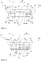
- Figure 1 illustrates an electronic component 1 according to an embodiment schematically seen from a first side
- Figure 2 illustrates the embodiment of Figure 1 schematically seen from a second side
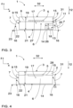
- Figure 3 illustrates an electronic component according to another embodiment schematically seen from a first side
- Figure 4 illustrates the embodiment of Figure 3 schematically seen from the first side in cross section
- Figure 5 illustrates an electronic component according to a further embodiment schematically seen from a first side
- Figure 6 illustrates an electronic component according to a further embodiment schematically seen from a first side
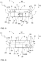
- Figures 7-9 illustrate electronic components according to different embodiments schematically seen from the bottom side.
- the plane defined by the x- and y-axes is parallel to the plane of a printed circuit board (PCB), later called a circuit board in this disclosure, to which the electronic component is configured to be attached.
- PCB printed circuit board
- the direction defined by the z-axis is perpendicular to the same plane of the circuit board, or a circuit board plane.
- the words “bottom” and “top” only refer to how the component is configured to be placed with respect to the circuit board.
- the bottom side of the component is configured to be attached to the surface of the circuit board.
- Words such as “above” and “below” are used with the same meaning - a first part which is below a second part is configured to be closer to the circuit board, and the second part is provided on the top side of the component with respect to the first part.
- Figures 1 and 3-6 show different embodiments of the electronic component in the direction of the y-axis
- Figure 2 shows an embodiment of the electronic component in the direction of the x-axis
- Figures 7-9 show embodiments of the electronic component in the direction of z-axis.
- the electronic component 1 comprises a package 2 with a top side 3 and a bottom side 4, at least one electronic chip 5, also called a chip 5 in this disclosure, housed within an enclosure 6 inside the package 2.
- the package 2 may further comprise, besides the top side 3 and the bottom side 4, four sides: first side 8, second side 9, third side 10 and a fourth side 11.
- the package 2 further comprises a plurality of electronic leads 7 protruding from the package 2 and configured to extend from at least two sides, preferably from at least two opposite sides of the package, such as the second side 9 and the fourth side 11 of the package 2 as seen in Figures 1 and 3-6 , at least in a first direction 12 extending from the top side 3 of the package 2 towards the bottom side 4 of the package 2.
- the electronic leads 7 are configured to protrude from the package 2 at least in a direction corresponding to a downward direction.
- the electronic leads 7 are configured to protrude from the package 2 at least towards the side configured to be facing a circuit board 40, when the electronic component 1 is attached to the circuit board 40.
- the electronic leads 7 may further be configured to extend outwards from the package 2, for instance in a bended manner, such as seen in Figure 1 and 3-6 .
- the package 2 comprises on the bottom side 4 of the package 2 at least one recess 13.
- the recess 13 is provided within an area 14 defined by outer edges 15, 16 of the package 2 and/or the electronic leads 7. More particularly, the recess 13 is provided within an area 14 defined by outer edges 15, 16 of the package 2 and/or the electronic leads 7, whichever is further from the centre 17 of the package 2.
- the outer edges 15 of the package 2 refer to the edges of the package 2 that are farthest from a centre 17 of the package 2 in the x-y-plane, in other words on the first side 8, the second side 9, the third side 10 and the fourth side 11.
- the outer edges 16 of the electronic leads 7 refer to the package side edges of the portions of electronic leads 7 farthest from the centre 17 of the package 2 in the direction extending from the top side 3 of the package 2 towards the bottom side 4 of the package 2.
- the edges of this portion on the side facing towards the package 2 defines the outer edge 16 of the electronic lead 7 for its part defining the area 14.
- the centre 17 of the package 2 refers to a centre point measured from the farthest points of the package 2 in the directions of x-, y- and z-axes.
- the electronic leads 7 can be used to make electric connections to the electronic chips 5 from an outside of the package 2.
- the electronic chips 5 may be connected to the electronic leads 7 inside the package 2, for example by wire bonding or flip chip bonding (not shown), and the electronic leads 7 may extend outward from the package 2 in a side direction which is substantially perpendicular to the z-axis. Electric connections to the electronic chips 5 can then be made by connecting the electronic leads 5 to suitable connectors.
- the electronic lead 7 may be configured to extend outwards from the package 2 in a bended manner in such a way that a first portion of the electronic lead 7 extends from an outer edge 15 of the package 2 in a direction perpendicular to the side 8, 9, 10, 11, on which the electronic lead 7 protrudes from, that a second portion of the electronic lead 7 extends in the first direction 12 between a first bend 31 and the outer edge 16 of the electronic lead 7, and that a third portion extends in a direction parallel to the first portion starting at a second ben at the outer edge 16 of the electronic lead 7.
- the second portion of the electronic lead 7 may extend in a direction perpendicular to the first portion, as shown in Figures 4 and 6 .
- the second portion of the electronic lead 7 may extend in an outwards angled manner with respect to the first portion, as shown in Figures 1 , 3 , 5 , 10 and 11 .
- the recess 13 extends at least from the bottom side 4 towards the top side 3 of the package 2.
- the top side 3 refers to a plane parallel to the plane of the circuit board, to which the electronic component is configured to be attached, comprising the highest point of the package 2 with respect to the plane of the circuit board.
- the top side 3 refers to a plane parallel to a plane 21 defined by bottom surfaces 23 of the electronic leads 7 comprising the highest point of the package 2 with respect to the plane defined by bottom surfaces 23 of the electronic leads 7.
- a width 26 of the recess 13 is measured in a second direction 32 extending from one side 8, 9, 10, 22 of the package 2 provided with electronic leads 7 towards an opposite side 8, 9, 10, 11 of the package 2.
- a width 26 of the recess 13 measured in a second direction 32 extending from one side 8, 9, 10, 22 of the package 2 provided with electronic leads 7 towards an opposite side 8, 9, 10, 11 of the package 2 is in the range of 10 to 100 percent of a width 27 of the package 2.
- the width 27 of the package 2 refers to the distance between the furthest points of the package 2 in the direction of the x-axis.
- a length 24 of the recess 13 is measured in a third direction 33, which is a direction perpendicular to the first direction 12 and the second direction 32.
- a length 24 of the recess 13 measured in a third direction 33 which is a direction perpendicular to the first direction 12 and the second direction 32, is in the range of 10 to 100 percent of a length 25 of the package 2.
- the length 25 of the package 2 refers to the distance between the furthest points of the package 2 in the direction of the y-axis.
- the recess 13 is configured to define within the area 14, in other words upwards or towards the package 2 from the area 14, a space 20 between the package 2 and a plane 21 defined by bottom surfaces 23 of the electronic leads 7, more particularly a space 20 defined by the recess 13, the inner surfaces 22 of the electronic leads 7 and the plane 21 defined by bottom surfaces 23 of the electronic leads 7.
- the space 20 is, thus, also limited by planes from the sides 8, 9, 10, 11 towards the area 14, more particularly extending in the direction of the z-axis, on sides 8, 9, 10, 11 which are not provided with electronic leads 7.
- the space 20 is designed to receive at least one discrete component 41.
- the space 20 may be dimensioned to receive the at least one discrete component 41 within the space 20.
- Discrete components 41 are components used in connection with circuit boards 40, which comprise a single component or electrical device, as opposed to for instance integrated circuit packages comprising multiple components contained in a single package.
- a discrete component 41 can be provided as a through-hole package or a surface mount device (SMD).
- the discrete component 41 may comprise a passive component, in other words a component that doesn't generate power or electrical energy.
- the discrete component 41 may comprise an active component.
- the recess 13 is provided at least on one side 8, 9, 10, 11 of the package 2 and extends to an outer edge 15 of the package 2 at least on that side 8, 9, 10, 11.
- the recess 13 may open at least to the side 8, 9, 10, 11 on which it is provided, such as in the embodiments of Figures 1-11 .
- the recess 13 extends to an outer edge 15 of the package 2 at least on two adjacent sides 8, 9, 10, 11, such as on the first side 8 and the second side 9 or on the first side 8 and the fourth side 11 of the package 2, such as in embodiments of Figures 1-4 and 6-11 .
- the recess 13 extends to an outer edge 15 of the package 2 on three adjacent sides 8, 9, 10, 11, such as in the embodiments of Figures 6 , 8 and 11 .
- At least two recesses 13 are provided each on one side 8, 9, 10, 11 of the package 2.
- the two recesses 13 are provided on opposite sides 8, 9, 10, 11 of the package 2, such as in the embodiments of Figures 1 , 6-8 and 10-11 .
- the two recesses 13 both extend to an outer edge 15 of the package on respective opposite sides 8, 9, 10, 11 and also on a same side 8, 9, 10, 11 extending between said opposite sides, such as in the embodiments of Figures 1 , 6-8 and 10-11 .
- the recess 13 extends to an outer edge 15 of the package 2 on two opposite sides 8, 9, 10, 11, such as on the first side 8 and the third side 10 or on the second side 9 and the fourth side 11 of the package 2, such as in the embodiment of Figure 9 .
- the package 2 may comprise a case formed as a single structural part.
- the package 2 may comprise a package base 29.
- the package base may be provided on the top side 3 of the package 2 and, thus, the electronic component 1.
- the package base 29 may comprise a chip mounting element 28, as illustrated in Figure 2 , to which mounting element 28 at least one electronic chip 5 is attached.
- the package 2 may further comprises a cap 30.
- the cap 30 may be provided on the bottom side 4 of the package 2 and, thus, the electronic component 1.
- the one or more recesses 13 may be provided in the cap 30.
- the at least one electronic chip 5 may be separated from the cap 30 by a gap and the cap 30 may be attached to the package base 29 to form the enclosure 6.
- the bottom surface of the cap 30 may be configured to be parallel to the plane of the circuit board, or a circuit board plane.
- the gap may comprise for instance an air gap.
- the cap may be formed from a metal, such as stainless steel, copper, nickel-cobalt ferrous alloy, such as Kovar, etc.
- the electronic component 1 may comprise a package base 29 and a cap 30, and the package base and the cap may together form the enclosure 6.
- the cap 30 may form the bottom side 4 of the package 2.
- the package base 29 may for instance be made of plastic.
- the package base 29 may be manufactured in a moulding process where the package base 29 is moulded around a leadframe, where the chip mounting element 28 and electronic leads 7 have been formed. Other methods can also be used to form a plastic package base 29.
- the package base 29 may alternatively be made of a ceramic material.
- the cap 30 can be attached to the package base 29 with glue or with any other method. The attachment region where the cap 30 is attached to the package base 29 may encircle the enclosure 6.
- Figure 10 illustrates an arrangement according to an embodiment seen from a first side
- Figure 11 illustrates an arrangement according to another embodiment seen from a first side.
- an arrangement 50 comprises an electronic component 1 according to an embodiment or a combination of embodiments disclosed in this description and/or the accompanying drawings or claims and at least one discrete component 41 provided in the at least one recess 13 provided in the package 2. More particularly, the discrete component 41 may be provided in the space 20 between the package 2 and the plane 21 defined by bottom surfaces 23 of the electronic leads 7. According to an embodiment, two or more discrete components 41 are provided in the at least one recess 13. According to an embodiment, the package 2 comprises two or more recesses 13 and the arrangement comprises two or more discrete components 41 provided in one or more of the recesses 13.
- the discrete component 41 comprises a standard size discrete component.
- Such standard size discrete components and their dimensions are defined for instance in EIA-198 and IEC/EN.
- the at least one recess 13 has a depth 18, a width 26 and a length 24 greater than a respective depth, width and length of the standard size discrete com ponent 41.
- the height 42 of the standard size discrete component 41 is in the range of 0.2 to 2.5 mm, preferably in the range of 0.5 mm to 1.0 mm.
- the width 43 of the standard size discrete component 41 is in the range of 0.2 to 2.5 mm.
- the length (not shown) of the standard size discrete component 41 namely the dimension measured in a direction perpendicular to the height 42 and the width 43 of the discrete component 41, is in the range of 0.4 to 5.0 mm. In different embodiments, the dimensions may vary.
- the discrete components 41 can be provided in the recesses within the are 14 defined by the outer edges 15, 16 of the package 2 and the electronic leads 7, instead of requiring additional space on the circuit board 40 surface.
- the discrete component 41 may comprise any discrete component.
- the discrete component may comprise a passive discrete component, such as a resistor, a capacitor, an inductor, a substrate, or another passive discrete component configured to be attached to the circuit board 40.
- the electronic component 1 may be attached to a surface of the circuit board 40.
- the space 20 is formed between the package 2 and surface of the circuit board 40 facing towards the electronic component 1. More particularly, the space 20 is defined by the recess 13, the inner surfaces 22 of the electronic leads 7 and the surface of the circuit board facing towards the electronic component 1.
- the case or the cap 30 may be attached to the surface of the circuit board 40 at one or more attachment points 44, as illustrated in Figure 11 .
- the attachment can be provided for instance by soldering or with an adhesive.
- At least one discrete component may be provided in at least one recess 13 provided in the package 2.
- the package 2 may be attached to the surface of the circuit board 40.
- Different kind of components may be provided inside the enclosure 6, but such components and structures are not relevant for this disclosure and are not explained in more detail.
- the package 2 such as the case or the package base 29, may house two or more electronic chips 5, such as in the embodiments of Figures 5 and 9 .
- each one of the electronic chips may be attached to a chip mounting element 28.
- the electronic leads 7, which may also be called electric contacts, may extend to the surface of the circuit board 40 and to an electric contact pad (not shown) on the surface of the circuit board 40. According to an embodiment, the electronic leads 7 may extend substantially in the same plane, in other words at a substantially same z-coordinate, as the bottom surface of the cap 30.
- substantially the whole bottom of the package 2 such as the case or the cap 30, may be coated with a solder pad material to form a solder pad which extends across substantially the whole bottom side 4 of the package 2, or dedicated regions of the bottom side 4 of the package 2 may be coated with the solder pad material to form solder pads only in these regions.
- the solder pad/pads on the package may then be attached to one or more solder pads on the surface of a circuit board 40 with a solder material.
- the package 2 may be attached to solder pads on the surface of the circuit board 40 with an adhesive and a solder material.
- the adhesive may be in contact with the bottom side 4 of the package 2, and a metallic plate may be placed between the adhesive and the solder material which fixes the package 2 to a solder pad on the circuit board.
- the adhesive may comprise a viscoelastic material. The viscoelastic material may be attached either directly to the package 2 or to an attachment pad formed with a solder pad material or any other suitable material on the package 2.
- one or more areas on the bottom side 4 of the package 2 may be coated with a solder pad material to form solder pads in said one or more areas of the bottom side 4 of the package 2.
- These solder pads on the package 2 may then be attached to the surface of a circuit board 40 with a solder material. Corresponding solder pads may be present on the surface of the circuit board 40.
- Another alternative is to form solder pads on the surface of the circuit board 40 and to solder them directly to the package 2 without forming a separate solder pad on the package 2 for this purpose.
- a soldered attachment can be made with or without solder pads on the side of the package 2, and with or without solder pads on the circuit board 40.
Landscapes
- Structures For Mounting Electric Components On Printed Circuit Boards (AREA)
Abstract
An electronic component (1) comprises a package (2) with a top side (3) and a bottom side (4), at least one electronic chip (5) housed within an enclosure (6) inside the package (2), and a plurality of electronic leads (7) protruding from the package (2) and configured to extend from at least two sides (9, 11) of the package at least in a first direction (12) extending from the top side (3) of the package towards the bottom side (4) of the package. The package (2) comprises on the bottom side (4) of the package (2) at least one recess (13). The recess (13) is provided within an area (14) defined by outer edges (15, 16) of the package (2) and the electronic leads (7) and extends at least from the bottom side (4) towards the top side (3) of the package. The recess (13) is configured to define within said area (14) a space (20) between the package and a plane defined by bottom surfaces (23) of the electronic leads (7). The space (20) is designed to receive at least one discrete component (41).
Description
- This disclosure relates to electronic components, and particularly to the component packaging which surrounds electronic chips.
- Electronic chips, which may also be called dies, are usually prepared by manufacturing various electronic structures on a substrate and cutting the substrate into small, chip-size pieces. Each chip can then be placed inside a protective package which forms an enclosure where the chip is protected from the surrounding environment. The chip can be mechanically attached to a support structure inside the enclosure, such as a die pad, and electrically connected to contacts which extend outside of the enclosure. The packaged chip thereby forms an electronic component which can be mounted on a circuit board.
- There is a general trend to make many kinds of electronic devices smaller, provide small devices with more electronic components, and, in general, decrease the size of electronic components.
- An object of the present disclosure is to provide a new apparatus.
- The object of the disclosure is achieved by an apparatus and an arrangement which are characterized by what is stated in the independent claims. Some preferred embodiments of the disclosure are disclosed in the dependent claims.
- The disclosure is based on the idea of designing the side of the electronic component configured to be provided towards a printed circuit board (PCB) to provide space between the electronic component and the printed circuit board for at least one discrete component. This enables saving use of effective area of the printed circuit board.
- In the following the disclosure will be described in greater detail by means of preferred embodiments with reference to the accompanying drawings, in which
-
Figure 1 illustrates an electronic component according to an embodiment schematically seen from a first side; -
Figure 2 illustrates the embodiment ofFigure 1 schematically seen from a second side; -
Figure 3 illustrates an electronic component according to another embodiment schematically seen from a first side; -
Figure 4 illustrates the embodiment ofFigure 3 schematically seen from the first side in cross section; -
Figure 5 illustrates an electronic component according to a further embodiment schematically seen from a first side; -
Figure 6 illustrates an electronic component according to a further embodiment schematically seen from a first side; -
Figure 7 illustrates an electronic component according to an embodiment schematically seen from the bottom side; -
Figure 8 illustrates an electronic component according to another embodiment schematically seen from the bottom side; -
Figure 9 illustrates an electronic component according to a further embodiment schematically seen from the bottom side; -
Figure 10 illustrates an arrangement according to an embodiment seen from a first side; and -
Figure 11 illustrates an arrangement according to another embodiment seen from a first side. -
Figure 1 illustrates anelectronic component 1 according to an embodiment schematically seen from a first side, andFigure 2 illustrates the embodiment ofFigure 1 schematically seen from a second side.Figure 3 illustrates an electronic component according to another embodiment schematically seen from a first side, andFigure 4 illustrates the embodiment ofFigure 3 schematically seen from the first side in cross section.Figure 5 illustrates an electronic component according to a further embodiment schematically seen from a first side, andFigure 6 illustrates an electronic component according to a further embodiment schematically seen from a first side.Figures 7-9 illustrate electronic components according to different embodiments schematically seen from the bottom side. - In the figures of this disclosure, the plane defined by the x- and y-axes is parallel to the plane of a printed circuit board (PCB), later called a circuit board in this disclosure, to which the electronic component is configured to be attached. The direction defined by the z-axis is perpendicular to the same plane of the circuit board, or a circuit board plane.
- In this disclosure, the words "bottom" and "top" only refer to how the component is configured to be placed with respect to the circuit board. The bottom side of the component is configured to be attached to the surface of the circuit board. Words such as "above" and "below" are used with the same meaning - a first part which is below a second part is configured to be closer to the circuit board, and the second part is provided on the top side of the component with respect to the first part. Words such as "bottom" and "top", "above" and "below", thus, do not refer to the orientation of the component with regard to the direction of earth's gravitational field either when the component is manufactured or when it is in use, although they can in some cases be in agreement with this conventional meaning of top / bottom when the xy-plane is horizontal.
- Referring to the axes indicated in the figures,
Figures 1 and3-6 show different embodiments of the electronic component in the direction of the y-axis,Figure 2 shows an embodiment of the electronic component in the direction of the x-axis, andFigures 7-9 show embodiments of the electronic component in the direction of z-axis. - The
electronic component 1 comprises apackage 2 with atop side 3 and abottom side 4, at least oneelectronic chip 5, also called achip 5 in this disclosure, housed within anenclosure 6 inside thepackage 2. Thepackage 2 may further comprise, besides thetop side 3 and thebottom side 4, four sides:first side 8,second side 9,third side 10 and afourth side 11. - The
package 2 further comprises a plurality ofelectronic leads 7 protruding from thepackage 2 and configured to extend from at least two sides, preferably from at least two opposite sides of the package, such as thesecond side 9 and thefourth side 11 of thepackage 2 as seen inFigures 1 and3-6 , at least in afirst direction 12 extending from thetop side 3 of thepackage 2 towards thebottom side 4 of thepackage 2. In other words, theelectronic leads 7 are configured to protrude from thepackage 2 at least in a direction corresponding to a downward direction. Thus, theelectronic leads 7 are configured to protrude from thepackage 2 at least towards the side configured to be facing acircuit board 40, when theelectronic component 1 is attached to thecircuit board 40. According to an embodiment, theelectronic leads 7 may further be configured to extend outwards from thepackage 2, for instance in a bended manner, such as seen inFigure 1 and3-6 . - The
package 2 comprises on thebottom side 4 of thepackage 2 at least onerecess 13. Therecess 13 is provided within anarea 14 defined byouter edges package 2 and/or theelectronic leads 7. More particularly, therecess 13 is provided within anarea 14 defined byouter edges package 2 and/or theelectronic leads 7, whichever is further from thecentre 17 of thepackage 2. Theouter edges 15 of thepackage 2 refer to the edges of thepackage 2 that are farthest from acentre 17 of thepackage 2 in the x-y-plane, in other words on thefirst side 8, thesecond side 9, thethird side 10 and thefourth side 11. Theouter edges 16 of theelectronic leads 7 refer to the package side edges of the portions ofelectronic leads 7 farthest from thecentre 17 of thepackage 2 in the direction extending from thetop side 3 of thepackage 2 towards thebottom side 4 of thepackage 2. In other words, in embodiments, where theelectronic leads 7 have, at a distal end of theelectronic leads 7, a portion extending in a direction extending from thesecond side 9 towards thefourth side 11 or from thefirst side 8 towards thethird side 10, the edges of this portion on the side facing towards thepackage 2 defines theouter edge 16 of theelectronic lead 7 for its part defining thearea 14. Thecentre 17 of thepackage 2 refers to a centre point measured from the farthest points of thepackage 2 in the directions of x-, y- and z-axes. - The
electronic leads 7 can be used to make electric connections to theelectronic chips 5 from an outside of thepackage 2. In other words, theelectronic chips 5 may be connected to theelectronic leads 7 inside thepackage 2, for example by wire bonding or flip chip bonding (not shown), and theelectronic leads 7 may extend outward from thepackage 2 in a side direction which is substantially perpendicular to the z-axis. Electric connections to theelectronic chips 5 can then be made by connecting theelectronic leads 5 to suitable connectors. According to an embodiment, theelectronic lead 7 may be configured to extend outwards from thepackage 2 in a bended manner in such a way that a first portion of theelectronic lead 7 extends from anouter edge 15 of thepackage 2 in a direction perpendicular to theside electronic lead 7 protrudes from, that a second portion of theelectronic lead 7 extends in thefirst direction 12 between afirst bend 31 and theouter edge 16 of theelectronic lead 7, and that a third portion extends in a direction parallel to the first portion starting at a second ben at theouter edge 16 of theelectronic lead 7. According to an embodiment, the second portion of theelectronic lead 7 may extend in a direction perpendicular to the first portion, as shown inFigures 4 and6 . According to another embodiment, the second portion of theelectronic lead 7 may extend in an outwards angled manner with respect to the first portion, as shown inFigures 1 ,3 ,5 ,10 and11 . - The
recess 13 extends at least from thebottom side 4 towards thetop side 3 of thepackage 2. According to an embodiment, thetop side 3 refers to a plane parallel to the plane of the circuit board, to which the electronic component is configured to be attached, comprising the highest point of thepackage 2 with respect to the plane of the circuit board. According to another embodiment, thetop side 3 refers to a plane parallel to aplane 21 defined bybottom surfaces 23 of theelectronic leads 7 comprising the highest point of thepackage 2 with respect to the plane defined bybottom surfaces 23 of theelectronic leads 7. - According to an embodiment, a
depth 18 of the recess measured from the lowest point of thebottom side 4 towards thetop side 3 of thepackage 2 is in the range of 0.1 mm to 2.0 mm, preferably in the range of 0.2 mm to 1.6 mm. However, in different embodiments, thedepth 18 of the recess may vary, anddepth 18 may differ considerably from said range depending on the size and structure of thepackage 2, among other things. According to an embodiment, thedepth 18 of the recess measured from the lowest point of thebottom side 4 towards thetopside 3 of thepackage 2 is less than or equal to 75 percent of aheight 19 of thepackage 2. Theheight 19 of thepackage 2 refers to the distance between the furthest points of thepackage 2 in the direction of the z-axis. - According to an embodiment, a
width 26 of therecess 13 is measured in asecond direction 32 extending from oneside package 2 provided withelectronic leads 7 towards anopposite side package 2. According to an embodiment, awidth 26 of therecess 13 measured in asecond direction 32 extending from oneside package 2 provided withelectronic leads 7 towards anopposite side package 2 is in the range of 10 to 100 percent of awidth 27 of thepackage 2. Thewidth 27 of thepackage 2 refers to the distance between the furthest points of thepackage 2 in the direction of the x-axis. - According to an embodiment, a
length 24 of therecess 13 is measured in athird direction 33, which is a direction perpendicular to thefirst direction 12 and thesecond direction 32. According to an embodiment, alength 24 of therecess 13 measured in athird direction 33, which is a direction perpendicular to thefirst direction 12 and thesecond direction 32, is in the range of 10 to 100 percent of alength 25 of thepackage 2. Thelength 25 of thepackage 2 refers to the distance between the furthest points of thepackage 2 in the direction of the y-axis. - The
recess 13 is configured to define within thearea 14, in other words upwards or towards thepackage 2 from thearea 14, aspace 20 between thepackage 2 and aplane 21 defined bybottom surfaces 23 of theelectronic leads 7, more particularly aspace 20 defined by therecess 13, theinner surfaces 22 of theelectronic leads 7 and theplane 21 defined bybottom surfaces 23 of the electronic leads 7. Thespace 20 is, thus, also limited by planes from thesides area 14, more particularly extending in the direction of the z-axis, onsides electronic leads 7. According to an embodiment, thespace 20 is designed to receive at least onediscrete component 41. In other words, thespace 20 may be dimensioned to receive the at least onediscrete component 41 within thespace 20. -
Discrete components 41 are components used in connection withcircuit boards 40, which comprise a single component or electrical device, as opposed to for instance integrated circuit packages comprising multiple components contained in a single package. For circuit boards, adiscrete component 41 can be provided as a through-hole package or a surface mount device (SMD). According to an embodiment, thediscrete component 41 may comprise a passive component, in other words a component that doesn't generate power or electrical energy. According to another embodiment, thediscrete component 41 may comprise an active component. - According to an embodiment, the
recess 13 is provided at least on oneside package 2 and extends to anouter edge 15 of thepackage 2 at least on thatside recess 13 may open at least to theside Figures 1-11 . According to an embodiment, therecess 13 extends to anouter edge 15 of thepackage 2 at least on twoadjacent sides first side 8 and thesecond side 9 or on thefirst side 8 and thefourth side 11 of thepackage 2, such as in embodiments ofFigures 1-4 and6-11 . According to a further embodiment, therecess 13 extends to anouter edge 15 of thepackage 2 on threeadjacent sides Figures 6 ,8 and11 . - According to an embodiment, at least two
recesses 13 according to an embodiment or a combination of embodiments described in this description and accompanying drawings and claims are provided each on oneside package 2. According to an embodiment, the tworecesses 13 are provided onopposite sides package 2, such as in the embodiments ofFigures 1 ,6-8 and10-11 . According to an embodiment, the tworecesses 13 both extend to anouter edge 15 of the package on respectiveopposite sides same side Figures 1 ,6-8 and10-11 . - According to an embodiment, the
recess 13 extends to anouter edge 15 of thepackage 2 on twoopposite sides first side 8 and thethird side 10 or on thesecond side 9 and thefourth side 11 of thepackage 2, such as in the embodiment ofFigure 9 . - According to an embodiment, such as in the embodiments of
Figures 1-5 and10 , thepackage 2 may comprise a case formed as a single structural part. - According to an embodiment, such as in the embodiments of
Figures 6 and11 , thepackage 2 may comprise apackage base 29. According to an embodiment, the package base may be provided on thetop side 3 of thepackage 2 and, thus, theelectronic component 1. According to an embodiment, thepackage base 29 may comprise achip mounting element 28, as illustrated inFigure 2 , to which mountingelement 28 at least oneelectronic chip 5 is attached. - According to an embodiment, the
package 2 may further comprises acap 30. According to an embodiment, thecap 30 may be provided on thebottom side 4 of thepackage 2 and, thus, theelectronic component 1. According to an embodiment, the one ormore recesses 13 may be provided in thecap 30. - According to an embodiment, the at least one
electronic chip 5 may be separated from thecap 30 by a gap and thecap 30 may be attached to thepackage base 29 to form theenclosure 6. According to an embodiment, the bottom surface of thecap 30 may be configured to be parallel to the plane of the circuit board, or a circuit board plane. The gap may comprise for instance an air gap. - According to an embodiment, the cap may be formed from a metal, such as stainless steel, copper, nickel-cobalt ferrous alloy, such as Kovar, etc.
- According to an embodiment, the
electronic component 1 may comprise apackage base 29 and acap 30, and the package base and the cap may together form theenclosure 6. According to an embodiment, thecap 30 may form thebottom side 4 of thepackage 2. - According to an embodiment, the
package base 29 may for instance be made of plastic. According to an embodiment, thepackage base 29 may be manufactured in a moulding process where thepackage base 29 is moulded around a leadframe, where thechip mounting element 28 andelectronic leads 7 have been formed. Other methods can also be used to form aplastic package base 29. Thepackage base 29 may alternatively be made of a ceramic material. Thecap 30 can be attached to thepackage base 29 with glue or with any other method. The attachment region where thecap 30 is attached to thepackage base 29 may encircle theenclosure 6. -
Figure 10 illustrates an arrangement according to an embodiment seen from a first side andFigure 11 illustrates an arrangement according to another embodiment seen from a first side. - According to an aspect, an
arrangement 50 comprises anelectronic component 1 according to an embodiment or a combination of embodiments disclosed in this description and/or the accompanying drawings or claims and at least onediscrete component 41 provided in the at least onerecess 13 provided in thepackage 2. More particularly, thediscrete component 41 may be provided in thespace 20 between thepackage 2 and theplane 21 defined bybottom surfaces 23 of the electronic leads 7. According to an embodiment, two or morediscrete components 41 are provided in the at least onerecess 13. According to an embodiment, thepackage 2 comprises two ormore recesses 13 and the arrangement comprises two or morediscrete components 41 provided in one or more of therecesses 13. - According to an embodiment, the
discrete component 41 comprises a standard size discrete component. Such standard size discrete components and their dimensions are defined for instance in EIA-198 and IEC/EN. According to an embodiment, the at least onerecess 13 has adepth 18, awidth 26 and alength 24 greater than a respective depth, width and length of the standard sizediscrete com ponent 41. According to an embodiment, theheight 42 of the standard sizediscrete component 41 is in the range of 0.2 to 2.5 mm, preferably in the range of 0.5 mm to 1.0 mm. According to an embodiment, thewidth 43 of the standard sizediscrete component 41 is in the range of 0.2 to 2.5 mm. According to an embodiment, the length (not shown) of the standard sizediscrete component 41, namely the dimension measured in a direction perpendicular to theheight 42 and thewidth 43 of thediscrete component 41, is in the range of 0.4 to 5.0 mm. In different embodiments, the dimensions may vary. - Many devices require additional
discrete components 41 to function in an intended manner. In the embodiments disclosed in this disclosure, thediscrete components 41 can be provided in the recesses within the are 14 defined by theouter edges package 2 and theelectronic leads 7, instead of requiring additional space on thecircuit board 40 surface. Thediscrete component 41 may comprise any discrete component. According to an embodiment, the discrete component may comprise a passive discrete component, such as a resistor, a capacitor, an inductor, a substrate, or another passive discrete component configured to be attached to thecircuit board 40. - According to an embodiment of the arrangement, the
electronic component 1 according to an embodiment or a combination of embodiments disclosed in this description and/or accompanying drawings or claims, may be attached to a surface of thecircuit board 40. In such embodiments, thespace 20 is formed between thepackage 2 and surface of thecircuit board 40 facing towards theelectronic component 1. More particularly, thespace 20 is defined by therecess 13, theinner surfaces 22 of theelectronic leads 7 and the surface of the circuit board facing towards theelectronic component 1. - According to an embodiment, the case or the
cap 30 may be attached to the surface of thecircuit board 40 at one or more attachment points 44, as illustrated inFigure 11 . The attachment can be provided for instance by soldering or with an adhesive. At least one discrete component may be provided in at least onerecess 13 provided in thepackage 2. - According to an embodiment, the
package 2, depending on the embodiment the case or thecap 30, may be attached to the surface of thecircuit board 40. Different kind of components may be provided inside theenclosure 6, but such components and structures are not relevant for this disclosure and are not explained in more detail. - According to an embodiment, the
package 2, such as the case or thepackage base 29, may house two or moreelectronic chips 5, such as in the embodiments ofFigures 5 and9 . According to an embodiment, each one of the electronic chips may be attached to achip mounting element 28. - The electronic leads 7, which may also be called electric contacts, may extend to the surface of the
circuit board 40 and to an electric contact pad (not shown) on the surface of thecircuit board 40. According to an embodiment, theelectronic leads 7 may extend substantially in the same plane, in other words at a substantially same z-coordinate, as the bottom surface of thecap 30. - Different alternatives are available for facilitating the mechanical attachment of the
electronic component 1 to acircuit board 40. For example, substantially the whole bottom of thepackage 2, such as the case or thecap 30, may be coated with a solder pad material to form a solder pad which extends across substantially the wholebottom side 4 of thepackage 2, or dedicated regions of thebottom side 4 of thepackage 2 may be coated with the solder pad material to form solder pads only in these regions. The solder pad/pads on the package may then be attached to one or more solder pads on the surface of acircuit board 40 with a solder material. - According to another embodiment, the
package 2 may be attached to solder pads on the surface of thecircuit board 40 with an adhesive and a solder material. The adhesive may be in contact with thebottom side 4 of thepackage 2, and a metallic plate may be placed between the adhesive and the solder material which fixes thepackage 2 to a solder pad on the circuit board. The adhesive may comprise a viscoelastic material. The viscoelastic material may be attached either directly to thepackage 2 or to an attachment pad formed with a solder pad material or any other suitable material on thepackage 2. - According to a further embodiment, one or more areas on the
bottom side 4 of thepackage 2 may be coated with a solder pad material to form solder pads in said one or more areas of thebottom side 4 of thepackage 2. These solder pads on thepackage 2 may then be attached to the surface of acircuit board 40 with a solder material. Corresponding solder pads may be present on the surface of thecircuit board 40. Another alternative is to form solder pads on the surface of thecircuit board 40 and to solder them directly to thepackage 2 without forming a separate solder pad on thepackage 2 for this purpose. Depending on the selected materials, a soldered attachment can be made with or without solder pads on the side of thepackage 2, and with or without solder pads on thecircuit board 40.
Claims (15)
- An electronic component comprisinga package with a top side and a bottom side,at least one electronic chip housed within an enclosure inside the package, anda plurality of electronic leads protruding from the package and configured to extend from at least two sides of the package at least in a first direction extending from the top side of the package towards the bottom side of the package, characterized in that the package comprises on the bottom side of the package at least one recess, wherein the recess is provided within an area defined by outer edges of the package and the electronic leads, extends at least from the bottom side towards the top side of the package, and is configured to define within said area a space between the package and a plane defined by bottom surfaces of the electronic leads, which space is designed to receive at least one discrete component.
- An electronic component according to claim 1, wherein the recess is provided at least on one side of the package and extending to an outer edge of the package at least on said side.
- An electronic component according to claim 1 or 2, wherein the recess extends to an outer edge of the package at least on two adjacent sides.
- An electronic component according to any one of claims 1 - 3, wherein at least two such recesses are provided each on one side of the package.
- An electronic component according to any one of claims 1 - 4, wherein two such recesses are provided on opposite sides of the package.
- An electronic component according to claim 4 or 5, wherein the two recesses both extend to an outer edge of the package on respective opposite sides and also on a same side extending between said opposite sides.
- An electronic component according to any one of claims 1 - 6, wherein a depth of the recess measured from the lowest point of the bottom side towards the top side of the package is in the range of 0.1 mm to 2.0 mm.
- An electronic component according to any one of claims 1 - 7, wherein a width of the recess measured in a second direction extending from one side of the package provided with electronic leads towards an opposite side of the package is in the range of 10 to 100 percent of a width of the package.
- An electronic component according to any one of claims 1 - 8, wherein a length of the recess measured in a direction perpendicular to the first direction and the second direction is in the range of 10 to 100 percent of the width of the package.
- An electronic component according to any one of claims 1 - 9, wherein the package comprises a case formed as a single structural part.
- An electronic component according to any one of claims 1 - 9, wherein the package comprises a package base provided on the top side of the package and a cap provided on the bottom side of the package, and wherein the one or more recesses is provided in the cap.
- An arrangement comprisingan electronic component according to any one of claims 1-11 andat least one discrete component provided in the at least one recess provided in the package.
- An arrangement according to claim 12, wherein the arrangement further comprises a circuit board, the electronic component 1 is attached to a surface of the circuit board, and the at least one discrete component is provided in a space formed between the package and a surface of the circuit board facing towards the electronic component.
- An arrangement according to claim 12 or 13, wherein the discrete component comprises a standard size discrete component and wherein the at least one recess has a depth, a width and a length greater than a depth, a width and a length of the discrete component.
- An arrangement according to any one of claims 12 - 14, wherein the discrete component(s) comprises at least one of the following: a resistor, a capacitor, an inductor, and a substrate.
Priority Applications (1)
| Application Number | Priority Date | Filing Date | Title |
|---|---|---|---|
| EP23192683.3A EP4513548A1 (en) | 2023-08-22 | 2023-08-22 | Electronic component and arrangement |
Applications Claiming Priority (1)
| Application Number | Priority Date | Filing Date | Title |
|---|---|---|---|
| EP23192683.3A EP4513548A1 (en) | 2023-08-22 | 2023-08-22 | Electronic component and arrangement |
Publications (1)
| Publication Number | Publication Date |
|---|---|
| EP4513548A1 true EP4513548A1 (en) | 2025-02-26 |
Family
ID=87762844
Family Applications (1)
| Application Number | Title | Priority Date | Filing Date |
|---|---|---|---|
| EP23192683.3A Pending EP4513548A1 (en) | 2023-08-22 | 2023-08-22 | Electronic component and arrangement |
Country Status (1)
| Country | Link |
|---|---|
| EP (1) | EP4513548A1 (en) |
Citations (4)
| Publication number | Priority date | Publication date | Assignee | Title |
|---|---|---|---|---|
| JPH04103656U (en) * | 1991-02-13 | 1992-09-07 | 本田技研工業株式会社 | integrated circuit package |
| US5739581A (en) * | 1995-11-17 | 1998-04-14 | National Semiconductor Corporation | High density integrated circuit package assembly with a heatsink between stacked dies |
| US20210035876A1 (en) * | 2019-08-02 | 2021-02-04 | Infineon Technologies Ag | Semiconductor package including a cavity in its package body |
| US20230093341A1 (en) * | 2021-09-22 | 2023-03-23 | Infineon Technologies Austria Ag | Semiconductor Package Comprising a Cavity with Exposed Contacts and a Semiconductor Module |
-
2023
- 2023-08-22 EP EP23192683.3A patent/EP4513548A1/en active Pending
Patent Citations (4)
| Publication number | Priority date | Publication date | Assignee | Title |
|---|---|---|---|---|
| JPH04103656U (en) * | 1991-02-13 | 1992-09-07 | 本田技研工業株式会社 | integrated circuit package |
| US5739581A (en) * | 1995-11-17 | 1998-04-14 | National Semiconductor Corporation | High density integrated circuit package assembly with a heatsink between stacked dies |
| US20210035876A1 (en) * | 2019-08-02 | 2021-02-04 | Infineon Technologies Ag | Semiconductor package including a cavity in its package body |
| US20230093341A1 (en) * | 2021-09-22 | 2023-03-23 | Infineon Technologies Austria Ag | Semiconductor Package Comprising a Cavity with Exposed Contacts and a Semiconductor Module |
Similar Documents
| Publication | Publication Date | Title |
|---|---|---|
| US10468356B2 (en) | Systems and methods for providing electromagnetic interference (EMI) compartment shielding for components disposed inside of system electronic packages | |
| KR0169820B1 (en) | Chip scale package with metal wiring substrate | |
| EP1760478A1 (en) | Low height vertical sensor pckaging | |
| EP0862217A2 (en) | Semiconductor device and semiconductor multi-chip module | |
| US5352925A (en) | Semiconductor device with electromagnetic shield | |
| EP2312917A1 (en) | Apparatus and method for vertically-structured passive components | |
| CN207884978U (en) | component module | |
| EP0587294B1 (en) | Semiconductor package | |
| US10178757B2 (en) | Systems and methods for providing electromagnetic interference (EMI) compartment shielding for components disposed inside of system electronic packages | |
| US12074098B2 (en) | Three-dimensional functional integration | |
| US7320604B2 (en) | Electronic circuit module and method for fabrication thereof | |
| EP4120329A2 (en) | Package structure and package system | |
| EP4513548A1 (en) | Electronic component and arrangement | |
| CN104937713A (en) | Circuit assembly | |
| US6734546B2 (en) | Micro grid array semiconductor die package | |
| CN117790425A (en) | Isolated power packaging with flexible connections | |
| EP2061289A1 (en) | Interconnection of embedded passive components and substrates | |
| KR950028068A (en) | Multilayer semiconductor package and manufacturing method thereof | |
| CN223414073U (en) | Circuit packaging structure | |
| EP3982402A1 (en) | Electronic component with metallic cap | |
| KR100200289B1 (en) | Self-positioning ic package and wiring board | |
| JPS63147354A (en) | Package for semiconductor integrated circuit | |
| JPH05235198A (en) | Leadless chip carrier | |
| US20030002267A1 (en) | I/O interface structure | |
| KR20050118821A (en) | A printed circuit board |
Legal Events
| Date | Code | Title | Description |
|---|---|---|---|
| PUAI | Public reference made under article 153(3) epc to a published international application that has entered the european phase |
Free format text: ORIGINAL CODE: 0009012 |
|
| STAA | Information on the status of an ep patent application or granted ep patent |
Free format text: STATUS: REQUEST FOR EXAMINATION WAS MADE |
|
| 17P | Request for examination filed |
Effective date: 20230822 |
|
| AK | Designated contracting states |
Kind code of ref document: A1 Designated state(s): AL AT BE BG CH CY CZ DE DK EE ES FI FR GB GR HR HU IE IS IT LI LT LU LV MC ME MK MT NL NO PL PT RO RS SE SI SK SM TR |