EP4513544A1 - Semiconductor apparatus - Google Patents
Semiconductor apparatus Download PDFInfo
- Publication number
- EP4513544A1 EP4513544A1 EP24195620.0A EP24195620A EP4513544A1 EP 4513544 A1 EP4513544 A1 EP 4513544A1 EP 24195620 A EP24195620 A EP 24195620A EP 4513544 A1 EP4513544 A1 EP 4513544A1
- Authority
- EP
- European Patent Office
- Prior art keywords
- semiconductor devices
- semiconductor
- interconnect
- electrodes
- control electrodes
- Prior art date
- Legal status (The legal status is an assumption and is not a legal conclusion. Google has not performed a legal analysis and makes no representation as to the accuracy of the status listed.)
- Granted
Links
Images




Classifications
-
- H—ELECTRICITY
- H10—SEMICONDUCTOR DEVICES; ELECTRIC SOLID-STATE DEVICES NOT OTHERWISE PROVIDED FOR
- H10W—GENERIC PACKAGES, INTERCONNECTIONS, CONNECTORS OR OTHER CONSTRUCTIONAL DETAILS OF DEVICES COVERED BY CLASS H10
- H10W70/00—Package substrates; Interposers; Redistribution layers [RDL]
- H10W70/60—Insulating or insulated package substrates; Interposers; Redistribution layers
- H10W70/62—Insulating or insulated package substrates; Interposers; Redistribution layers characterised by their interconnections
- H10W70/65—Shapes or dispositions of interconnections
- H10W70/658—Shapes or dispositions of interconnections for devices provided for in groups H10D8/00 - H10D48/00
-
- H—ELECTRICITY
- H10—SEMICONDUCTOR DEVICES; ELECTRIC SOLID-STATE DEVICES NOT OTHERWISE PROVIDED FOR
- H10W—GENERIC PACKAGES, INTERCONNECTIONS, CONNECTORS OR OTHER CONSTRUCTIONAL DETAILS OF DEVICES COVERED BY CLASS H10
- H10W42/00—Arrangements for protection of devices
- H10W42/121—Arrangements for protection of devices protecting against mechanical damage
-
- H—ELECTRICITY
- H10—SEMICONDUCTOR DEVICES; ELECTRIC SOLID-STATE DEVICES NOT OTHERWISE PROVIDED FOR
- H10W—GENERIC PACKAGES, INTERCONNECTIONS, CONNECTORS OR OTHER CONSTRUCTIONAL DETAILS OF DEVICES COVERED BY CLASS H10
- H10W70/00—Package substrates; Interposers; Redistribution layers [RDL]
- H10W70/60—Insulating or insulated package substrates; Interposers; Redistribution layers
- H10W70/611—Insulating or insulated package substrates; Interposers; Redistribution layers for connecting multiple chips together
-
- H—ELECTRICITY
- H10—SEMICONDUCTOR DEVICES; ELECTRIC SOLID-STATE DEVICES NOT OTHERWISE PROVIDED FOR
- H10W—GENERIC PACKAGES, INTERCONNECTIONS, CONNECTORS OR OTHER CONSTRUCTIONAL DETAILS OF DEVICES COVERED BY CLASS H10
- H10W70/00—Package substrates; Interposers; Redistribution layers [RDL]
- H10W70/60—Insulating or insulated package substrates; Interposers; Redistribution layers
- H10W70/62—Insulating or insulated package substrates; Interposers; Redistribution layers characterised by their interconnections
- H10W70/65—Shapes or dispositions of interconnections
-
- H—ELECTRICITY
- H10—SEMICONDUCTOR DEVICES; ELECTRIC SOLID-STATE DEVICES NOT OTHERWISE PROVIDED FOR
- H10W—GENERIC PACKAGES, INTERCONNECTIONS, CONNECTORS OR OTHER CONSTRUCTIONAL DETAILS OF DEVICES COVERED BY CLASS H10
- H10W74/00—Encapsulations, e.g. protective coatings
- H10W74/10—Encapsulations, e.g. protective coatings characterised by their shape or disposition
- H10W74/111—Encapsulations, e.g. protective coatings characterised by their shape or disposition the semiconductor body being completely enclosed
-
- H—ELECTRICITY
- H10—SEMICONDUCTOR DEVICES; ELECTRIC SOLID-STATE DEVICES NOT OTHERWISE PROVIDED FOR
- H10W—GENERIC PACKAGES, INTERCONNECTIONS, CONNECTORS OR OTHER CONSTRUCTIONAL DETAILS OF DEVICES COVERED BY CLASS H10
- H10W90/00—Package configurations
-
- H—ELECTRICITY
- H10—SEMICONDUCTOR DEVICES; ELECTRIC SOLID-STATE DEVICES NOT OTHERWISE PROVIDED FOR
- H10W—GENERIC PACKAGES, INTERCONNECTIONS, CONNECTORS OR OTHER CONSTRUCTIONAL DETAILS OF DEVICES COVERED BY CLASS H10
- H10W90/00—Package configurations
- H10W90/401—Package configurations characterised by multiple insulating or insulated package substrates, interposers or RDLs
-
- H—ELECTRICITY
- H10—SEMICONDUCTOR DEVICES; ELECTRIC SOLID-STATE DEVICES NOT OTHERWISE PROVIDED FOR
- H10W—GENERIC PACKAGES, INTERCONNECTIONS, CONNECTORS OR OTHER CONSTRUCTIONAL DETAILS OF DEVICES COVERED BY CLASS H10
- H10W40/00—Arrangements for thermal protection or thermal control
- H10W40/20—Arrangements for cooling
- H10W40/25—Arrangements for cooling characterised by their materials
- H10W40/255—Arrangements for cooling characterised by their materials having a laminate or multilayered structure, e.g. direct bond copper [DBC] ceramic substrates
-
- H—ELECTRICITY
- H10—SEMICONDUCTOR DEVICES; ELECTRIC SOLID-STATE DEVICES NOT OTHERWISE PROVIDED FOR
- H10W—GENERIC PACKAGES, INTERCONNECTIONS, CONNECTORS OR OTHER CONSTRUCTIONAL DETAILS OF DEVICES COVERED BY CLASS H10
- H10W40/00—Arrangements for thermal protection or thermal control
- H10W40/70—Fillings or auxiliary members in containers or in encapsulations for thermal protection or control
- H10W40/77—Auxiliary members characterised by their shape
- H10W40/778—Auxiliary members characterised by their shape in encapsulations
-
- H—ELECTRICITY
- H10—SEMICONDUCTOR DEVICES; ELECTRIC SOLID-STATE DEVICES NOT OTHERWISE PROVIDED FOR
- H10W—GENERIC PACKAGES, INTERCONNECTIONS, CONNECTORS OR OTHER CONSTRUCTIONAL DETAILS OF DEVICES COVERED BY CLASS H10
- H10W90/00—Package configurations
- H10W90/10—Configurations of laterally-adjacent chips
Definitions
- the disclosures herein generally relate to semiconductor apparatuses.
- a power-system semiconductor apparatus i.e., power module
- This type of semiconductor apparatus includes, for example, a plurality of semiconductor devices having respective gate electrodes, and the gate electrodes are electrically connected to each other to switch the plurality of semiconductor devices simultaneously (for example, see Patent Document 1).
- Patent Document 1 Japanese Unexamined Patent Publication No. 2021-125546
- a semiconductor apparatus includes three or more semiconductor devices connected in parallel with each other and an interconnect substrate arranged on the semiconductor devices, wherein the semiconductor devices have respective control electrodes and are switched by a voltage applied to the control electrodes, wherein the interconnect substrate includes an insulating layer and a first interconnect pattern arranged on an opposite side of the insulating layer from the semiconductor devices and connecting the control electrodes of the semiconductor devices, wherein the first interconnect pattern includes a same number of interconnects of equal length as the semiconductor devices, and a voltage input point configured to receive a voltage applied to the control electrodes of the semiconductor devices via the interconnects of equal length, and wherein the control electrodes of the semiconductor devices are connected to the voltage input point only by the interconnects of equal length, which extend in different directions from the voltage input point.
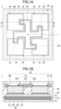
- FIGS. 1A and 1B are drawings illustrating a semiconductor apparatus according to a first embodiment, FIG. 1A is a plan view, and FIG. 1B is a cross-sectional view taken along the line A-A in FIG. 1A .
- a semiconductor apparatus 1 includes an interconnect substrate 10, a plurality of semiconductor devices 20, an interconnect substrate 30, a joint 40, and an encapsulating resin 50. It suffices for the present invention to have 3 or more semiconductor devices.
- the first embodiment is directed to an example in which 4 semiconductor devices 20 are provided.
- the interconnect substrate 30 side of the semiconductor apparatus 1 is defined as an upper side, and the interconnect substrate 10 side is defined as a lower side. Further, the surface of a portion on the upper side is defined as an upper surface, and the surface of a portion on the lower side is defined as a lower surface. It should be noted, however, that the semiconductor apparatus 1 may be placed upside down when used, or may be arranged at an any angle.
- the plan view refers to the view of an object as seen from the direction normal to the upper surface of the interconnect substrate 30, and the plane shape refers to the shape of an object as viewed from the direction normal to the upper surface of the interconnect substrate 30.
- the interconnect substrate 10 is formed in a flat plate shape.
- the interconnect substrate 10 may have any plane shape and any size. In the example illustrated in FIGS. 1A and 1B , the plane shape of the interconnect substrate 10 is rectangular.
- the interconnect substrate 10 includes an insulating layer 11, a metal layer 12, and a metal layer 13.
- the coefficient of thermal expansion of the interconnect substrate 10 may be, for example, about 2 ppm/°C to 7 ppm/°C.
- the insulating layer 11 may be formed of, for example, ceramics such as oxide-based ceramics or non-oxide-based ceramics.
- ceramics such as oxide-based ceramics or non-oxide-based ceramics.
- oxide-based ceramics include aluminum oxide (Al 2 O 3 ) and zirconia (ZrO 2 ).
- non-oxide-based ceramics include aluminum nitride (AlN) and silicon nitride (Si 3 N 4 ).
- the thickness of the insulating layer 11 may be, for example, about 200 um to 400 um.
- the metal layer 12 is formed on the upper surface of the insulating layer 11.
- the metal layer 12 may have any pattern.
- the metal layer 12 may be formed as a solid, continuous structure.
- the metal layer 13 may be used for electrical connection as an interconnect layer.
- the thickness of the metal layer 12 may be, for example, about 100 um to 800 um.
- the coefficient of thermal expansion of the metal layer 12 may be, for example, about 15 ppm/°C to 18ppm/°C.
- a surface treatment layer may be formed on the surface (both the upper surface and the sides surfaces, or only the upper surface) of the metal layer 12.
- the surface treatment layer include a metal layer such as an Au layer, an Ni layer/Au layer, an Ni layer/Pd layer/Au layer, and an Ni layer/Ag layer.
- a metal layer formed by an electroless plating method i.e., electroless plating metal layer
- the Au layer is a metal layer made of Au or Au alloy.
- the Ni layer is a metal layer made of Ni or Ni alloy.
- the Pd layer is a metal layer made of Pd or Pd alloy.
- the Ag layer is a metal layer made of Ag or Ag alloy.
- the metal layer 13 is formed on the lower surface of the insulating layer 11.
- the metal layer 13 may have any pattern.
- the metal layer 13 may be formed as a solid, continuous structure.
- the metal layer 13 may extend, for example, over the entire lower surface of the insulating layer 11 except for the outer perimeter edge.
- the metal layer 13 may not be used for electrical connection.
- the metal layer 13 may be used, for example, as a reinforcing layer for suppressing warpage or the like of the interconnect substrate 10.
- the metal layer 13 may also be used as a heat dissipating member.
- the material of the metal layer 13 for example, copper or a copper alloy may be used. If necessary, the same surface treatment layer as previously described may be formed on the surface (both the lower surface and the side surfaces, or only the lower surface) of the metal layer 13.
- the thickness of the metal layer 13 may be, for example, about 100 um to 800 um.
- the thickness of the metal layer 13 may be, for example, the same as that of the metal layer 12 or thinner than that of the metal layer 12.
- Each semiconductor device 20 is bonded to the upper surface of the metal layer 12 of the interconnect substrate 10 via the joint 40 which is electrically conductive.
- a sintered metal material may be used as the material of the joint 40.
- the sintered material for example, a sintered material mainly composed of silver (Ag) particles (i.e., silver sintering material) or a sintered material mainly composed of copper particles (i.e., copper sintering material) may be used.
- the material of the joint 40 may be, for example, a conductive paste such as solder or silver paste, or a metal brazing filler metal.
- the thickness of the joint 40 may be, for example, about 20 um to 60 um.
- Each semiconductor device 20 is, for example, a power semiconductor device.
- Each semiconductor device 20 has a control electrode and is switched by a voltage applied to the control electrode.
- Examples of the semiconductor device 20 include an insulated gate bipolar transistor (IGBT), a metal-oxide-semiconductor field-effect transistor (MOSFET), a diode, and the like.
- the semiconductor device 20 is a MOSFET.
- the plane shape of the semiconductor device 20 may be any shape with any size.
- the plane shape of the semiconductor device 20 is, for example, rectangular.
- the thickness of the semiconductor device 20 may be, for example, about 50 um to 600 um.
- the coefficient of thermal expansion of the semiconductor device 20 may be, for example, about 3 ppm/°C to 6 ppm/°C.
- the semiconductor device 20 includes a semiconductor substrate 21, an electrode 22, an electrode 23, and an electrode 24.
- the electrode 23 is a control electrode of the semiconductor device 20.
- the semiconductor substrate 21 is formed of, for example, silicon (Si) or silicon carbide (SiC).
- the electrodes 22 and 23 are formed on the upper surface of each semiconductor substrate 21.
- the electrodes 22 and 23 are situated apart from each other.
- the electrode 22 is, for example, substantially rectangular in plan view, and has a recess 22x setting back on one side.
- the electrode 23 may be located in the recesses 22x and spaced from the electrode 22 in plan view.
- the electrode 22 is, for example, the source electrode of the MOSFET.
- the electrode 23 is, for example, the gate electrode of the MOSFET.
- the electrode 24 is formed on the lower surface of each semiconductor substrate 21.
- the electrode 24 is, for example, the drain electrode of the MOSFET.
- a metal such as aluminum (Al) or copper (Cu), or an alloy containing at least one metal selected from these metals may be used. If necessary, the same surface treatment layer as previously described may be formed on the surfaces of the electrodes 22, 23, and 24.
- Each semiconductor device 20 is arranged at a constant rotation angle relative to the adjacent semiconductor device 20.
- each semiconductor device 20 is arranged at a rotation angle of 90 degrees relative to the adjacent semiconductor device 20. That is, in FIG. 1A , the upper-right semiconductor device 20 is arranged at a clockwise rotation angle of 90 degrees relative to the upper-left semiconductor device 20.
- the lower-right semiconductor device 20 is arranged at a clockwise rotation angle of 90 degrees relative to the upper-right semiconductor device 20.
- the lower-left semiconductor device 20 is arranged at a clockwise rotation angle of 90 degrees relative to the lower-right semiconductor device 20.
- the upper-left semiconductor device 20 is arranged at a clockwise rotation angle of 90 degrees relative to the lower-left semiconductor device 20. Whether or not the semiconductor devices 20 are rotated may be confirmed by the positions of the electrodes 23 in plan view.
- the interconnect substrate 30 is disposed on the semiconductor devices 20.
- the interconnect substrate 30 is formed in a flat plate shape.
- the interconnect substrate 30 may have any plane shape and any size. In the example illustrated in FIGS. 1A and 1B , the plane shape of the interconnect substrate 30 is rectangular.
- the thickness of the interconnect substrate 30 may be, for example, about 200 um to 400 um.
- the thermal expansion coefficient of the interconnect substrate 30 may be, for example, about 20 ppm/°C to 25 ppm/°C.
- the interconnect substrate 30 may be provided such as to exactly overlap the interconnect substrate 10 in plan view.
- the interconnect substrate 30 includes an insulating layer 31, an adhesive layer 32, and an interconnect layer 33.
- the insulating layer 31 is adhered to the semiconductor device 20 by the adhesive layer 32.
- an insulating resin such as a polyimide-based resin or a polyester-based resin may be used.
- the thickness of the insulating layer 31 may be, for example, about 30 um to 100 um.
- the adhesive layer 32 is formed on the lower surface of the insulating layer 31.
- the thickness of the adhesive layer 32 may be, for example, about 20 um to 45 um.
- the adhesive layer 32 may be, for example, an epoxy-based, polyimide-based, or silicone-based adhesive.
- the adhesive layer 32 may be provided so as to encompass, for example, a part of the semiconductor device 20. In other words, a part of the semiconductor device 20 may be embedded in the adhesive layer 32. For example, the outer perimeter edges of the electrodes 22 and 23 of the semiconductor device 20 may be embedded in the adhesive layer 32. An upper part of the side surface of the semiconductor device 20 may be covered with the adhesive layer 32.
- the interconnect substrate 30 has through-holes 30x formed through the insulating layer 31 and the adhesive layer 32 in the thickness direction.
- the through-holes 30x are each formed to expose a part of the upper surfaces of the electrodes 22 and 23, for example.
- the plane shape of each of the through-holes 30x is, for example, circular.
- One through-hole 30x may be provided at a position corresponding to each electrode.
- the interconnect layer 33 is formed on one side of the insulating layer 31.
- the interconnect layer 33 may include interconnect patterns 331 and 332 arranged on the one side of the insulating layer 31.
- the interconnect patterns 331 and 332 are arranged on the opposite side from the semiconductor device 20 across the insulating layer 31.
- the interconnect patterns 331 and 332 each include a planar interconnect formed on the upper surface of the insulating layer 31 and via interconnects formed in the through-holes 30x. In the example of FIG. 1A , the interconnect pattern 331 is surrounded by the interconnect pattern 332 in plan view.
- the interconnect pattern 331 connects the electrodes 23, which are the control electrodes of the semiconductor devices 20.
- the interconnect pattern 332 connects the electrodes 22 of the semiconductor devices 20.
- the metal layer 12 of the interconnect substrate 10 connects the electrodes 24 of the semiconductor devices 20. With this arrangement, the semiconductor devices 20 are connected in parallel with each other.
- the interconnect pattern 331 includes the same number of interconnects of equal length as the semiconductor devices 20, and also includes a voltage input point I for inputting a voltage to the electrodes 23, which are the control electrodes of the semiconductor devices 20, via the interconnects of equal length.
- the interconnects of equal length connect the voltage input point I with the electrodes 23.
- the voltage input point I is defined at the position equidistant from the electrodes 23.
- four L-shaped interconnects of equal length are connected to each other in the proximity of the voltage input point I in plan view, such that the interconnect pattern 331 has a swastika shape.
- the interconnects of equal length preferably has the same width.
- the material of the interconnect layer 33 for example, copper or a copper alloy may be used. If necessary, the same surface treatment layer as previously described may be formed on the surface (both the upper surface and the side surfaces, or only the upper surface) of the interconnect layer 33.
- the thermal expansion coefficient of the interconnect layer 33 may be, for example, about 15 ppm/°C to 18 ppm/°C.
- the thickness of the interconnect layer 33 may be, for example, about 50 um to 200 um.
- the interconnect pattern 331 and the electrodes 23 serving as the control electrodes of the semiconductor devices 20 may have n-fold symmetry with respect to the voltage input point I in plan view.
- the interconnect pattern 331 and the electrodes 23 serving as the control electrodes of the semiconductor devices 20 have 4-fold symmetry with respect to the voltage input point I in plan view.
- the encapsulating resin 50 encapsulates the semiconductor device 20 provided between the interconnect substrate 10 and the interconnect substrate 30.
- a non-photosensitive insulating resin mainly composed of a thermosetting resin may be used as the material of the encapsulating resin 50.
- the material of the encapsulating resin 50 may be, for example, an insulating resin such as an epoxy-based resin or a polyimide-based resin, or a resin material in which a filler such as silica or alumina is mixed with such a resin.
- a mold resin may be used as the encapsulating resin 50.
- the thermal expansion coefficient of the encapsulating resin 50 may be, for example, about 5ppm/°C to 18 ppm/°C.
- the metal layer 12 extends to the outside of the encapsulating resin 50 in order to enable electrical connection.
- the semiconductor apparatus 1 is such that the electrodes 23 (e.g., the gate electrode of a MOSFET), which are the control electrodes of the semiconductor devices 20, are connected to the voltage input point I only through the equal length interconnects extending in different directions from the voltage input point I. That is, the interconnects connected from the voltage input point I to the electrodes 23, which are the control electrodes of the semiconductor devices 20, have the same length.
- This arrangement enables the reduction of timing deviation when the control voltage is input from the voltage input point I to the semiconductor devices 20 to cause the semiconductor devices 20 to be simultaneously switched.
- the equal-length interconnects connected from the voltage input point I to the electrodes 23 serving as the control electrodes of the respective semiconductor devices 20 may be made to have the same width, which further enhances the above-described advantageous effects.
- the semiconductor devices 20 are preferably arranged at a constant rotation angle relative to the adjacent semiconductor devices 20, which allows the respective electrodes 23 to be easily connected to the voltage input point I through equal-length interconnects.
- the semiconductor devices 20 are arranged at a rotation angle of 90 degrees relative to the adjacent semiconductor devices 20, the crystal orientations of the semiconductor devices 20 differ from each other, thereby serving to improve the apparent strength of the semiconductor apparatus 1.
- the control electrodes of semiconductor devices are not connected to a voltage input point only through equal-length interconnects extending in different directions from the voltage input point.
- the gate circuit pattern is configured by connecting an L-shaped portion 24a in plan view and an H-shaped portion 24b in plan view. This configuration is not preferable in that current concentration easily occurs in a semiconductor device. For example, at the time of turning off the semiconductor devices, current is temporarily concentrated in a semiconductor device with a low threshold voltage due to variations in the gate threshold voltage.
- the H-shaped portion 24b branches into two sections on the left and branches into two sections on the right. If there is a deviation that increases the threshold voltage in one of the two sections on either side, the current is likely to be concentrated in the other section. In such a case, the likelihood of oscillation increases.
- the semiconductor apparatus 1 is such that the electrodes 23, which are the control electrodes of the semiconductor devices 20, are connected to the voltage input point I only through the respective equal-length interconnects extending in different directions from the voltage input point I, and the interconnect pattern 331 does not have branches as in Patent Document 1.
- the other three semiconductor devices 20 are equally capable of receiving current. As a result, current concentration in a particular semiconductor device 20 is unlikely to occur, and oscillation is also unlikely to occur.
- the semiconductor apparatus 1 may not have the interconnect substrate 10.
- the metal layer 12 for connecting the electrodes 24 to each other is provided on the lower surface side of the semiconductor devices 20.
- the semiconductor apparatus 1 may have only the metal layer 12 instead of the interconnect substrate 10.
- an insulating layer 31 in a sheet form is prepared, and an adhesive layer 32 is formed on the lower surface of the insulating layer 31.
- Through-holes 30x are then formed in required portions of the insulating layer 31 and the adhesive layer 32.
- the through-holes 30x may be formed by a laser processing method using, for example, a CO 2 laser or a UV-YAG laser.
- semiconductor devices 20 are fixed to the lower surface of the insulating layer 31 through the adhesive layer 32.
- the upper surfaces of the electrodes 22 and 23 are partially exposed in the through-holes 30x.
- an interconnect layer 33 is formed on the insulating layer 31.
- the interconnect layer 33 includes the interconnect patterns 331 and 332 arranged on the same side of the insulating layer 31.
- the interconnect pattern 331 is electrically connected to the electrodes 23, and the interconnect pattern 332 is electrically connected to the electrodes 22.
- the interconnect patterns 331 and 332 are formed in the pattern illustrated in FIG. 1A .
- the interconnect patterns 331 and 332 each include a planar interconnect formed on the upper surface of the insulating layer 31 and via interconnects formed in the through-holes 30x.
- the interconnect patterns 331 and 332 may be formed by various interconnect forming methods such as a semi-additive method.
- an interconnect substrate 10 having a metal layer 12 formed on the upper surface and a metal layer 13 formed on the lower surface is prepared.
- joints 40 are formed on the upper surface of the metal layer 12.
- the joints 40 are formed at four locations where the semiconductor devices 20 illustrated in FIG. 1 are arranged.
- the joints 40 may be formed by applying, for example, a sintered material in paste form (i.e., sintering paste) by a printing method or a dispenser method.
- sintering paste for example, silver sintering paste in which silver particles are dispersed in an organic solvent may be used.
- the printing method for example, a screen printing method or a stencil printing method may be used.
- the semiconductor devices 20 mounted on the interconnect substrate 30 are placed on the upper surfaces of the respective joints 40.
- the semiconductor devices 20 are placed on the upper surfaces of the joints 40 such that the electrodes 24 formed on the lower surfaces of the semiconductor devices 20 are in contact with the upper surfaces of the joints 40.
- the joints 40 are then sintered by heating the joints 40.
- the metal layer 12 and the electrodes 24 of the semiconductor devices 20 are joined by the joints 40. That is, the semiconductor devices 20 are joined on the metal layer 12 via the joints 40.
- the electrodes 24 of the semiconductor devices 20 are connected in parallel via the metal layer 12.
- an encapsulating resin 50 for encapsulating the semiconductor devices 20 provided between the interconnect substrate 10 and the interconnect substrate 30 is formed.
- the encapsulating resin 50 may be formed, for example, in such a manner as to expose the upper surface of the interconnect layer 33 and the lower surface of the metal layer 13 and cover the other surfaces.
- the encapsulating resin 50 may be formed, for example, by using a method such as a transfer molding method, a compression molding method, or an injection molding method.
- Variations of the first embodiment are directed to examples of a semiconductor apparatus different from the first embodiment in the number of semiconductor devices, the shape of interconnect patterns, or the like. With respect to these variations of the first embodiment, descriptions of the same components as those of the already described embodiment may be omitted as appropriate.
- FIGS. 4A and 4B are drawings illustrating a semiconductor apparatus according to a first variation of the first embodiment.
- FIG. 4A is a plan view
- FIG. 4B is a cross-sectional view taken along the line B-B in FIG. 4A .
- a semiconductor apparatus 1A differs from the semiconductor apparatus 1 in that degas holes 30y are formed through the interconnect substrate 30.
- the degas holes 30y are holes for degassing. Through-holes 332x are provided at those portions of the interconnect pattern 332 which overlap the degas holes 30y in plan view. That is, the degas holes 30y are provided at positions where the degas holes do not overlap with the interconnect patterns 331 and 332 in plan view.
- the degas holes 30y are filled with the encapsulating resin 50. In the example illustrated in FIGS. 4A and 4B , four degas holes 30y are provided, but the number of degas holes y may be any number that is greater than or equal to one.
- gas generated in the semiconductor apparatus 1A during heating may be released to the outside in the step of forming the encapsulating resin 50 of the semiconductor apparatus 1A. This may reduce the risk of voids occurring in the encapsulating resin 50.
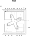
- FIG. 5 is a plan view illustrating a semiconductor apparatus according to a second variation of the first embodiment.
- a semiconductor apparatus 1B differs from the semiconductor apparatus 1 in the shape of the interconnect pattern 331.
- the interconnect pattern 331 has a cross shape.
- the voltage input point I is located at the center of the cross.
- all imaginary straight lines connecting the center of each of the electrodes 23 of the semiconductor devices 20 to the voltage input point I overlap with the interconnect pattern 331.
- the distance between the voltage input point I and each electrode 23 may be made to be the shortest. This arrangement further reduces the timing deviation when the control voltage is input from the voltage input point I to each semiconductor device 20 to cause the simultaneous switching operation of each semiconductor device 20.
- FIG. 6 is a plan view illustrating a semiconductor apparatus according to a third variation of the first embodiment.
- a semiconductor apparatus 1C differs from the semiconductor apparatus 1 having the four semiconductor devices 20 in that three semiconductor devices 20 are provided.
- the semiconductor apparatus may include three semiconductor devices 20.
- the semiconductor apparatus 1C three equal-length linear interconnects are connected together in the proximity of the voltage input point I in plan view, and the interconnect pattern 331 is T-shaped.
- the semiconductor apparatus 1C provides the same advantageous effects as the semiconductor apparatus 1B.
- FIGS. 7A and 7B are drawings illustrating a semiconductor apparatus according to a fourth variation of the first embodiment, FIG. 7A is a plan view, and FIG. 7B is a cross-sectional view taken along the line C-C in FIG. 7A .
- a semiconductor apparatus 1D differs from the semiconductor apparatus 1 in that a connecting member 60 is provided.
- the lower surface of the connecting member 60 is electrically connected to the metal layer 12 of the interconnect substrate 10 via the joint 40. It may be noted that, the connecting member 60 is connected to an interconnect pattern of the metal layer 12 different from the interconnect patterns connected to the electrodes 24 of the semiconductor devices 20.
- the upper surface of the connecting member 60 is electrically connected to the interconnect pattern 331 of the interconnect substrate 30. Thus, the interconnect pattern 331 is electrically connected to the metal layer 12 via the connecting member 60.
- the connecting member 60 is, for example, a columnar shape extending in the thickness direction of the semiconductor apparatus 1D.
- the connecting member 60 is, for example, a metal post.
- As the material of the connecting member 60 for example, copper or a copper alloy may be used.
- the connecting member 60 may be, for example, substantially the same thickness as the semiconductor device 20.
- the thickness of the connecting member 60 may be, for example, approximately 50 um to 600 um.
- the upper surface of the connecting member 60 may be, for example, flush with the upper surfaces of the electrodes 22 and 23 of the semiconductor devices 20.
- the interconnect pattern 331 of the interconnect substrate 30 may include an interconnect electrically connected to the metal layer 12 via the connecting member 60. That is, the connecting member 60 may be arranged in a region where the semiconductor device 20 is not arranged in plan view so as to connect the interconnect pattern 331 of the interconnect substrate 30 and the metal layer 12 of the interconnect substrate 10.
- the length of the interconnect may not be equal to the length of the three equal length interconnects.
- a voltage is input into the voltage input point I via the metal layer 12 and the connecting member 60.
- FIG. 8 is a plan view illustrating a semiconductor apparatus according to a fifth variation of the first embodiment.
- a semiconductor apparatus 1E differs from the semiconductor apparatus 1 having the four semiconductor devices 20 in that six semiconductor devices 20 are provided.
- the semiconductor apparatus may have six semiconductor devices 20.
- the semiconductor apparatus 1E in plan view, six linear equal length interconnects are connected together in the proximity of the voltage input point I.
- the interconnect pattern 331 and the electrodes 23, which are the control electrodes of the semiconductor devices 20 have 6-fold symmetry with respect to the voltage input point I and also have 12-fold symmetry.
- the semiconductor apparatus 1E provides the same advantageous effects as the semiconductor apparatus 1B.
- a semiconductor apparatus may reduce timing deviation when a plurality of semiconductor devices need to be simultaneously switched.
Landscapes
- Internal Circuitry In Semiconductor Integrated Circuit Devices (AREA)
- Physics & Mathematics (AREA)
- Geometry (AREA)
Abstract
Description
- The disclosures herein generally relate to semiconductor apparatuses.
- A power-system semiconductor apparatus (i.e., power module) as known in the art controls or supplies electric power. This type of semiconductor apparatus includes, for example, a plurality of semiconductor devices having respective gate electrodes, and the gate electrodes are electrically connected to each other to switch the plurality of semiconductor devices simultaneously (for example, see Patent Document 1).
- When a plurality of semiconductor devices need to be simultaneously switched, aligning the timing of the switching operations presents a challenge.
- Accordingly, there may be a need for a semiconductor apparatus which may reduce timing deviation when a plurality of semiconductor devices need to be simultaneously switched.
- [Patent Document 1]
Japanese Unexamined Patent Publication No. 2021-125546 - According to an aspect of the embodiment, a semiconductor apparatus includes three or more semiconductor devices connected in parallel with each other and an interconnect substrate arranged on the semiconductor devices, wherein the semiconductor devices have respective control electrodes and are switched by a voltage applied to the control electrodes, wherein the interconnect substrate includes an insulating layer and a first interconnect pattern arranged on an opposite side of the insulating layer from the semiconductor devices and connecting the control electrodes of the semiconductor devices, wherein the first interconnect pattern includes a same number of interconnects of equal length as the semiconductor devices, and a voltage input point configured to receive a voltage applied to the control electrodes of the semiconductor devices via the interconnects of equal length, and wherein the control electrodes of the semiconductor devices are connected to the voltage input point only by the interconnects of equal length, which extend in different directions from the voltage input point.
-
-
FIGS. 1A and 1B are drawings illustrating a semiconductor apparatus according to a first embodiment; -
FIGS. 2A through 2C are drawings illustrating a manufacturing process of a semiconductor apparatus according to the first embodiment; -
FIGS. 3A and 3B are drawings illustrating the manufacturing process of a semiconductor apparatus according to the first embodiment; -
FIGS. 4A and 4B are drawings illustrating a semiconductor apparatus according to a first variation of the first embodiment; -
FIG. 5 is a plan view illustrating a semiconductor apparatus according to a second variation of the first embodiment; -
FIG. 6 is a plan view illustrating a semiconductor apparatus according to a third variation of the first embodiment; -
FIGS. 7A and 7B are drawings illustrating a semiconductor apparatus according to a fourth variation of the first embodiment; and -
FIG. 8 is a plan view illustrating a semiconductor apparatus according to a fifth variation of the first embodiment. - In the following, embodiments for carrying out the invention will be described with reference to the accompanying drawings. In these drawings, the same components are referred to by the same reference numerals, and a duplicate description thereof may be omitted.
-
FIGS. 1A and 1B are drawings illustrating a semiconductor apparatus according to a first embodiment,FIG. 1A is a plan view, andFIG. 1B is a cross-sectional view taken along the line A-A inFIG. 1A . - Referring to
FIGS. 1A and 1B , asemiconductor apparatus 1 includes aninterconnect substrate 10, a plurality ofsemiconductor devices 20, aninterconnect substrate 30, ajoint 40, and anencapsulating resin 50. It suffices for the present invention to have 3 or more semiconductor devices. The first embodiment is directed to an example in which 4semiconductor devices 20 are provided. - In the present embodiment, for the sake of convenience, the
interconnect substrate 30 side of thesemiconductor apparatus 1 is defined as an upper side, and theinterconnect substrate 10 side is defined as a lower side. Further, the surface of a portion on the upper side is defined as an upper surface, and the surface of a portion on the lower side is defined as a lower surface. It should be noted, however, that thesemiconductor apparatus 1 may be placed upside down when used, or may be arranged at an any angle. The plan view refers to the view of an object as seen from the direction normal to the upper surface of theinterconnect substrate 30, and the plane shape refers to the shape of an object as viewed from the direction normal to the upper surface of theinterconnect substrate 30. - The
interconnect substrate 10 is formed in a flat plate shape. Theinterconnect substrate 10 may have any plane shape and any size. In the example illustrated inFIGS. 1A and 1B , the plane shape of theinterconnect substrate 10 is rectangular. - The
interconnect substrate 10 includes aninsulating layer 11, ametal layer 12, and ametal layer 13. The coefficient of thermal expansion of theinterconnect substrate 10 may be, for example, about 2 ppm/°C to 7 ppm/°C. - The
insulating layer 11 may be formed of, for example, ceramics such as oxide-based ceramics or non-oxide-based ceramics. Examples of the oxide-based ceramics include aluminum oxide (Al2O3) and zirconia (ZrO2). Examples of the non-oxide-based ceramics include aluminum nitride (AlN) and silicon nitride (Si3N4). The thickness of theinsulating layer 11 may be, for example, about 200 um to 400 um. - The
metal layer 12 is formed on the upper surface of theinsulating layer 11. Themetal layer 12 may have any pattern. Themetal layer 12 may be formed as a solid, continuous structure. Themetal layer 13 may be used for electrical connection as an interconnect layer. As the material of themetal layer 12, for example, copper or a copper alloy may be used. The thickness of themetal layer 12 may be, for example, about 100 um to 800 um. The coefficient of thermal expansion of themetal layer 12 may be, for example, about 15 ppm/°C to 18ppm/°C. - If necessary, a surface treatment layer may be formed on the surface (both the upper surface and the sides surfaces, or only the upper surface) of the
metal layer 12. Examples of the surface treatment layer include a metal layer such as an Au layer, an Ni layer/Au layer, an Ni layer/Pd layer/Au layer, and an Ni layer/Ag layer. As the Au layer, Ni layer, Pd layer, and Ag layer, for example, a metal layer formed by an electroless plating method (i.e., electroless plating metal layer) may be used. The Au layer is a metal layer made of Au or Au alloy. The Ni layer is a metal layer made of Ni or Ni alloy. The Pd layer is a metal layer made of Pd or Pd alloy. The Ag layer is a metal layer made of Ag or Ag alloy. - The
metal layer 13 is formed on the lower surface of the insulatinglayer 11. Themetal layer 13 may have any pattern. Themetal layer 13 may be formed as a solid, continuous structure. Themetal layer 13 may extend, for example, over the entire lower surface of the insulatinglayer 11 except for the outer perimeter edge. Themetal layer 13 may not be used for electrical connection. Themetal layer 13 may be used, for example, as a reinforcing layer for suppressing warpage or the like of theinterconnect substrate 10. Themetal layer 13 may also be used as a heat dissipating member. - As the material of the
metal layer 13, for example, copper or a copper alloy may be used. If necessary, the same surface treatment layer as previously described may be formed on the surface (both the lower surface and the side surfaces, or only the lower surface) of themetal layer 13. The thickness of themetal layer 13 may be, for example, about 100 um to 800 um. The thickness of themetal layer 13 may be, for example, the same as that of themetal layer 12 or thinner than that of themetal layer 12. - Each
semiconductor device 20 is bonded to the upper surface of themetal layer 12 of theinterconnect substrate 10 via the joint 40 which is electrically conductive. As the material of the joint 40, for example, a sintered metal material may be used. As the sintered material, for example, a sintered material mainly composed of silver (Ag) particles (i.e., silver sintering material) or a sintered material mainly composed of copper particles (i.e., copper sintering material) may be used. Alternatively, the material of the joint 40 may be, for example, a conductive paste such as solder or silver paste, or a metal brazing filler metal. The thickness of the joint 40 may be, for example, about 20 um to 60 um. - Each
semiconductor device 20 is, for example, a power semiconductor device. Eachsemiconductor device 20 has a control electrode and is switched by a voltage applied to the control electrode. Examples of thesemiconductor device 20 include an insulated gate bipolar transistor (IGBT), a metal-oxide-semiconductor field-effect transistor (MOSFET), a diode, and the like. - In the first embodiment, the
semiconductor device 20 is a MOSFET. The plane shape of thesemiconductor device 20 may be any shape with any size. The plane shape of thesemiconductor device 20 is, for example, rectangular. The thickness of thesemiconductor device 20 may be, for example, about 50 um to 600 um. The coefficient of thermal expansion of thesemiconductor device 20 may be, for example, about 3 ppm/°C to 6 ppm/°C. - The
semiconductor device 20 includes asemiconductor substrate 21, anelectrode 22, anelectrode 23, and anelectrode 24. Theelectrode 23 is a control electrode of thesemiconductor device 20. Thesemiconductor substrate 21 is formed of, for example, silicon (Si) or silicon carbide (SiC). - The
electrodes semiconductor substrate 21. Theelectrodes electrode 22 is, for example, substantially rectangular in plan view, and has arecess 22x setting back on one side. Theelectrode 23 may be located in therecesses 22x and spaced from theelectrode 22 in plan view. Theelectrode 22 is, for example, the source electrode of the MOSFET. Theelectrode 23 is, for example, the gate electrode of the MOSFET. Theelectrode 24 is formed on the lower surface of eachsemiconductor substrate 21. Theelectrode 24 is, for example, the drain electrode of the MOSFET. - As the materials of the
electrodes electrodes - Each
semiconductor device 20 is arranged at a constant rotation angle relative to theadjacent semiconductor device 20. In the first embodiment, eachsemiconductor device 20 is arranged at a rotation angle of 90 degrees relative to theadjacent semiconductor device 20. That is, inFIG. 1A , the upper-right semiconductor device 20 is arranged at a clockwise rotation angle of 90 degrees relative to the upper-leftsemiconductor device 20. The lower-right semiconductor device 20 is arranged at a clockwise rotation angle of 90 degrees relative to the upper-right semiconductor device 20. The lower-leftsemiconductor device 20 is arranged at a clockwise rotation angle of 90 degrees relative to the lower-right semiconductor device 20. The upper-leftsemiconductor device 20 is arranged at a clockwise rotation angle of 90 degrees relative to the lower-leftsemiconductor device 20. Whether or not thesemiconductor devices 20 are rotated may be confirmed by the positions of theelectrodes 23 in plan view. - The
interconnect substrate 30 is disposed on thesemiconductor devices 20. Theinterconnect substrate 30 is formed in a flat plate shape. Theinterconnect substrate 30 may have any plane shape and any size. In the example illustrated inFIGS. 1A and 1B , the plane shape of theinterconnect substrate 30 is rectangular. The thickness of theinterconnect substrate 30 may be, for example, about 200 um to 400 um. The thermal expansion coefficient of theinterconnect substrate 30 may be, for example, about 20 ppm/°C to 25 ppm/°C. For example, theinterconnect substrate 30 may be provided such as to exactly overlap theinterconnect substrate 10 in plan view. - The
interconnect substrate 30 includes an insulatinglayer 31, anadhesive layer 32, and aninterconnect layer 33. The insulatinglayer 31 is adhered to thesemiconductor device 20 by theadhesive layer 32. As the material of the insulatinglayer 31, for example, an insulating resin such as a polyimide-based resin or a polyester-based resin may be used. The thickness of the insulatinglayer 31 may be, for example, about 30 um to 100 um. - The
adhesive layer 32 is formed on the lower surface of the insulatinglayer 31. The thickness of theadhesive layer 32 may be, for example, about 20 um to 45 um. Theadhesive layer 32 may be, for example, an epoxy-based, polyimide-based, or silicone-based adhesive. Theadhesive layer 32 may be provided so as to encompass, for example, a part of thesemiconductor device 20. In other words, a part of thesemiconductor device 20 may be embedded in theadhesive layer 32. For example, the outer perimeter edges of theelectrodes semiconductor device 20 may be embedded in theadhesive layer 32. An upper part of the side surface of thesemiconductor device 20 may be covered with theadhesive layer 32. - The
interconnect substrate 30 has through-holes 30x formed through the insulatinglayer 31 and theadhesive layer 32 in the thickness direction. The through-holes 30x are each formed to expose a part of the upper surfaces of theelectrodes holes 30x is, for example, circular. One through-hole 30x may be provided at a position corresponding to each electrode. - The
interconnect layer 33 is formed on one side of the insulatinglayer 31. Theinterconnect layer 33 may includeinterconnect patterns layer 31. Theinterconnect patterns semiconductor device 20 across the insulatinglayer 31. Theinterconnect patterns layer 31 and via interconnects formed in the through-holes 30x. In the example ofFIG. 1A , theinterconnect pattern 331 is surrounded by theinterconnect pattern 332 in plan view. - The
interconnect pattern 331 connects theelectrodes 23, which are the control electrodes of thesemiconductor devices 20. Theinterconnect pattern 332 connects theelectrodes 22 of thesemiconductor devices 20. Themetal layer 12 of theinterconnect substrate 10 connects theelectrodes 24 of thesemiconductor devices 20. With this arrangement, thesemiconductor devices 20 are connected in parallel with each other. - The
interconnect pattern 331 includes the same number of interconnects of equal length as thesemiconductor devices 20, and also includes a voltage input point I for inputting a voltage to theelectrodes 23, which are the control electrodes of thesemiconductor devices 20, via the interconnects of equal length. InFIG. 1A , the interconnects of equal length connect the voltage input point I with theelectrodes 23. In other words, the voltage input point I is defined at the position equidistant from theelectrodes 23. In the example illustrated inFIG. 1A , four L-shaped interconnects of equal length are connected to each other in the proximity of the voltage input point I in plan view, such that theinterconnect pattern 331 has a swastika shape. The interconnects of equal length preferably has the same width. - As the material of the
interconnect layer 33, for example, copper or a copper alloy may be used. If necessary, the same surface treatment layer as previously described may be formed on the surface (both the upper surface and the side surfaces, or only the upper surface) of theinterconnect layer 33. The thermal expansion coefficient of theinterconnect layer 33 may be, for example, about 15 ppm/°C to 18 ppm/°C. The thickness of theinterconnect layer 33 may be, for example, about 50 um to 200 um. - In the present invention, when there are n semiconductor devices (n is a natural number equal to or greater than 3), the
interconnect pattern 331 and theelectrodes 23 serving as the control electrodes of thesemiconductor devices 20 may have n-fold symmetry with respect to the voltage input point I in plan view. In the example illustrated inFIGS. 1A and 1B , there are foursemiconductor devices 20, and theinterconnect pattern 331 and theelectrodes 23 serving as the control electrodes of thesemiconductor devices 20 have 4-fold symmetry with respect to the voltage input point I in plan view. - The encapsulating
resin 50 encapsulates thesemiconductor device 20 provided between theinterconnect substrate 10 and theinterconnect substrate 30. As the material of the encapsulatingresin 50, for example, a non-photosensitive insulating resin mainly composed of a thermosetting resin may be used. Specifically, the material of the encapsulatingresin 50 may be, for example, an insulating resin such as an epoxy-based resin or a polyimide-based resin, or a resin material in which a filler such as silica or alumina is mixed with such a resin. As the encapsulatingresin 50, for example, a mold resin may be used. The thermal expansion coefficient of the encapsulatingresin 50 may be, for example, about 5ppm/°C to 18 ppm/°C. Themetal layer 12 extends to the outside of the encapsulatingresin 50 in order to enable electrical connection. - As described above, the
semiconductor apparatus 1 is such that the electrodes 23 (e.g., the gate electrode of a MOSFET), which are the control electrodes of thesemiconductor devices 20, are connected to the voltage input point I only through the equal length interconnects extending in different directions from the voltage input point I. That is, the interconnects connected from the voltage input point I to theelectrodes 23, which are the control electrodes of thesemiconductor devices 20, have the same length. This arrangement enables the reduction of timing deviation when the control voltage is input from the voltage input point I to thesemiconductor devices 20 to cause thesemiconductor devices 20 to be simultaneously switched. Furthermore, it is possible to equalize the currents flowing through the electrodes 24 (e.g., the drain electrode of a MOSFET) of thesemiconductor devices 20. It may be noted that the equal-length interconnects connected from the voltage input point I to theelectrodes 23 serving as the control electrodes of therespective semiconductor devices 20 may be made to have the same width, which further enhances the above-described advantageous effects. - In addition, the
semiconductor devices 20 are preferably arranged at a constant rotation angle relative to theadjacent semiconductor devices 20, which allows therespective electrodes 23 to be easily connected to the voltage input point I through equal-length interconnects. When thesemiconductor devices 20 are arranged at a rotation angle of 90 degrees relative to theadjacent semiconductor devices 20, the crystal orientations of thesemiconductor devices 20 differ from each other, thereby serving to improve the apparent strength of thesemiconductor apparatus 1. - In the example illustrated in
FIG. 3 ofPatent Document 1, the control electrodes of semiconductor devices are not connected to a voltage input point only through equal-length interconnects extending in different directions from the voltage input point. In the example illustrated inFIG. 3 ofPatent Document 1, the gate circuit pattern is configured by connecting an L-shaped portion 24a in plan view and an H-shaped portion 24b in plan view. This configuration is not preferable in that current concentration easily occurs in a semiconductor device. For example, at the time of turning off the semiconductor devices, current is temporarily concentrated in a semiconductor device with a low threshold voltage due to variations in the gate threshold voltage. In the configuration disclosed inPatent Document 1, the H-shaped portion 24b branches into two sections on the left and branches into two sections on the right. If there is a deviation that increases the threshold voltage in one of the two sections on either side, the current is likely to be concentrated in the other section. In such a case, the likelihood of oscillation increases. - On the other hand, the
semiconductor apparatus 1 is such that theelectrodes 23, which are the control electrodes of thesemiconductor devices 20, are connected to the voltage input point I only through the respective equal-length interconnects extending in different directions from the voltage input point I, and theinterconnect pattern 331 does not have branches as inPatent Document 1. With this arrangement, even when there is a deviation that increases the threshold voltage in one of thesemiconductor devices 20, the other threesemiconductor devices 20 are equally capable of receiving current. As a result, current concentration in aparticular semiconductor device 20 is unlikely to occur, and oscillation is also unlikely to occur. - In addition, when branches exist as in the configuration of
Patent Document 1, the resin needs to go around both sides of the branches when forming the encapsulating resin, so that voids are likely to be formed in the encapsulating resin. In thesemiconductor apparatus 1, since theinterconnect pattern 331 does not have branches as inPatent Document 1, resin flows easily, and voids are unlikely to be formed in the encapsulating resin. - The
semiconductor apparatus 1 may not have theinterconnect substrate 10. In this case, themetal layer 12 for connecting theelectrodes 24 to each other is provided on the lower surface side of thesemiconductor devices 20. In other words, thesemiconductor apparatus 1 may have only themetal layer 12 instead of theinterconnect substrate 10. - In the following, a method of making the
semiconductor apparatus 1 will be described. For convenience of explanation, parts that eventually become the respective components of thesemiconductor apparatus 1 will be designated by the reference numerals of the final components. - First, in a step illustrated in
FIG. 2A , an insulatinglayer 31 in a sheet form is prepared, and anadhesive layer 32 is formed on the lower surface of the insulatinglayer 31. Through-holes 30x are then formed in required portions of the insulatinglayer 31 and theadhesive layer 32. The through-holes 30x may be formed by a laser processing method using, for example, a CO2 laser or a UV-YAG laser. - Next, in a step illustrated in
FIG. 2B ,semiconductor devices 20 are fixed to the lower surface of the insulatinglayer 31 through theadhesive layer 32. When thesemiconductor devices 20 are fixed, the upper surfaces of theelectrodes holes 30x. - In a step illustrated in
FIG. 2C , aninterconnect layer 33 is formed on the insulatinglayer 31. With this, the fabrication of theinterconnect substrate 30 having the insulatinglayer 31, theadhesive layer 32, and theinterconnect layer 33 is completed. Theinterconnect layer 33 includes theinterconnect patterns layer 31. Theinterconnect pattern 331 is electrically connected to theelectrodes 23, and theinterconnect pattern 332 is electrically connected to theelectrodes 22. Theinterconnect patterns FIG. 1A . Theinterconnect patterns layer 31 and via interconnects formed in the through-holes 30x. Theinterconnect patterns - In a step illustrated in
FIG. 3A , aninterconnect substrate 10 having ametal layer 12 formed on the upper surface and ametal layer 13 formed on the lower surface is prepared. Then, joints 40 are formed on the upper surface of themetal layer 12. Specifically, thejoints 40 are formed at four locations where thesemiconductor devices 20 illustrated inFIG. 1 are arranged. Thejoints 40 may be formed by applying, for example, a sintered material in paste form (i.e., sintering paste) by a printing method or a dispenser method. As the sintering paste, for example, silver sintering paste in which silver particles are dispersed in an organic solvent may be used. As the printing method, for example, a screen printing method or a stencil printing method may be used. - Subsequently, the
semiconductor devices 20 mounted on theinterconnect substrate 30 are placed on the upper surfaces of the respective joints 40. Specifically, thesemiconductor devices 20 are placed on the upper surfaces of thejoints 40 such that theelectrodes 24 formed on the lower surfaces of thesemiconductor devices 20 are in contact with the upper surfaces of thejoints 40. - The
joints 40 are then sintered by heating thejoints 40. As a result, themetal layer 12 and theelectrodes 24 of thesemiconductor devices 20 are joined by thejoints 40. That is, thesemiconductor devices 20 are joined on themetal layer 12 via thejoints 40. Theelectrodes 24 of thesemiconductor devices 20 are connected in parallel via themetal layer 12. - In a step illustrated in
FIG. 3B , an encapsulatingresin 50 for encapsulating thesemiconductor devices 20 provided between theinterconnect substrate 10 and theinterconnect substrate 30 is formed. The encapsulatingresin 50 may be formed, for example, in such a manner as to expose the upper surface of theinterconnect layer 33 and the lower surface of themetal layer 13 and cover the other surfaces. The encapsulatingresin 50 may be formed, for example, by using a method such as a transfer molding method, a compression molding method, or an injection molding method. Through the steps described above, the fabrication of thesemiconductor apparatus 1 is completed. - Variations of the first embodiment are directed to examples of a semiconductor apparatus different from the first embodiment in the number of semiconductor devices, the shape of interconnect patterns, or the like. With respect to these variations of the first embodiment, descriptions of the same components as those of the already described embodiment may be omitted as appropriate.
-
FIGS. 4A and 4B are drawings illustrating a semiconductor apparatus according to a first variation of the first embodiment.FIG. 4A is a plan view, andFIG. 4B is a cross-sectional view taken along the line B-B inFIG. 4A . Referring toFIGS. 4A and 4B , asemiconductor apparatus 1A differs from thesemiconductor apparatus 1 in thatdegas holes 30y are formed through theinterconnect substrate 30. - The degas holes 30y are holes for degassing. Through-
holes 332x are provided at those portions of theinterconnect pattern 332 which overlap thedegas holes 30y in plan view. That is, thedegas holes 30y are provided at positions where the degas holes do not overlap with theinterconnect patterns resin 50. In the example illustrated inFIGS. 4A and 4B , fourdegas holes 30y are provided, but the number of degas holes y may be any number that is greater than or equal to one. - By providing the degas holes 30y in the
interconnect substrate 30, gas generated in thesemiconductor apparatus 1A during heating may be released to the outside in the step of forming the encapsulatingresin 50 of thesemiconductor apparatus 1A. This may reduce the risk of voids occurring in the encapsulatingresin 50. -
FIG. 5 is a plan view illustrating a semiconductor apparatus according to a second variation of the first embodiment. Referring toFIG. 5 , asemiconductor apparatus 1B differs from thesemiconductor apparatus 1 in the shape of theinterconnect pattern 331. - In the
semiconductor apparatus 1B, in plan view, four linear equal-length interconnects are connected together in the proximity of the voltage input point I, and theinterconnect pattern 331 has a cross shape. The voltage input point I is located at the center of the cross. In plan view, all imaginary straight lines connecting the center of each of theelectrodes 23 of thesemiconductor devices 20 to the voltage input point I overlap with theinterconnect pattern 331. - By forming the
interconnect pattern 331 into a cross shape, the distance between the voltage input point I and eachelectrode 23 may be made to be the shortest. This arrangement further reduces the timing deviation when the control voltage is input from the voltage input point I to eachsemiconductor device 20 to cause the simultaneous switching operation of eachsemiconductor device 20. -
FIG. 6 is a plan view illustrating a semiconductor apparatus according to a third variation of the first embodiment. Referring toFIG. 6 , asemiconductor apparatus 1C differs from thesemiconductor apparatus 1 having the foursemiconductor devices 20 in that threesemiconductor devices 20 are provided. - As described above, the semiconductor apparatus may include three
semiconductor devices 20. In thesemiconductor apparatus 1C, three equal-length linear interconnects are connected together in the proximity of the voltage input point I in plan view, and theinterconnect pattern 331 is T-shaped. Thesemiconductor apparatus 1C provides the same advantageous effects as thesemiconductor apparatus 1B. -
FIGS. 7A and 7B are drawings illustrating a semiconductor apparatus according to a fourth variation of the first embodiment,FIG. 7A is a plan view, andFIG. 7B is a cross-sectional view taken along the line C-C inFIG. 7A . Referring toFIGS. 7A and 7B , asemiconductor apparatus 1D differs from thesemiconductor apparatus 1 in that a connectingmember 60 is provided. - The lower surface of the connecting
member 60 is electrically connected to themetal layer 12 of theinterconnect substrate 10 via the joint 40. It may be noted that, the connectingmember 60 is connected to an interconnect pattern of themetal layer 12 different from the interconnect patterns connected to theelectrodes 24 of thesemiconductor devices 20. The upper surface of the connectingmember 60 is electrically connected to theinterconnect pattern 331 of theinterconnect substrate 30. Thus, theinterconnect pattern 331 is electrically connected to themetal layer 12 via the connectingmember 60. - The connecting
member 60 is, for example, a columnar shape extending in the thickness direction of thesemiconductor apparatus 1D. The connectingmember 60 is, for example, a metal post. As the material of the connectingmember 60, for example, copper or a copper alloy may be used. The connectingmember 60 may be, for example, substantially the same thickness as thesemiconductor device 20. The thickness of the connectingmember 60 may be, for example, approximately 50 um to 600 um. The upper surface of the connectingmember 60 may be, for example, flush with the upper surfaces of theelectrodes semiconductor devices 20. - As described above, the
interconnect pattern 331 of theinterconnect substrate 30 may include an interconnect electrically connected to themetal layer 12 via the connectingmember 60. That is, the connectingmember 60 may be arranged in a region where thesemiconductor device 20 is not arranged in plan view so as to connect theinterconnect pattern 331 of theinterconnect substrate 30 and themetal layer 12 of theinterconnect substrate 10. The length of the interconnect may not be equal to the length of the three equal length interconnects. A voltage is input into the voltage input point I via themetal layer 12 and the connectingmember 60. -
FIG. 8 is a plan view illustrating a semiconductor apparatus according to a fifth variation of the first embodiment. Referring toFIG. 8 , asemiconductor apparatus 1E differs from thesemiconductor apparatus 1 having the foursemiconductor devices 20 in that sixsemiconductor devices 20 are provided. - As described above, the semiconductor apparatus may have six
semiconductor devices 20. In thesemiconductor apparatus 1E, in plan view, six linear equal length interconnects are connected together in the proximity of the voltage input point I. In plan view, theinterconnect pattern 331 and theelectrodes 23, which are the control electrodes of thesemiconductor devices 20, have 6-fold symmetry with respect to the voltage input point I and also have 12-fold symmetry. Thesemiconductor apparatus 1E provides the same advantageous effects as thesemiconductor apparatus 1B. - Although the preferred embodiments have heretofore been described in detail, the embodiments are not limited to the above-described configurations, and various modifications and substitutions may be made to the above-described embodiments without departing from the scope of the claims.
- According to at least one embodiment, a semiconductor apparatus is provided that may reduce timing deviation when a plurality of semiconductor devices need to be simultaneously switched.
Claims (10)
- A semiconductor apparatus, comprising:three or more semiconductor devices connected in parallel with each other, andan interconnect substrate arranged on the semiconductor devices,wherein the semiconductor devices have respective control electrodes and are switched by a voltage applied to the control electrodes,wherein the interconnect substrate includes:an insulating layer; anda first interconnect pattern arranged on an opposite side of the insulating layer from the semiconductor devices and connecting the control electrodes of the semiconductor devices;wherein the first interconnect pattern includes a same number of interconnects of equal length as the semiconductor devices, and a voltage input point configured to receive a voltage applied to the control electrodes of the semiconductor devices via the interconnects of equal length, andwherein the control electrodes of the semiconductor devices are connected to the voltage input point only by the interconnects of equal length, which extend in different directions from the voltage input point.
- The semiconductor apparatus as claimed in claim 1, wherein each of the semiconductor devices is arranged at a predetermined rotation angle relative to an adjacent one of the semiconductor devices.
- The semiconductor apparatus as claimed in claim 1, wherein in plan view, all imaginary straight lines connecting a center of each of the control electrodes of the semiconductor devices to the voltage input point overlap with the first interconnect pattern.
- The semiconductor apparatus as claimed in claim 1, wherein a number of semiconductor devices is n that is a natural number of 3 or more, and in plan view, the first interconnect pattern and the control electrodes of the semiconductor devices have n-fold symmetry with respect to the voltage input point.
- The semiconductor apparatus as claimed in claim 4, wherein a number of semiconductor devices is four, and in plan view, the first interconnect pattern has a swastika shape.
- The semiconductor apparatus as claimed in any one of claims 1 to 5, further comprising a metal layer on a lower surface side of the semiconductor devices,
wherein the semiconductor devices include:respective semiconductor substrates;respective first electrodes and the respective control electrodes formed on upper surfaces of the semiconductor substrates; andrespective second electrodes formed on lower surfaces of the semiconductor substrates,wherein the interconnect substrate includes a second interconnect pattern connecting the first electrodes to each other and arranged on a same side of the insulating layer as the first interconnect pattern, andwherein the metal layer connects the second electrodes to each other. - The semiconductor apparatus as claimed in claim 6, wherein in plan view, the first interconnect pattern is surrounded by the second interconnect pattern.
- The semiconductor apparatus as claimed in claim 6, further comprising a connecting member,
wherein the first interconnect pattern includes an interconnect electrically connected to the metal layer via the connecting member. - The semiconductor apparatus as claimed in claim 6, further comprising an insulating layer on which the metal layer is formed.
- The semiconductor apparatus as claimed in any one of claims 1 to 5, wherein the interconnect substrate has a degas hole passing therethrough.
Applications Claiming Priority (1)
| Application Number | Priority Date | Filing Date | Title |
|---|---|---|---|
| JP2023136611A JP2025030915A (en) | 2023-08-24 | 2023-08-24 | Semiconductor Device |
Publications (2)
| Publication Number | Publication Date |
|---|---|
| EP4513544A1 true EP4513544A1 (en) | 2025-02-26 |
| EP4513544B1 EP4513544B1 (en) | 2025-09-10 |
Family
ID=92503830
Family Applications (1)
| Application Number | Title | Priority Date | Filing Date |
|---|---|---|---|
| EP24195620.0A Active EP4513544B1 (en) | 2023-08-24 | 2024-08-21 | Semiconductor apparatus |
Country Status (4)
| Country | Link |
|---|---|
| US (1) | US20250070036A1 (en) |
| EP (1) | EP4513544B1 (en) |
| JP (1) | JP2025030915A (en) |
| CN (1) | CN119517888A (en) |
Citations (6)
| Publication number | Priority date | Publication date | Assignee | Title |
|---|---|---|---|---|
| EP0938138A2 (en) * | 1998-02-17 | 1999-08-25 | General Electric Company | Fet array for operation at different power levels |
| US20150061100A1 (en) * | 2013-09-05 | 2015-03-05 | Infineon Technologies Ag | Semiconductor Arrangement, Method for Producing a Number of Chip Assemblies, Method for Producing a Semiconductor Arrangement and Method for Operating a Semiconductor Arrangement |
| US20160126212A1 (en) * | 2014-10-31 | 2016-05-05 | Infineon Technologies Ag | Chip assemblage, press pack cell and method for operating a press pack cell |
| US20200161271A1 (en) * | 2018-11-16 | 2020-05-21 | Shinko Electric Industries Co., Ltd. | Wiring substrate and semiconductor device |
| JP2021125546A (en) | 2020-02-05 | 2021-08-30 | 富士電機株式会社 | Semiconductor module and method for manufacturing semiconductor module |
| JP2022034300A (en) * | 2020-08-18 | 2022-03-03 | 株式会社 日立パワーデバイス | Power semiconductor module and power conversion device |
-
2023
- 2023-08-24 JP JP2023136611A patent/JP2025030915A/en active Pending
-
2024
- 2024-08-15 US US18/805,969 patent/US20250070036A1/en active Pending
- 2024-08-21 EP EP24195620.0A patent/EP4513544B1/en active Active
- 2024-08-21 CN CN202411156348.XA patent/CN119517888A/en active Pending
Patent Citations (6)
| Publication number | Priority date | Publication date | Assignee | Title |
|---|---|---|---|---|
| EP0938138A2 (en) * | 1998-02-17 | 1999-08-25 | General Electric Company | Fet array for operation at different power levels |
| US20150061100A1 (en) * | 2013-09-05 | 2015-03-05 | Infineon Technologies Ag | Semiconductor Arrangement, Method for Producing a Number of Chip Assemblies, Method for Producing a Semiconductor Arrangement and Method for Operating a Semiconductor Arrangement |
| US20160126212A1 (en) * | 2014-10-31 | 2016-05-05 | Infineon Technologies Ag | Chip assemblage, press pack cell and method for operating a press pack cell |
| US20200161271A1 (en) * | 2018-11-16 | 2020-05-21 | Shinko Electric Industries Co., Ltd. | Wiring substrate and semiconductor device |
| JP2021125546A (en) | 2020-02-05 | 2021-08-30 | 富士電機株式会社 | Semiconductor module and method for manufacturing semiconductor module |
| JP2022034300A (en) * | 2020-08-18 | 2022-03-03 | 株式会社 日立パワーデバイス | Power semiconductor module and power conversion device |
Also Published As
| Publication number | Publication date |
|---|---|
| EP4513544B1 (en) | 2025-09-10 |
| JP2025030915A (en) | 2025-03-07 |
| CN119517888A (en) | 2025-02-25 |
| US20250070036A1 (en) | 2025-02-27 |
Similar Documents
| Publication | Publication Date | Title |
|---|---|---|
| US7816784B2 (en) | Power quad flat no-lead semiconductor die packages with isolated heat sink for high-voltage, high-power applications, systems using the same, and methods of making the same | |
| US12057375B2 (en) | Semiconductor device and method for manufacturing semiconductor device | |
| US11817381B2 (en) | Semiconductor device | |
| KR102903810B1 (en) | Semiconductor package and manufacturing method thereof | |
| JP2016006806A (en) | Semiconductor device | |
| CN107204300A (en) | Method for manufacturing chip composite construction | |
| JP2022095471A (en) | Power component built-in substrate and component built-in substrate formation method | |
| CN100345286C (en) | Semiconductor device | |
| JP5262552B2 (en) | Semiconductor device manufacturing method and semiconductor device | |
| JP5326481B2 (en) | Semiconductor device and manufacturing method of semiconductor device | |
| JP7760360B2 (en) | Semiconductor Devices | |
| EP4513544B1 (en) | Semiconductor apparatus | |
| JP7849299B2 (en) | Semiconductor equipment | |
| CN108028232A (en) | Circuit board, electronic device and electronic module | |
| US20240006287A1 (en) | Semiconductor device | |
| JP7666780B2 (en) | Semiconductor Device | |
| JP7666781B2 (en) | Semiconductor Device | |
| JP2020155640A (en) | Module and its manufacturing method | |
| CN116110870A (en) | Semiconductor device | |
| JP5233336B2 (en) | Semiconductor device and manufacturing method of semiconductor device | |
| TW201725946A (en) | Method for manufacturing built-in substrate of parts and built-in substrate of parts | |
| KR102800233B1 (en) | Ceramic substrate and manufacturing method thereof | |
| KR102843691B1 (en) | Ceramic substrate and manufacturing method thereof | |
| JP2021093489A (en) | Power module | |
| JP2020155645A (en) | Module and its manufacturing method |
Legal Events
| Date | Code | Title | Description |
|---|---|---|---|
| PUAI | Public reference made under article 153(3) epc to a published international application that has entered the european phase |
Free format text: ORIGINAL CODE: 0009012 |
|
| STAA | Information on the status of an ep patent application or granted ep patent |
Free format text: STATUS: THE APPLICATION HAS BEEN PUBLISHED |
|
| AK | Designated contracting states |
Kind code of ref document: A1 Designated state(s): AL AT BE BG CH CY CZ DE DK EE ES FI FR GB GR HR HU IE IS IT LI LT LU LV MC ME MK MT NL NO PL PT RO RS SE SI SK SM TR |
|
| STAA | Information on the status of an ep patent application or granted ep patent |
Free format text: STATUS: REQUEST FOR EXAMINATION WAS MADE |
|
| 17P | Request for examination filed |
Effective date: 20250312 |
|
| GRAP | Despatch of communication of intention to grant a patent |
Free format text: ORIGINAL CODE: EPIDOSNIGR1 |
|
| STAA | Information on the status of an ep patent application or granted ep patent |
Free format text: STATUS: GRANT OF PATENT IS INTENDED |
|
| RIC1 | Information provided on ipc code assigned before grant |
Ipc: H01L 23/00 20060101AFI20250613BHEP Ipc: H01L 23/538 20060101ALI20250613BHEP Ipc: H01L 25/065 20230101ALI20250613BHEP Ipc: H01L 23/373 20060101ALN20250613BHEP Ipc: H01L 25/07 20060101ALN20250613BHEP Ipc: H01L 23/433 20060101ALN20250613BHEP |
|
| INTG | Intention to grant announced |
Effective date: 20250701 |
|
| GRAS | Grant fee paid |
Free format text: ORIGINAL CODE: EPIDOSNIGR3 |
|
| GRAA | (expected) grant |
Free format text: ORIGINAL CODE: 0009210 |
|
| STAA | Information on the status of an ep patent application or granted ep patent |
Free format text: STATUS: THE PATENT HAS BEEN GRANTED |
|
| AK | Designated contracting states |
Kind code of ref document: B1 Designated state(s): AL AT BE BG CH CY CZ DE DK EE ES FI FR GB GR HR HU IE IS IT LI LT LU LV MC ME MK MT NL NO PL PT RO RS SE SI SK SM TR |
|
| REG | Reference to a national code |
Ref country code: GB Ref legal event code: FG4D |
|
| REG | Reference to a national code |
Ref country code: CH Ref legal event code: EP |
|
| REG | Reference to a national code |
Ref country code: DE Ref legal event code: R096 Ref document number: 602024000642 Country of ref document: DE |
|
| REG | Reference to a national code |
Ref country code: IE Ref legal event code: FG4D |
|
| REG | Reference to a national code |
Ref country code: DE Ref legal event code: R079 Ref document number: 602024000642 Country of ref document: DE Free format text: PREVIOUS MAIN CLASS: H01L0023000000 Ipc: H10W0099000000 |
|
| PG25 | Lapsed in a contracting state [announced via postgrant information from national office to epo] |
Ref country code: NO Free format text: LAPSE BECAUSE OF FAILURE TO SUBMIT A TRANSLATION OF THE DESCRIPTION OR TO PAY THE FEE WITHIN THE PRESCRIBED TIME-LIMIT Effective date: 20251210 |
|
| REG | Reference to a national code |
Ref country code: LT Ref legal event code: MG9D |
|
| PG25 | Lapsed in a contracting state [announced via postgrant information from national office to epo] |
Ref country code: FI Free format text: LAPSE BECAUSE OF FAILURE TO SUBMIT A TRANSLATION OF THE DESCRIPTION OR TO PAY THE FEE WITHIN THE PRESCRIBED TIME-LIMIT Effective date: 20250910 |
|
| REG | Reference to a national code |
Ref country code: NL Ref legal event code: MP Effective date: 20250910 |
|
| PG25 | Lapsed in a contracting state [announced via postgrant information from national office to epo] |
Ref country code: HR Free format text: LAPSE BECAUSE OF FAILURE TO SUBMIT A TRANSLATION OF THE DESCRIPTION OR TO PAY THE FEE WITHIN THE PRESCRIBED TIME-LIMIT Effective date: 20250910 |
|
| PG25 | Lapsed in a contracting state [announced via postgrant information from national office to epo] |
Ref country code: GR Free format text: LAPSE BECAUSE OF FAILURE TO SUBMIT A TRANSLATION OF THE DESCRIPTION OR TO PAY THE FEE WITHIN THE PRESCRIBED TIME-LIMIT Effective date: 20251211 |
|
| PG25 | Lapsed in a contracting state [announced via postgrant information from national office to epo] |
Ref country code: SE Free format text: LAPSE BECAUSE OF FAILURE TO SUBMIT A TRANSLATION OF THE DESCRIPTION OR TO PAY THE FEE WITHIN THE PRESCRIBED TIME-LIMIT Effective date: 20250910 |
|
| PG25 | Lapsed in a contracting state [announced via postgrant information from national office to epo] |
Ref country code: LV Free format text: LAPSE BECAUSE OF FAILURE TO SUBMIT A TRANSLATION OF THE DESCRIPTION OR TO PAY THE FEE WITHIN THE PRESCRIBED TIME-LIMIT Effective date: 20250910 |
|
| PG25 | Lapsed in a contracting state [announced via postgrant information from national office to epo] |
Ref country code: PL Free format text: LAPSE BECAUSE OF FAILURE TO SUBMIT A TRANSLATION OF THE DESCRIPTION OR TO PAY THE FEE WITHIN THE PRESCRIBED TIME-LIMIT Effective date: 20250910 Ref country code: BG Free format text: LAPSE BECAUSE OF FAILURE TO SUBMIT A TRANSLATION OF THE DESCRIPTION OR TO PAY THE FEE WITHIN THE PRESCRIBED TIME-LIMIT Effective date: 20250910 |
|
| PG25 | Lapsed in a contracting state [announced via postgrant information from national office to epo] |
Ref country code: RS Free format text: LAPSE BECAUSE OF FAILURE TO SUBMIT A TRANSLATION OF THE DESCRIPTION OR TO PAY THE FEE WITHIN THE PRESCRIBED TIME-LIMIT Effective date: 20251210 |
|
| PG25 | Lapsed in a contracting state [announced via postgrant information from national office to epo] |
Ref country code: ES Free format text: LAPSE BECAUSE OF FAILURE TO SUBMIT A TRANSLATION OF THE DESCRIPTION OR TO PAY THE FEE WITHIN THE PRESCRIBED TIME-LIMIT Effective date: 20250910 |
|
| REG | Reference to a national code |
Ref country code: AT Ref legal event code: MK05 Ref document number: 1836867 Country of ref document: AT Kind code of ref document: T Effective date: 20250910 |
|
| PG25 | Lapsed in a contracting state [announced via postgrant information from national office to epo] |
Ref country code: NL Free format text: LAPSE BECAUSE OF FAILURE TO SUBMIT A TRANSLATION OF THE DESCRIPTION OR TO PAY THE FEE WITHIN THE PRESCRIBED TIME-LIMIT Effective date: 20250910 |
|
| PG25 | Lapsed in a contracting state [announced via postgrant information from national office to epo] |
Ref country code: SM Free format text: LAPSE BECAUSE OF FAILURE TO SUBMIT A TRANSLATION OF THE DESCRIPTION OR TO PAY THE FEE WITHIN THE PRESCRIBED TIME-LIMIT Effective date: 20250910 |
|
| PG25 | Lapsed in a contracting state [announced via postgrant information from national office to epo] |
Ref country code: AT Free format text: LAPSE BECAUSE OF FAILURE TO SUBMIT A TRANSLATION OF THE DESCRIPTION OR TO PAY THE FEE WITHIN THE PRESCRIBED TIME-LIMIT Effective date: 20250910 |
|
| PG25 | Lapsed in a contracting state [announced via postgrant information from national office to epo] |
Ref country code: IT Free format text: LAPSE BECAUSE OF FAILURE TO SUBMIT A TRANSLATION OF THE DESCRIPTION OR TO PAY THE FEE WITHIN THE PRESCRIBED TIME-LIMIT Effective date: 20250910 |
|
| PG25 | Lapsed in a contracting state [announced via postgrant information from national office to epo] |
Ref country code: IS Free format text: LAPSE BECAUSE OF FAILURE TO SUBMIT A TRANSLATION OF THE DESCRIPTION OR TO PAY THE FEE WITHIN THE PRESCRIBED TIME-LIMIT Effective date: 20260110 |
|
| PG25 | Lapsed in a contracting state [announced via postgrant information from national office to epo] |
Ref country code: PT Free format text: LAPSE BECAUSE OF FAILURE TO SUBMIT A TRANSLATION OF THE DESCRIPTION OR TO PAY THE FEE WITHIN THE PRESCRIBED TIME-LIMIT Effective date: 20260112 Ref country code: CZ Free format text: LAPSE BECAUSE OF FAILURE TO SUBMIT A TRANSLATION OF THE DESCRIPTION OR TO PAY THE FEE WITHIN THE PRESCRIBED TIME-LIMIT Effective date: 20250910 |
|
| PG25 | Lapsed in a contracting state [announced via postgrant information from national office to epo] |
Ref country code: SK Free format text: LAPSE BECAUSE OF FAILURE TO SUBMIT A TRANSLATION OF THE DESCRIPTION OR TO PAY THE FEE WITHIN THE PRESCRIBED TIME-LIMIT Effective date: 20250910 Ref country code: EE Free format text: LAPSE BECAUSE OF FAILURE TO SUBMIT A TRANSLATION OF THE DESCRIPTION OR TO PAY THE FEE WITHIN THE PRESCRIBED TIME-LIMIT Effective date: 20250910 |