EP4513514A1 - Superconducting wire material and production method for superconducting wire material - Google Patents
Superconducting wire material and production method for superconducting wire material Download PDFInfo
- Publication number
- EP4513514A1 EP4513514A1 EP24770720.1A EP24770720A EP4513514A1 EP 4513514 A1 EP4513514 A1 EP 4513514A1 EP 24770720 A EP24770720 A EP 24770720A EP 4513514 A1 EP4513514 A1 EP 4513514A1
- Authority
- EP
- European Patent Office
- Prior art keywords
- superconductive
- layer
- alkali metal
- halogen
- main surface
- Prior art date
- Legal status (The legal status is an assumption and is not a legal conclusion. Google has not performed a legal analysis and makes no representation as to the accuracy of the status listed.)
- Pending
Links
Images




Classifications
-
- H—ELECTRICITY
- H10—SEMICONDUCTOR DEVICES; ELECTRIC SOLID-STATE DEVICES NOT OTHERWISE PROVIDED FOR
- H10N—ELECTRIC SOLID-STATE DEVICES NOT OTHERWISE PROVIDED FOR
- H10N60/00—Superconducting devices
- H10N60/20—Permanent superconducting devices
- H10N60/203—Permanent superconducting devices comprising high-Tc ceramic materials
-
- H—ELECTRICITY
- H01—ELECTRIC ELEMENTS
- H01B—CABLES; CONDUCTORS; INSULATORS; SELECTION OF MATERIALS FOR THEIR CONDUCTIVE, INSULATING OR DIELECTRIC PROPERTIES
- H01B12/00—Superconductive or hyperconductive conductors, cables, or transmission lines
- H01B12/02—Superconductive or hyperconductive conductors, cables, or transmission lines characterised by their form
- H01B12/06—Films or wires on bases or cores
-
- H—ELECTRICITY
- H10—SEMICONDUCTOR DEVICES; ELECTRIC SOLID-STATE DEVICES NOT OTHERWISE PROVIDED FOR
- H10N—ELECTRIC SOLID-STATE DEVICES NOT OTHERWISE PROVIDED FOR
- H10N60/00—Superconducting devices
- H10N60/01—Manufacture or treatment
- H10N60/0268—Manufacture or treatment of devices comprising copper oxide
- H10N60/0296—Processes for depositing or forming copper oxide superconductor layers
- H10N60/0324—Processes for depositing or forming copper oxide superconductor layers from a solution
-
- H—ELECTRICITY
- H10—SEMICONDUCTOR DEVICES; ELECTRIC SOLID-STATE DEVICES NOT OTHERWISE PROVIDED FOR
- H10N—ELECTRIC SOLID-STATE DEVICES NOT OTHERWISE PROVIDED FOR
- H10N60/00—Superconducting devices
- H10N60/80—Constructional details
- H10N60/85—Superconducting active materials
- H10N60/855—Ceramic superconductors
- H10N60/857—Ceramic superconductors comprising copper oxide
-
- Y—GENERAL TAGGING OF NEW TECHNOLOGICAL DEVELOPMENTS; GENERAL TAGGING OF CROSS-SECTIONAL TECHNOLOGIES SPANNING OVER SEVERAL SECTIONS OF THE IPC; TECHNICAL SUBJECTS COVERED BY FORMER USPC CROSS-REFERENCE ART COLLECTIONS [XRACs] AND DIGESTS
- Y02—TECHNOLOGIES OR APPLICATIONS FOR MITIGATION OR ADAPTATION AGAINST CLIMATE CHANGE
- Y02E—REDUCTION OF GREENHOUSE GAS [GHG] EMISSIONS, RELATED TO ENERGY GENERATION, TRANSMISSION OR DISTRIBUTION
- Y02E40/00—Technologies for an efficient electrical power generation, transmission or distribution
- Y02E40/60—Superconducting electric elements or equipment; Power systems integrating superconducting elements or equipment
Definitions
- the present disclosure relates to a superconductive wire and a method of manufacturing a superconductive wire.
- the present application claims the benefit of priority to Japanese Patent Application No. 2023-040888 filed on March 15, 2023 , the entire contents of which are incorporated herein by reference.
- Japanese Patent Laying-Open No. 2015-106521 (PTL 1) describes a superconductive wire.
- the superconductive wire described in PTL 1 includes a metal substrate, a buffer layer disposed on the metal substrate, and an oxide superconductive film disposed on the buffer layer.
- a constituent material of the oxide superconductive film is REBa 2 Cu 3 O x (RE represents a rare earth element).
- the oxide superconductive film contains crystals oriented in the c-axis direction of REBa 2 Cu 3 O x .
- the superconductive wire of the present disclosure includes a superconductive layer containing REBa 2 Cu 3 O x (RE represents a rare earth element).
- the superconductive layer contains halogen.
- the concentration of halogen in the superconductive layer is less than 2000 ppm by mass.
- the oxide superconductive film is formed by the following method. Firstly, a raw material solution is prepared. The raw material solution contains chlorine and constituent elements of the oxide superconductive film. Secondly, the raw material solution is applied onto the buffer layer. Thirdly, a first calcination is performed. As a result, Ba 2 Cu 3 O 4 Cl 4 is deposited on the surface of the buffer layer. Fourthly, a second calcination is performed. As a result, REBa 2 Cu 3 O x crystals are formed on the buffer layer and grown while being oriented in a specific crystal orientation, thereby forming the oxide superconductive film. Ba 2 Cu 3 O 4 Cl 4 assists in orienting the REBa 2 Cu 3 O x crystals.
- chlorine is contained in the raw material solution, chlorine is also contained in the oxide superconductive film. Chlorine contained in the oxide superconductive film may disrupt the compositional balance of REBa 2 Cu 3 O x or reduce the volume of the oxide superconductive film.
- An object of the present disclosure is to provide a superconductive wire with a reduced concentration of halogen in a superconductive layer.
- a superconductive wire with a reduced concentration of halogen in a superconductive layer can be provided.
- the configuration of the superconductive wire 100 will be described below with reference to Fig. 1 .
- the superconductive wire 100 includes a substrate 10, a buffer layer 20, and a superconductive layer 30.
- the superconductive wire 100 may further include a protective layer and a stabilizing layer.
- the constituent material of the protective layer is, for example, silver or a silver alloy
- the constituent material of the stabilizing layer is, for example, copper or a copper alloy.
- the protective layer is disposed on the superconductive layer 30.
- the stabilizing layer is disposed on the protective layer.
- the substrate 10 has a main surface 10a and a main surface 10b.
- the main surface 10a and the main surface 10b are end surfaces in the thickness direction of the substrate 10.
- the main surface 10b is opposite to the main surface 10a.
- the substrate 10 is, for example, a clad material that includes a tape member made of stainless steel, a copper (Cu) layer disposed on the tape member, and a nickel (Ni) layer disposed on the copper layer.
- the crystal axis of the copper layer is oriented.
- the crystal axis of the nickel layer is also oriented along the crystal axis of the copper layer.
- the nickel layer constitutes the main surface 10a.
- the substrate 10 is not limited to the clad material described above, and may be a material other than the clad material.
- the substrate 10 may be made of, for example, Hastelloy (registered trademark).
- the substrate 10 may be a tape member made of a biaxially oriented metal material or a tape member made of a non-oriented metal material.
- the buffer layer 20 has a main surface 20a and a main surface 20b.
- the main surface 20a and the main surface 20b are end surfaces in the thickness direction of the buffer layer 20.
- the buffer layer 20 is disposed on the substrate 10 in such a manner that the main surface 20a is opposite to the main surface 10a (the main surface 20a faces the main surface 10a).
- the buffer layer 20 includes, for example, an yttria (Y 2 O 3 ) layer, an yttria-stabilized zirconia (YSZ) layer disposed on the yttria layer, and a cerium oxide (CeO 2 ) layer disposed on the yttria-stabilized zirconia layer.
- the structure of the buffer layer 20 is not limited thereto. Since the crystal axis of the nickel layer of the substrate 10 is oriented as described above, the crystal axis of each layer in the buffer layer 20 is also oriented.
- the buffer layer 20 may have a two-layer structure or a single-layer structure.
- the superconductive layer 30 is disposed on the buffer layer 20 (the main surface 20b). Since the crystal axis of the buffer layer 20 is oriented as described above, the c-axis, i.e., the crystal axis of the superconductive layer 30 is also oriented along the crystal axis of the buffer layer 20. Typically, the superconductive layer 30 is oriented such that the c-axis of the crystals of the constituent material (REBa 2 Cu 3 O x to be described later) is oriented along the normal direction of the main surface 20b.
- the superconductive layer 30 has a main surface 30a and a main surface 30b.
- the main surface 30a and the main surface 30b are end surfaces in the thickness direction of the superconductive layer 30.
- the main surface 30a faces the buffer layer 20 (the main surface 20b).
- the main surface 30b is opposite to the main surface 30a.
- the constituent material of the superconductive layer 30 is REBa 2 Cu 3 O x .
- RE represents a rare earth element.
- the rare earth element is, for example, gadolinium (Gd), yttrium (Y), or eurobium (Eu).
- the superconductive layer 30 contains halogen.
- the halogen is, for example, chlorine (Cl).
- halogen is not limited thereto.
- the superconductive layer 30 may contain an alkali metal.
- the alkali metal is, for example, sodium (Na). However, the alkali metal is not limited thereto.
- the superconductive layer 30 may not contain an alkali metal.
- the concentration of halogen in the superconductive layer 30 is less than 2000 ppm by mass.
- the concentration of halogen in the superconductive layer 30 may be 1800 ppm or less by mass or 1500 ppm or less by mass.
- the concentration of halogen in the superconductive layer 30 is, for example, 2 ppm or more by mass.
- the concentration of the alkali metal in the superconductive layer 30 is, for example, 2000 ppm or less by mass.
- the concentration of the alkali metal in the superconductive layer 30 is, for example, 1 ppb or more by mass.
- the concentration of halogen in the superconductive layer 30 and the concentration of alkali metal in the superconductive layer 30 are measured by ICP (Inductively Coupled Plasma) analysis, in other words, a method of dissolving the superconductive layer 30 in a solution and analyzing the concentration of ions in the solution.
- the concentration of halogen (or the alkali metal) in the superconductive layer 30 is the mass ratio of halogen (or the alkali metal) to the total mass of all elements contained in the superconductive layer 30. In other words, the total mass of all the elements constituting the superconductive layer 30 is 100 percent.
- Ba 2 Cu 3 O 4 X 2 may precipitate on the interface between the superconductive layer 30 and the main surface 20b, in the superconductive layer 30, and on the main surface 30b.
- X represents halogen.
- the amount of Ba 2 Cu 3 O 4 X 2 precipitated on the main surface 30b may be greater than the amount of Ba 2 Cu 3 O 4 X 2 precipitated in the superconductive layer 30.
- the method of manufacturing the superconductive wire 100 includes a preparation step S1, a buffer layer formation step S2, a solution application step S3, a first calcination step S4, and a second calcination step S5.
- the buffer layer formation step S2 is performed after the preparation step S1.
- the solution application step S3 is performed after the buffer layer formation step S2.
- the first calcination step S4 is performed after the solution application step S3.
- the second calcination step S5 is performed after the first calcination step S4.
- the substrate 10 is prepared.
- the buffer layer 20 is not disposed on the substrate 10 prepared in the preparation step S1.
- the buffer layer 20 is formed on the substrate 10.
- the buffer layer 20 is formed by sequentially forming the layers constituting the buffer layer 20 by magnetron sputtering, for example.
- the superconductive layer 30 is formed by performing the solution application step S3, the first calcination step S4 and the second calcination step S5, in other words, by the MOD (Metal Organic Decomposition) method.
- Fig. 5 is a cross-sectional view illustrating the solution application step S3. As illustrated in Fig. 5 , in the solution application step S3, a coating film 31 is formed on the buffer layer 20. The coating film 31 is formed by applying a solution onto the buffer layer 20 and drying the applied solution.
- the solution contains a solvent and constituent elements of the superconductive layer 30 solved in the solvent.
- the solution contains halogen and alkali metal. More specifically, the solution contains alcohol as the solvent, hydrochloric acid as the halogen source, sodium as the alkali metal, and rare earth elements, barium and copper as the constituent elements of the superconductive layer 30.
- the concentration of the alkali metal in the solution may be 1 ppb or more by mass.
- the halogen and the alkali metal may be contained in the solution by adding the halogen and the alkali metal to the solution.
- the coating film 31 is heated to form a calcined film 32.
- the calcined film 32 is formed by a precursor of the superconductive layer 30.
- the precursor of the superconductive layer 30 may formed by a drying treatment for removing an organic solvent, a heat treatment for forming REBa 2 Cu 3 O x nanocrystals, and another heat treatment for promoting decomposition of the raw material.
- the heating in the first calcination step S4 is performed in an atmosphere containing oxygen.
- the calcined film 32 is heated to form the superconductive layer 30.
- the heating in the second calcination step S5 is performed in an atmosphere containing oxygen and at a temperature higher than that in the first calcination step S4.
- the REBa 2 Cu 3 O x crystals are epitaxially grown and oriented so that the c-axis thereof is along the normal direction of the main surface 20b. While the heating in the second calcination step S5 is performed, there is a region where the epitaxial growth of REBa 2 Cu 3 O x is unlikely to occur, and Ba 2 Cu 3 O 4 X 2 precipitates in this region. Since the epitaxial growth of REBa 2 Cu 3 O x is likely to occur around the precipitated Ba 2 Cu 3 O 4 X 2 , the orientation of REBa 2 Cu 3 O x crystals is promoted by halogen contained in the solution.
- the film thickness of the superconductive layer 30 becomes thicker, and thereby the superconductive wire 100 having the structure illustrated in Fig. 1 is obtained. Since halogen is unevenly distributed in the main surface 30b of the superconductive layer 30 and the vicinity thereof as the solution application step S3, the first calcination step S4 and the second calcination step S5 are sequentially repeated, and as a result, when the superconductive layer 30 is formed by the MOD method using a solution containing halogen, the amount of Ba 2 Cu 3 O 4 X 2 precipitated on the main surface 30b is larger than the amount of Ba 2 Cu 3 O 4 X 2 precipitated in the superconductive layer 30.
- the solution containing the alkali metal is used, but the alkali metal may be contained in the atmosphere where the second calcination step S5 is performed instead of being contained in the solution.
- the partial pressure of the alkali metal in the atmosphere may be 1000 Pa or more.
- the gas constituting the atmosphere where the second calcination step S5 is performed may contain, for example, oxygen, an inert gas, and an alkali metal.
- the inert gas is, for example, argon or nitrogen.
- the pressure of the atmosphere is, for example, atmospheric pressure (101.3 kPa).
- the alkali metal may be contained in the calcined film 32.
- the alkali metal may be contained in the atmosphere or the calcined film 32 by adding the alkali metal to the atmosphere or the calcined film 32.
- the alkali metal is contained in the solution used in the solution application step S3, the alkali metal is also contained in the calcined film 32.
- the alkali metal in the calcined film 32 is vaporized.
- the vaporized alkali metal reacts with chlorine in the superconductive layer 30, and is discharged to the outside. Therefore, in the superconductive wire 100, the concentration of halogen in the superconductive layer 30 is reduced to less than 2000 ppm by mass as compared with the case where no alkali metal is contained in the solution.
- the concentration of halogen in the superconductive layer 30 can be reduced to, for example, 1800 ppm or less by mass, or 1500 ppm or less by mass.
- the concentration of halogen in the superconductive layer 30 is reduced, it is possible to prevent the compositional balance of REBa 2 Cu 3 O x constituting the superconductive layer 30 from being disrupted and prevent the volume of the superconductive layer 30 from being reduced.
- the alkali metal may remain in the superconductive layer 30; but even if the alkali metal remains in the superconductive layer 30, the alkali metal is unlikely to adversely affect the superconductive characteristics of the superconductive layer 30.
- the concentration of halogen in the superconductive layer 30 can be similarly reduced not only in the case when the alkali metal is contained in the solution used in the solution application step S3 but also in the case when the alkali metal is contained in the calcined film 32 or the atmosphere in the second calcination step S5.
- 10 substrate; 10a, 10b: main surface; 20: buffer layer; 20a, 20b: main surface; 30: superconductive layer; 30a, 30b: main surface; 31: coating film; 32: calcined film; 100: superconductive wire; S1: preparation step; S2: buffer layer formation step; S3: solution application step; S4: first calcination step; S5: second calcination step.
Landscapes
- Engineering & Computer Science (AREA)
- Chemical & Material Sciences (AREA)
- Ceramic Engineering (AREA)
- Manufacturing & Machinery (AREA)
- Superconductors And Manufacturing Methods Therefor (AREA)
Abstract
Description
- The present disclosure relates to a superconductive wire and a method of manufacturing a superconductive wire. The present application claims the benefit of priority to
Japanese Patent Application No. 2023-040888 filed on March 15, 2023 -
Japanese Patent Laying-Open No. 2015-106521 - PTL 1:
Japanese Patent Laying-Open No. 2015-106521 - The superconductive wire of the present disclosure includes a superconductive layer containing REBa2Cu3Ox (RE represents a rare earth element). The superconductive layer contains halogen. The concentration of halogen in the superconductive layer is less than 2000 ppm by mass.
-
-
Fig. 1 is a cross-sectional view of asuperconductive wire 100; -
Fig. 2 is a flow chart illustrating a method of manufacturingsuperconductive wire 100; -
Fig. 3 is a cross-sectional view illustrating a preparation step S1; -
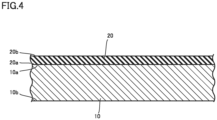
Fig. 4 is a cross-sectional view illustrating a buffer layer formation step S2; -
Fig. 5 is a cross-sectional view illustrating a solution application step S3; -
Fig. 6 is a cross-sectional view illustrating a first calcination step S4; and -
Fig. 7 is a cross-sectional view illustrating a second calcination step S5. - In the superconductive wire described in PTL 1, the oxide superconductive film is formed by the following method. Firstly, a raw material solution is prepared. The raw material solution contains chlorine and constituent elements of the oxide superconductive film. Secondly, the raw material solution is applied onto the buffer layer. Thirdly, a first calcination is performed. As a result, Ba2Cu3O4Cl4 is deposited on the surface of the buffer layer. Fourthly, a second calcination is performed. As a result, REBa2Cu3Ox crystals are formed on the buffer layer and grown while being oriented in a specific crystal orientation, thereby forming the oxide superconductive film. Ba2Cu3O4Cl4 assists in orienting the REBa2Cu3Ox crystals.
- In the superconductive wire described in PTL 1, chlorine is contained in the raw material solution, chlorine is also contained in the oxide superconductive film. Chlorine contained in the oxide superconductive film may disrupt the compositional balance of REBa2Cu3Ox or reduce the volume of the oxide superconductive film.
- The present disclosure has been made in view of the above-mentioned problem in the prior arts. An object of the present disclosure is to provide a superconductive wire with a reduced concentration of halogen in a superconductive layer.
- According to the present disclosure, a superconductive wire with a reduced concentration of halogen in a superconductive layer can be provided.
- First, embodiments of the present disclosure will be described.
- (1) A superconductive wire according to one embodiment includes a superconductive layer containing REBa2Cu3Ox. RE represents a rare earth element. The superconductive layer contains halogen. The concentration of halogen in the superconductive layer is less than 2000 ppm by mass. According to the superconductive wire of the above (1), it is possible to prevent the compositional balance of REBa2Cu3Ox contained in the superconductive layer from being disrupted and prevent the volume of the superconductive layer from being reduced.
- (2) In the superconductive wire of the above (1), the concentration of halogen in the superconductive layer may be 2 ppm or more by mass.
- (3) In the superconductive wire of the above (1) or (2), the halogen may be chlorine.
- (4) In the superconductive wire of any of the above (1) to (3), the superconductive layer may contain an alkali metal. The concentration of the alkali metal in the superconductive layer may be 1 ppb or more by mass.
- (5) In the superconductive wire of the above (4), the alkali metal may be sodium.
- (6) The superconductive wire of any one of the above (1) to (5) may further include a substrate and a buffer layer disposed on the substrate. The superconductive layer may have a first main surface and a second main surface opposite to the first main surface. The superconductive layer may be disposed on the buffer layer in such a manner that the first main surface faces the buffer layer. The amount of Ba2Cu3O4X2 precipitated on the second main surface may be greater than the amount of Ba2Cu3O4X2 precipitated in the superconductive layer. X represents halogen.
- (7) A method of manufacturing a superconductive wire according to one embodiment includes forming a superconductive layer composed of REBa2Cu3Ox on a buffer layer disposed on a substrate. RE represents a rare earth element. Forming the superconductive layer includes applying a solution containing a constituent element of the superconductive layer onto the buffer layer, forming a precursor of the superconductive layer by heating the applied solution, and forming the precursor into the superconductive layer by heating the precursor. The solution contains halogen. At least one of the solution, the precursor and the atmosphere in which the precursor is heated contains an alkali metal. According to the method of manufacturing a superconductive wire of the above (7), it is possible to reduce the concentration of halogen in the superconductive layer.
- (8) In the method of manufacturing a superconductive wire according to the above (7), the concentration of the alkali metal in the solution may be 1 ppb or more by mass.
- (9) In the method of manufacturing a superconductive wire according to the above (7), the partial pressure of the alkali metal in the atmosphere may be 1000 Pa or less.
- (10) In the method of manufacturing a superconductive wire according to any one of the above (7) to (9), the halogen may be chlorine.
- (11) In the method of manufacturing a superconductive wire according to any one of the above (7) to (10), the alkali metal may be sodium.
- Next, an embodiment of the present disclosure will be described in detail with reference to the drawings. In the following drawings, the same or corresponding parts are denoted by the same reference numerals, and the description thereof will not be repeated. The superconductive wire according to the embodiment will be denoted as a
superconductive wire 100. - The configuration of the
superconductive wire 100 will be described below with reference toFig. 1 . - As illustrated in
Fig. 1 , thesuperconductive wire 100 includes asubstrate 10, abuffer layer 20, and asuperconductive layer 30. Thesuperconductive wire 100 may further include a protective layer and a stabilizing layer. In this case, the constituent material of the protective layer is, for example, silver or a silver alloy, and the constituent material of the stabilizing layer is, for example, copper or a copper alloy. The protective layer is disposed on thesuperconductive layer 30. The stabilizing layer is disposed on the protective layer. - The
substrate 10 has amain surface 10a and amain surface 10b. Themain surface 10a and themain surface 10b are end surfaces in the thickness direction of thesubstrate 10. Themain surface 10b is opposite to themain surface 10a. - The
substrate 10 is, for example, a clad material that includes a tape member made of stainless steel, a copper (Cu) layer disposed on the tape member, and a nickel (Ni) layer disposed on the copper layer. The crystal axis of the copper layer is oriented. The crystal axis of the nickel layer is also oriented along the crystal axis of the copper layer. The nickel layer constitutes themain surface 10a. Thesubstrate 10 is not limited to the clad material described above, and may be a material other than the clad material. Thesubstrate 10 may be made of, for example, Hastelloy (registered trademark). Thesubstrate 10 may be a tape member made of a biaxially oriented metal material or a tape member made of a non-oriented metal material. - The
buffer layer 20 has amain surface 20a and amain surface 20b. Themain surface 20a and themain surface 20b are end surfaces in the thickness direction of thebuffer layer 20. Thebuffer layer 20 is disposed on thesubstrate 10 in such a manner that themain surface 20a is opposite to themain surface 10a (themain surface 20a faces themain surface 10a). - The
buffer layer 20 includes, for example, an yttria (Y2O3) layer, an yttria-stabilized zirconia (YSZ) layer disposed on the yttria layer, and a cerium oxide (CeO2) layer disposed on the yttria-stabilized zirconia layer. The structure of thebuffer layer 20 is not limited thereto. Since the crystal axis of the nickel layer of thesubstrate 10 is oriented as described above, the crystal axis of each layer in thebuffer layer 20 is also oriented. Thebuffer layer 20 may have a two-layer structure or a single-layer structure. - The
superconductive layer 30 is disposed on the buffer layer 20 (themain surface 20b). Since the crystal axis of thebuffer layer 20 is oriented as described above, the c-axis, i.e., the crystal axis of thesuperconductive layer 30 is also oriented along the crystal axis of thebuffer layer 20. Typically, thesuperconductive layer 30 is oriented such that the c-axis of the crystals of the constituent material (REBa2Cu3Ox to be described later) is oriented along the normal direction of themain surface 20b. In the present embodiment, "the c-axis is oriented along the normal direction of themain surface 20b" means that an inclination angle of the c-axis with respect to the normal direction of themain surface 20b is equal to or less than 15°. Thesuperconductive layer 30 has amain surface 30a and amain surface 30b. Themain surface 30a and themain surface 30b are end surfaces in the thickness direction of thesuperconductive layer 30. Themain surface 30a faces the buffer layer 20 (themain surface 20b). Themain surface 30b is opposite to themain surface 30a. - The constituent material of the
superconductive layer 30 is REBa2Cu3Ox. In the present embodiment, RE represents a rare earth element. The rare earth element is, for example, gadolinium (Gd), yttrium (Y), or eurobium (Eu). However, the rare earth element is not limited thereto. Thesuperconductive layer 30 contains halogen. The halogen is, for example, chlorine (Cl). However, halogen is not limited thereto. Thesuperconductive layer 30 may contain an alkali metal. The alkali metal is, for example, sodium (Na). However, the alkali metal is not limited thereto. Thesuperconductive layer 30 may not contain an alkali metal. - The concentration of halogen in the
superconductive layer 30 is less than 2000 ppm by mass. The concentration of halogen in thesuperconductive layer 30 may be 1800 ppm or less by mass or 1500 ppm or less by mass. The concentration of halogen in thesuperconductive layer 30 is, for example, 2 ppm or more by mass. The concentration of the alkali metal in thesuperconductive layer 30 is, for example, 2000 ppm or less by mass. The concentration of the alkali metal in thesuperconductive layer 30 is, for example, 1 ppb or more by mass. The concentration of halogen in thesuperconductive layer 30 and the concentration of alkali metal in thesuperconductive layer 30 are measured by ICP (Inductively Coupled Plasma) analysis, in other words, a method of dissolving thesuperconductive layer 30 in a solution and analyzing the concentration of ions in the solution. The concentration of halogen (or the alkali metal) in thesuperconductive layer 30 is the mass ratio of halogen (or the alkali metal) to the total mass of all elements contained in thesuperconductive layer 30. In other words, the total mass of all the elements constituting thesuperconductive layer 30 is 100 percent. - Ba2Cu3O4X2 may precipitate on the interface between the
superconductive layer 30 and themain surface 20b, in thesuperconductive layer 30, and on themain surface 30b. X represents halogen. The amount of Ba2Cu3O4X2 precipitated on themain surface 30b may be greater than the amount of Ba2Cu3O4X2 precipitated in thesuperconductive layer 30. - Hereinafter, a method of manufacturing the
superconductive wire 100 will be described with reference toFigs. 2 to 7 . - As illustrated in
Fig. 2 , the method of manufacturing thesuperconductive wire 100 includes a preparation step S1, a buffer layer formation step S2, a solution application step S3, a first calcination step S4, and a second calcination step S5. The buffer layer formation step S2 is performed after the preparation step S1. The solution application step S3 is performed after the buffer layer formation step S2. The first calcination step S4 is performed after the solution application step S3. The second calcination step S5 is performed after the first calcination step S4. - As illustrated in
Fig. 3 , in the preparation step S1, thesubstrate 10 is prepared. Thebuffer layer 20 is not disposed on thesubstrate 10 prepared in the preparation step S1. - As illustrated in
Fig. 4 , in the buffer layer formation step S2, thebuffer layer 20 is formed on thesubstrate 10. Thebuffer layer 20 is formed by sequentially forming the layers constituting thebuffer layer 20 by magnetron sputtering, for example. - The
superconductive layer 30 is formed by performing the solution application step S3, the first calcination step S4 and the second calcination step S5, in other words, by the MOD (Metal Organic Decomposition) method.Fig. 5 is a cross-sectional view illustrating the solution application step S3. As illustrated inFig. 5 , in the solution application step S3, acoating film 31 is formed on thebuffer layer 20. Thecoating film 31 is formed by applying a solution onto thebuffer layer 20 and drying the applied solution. - The solution contains a solvent and constituent elements of the
superconductive layer 30 solved in the solvent. The solution contains halogen and alkali metal. More specifically, the solution contains alcohol as the solvent, hydrochloric acid as the halogen source, sodium as the alkali metal, and rare earth elements, barium and copper as the constituent elements of thesuperconductive layer 30. The concentration of the alkali metal in the solution may be 1 ppb or more by mass. As an example, the halogen and the alkali metal may be contained in the solution by adding the halogen and the alkali metal to the solution. - As illustrated in
Fig. 6 , in the first calcination step S4, thecoating film 31 is heated to form acalcined film 32. Thecalcined film 32 is formed by a precursor of thesuperconductive layer 30. The precursor of thesuperconductive layer 30 may formed by a drying treatment for removing an organic solvent, a heat treatment for forming REBa2Cu3Ox nanocrystals, and another heat treatment for promoting decomposition of the raw material. The heating in the first calcination step S4 is performed in an atmosphere containing oxygen. - As illustrated in
Fig. 7 , in the second calcination step S5, thecalcined film 32 is heated to form thesuperconductive layer 30. The heating in the second calcination step S5 is performed in an atmosphere containing oxygen and at a temperature higher than that in the first calcination step S4. - When the heating in the second calcination step S5 is performed, the REBa2Cu3Ox crystals are epitaxially grown and oriented so that the c-axis thereof is along the normal direction of the
main surface 20b. While the heating in the second calcination step S5 is performed, there is a region where the epitaxial growth of REBa2Cu3Ox is unlikely to occur, and Ba2Cu3O4X2 precipitates in this region. Since the epitaxial growth of REBa2Cu3Ox is likely to occur around the precipitated Ba2Cu3O4X2, the orientation of REBa2Cu3Ox crystals is promoted by halogen contained in the solution. - By sequentially repeating the solution application step S3, the first calcination step S4, and the second calcination step S5, the film thickness of the
superconductive layer 30 becomes thicker, and thereby thesuperconductive wire 100 having the structure illustrated inFig. 1 is obtained. Since halogen is unevenly distributed in themain surface 30b of thesuperconductive layer 30 and the vicinity thereof as the solution application step S3, the first calcination step S4 and the second calcination step S5 are sequentially repeated, and as a result, when thesuperconductive layer 30 is formed by the MOD method using a solution containing halogen, the amount of Ba2Cu3O4X2 precipitated on themain surface 30b is larger than the amount of Ba2Cu3O4X2 precipitated in thesuperconductive layer 30. - In the above example, the solution containing the alkali metal is used, but the alkali metal may be contained in the atmosphere where the second calcination step S5 is performed instead of being contained in the solution. In this case, the partial pressure of the alkali metal in the atmosphere may be 1000 Pa or more. The gas constituting the atmosphere where the second calcination step S5 is performed may contain, for example, oxygen, an inert gas, and an alkali metal. The inert gas is, for example, argon or nitrogen. The pressure of the atmosphere is, for example, atmospheric pressure (101.3 kPa). The alkali metal may be contained in the
calcined film 32. As an example, the alkali metal may be contained in the atmosphere or thecalcined film 32 by adding the alkali metal to the atmosphere or thecalcined film 32. - As described above, since the alkali metal is contained in the solution used in the solution application step S3, the alkali metal is also contained in the
calcined film 32. During the heating in the second calcination step S5, the alkali metal in thecalcined film 32 is vaporized. The vaporized alkali metal reacts with chlorine in thesuperconductive layer 30, and is discharged to the outside. Therefore, in thesuperconductive wire 100, the concentration of halogen in thesuperconductive layer 30 is reduced to less than 2000 ppm by mass as compared with the case where no alkali metal is contained in the solution. The concentration of halogen in thesuperconductive layer 30 can be reduced to, for example, 1800 ppm or less by mass, or 1500 ppm or less by mass. - In the
superconductive wire 100, since the concentration of halogen in thesuperconductive layer 30 is reduced, it is possible to prevent the compositional balance of REBa2Cu3Ox constituting thesuperconductive layer 30 from being disrupted and prevent the volume of thesuperconductive layer 30 from being reduced. - In the
superconductive wire 100, since the alkali metal is contained in the solution used in the solution application step S3, the alkali metal may remain in thesuperconductive layer 30; but even if the alkali metal remains in thesuperconductive layer 30, the alkali metal is unlikely to adversely affect the superconductive characteristics of thesuperconductive layer 30. The concentration of halogen in thesuperconductive layer 30 can be similarly reduced not only in the case when the alkali metal is contained in the solution used in the solution application step S3 but also in the case when the alkali metal is contained in thecalcined film 32 or the atmosphere in the second calcination step S5. - It should be understood that the embodiments disclosed herein have been presented for the purpose of illustration and description but not limited in all aspects. It is intended that the scope of the present invention is not limited to the description above but defined by the scope of the claims and encompasses all modifications equivalent in meaning and scope to the claims.
- 10: substrate; 10a, 10b: main surface; 20: buffer layer; 20a, 20b: main surface; 30: superconductive layer; 30a, 30b: main surface; 31: coating film; 32: calcined film; 100: superconductive wire; S1: preparation step; S2: buffer layer formation step; S3: solution application step; S4: first calcination step; S5: second calcination step.
Claims (11)
- A superconductive wire comprising:a superconductive layer containing REBa2Cu3Ox,wherein RE represents a rare earth element,the superconductive layer contains halogen, andthe concentration of the halogen in the superconductive layer is less than 2000 ppm by mass.
- The superconductive wire according to claim 1, wherein
the concentration of the halogen in the superconductive layer is 2 ppm or more by mass. - The superconductive wire according to claim 1 or claim 2, wherein
the halogen is chlorine. - The superconductive wire according to any one of claims 1 to 3, whereinthe superconductive layer contains an alkali metal, andthe concentration of the alkali metal in the superconductive layer is 1 ppb or more by mass.
- The superconductive wire according to claim 4, wherein
the alkali metal is sodium. - The superconductive wire according to any one of claims 1 to 5, further comprising:a substrate; anda buffer layer disposed on the substrate,wherein the superconductive layer has a first main surface and a second main surface opposite to the first main surface,the superconductive layer is disposed on the buffer layer in such a manner that the first main surface faces the buffer layer,an amount of Ba2Cu3O4X2 precipitated on the second main surface is greater than an amount of Ba2Cu3O4X2 precipitated in the superconductive layer, andX represents halogen.
- A method of manufacturing a superconductive wire, comprising:a step of forming a superconductive layer composed of REBa2Cu3Ox on a buffer layer disposed on a substrate,wherein RE represents a rare earth element,forming the superconductive layer includes applying a solution containing a constituent element of the superconductive layer onto the buffer layer, forming a precursor of the superconductive layer by heating the applied solution, and forming the precursor into the superconductive layer by heating the precursor,the solution contains halogen, andat least one of the solution, the precursor and an atmosphere in which the precursor is heated contains an alkali metal.
- The method of manufacturing a superconductive wire according to claim 7, wherein
the concentration of the alkali metal in the solution is 1 ppb or more by mass. - The method of manufacturing a superconductive wire according to claim 7 or 8, wherein
the partial pressure of the alkali metal in the atmosphere is 1000 Pa or less. - The method of manufacturing a superconductive wire according to any one of claims 7 to 9, wherein
the halogen is chlorine. - The method of manufacturing a superconductive wire according to any one of claims 7 to 10, wherein
the alkali metal is sodium.
Applications Claiming Priority (2)
| Application Number | Priority Date | Filing Date | Title |
|---|---|---|---|
| JP2023040888 | 2023-03-15 | ||
| PCT/JP2024/008820 WO2024190614A1 (en) | 2023-03-15 | 2024-03-07 | Superconducting wire material and production method for superconducting wire material |
Publications (2)
| Publication Number | Publication Date |
|---|---|
| EP4513514A1 true EP4513514A1 (en) | 2025-02-26 |
| EP4513514A4 EP4513514A4 (en) | 2025-10-22 |
Family
ID=92755713
Family Applications (1)
| Application Number | Title | Priority Date | Filing Date |
|---|---|---|---|
| EP24770720.1A Pending EP4513514A4 (en) | 2023-03-15 | 2024-03-07 | SUPERCONDUCTING WIRE MATERIAL AND MANUFACTURING METHOD FOR SUPERCONDUCTING WIRE MATERIAL |
Country Status (5)
| Country | Link |
|---|---|
| US (1) | US20250364157A1 (en) |
| EP (1) | EP4513514A4 (en) |
| JP (1) | JP7754367B2 (en) |
| CN (1) | CN119278490A (en) |
| WO (1) | WO2024190614A1 (en) |
Family Cites Families (5)
| Publication number | Priority date | Publication date | Assignee | Title |
|---|---|---|---|---|
| JP3288824B2 (en) * | 1992-09-29 | 2002-06-04 | キヤノン株式会社 | Production method of metal oxide |
| JP5740795B2 (en) | 2011-12-09 | 2015-07-01 | 住友電気工業株式会社 | Manufacturing method of oxide superconducting wire |
| JP2014207056A (en) | 2013-04-10 | 2014-10-30 | 住友電気工業株式会社 | Method for manufacturing an oxide superconductive wire and oxide superconductive wire |
| JP6136073B2 (en) | 2013-12-02 | 2017-05-31 | 住友電気工業株式会社 | Oxide superconducting thin film and manufacturing method thereof, and oxide superconducting thin film wire |
| JP7748235B2 (en) | 2021-09-10 | 2025-10-02 | キヤノン株式会社 | Server, its control method, and program |
-
2024
- 2024-03-07 US US18/868,018 patent/US20250364157A1/en active Pending
- 2024-03-07 EP EP24770720.1A patent/EP4513514A4/en active Pending
- 2024-03-07 CN CN202480002756.1A patent/CN119278490A/en active Pending
- 2024-03-07 WO PCT/JP2024/008820 patent/WO2024190614A1/en not_active Ceased
- 2024-03-07 JP JP2025506775A patent/JP7754367B2/en active Active
Also Published As
| Publication number | Publication date |
|---|---|
| JP7754367B2 (en) | 2025-10-15 |
| US20250364157A1 (en) | 2025-11-27 |
| WO2024190614A1 (en) | 2024-09-19 |
| CN119278490A (en) | 2025-01-07 |
| EP4513514A4 (en) | 2025-10-22 |
| JPWO2024190614A1 (en) | 2024-09-19 |
Similar Documents
| Publication | Publication Date | Title |
|---|---|---|
| CN1208850C (en) | Enhanced Coated High-Temperature Superconductors | |
| CN101911218B (en) | Re-based oxide superconducting wire and manufacturing method thereof | |
| US4940693A (en) | High temperature superconducting thin film structure and method of making | |
| US9082530B2 (en) | Superconducting thin film material and method of manufacturing same | |
| CN101652505A (en) | Polycrystalline thin film, method for producing the same, and oxide superconducting conductor | |
| JP2002203439A (en) | Tape-shaped oxide superconductor | |
| CN102870244B (en) | The formation of thick oxide films of single coating | |
| CN103635978A (en) | Superconducting wire | |
| WO2007135831A1 (en) | Superconducting thin film material and method for producing superconducting thin film material | |
| CN102834879B (en) | Oxide superconducting conductor and production method therefor | |
| CN105684103B (en) | Oxide superconducting wire and method for producing oxide superconducting wire | |
| EP4513514A1 (en) | Superconducting wire material and production method for superconducting wire material | |
| EP2000566A2 (en) | Interlayer of orientational substrate and orientational substrate for forming epitaxial film | |
| CN112469668A (en) | Oxide superconducting wire and method for producing same | |
| CN102473487B (en) | Substrate, method of producing substrate, superconducting wire and method of producing of superconducting wire | |
| EP2477193B1 (en) | Tape base for superconducting wire, and superconducting wire | |
| CN101385097B (en) | Manufacturing method of superconducting thin film material, superconducting device and superconducting thin film material | |
| RU2481673C1 (en) | Method to manufacture thin-film high-temperature superconductive material | |
| EP2372722B1 (en) | Method for manufacturing precursor, method for manufacturing superconducting wire, precursor, and superconducting wire | |
| JP2005276465A (en) | Superconducting wire | |
| WO2013008851A1 (en) | Superconducting thin film and method for manufacturing superconducting thin film | |
| EP4485484A1 (en) | Superconducting wire material | |
| US20240188452A1 (en) | Joined body and method for producing joined body | |
| WO2012111678A1 (en) | Super-conducting wire and method for producing super-conducting wire | |
| JP2010123433A (en) | Method of manufacturing re123 superconducting thin film wire rod, and re123 superconducting thin film wire rod |
Legal Events
| Date | Code | Title | Description |
|---|---|---|---|
| STAA | Information on the status of an ep patent application or granted ep patent |
Free format text: STATUS: THE INTERNATIONAL PUBLICATION HAS BEEN MADE |
|
| PUAI | Public reference made under article 153(3) epc to a published international application that has entered the european phase |
Free format text: ORIGINAL CODE: 0009012 |
|
| STAA | Information on the status of an ep patent application or granted ep patent |
Free format text: STATUS: REQUEST FOR EXAMINATION WAS MADE |
|
| 17P | Request for examination filed |
Effective date: 20241119 |
|
| AK | Designated contracting states |
Kind code of ref document: A1 Designated state(s): AL AT BE BG CH CY CZ DE DK EE ES FI FR GB GR HR HU IE IS IT LI LT LU LV MC ME MK MT NL NO PL PT RO RS SE SI SK SM TR |
|
| REG | Reference to a national code |
Ref country code: DE Ref legal event code: R079 Free format text: PREVIOUS MAIN CLASS: H01B0012060000 Ipc: H10N0060010000 |
|
| A4 | Supplementary search report drawn up and despatched |
Effective date: 20250919 |
|
| RIC1 | Information provided on ipc code assigned before grant |
Ipc: H10N 60/01 20230101AFI20250915BHEP Ipc: H10N 60/20 20230101ALI20250915BHEP Ipc: H10N 60/85 20230101ALI20250915BHEP Ipc: H01B 12/06 20060101ALN20250915BHEP |
|
| RIC1 | Information provided on ipc code assigned before grant |
Ipc: H10N 60/01 20230101AFI20251205BHEP Ipc: H10N 60/20 20230101ALI20251205BHEP Ipc: H10N 60/85 20230101ALI20251205BHEP Ipc: H01B 12/06 20060101ALN20251205BHEP |
|
| GRAP | Despatch of communication of intention to grant a patent |
Free format text: ORIGINAL CODE: EPIDOSNIGR1 |
|
| STAA | Information on the status of an ep patent application or granted ep patent |
Free format text: STATUS: GRANT OF PATENT IS INTENDED |
|
| GRAJ | Information related to disapproval of communication of intention to grant by the applicant or resumption of examination proceedings by the epo deleted |
Free format text: ORIGINAL CODE: EPIDOSDIGR1 |
|
| STAA | Information on the status of an ep patent application or granted ep patent |
Free format text: STATUS: REQUEST FOR EXAMINATION WAS MADE |
|
| DAV | Request for validation of the european patent (deleted) | ||
| DAX | Request for extension of the european patent (deleted) | ||
| GRAP | Despatch of communication of intention to grant a patent |
Free format text: ORIGINAL CODE: EPIDOSNIGR1 |
|
| STAA | Information on the status of an ep patent application or granted ep patent |
Free format text: STATUS: GRANT OF PATENT IS INTENDED |
|
| INTC | Intention to grant announced (deleted) | ||
| RIC1 | Information provided on ipc code assigned before grant |
Ipc: H10N 60/01 20230101AFI20260211BHEP Ipc: H10N 60/20 20230101ALI20260211BHEP Ipc: H10N 60/85 20230101ALI20260211BHEP Ipc: H01B 12/06 20060101ALN20260211BHEP |
|
| INTG | Intention to grant announced |
Effective date: 20260312 |