EP4513476A1 - Backlight module and display apparatus - Google Patents
Backlight module and display apparatus Download PDFInfo
- Publication number
- EP4513476A1 EP4513476A1 EP22931225.1A EP22931225A EP4513476A1 EP 4513476 A1 EP4513476 A1 EP 4513476A1 EP 22931225 A EP22931225 A EP 22931225A EP 4513476 A1 EP4513476 A1 EP 4513476A1
- Authority
- EP
- European Patent Office
- Prior art keywords
- sub
- pixel
- data line
- voltage
- gray scale
- Prior art date
- Legal status (The legal status is an assumption and is not a legal conclusion. Google has not performed a legal analysis and makes no representation as to the accuracy of the status listed.)
- Pending
Links
Images


Classifications
-
- G—PHYSICS
- G09—EDUCATION; CRYPTOGRAPHY; DISPLAY; ADVERTISING; SEALS
- G09G—ARRANGEMENTS OR CIRCUITS FOR CONTROL OF INDICATING DEVICES USING STATIC MEANS TO PRESENT VARIABLE INFORMATION
- G09G3/00—Control arrangements or circuits, of interest only in connection with visual indicators other than cathode-ray tubes
- G09G3/20—Control arrangements or circuits, of interest only in connection with visual indicators other than cathode-ray tubes for presentation of an assembly of a number of characters, e.g. a page, by composing the assembly by combination of individual elements arranged in a matrix no fixed position being assigned to or needed to be assigned to the individual characters or partial characters
- G09G3/34—Control arrangements or circuits, of interest only in connection with visual indicators other than cathode-ray tubes for presentation of an assembly of a number of characters, e.g. a page, by composing the assembly by combination of individual elements arranged in a matrix no fixed position being assigned to or needed to be assigned to the individual characters or partial characters by control of light from an independent source
- G09G3/3406—Control of illumination source
-
- G—PHYSICS
- G09—EDUCATION; CRYPTOGRAPHY; DISPLAY; ADVERTISING; SEALS
- G09G—ARRANGEMENTS OR CIRCUITS FOR CONTROL OF INDICATING DEVICES USING STATIC MEANS TO PRESENT VARIABLE INFORMATION
- G09G3/00—Control arrangements or circuits, of interest only in connection with visual indicators other than cathode-ray tubes
- G09G3/20—Control arrangements or circuits, of interest only in connection with visual indicators other than cathode-ray tubes for presentation of an assembly of a number of characters, e.g. a page, by composing the assembly by combination of individual elements arranged in a matrix no fixed position being assigned to or needed to be assigned to the individual characters or partial characters
- G09G3/2007—Display of intermediate tones
- G09G3/2074—Display of intermediate tones using sub-pixels
-
- G—PHYSICS
- G09—EDUCATION; CRYPTOGRAPHY; DISPLAY; ADVERTISING; SEALS
- G09G—ARRANGEMENTS OR CIRCUITS FOR CONTROL OF INDICATING DEVICES USING STATIC MEANS TO PRESENT VARIABLE INFORMATION
- G09G3/00—Control arrangements or circuits, of interest only in connection with visual indicators other than cathode-ray tubes
- G09G3/20—Control arrangements or circuits, of interest only in connection with visual indicators other than cathode-ray tubes for presentation of an assembly of a number of characters, e.g. a page, by composing the assembly by combination of individual elements arranged in a matrix no fixed position being assigned to or needed to be assigned to the individual characters or partial characters
- G09G3/22—Control arrangements or circuits, of interest only in connection with visual indicators other than cathode-ray tubes for presentation of an assembly of a number of characters, e.g. a page, by composing the assembly by combination of individual elements arranged in a matrix no fixed position being assigned to or needed to be assigned to the individual characters or partial characters using controlled light sources
- G09G3/30—Control arrangements or circuits, of interest only in connection with visual indicators other than cathode-ray tubes for presentation of an assembly of a number of characters, e.g. a page, by composing the assembly by combination of individual elements arranged in a matrix no fixed position being assigned to or needed to be assigned to the individual characters or partial characters using controlled light sources using electroluminescent panels
- G09G3/32—Control arrangements or circuits, of interest only in connection with visual indicators other than cathode-ray tubes for presentation of an assembly of a number of characters, e.g. a page, by composing the assembly by combination of individual elements arranged in a matrix no fixed position being assigned to or needed to be assigned to the individual characters or partial characters using controlled light sources using electroluminescent panels semiconductive, e.g. using light-emitting diodes [LED]
-
- G—PHYSICS
- G09—EDUCATION; CRYPTOGRAPHY; DISPLAY; ADVERTISING; SEALS
- G09G—ARRANGEMENTS OR CIRCUITS FOR CONTROL OF INDICATING DEVICES USING STATIC MEANS TO PRESENT VARIABLE INFORMATION
- G09G3/00—Control arrangements or circuits, of interest only in connection with visual indicators other than cathode-ray tubes
- G09G3/20—Control arrangements or circuits, of interest only in connection with visual indicators other than cathode-ray tubes for presentation of an assembly of a number of characters, e.g. a page, by composing the assembly by combination of individual elements arranged in a matrix no fixed position being assigned to or needed to be assigned to the individual characters or partial characters
- G09G3/34—Control arrangements or circuits, of interest only in connection with visual indicators other than cathode-ray tubes for presentation of an assembly of a number of characters, e.g. a page, by composing the assembly by combination of individual elements arranged in a matrix no fixed position being assigned to or needed to be assigned to the individual characters or partial characters by control of light from an independent source
- G09G3/3406—Control of illumination source
- G09G3/3413—Details of control of colour illumination sources
-
- G—PHYSICS
- G09—EDUCATION; CRYPTOGRAPHY; DISPLAY; ADVERTISING; SEALS
- G09G—ARRANGEMENTS OR CIRCUITS FOR CONTROL OF INDICATING DEVICES USING STATIC MEANS TO PRESENT VARIABLE INFORMATION
- G09G3/00—Control arrangements or circuits, of interest only in connection with visual indicators other than cathode-ray tubes
- G09G3/20—Control arrangements or circuits, of interest only in connection with visual indicators other than cathode-ray tubes for presentation of an assembly of a number of characters, e.g. a page, by composing the assembly by combination of individual elements arranged in a matrix no fixed position being assigned to or needed to be assigned to the individual characters or partial characters
- G09G3/34—Control arrangements or circuits, of interest only in connection with visual indicators other than cathode-ray tubes for presentation of an assembly of a number of characters, e.g. a page, by composing the assembly by combination of individual elements arranged in a matrix no fixed position being assigned to or needed to be assigned to the individual characters or partial characters by control of light from an independent source
- G09G3/3406—Control of illumination source
- G09G3/342—Control of illumination source using several illumination sources separately controlled corresponding to different display panel areas, e.g. along one dimension such as lines
- G09G3/3426—Control of illumination source using several illumination sources separately controlled corresponding to different display panel areas, e.g. along one dimension such as lines the different display panel areas being distributed in two dimensions, e.g. matrix
-
- G—PHYSICS
- G09—EDUCATION; CRYPTOGRAPHY; DISPLAY; ADVERTISING; SEALS
- G09G—ARRANGEMENTS OR CIRCUITS FOR CONTROL OF INDICATING DEVICES USING STATIC MEANS TO PRESENT VARIABLE INFORMATION
- G09G2300/00—Aspects of the constitution of display devices
- G09G2300/02—Composition of display devices
- G09G2300/023—Display panel composed of stacked panels
-
- G—PHYSICS
- G09—EDUCATION; CRYPTOGRAPHY; DISPLAY; ADVERTISING; SEALS
- G09G—ARRANGEMENTS OR CIRCUITS FOR CONTROL OF INDICATING DEVICES USING STATIC MEANS TO PRESENT VARIABLE INFORMATION
- G09G2300/00—Aspects of the constitution of display devices
- G09G2300/04—Structural and physical details of display devices
- G09G2300/0439—Pixel structures
- G09G2300/0452—Details of colour pixel setup, e.g. pixel composed of a red, a blue and two green components
-
- G—PHYSICS
- G09—EDUCATION; CRYPTOGRAPHY; DISPLAY; ADVERTISING; SEALS
- G09G—ARRANGEMENTS OR CIRCUITS FOR CONTROL OF INDICATING DEVICES USING STATIC MEANS TO PRESENT VARIABLE INFORMATION
- G09G2320/00—Control of display operating conditions
- G09G2320/02—Improving the quality of display appearance
- G09G2320/0233—Improving the luminance or brightness uniformity across the screen
-
- G—PHYSICS
- G09—EDUCATION; CRYPTOGRAPHY; DISPLAY; ADVERTISING; SEALS
- G09G—ARRANGEMENTS OR CIRCUITS FOR CONTROL OF INDICATING DEVICES USING STATIC MEANS TO PRESENT VARIABLE INFORMATION
- G09G2320/00—Control of display operating conditions
- G09G2320/02—Improving the quality of display appearance
- G09G2320/0242—Compensation of deficiencies in the appearance of colours
-
- G—PHYSICS
- G09—EDUCATION; CRYPTOGRAPHY; DISPLAY; ADVERTISING; SEALS
- G09G—ARRANGEMENTS OR CIRCUITS FOR CONTROL OF INDICATING DEVICES USING STATIC MEANS TO PRESENT VARIABLE INFORMATION
- G09G2320/00—Control of display operating conditions
- G09G2320/06—Adjustment of display parameters
- G09G2320/0626—Adjustment of display parameters for control of overall brightness
- G09G2320/0646—Modulation of illumination source brightness and image signal correlated to each other
-
- G—PHYSICS
- G09—EDUCATION; CRYPTOGRAPHY; DISPLAY; ADVERTISING; SEALS
- G09G—ARRANGEMENTS OR CIRCUITS FOR CONTROL OF INDICATING DEVICES USING STATIC MEANS TO PRESENT VARIABLE INFORMATION
- G09G2360/00—Aspects of the architecture of display systems
- G09G2360/16—Calculation or use of calculated indices related to luminance levels in display data
Definitions
- the present application relates to the field of displaying technologies, and in particular, to a backlight module and a display device.
- a display device includes a backlight module and a display panel.
- the display panel includes a plurality of scan lines, a plurality of data lines, a plurality of sub-pixels, and a plurality of switch circuits in a one-to-one correspondence with the plurality of sub-pixels.
- the backlight module provides light sources for the plurality of sub-pixels on the display panel.
- the scan line controls the switch circuit to be on, and the data line writes a data voltage to the corresponding sub-pixel through the switch circuit, so as to charge the sub-pixel and make the sub-pixel emit light.
- the plurality of scan lines when the display device displays a frame of image, the plurality of scan lines, starting from the first one, output scan signals one by one to control the plurality of sub-pixels to emit light row by row.
- the polarity of the data voltage output by each data line with respect to the common voltage remains unchanged.
- One objective of the embodiments of the present application is to provide a backlight module and a display device that can solve the problem of non-uniformity of brightness of the display panel in the related art.
- a backlight module is provided.
- the backlight module is applied to a display device including a display panel, where the display panel includes a plurality of sub-pixels and M data lines; and each of the M data lines is connected to at least two of the plurality of sub-pixels, M being an integer greater than 3;
- the backlight module further includes a plurality of drive circuits corresponding to the plurality of light-emitting elements, respectively; and each of the plurality of drive circuits has a first input terminal connected to an output terminal of a power supply (32) and an output terminal connected to the corresponding light-emitting element; and each of the plurality of drive circuits further has a second input terminal connected to the controller; and the controller is further configured to control the brightness of each of the plurality of light-emitting elements by controlling a drive current output by each of the plurality of drive circuits to the corresponding light-emitting element.
- each of the plurality of drive circuits includes a first transistor, a second transistor, and a capacitor;
- the controller stores a first correspondence relationship, which is a correspondence between the target gray scale and a first voltage; and the controller is configured to: obtain, when the j-th sub-pixel connected to the i-th data line does not emit light, the corresponding first voltage from the first correspondence relationship according to the target gray scale of the (j+1)-th sub-pixel connected to the i-th data line, and input a voltage to the input terminal of the second transistor of the drive circuit corresponding to the (j+1)-th sub-pixel connected to the i-th data line according to the first voltage; and the controller further stores a second correspondence relationship, which is a correspondence between the target gray scale and a second voltage; the first voltage corresponding to any target gray scale in the first correspondence relationship is greater than the second voltage corresponding to the any target gray scale in the second correspondence relationship; and the controller is configured to: obtain, when the j-th sub-pixel connected to the i-th data line emits light, the corresponding second voltage from the second correspondence relationship according to the target gray scale of the (j
- a difference between the first voltage and the second voltage increases by 0.15V each time when the target gray scale increases by 1; when the target gray scale is greater than 8 and less than or equal to 20, the difference value between the first voltage and the second voltage increases by 0.02V each time when the target gray scale increases by 1; when the target gray scale is greater than 20 and less than or equal to 220, the difference value between the first voltage and the second voltage increases by 0.01V each time when the target gray scale increases by 1; when the target gray scale is greater than 220 and less than or equal to 225, the difference value between the first voltage and the second voltage increases by 0.02V each time when the target gray scale increases by 1; when the target gray scale is greater than 225 and less than or equal to 238, the difference value between the first voltage and the second voltage increases by 0.03V each time when the target gray scale increases by 1; when the target gray scale is greater than 238 and less than or equal to 244, the difference value between the first voltage and
- the controller controls a third brightness to be equal to the first brightness; the third brightness is the brightness of the light-emitting element corresponding to the p-th sub-pixel connected to the first data line; p is a positive integer; and a color of the p-th sub-pixel connected to the first data line is the same as a color of the (j+1)-th sub-pixel connected to the i-th data line.
- the controller controls a fourth brightness to be equal to the first brightness; the fourth brightness is the brightness of the light-emitting element corresponding to the p-th sub-pixel connected to the M-th data line; p is a positive integer; and a color of the p-th sub-pixel connected to the M-th data line is the same as a color of the (j+1)-th sub-pixel connected to the i-th data line.
- each of the plurality of light-emitting elements is a sub-millimeter light-emitting diode (mini LED) or a micro light-emitting diode (micro LED).
- mini LED sub-millimeter light-emitting diode
- micro LED micro light-emitting diode
- a display device includes a display panel and the backlight module according to the first aspect; the display panel includes a plurality of sub-pixels and M data lines; and each of the M data lines is connected to at least two of the plurality of sub-pixels, M is an integer greater than 3.
- the plurality of sub-pixels are arranged in N rows and M-1 columns, and j is a positive integer less than or equal to N-1; and the first data line of the M data lines is connected to a first sub-pixel in an odd-numbered row, the M-th data line is connected to an (M-1)-th sub-pixel in an even-numbered row, and the i-th data line is connected to an i-th sub-pixel in the odd-numbered row and an (i-1)-th sub-pixel in the even-numbered row.
- the backlight module includes the plurality of light-emitting elements and the controller.
- the plurality of light-emitting elements are served as light sources for the plurality of sub-pixels respectively.
- the controller is configured to control the brightness of each of the light-emitting elements.
- the controller is configured to control the first brightness to be greater than the second brightness.
- the first brightness is the brightness of the light-emitting element corresponding to the (j+1)-th sub-pixel connected to the i-th data line when a j-th sub-pixel connected to the i-th data line does not emit light.
- the second brightness is the brightness of the light-emitting element corresponding to the (j+1)-th sub-pixel connected to the i-th data line when the j-th sub-pixel connected to the i-th data line emits light. That is, if the i-th data line does not need to charge one of the plurality of sub-pixels connected to the i-th data line, when the next sub-pixel emits light, the controller increases the brightness of the light-emitting element corresponding to the next sub-pixel. In this way, the next sub-pixel can have the actual gray scale that reaches the target gray scale thereof, so that the uniformity of brightness of the display panel is improved.
- the backlight module is applied to a display device, which includes the backlight module and the display panel.
- the display panel includes a plurality of sub-pixels, a plurality of switch circuits, a plurality of scan lines, and a plurality of data lines.
- the number of the switch circuits is equal to the number of the sub-pixels, and the plurality of switch circuits are connected to the plurality of sub-pixels in a one-to-one correspondence manner.
- Each switch circuit has an input terminal, an output terminal, and a control terminal.
- the control terminal of the switch circuit is configured to control the connection and disconnection between the input terminal and the output terminal of the switch circuit.
- Each of the plurality of switch circuits has the input terminal connected to one data line, the control terminal connected to one scan line, and the output terminal connected to the corresponding sub-pixel.
- a scan line outputs a scan signal
- all switch circuits connected to the scan line are on.
- a switch circuit is on, a data voltage in the data line is output by the switch circuit to the sub-pixel connected to the switch circuit.
- each sub-pixel may include a pixel electrode, and may further include a color resist located on the pixel electrode.
- the pixel electrode is configured to form a voltage difference with a common electrode.
- a liquid crystal is provided between the pixel electrode and the common electrode.
- FIG. 1 is a structural diagram of a display panel 10 according to the present application.
- the display panel 10 includes 36 sub-pixels 110, 36 switch circuits 120, 4 scan lines 140, and 10 data lines 130.
- the 36 sub-pixels 110 are arranged in 4 rows and 9 columns, and the 36 sub-pixels 110 include 12 red (R) sub-pixels, 12 green (G) sub-pixels, and 12 blue (B) sub-pixels.
- the switch circuits 120 and the sub-pixels 110 are in a one-to-one correspondence, and the output terminal of each switch circuit 120 is connected to the corresponding sub-pixel 110.
- the 10 data lines 130 are denoted as S1, S2...
- Each data line 130 extends in the column direction, and each scan line 140 extends in the row direction.
- the control terminals of the switch circuits 120 corresponding to the sub-pixels 110 in the first row are connected to G1.
- the control terminals of the switch circuits 120 corresponding to the sub-pixels 110 in the second row are connected to G2.
- the connection relationships of other control terminals can be deduced in the same way.
- S1 is connected to the input terminals of the switch circuits 120 corresponding to the first sub-pixels 110 in the odd-numbered rows (the first and third rows).
- S10 is connected to the input terminals of the switch circuits 120 corresponding to the ninth sub-pixels 110 in the even-numbered rows (the second and fourth rows).
- Si is connected to the input terminal of the switch circuit 120 corresponding to the i-th sub-pixel 110 in the odd-numbered row and the input terminal of the switch circuit 120 corresponding to the (i-1)-th sub-pixel 110 in the even-numbered row.
- Si refers to the i-th data line 130 from left to right along the paper, and i is an integer greater than 1 and less than 10, such as 2, 3, 4 or 9.
- G1, G2, G3, and G4 successively output scan signals.
- G1 outputs the scan signal
- the switch circuits 120 corresponding to the sub-pixels 110 in the first row are all on.
- S1 to S9 output data voltages to charge all the sub-pixels 110 in the first row, such that all the sub-pixels 110 in the first row emit light.
- G2 outputs the scan signal
- the switch circuits 120 corresponding to the sub-pixels 110 in the second row are all on.
- S2 to S10 output data voltages to charge all the sub-pixels 110 in the second row, such that all the sub-pixels 110 in the second row emit light.
- the switch circuits 120 corresponding to the sub-pixels 110 in the fourth row are all on.
- S2 to S10 output data voltages to charge all the sub-pixels 110 in the fourth row, such that all the sub-pixels 110 in the fourth row emit light.
- the polarity of the data voltage output by each data line 130 with respect to a common voltage remains unchanged.
- the polarity of the data voltage output by each data line 130 with respect to the common voltage may change.
- the common voltage is 0 V
- the display panel 10 is configured to display a solid color image (each sub-pixel 110 has the same gray scale).
- the data voltage output by S1 when the first frame image is displayed, the data voltage output by S1 may be fixed to 7 V, the data voltage output by S2 may be fixed to -7 V, the data voltage output by S3 may be fixed to 7 V, ..., and similarly, the data voltage output by S10 may be fixed to -7 V.
- the data voltage output by S1 when the second frame image is displayed, the data voltage output by S1 may be fixed to -7 V, the data voltage output by S2 may be fixed to 7 V, the data voltage output by S3 may be fixed to -7 V, ..., and similarly, the data voltage output by S10 may be fixed to 7 V.
- some sub-pixels 110 in the display panel 10 do not emit light, that is, the data lines 130 do not need to charge some sub-pixels 110.
- the display panel 10 is configured to display a B-G frame
- all R sub-pixels in the display panel 10 do not emit light.
- S3 outputs the data voltage (e.g., 7 V) to the third sub-pixel 110 in the first row, that is, the B sub-pixel.
- S3 When G2 outputs the scan signal, S3 outputs the data voltage (e.g., 7 V) to the second sub-pixel 110 in the second row, that is, the G sub-pixel.
- the voltage in S3 is always 7 V. In other words, in this process, the data voltage to be written by the second sub-pixel 110 in the second row does not need to rise from 0 V to 7 V.
- S5 When G2 outputs the scan signal, S5 does not need to output the data voltage to the fourth sub-pixel 110 in the second row, that is, the R sub-pixel. At this time, the voltage in S5 is 0.
- S5 When G3 outputs the scan signal, S5 needs to output the data voltage (e.g., 7 V) to the fifth sub-pixel 110 in the third row, that is, the G sub-pixel.
- the voltage in S5 When G3 outputs the scan signal, the voltage in S5 needs to rise from 0 V to 7 V. In other words, in this process, the data voltage to be written by the fifth sub-pixel 110 in the third row needs to rise from 0 V to 7 V. In this case, the charging amount of the fifth sub-pixel 110 in the third row must be lower than that of the second sub-pixel 110 of the same color in the second row.
- FIG. 2 is a structural diagram of a display device 30 provided by the first embodiment of the present application from a first perspective (data lines are not shown in the figure).
- FIG. 3 is a structural diagram of the display device 30 provided by the first embodiment of the present application from a second perspective (data lines and scan lines except G1 are not shown in the figure).
- the first perspective and the second perspective are two different perspectives.
- the display device 30 includes a backlight module 20 and the display panel 10 as described above.
- the backlight module 20 includes a plurality of light-emitting elements 210 and a controller 220 (not shown in the figures).
- the number of the light-emitting elements 210 is equal to the number of the sub-pixels 110 of the display panel 10.
- the controller 220 increases the brightness of the light-emitting element 210 corresponding to the next sub-pixel 110.
- the j-th sub-pixel 110 and the (j+1)-th sub-pixel 110 connected to the i-th data line 130 are arranged from top to bottom along the paper. It is understandable that in the embodiment shown in FIG. 1 , M is equal to 10. In other embodiments not shown, M can be any integer greater than 2, such as 10, 13 or 7. In some specific embodiments, M is equal to 5761. i is an integer greater than 1 and less than M, and j is a positive integer.
- the charging amount of the (j+1)-th sub-pixel 110 cannot reach the one required for light emission. That is, the voltage of the pixel electrode cannot reach the voltage required for light emission. As a result, the rotation angle of the liquid crystal is small, thereby leading to a low brightness of the (j+1)-th sub-pixel 110.
- controller 220 for controlling the brightness of the light-emitting element 210 is described below.
- the controller 220 can control the brightness of each light-emitting element 210 by controlling a drive current output by each drive circuit 230 to the corresponding light-emitting element 210.
- a greater drive current output by the drive circuit 230 to the corresponding light-emitting element 210 can lead to a higher brightness of the corresponding light-emitting element 210.
- the controller 220 controls the drive current output by the drive circuit 230 corresponding to the light-emitting element 210 corresponding to the (j+1)-th sub-pixel 110 connected to the i-th data line 130 when the j-th sub-pixel 110 connected to the i-th data line 130 does not emit light to be greater than the drive current output by the drive circuit 230 corresponding to the light-emitting element 210 corresponding to the (j+1)-th sub-pixel 110 connected to the i-th data line 130 when the j-th sub-pixel 110 connected to the i-th data line 130 emits light.
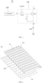
- FIG. 5 is a circuit configuration of the drive circuit 230 provided by the second embodiment of the present application.
- the drive circuit 230 may include a first transistor TFT1, a second transistor TFT2, and a capacitor C.
- the first transistor TFT1 and the second transistor TFT2 are thin film transistors (Thin Film Transistors, TFTs).
- An input terminal of the first transistor TFT1 is connected to the output terminal a of the power supply 32. That is, the input terminal of the first transistor TFT1 forms the first input terminal b of the drive circuit 230.
- An output terminal of the first transistor TFT1 is connected to the light-emitting element 210 corresponding to the drive circuit 230.
- the working process of the drive circuit 230 corresponding to the light-emitting element 210 is described as follows.
- the control terminal of the second transistor TFT2 inputs the SCAN1 signal to turn on the second transistor TFT2, and the controller 220 outputs a voltage.
- the voltage output by controller 220 can be written into the capacitor C and stored by the capacitor C.
- the control terminal of the second transistor TFT2 no longer inputs the SCAN1 signal, and the second transistor TFT2 is turned off.
- the capacitor C discharges to the control terminal of the first transistor TFT1 to turn on the first transistor TFT1.
- the controller 220 stores a first correspondence relationship.
- the first correspondence relationship is a correspondence between the target gray scale and a first voltage.
- the first correspondence relationship may be one shown in Table 1 below: Table 1 Target gray scale 000 001 002 003 004 005 006 007 First voltage (V) V0 V1 V2 V3 V4 V5 V6 V7 Target gray scale 008 009 010 011 012 013 014 015 First voltage (V) V8 V9 V10 V11 V12 V13 V14 V5 Target gray scale 016 017 018 ... 252 253 254 255 First voltage (V) V16 V17 V16 ... V252 V253 V254 V255
- the controller 220 obtains the corresponding first voltage from the first correspondence relationship according to the target gray scale of the third sub-pixel 110 connected to S5.
- the controller 220 can output a voltage of V16 to the input terminal of the second transistor TFT2 of the drive circuit 230 corresponding to the third sub-pixel 110 connected to S5.
- the controller 220 obtains the corresponding first voltage from the first correspondence relationship according to the target gray scale of the third sub-pixel 110 connected to S8.
- the first voltage obtained by the controller 220 is V7, and the controller 220 outputs a voltage of V7 to the input terminal of the second transistor TFT2 of the drive circuit 230 corresponding to the third sub-pixel 110 connected to S8.
- the controller 220 further stores a second correspondence relationship.
- the second correspondence relationship is a correspondence between the target gray scale and a second voltage.
- the second correspondence relationship may be one shown in Table 2 below: Table 2 Target gray scale 000 001 002 003 004 005 Second voltage (V) V0-0. 015 V 1-0.3 V2-0.45 V3-0.6 V4-0.75 V5-0.9 Target gray scale 006 007 008 009 010 011 Second voltage (V) V6-1. 05 V7-1.2 V8-1.35 V9-1.37 V10-1.39 V11-1.4 1 Target gray scale 012 013 014 015 016 ... Second voltage (V) V12-1.43 V13-1.45 V14-1.47 V15-1.49 V16-1.51 ...
- the second correspondence relationship is applied to the case where the j-th sub-pixel 110 connected to the i-th data line 130 emits light.
- the controller 220 obtains the corresponding second voltage from the second correspondence relationship according to the target gray scale of the (j+1)-th sub-pixel 110 connected to the i-th data line 130, and inputs a voltage to the input terminal of the second transistor TFT2 of the drive circuit 230 corresponding to the (j+1)-th sub-pixel 110 connected to the i-th data line 130 according to the second voltage.
- i is 5, and j is 2. That is, the second sub-pixel 110 connected to the fifth data line 130 (the fourth sub-pixel 110 connected to S5 in the second row) emits light.
- the controller 220 obtains the corresponding second voltage from the second correspondence relationship according to the target gray scale of the third sub-pixel 110 connected to S5.
- the second voltage obtained by the controller 220 is V16-1.51, and the controller 220 outputs a voltage of V16-1.51 to the input terminal of the second transistor TFT2 of the drive circuit 230 corresponding to the third sub-pixel 110 connected to S5.
- the voltage output by the controller 220 to the input terminal of the second transistor TFT2 of the drive circuit 230 corresponding to the third sub-pixel 110 connected to S5 increases by 1.51 V. In this way, when the charging amount of the third sub-pixel 110 connected to S5 is insufficient, the sub-pixel 110 can still have the actual gray scale that reaches the target gray scale thereof, so that the uniformity of brightness of the display panel 10 is improved.
- i 8
- j 2
- the controller 220 obtains the corresponding second voltage from the second correspondence relationship according to the target gray scale of the third sub-pixel 110 connected to S8.
- the second voltage obtained by the controller 220 is V7-1.2, and the controller 220 outputs a voltage of V7-1.2 to the input terminal of the second transistor TFT2 of the drive circuit 230 corresponding to the third sub-pixel 110 connected to S8.
- the voltage output by the controller 220 to the input terminal of the second transistor TFT2 of the drive circuit 230 corresponding to the third sub-pixel 110 connected to S8 increases by 1.2 V. In this way, when the charging amount of the third sub-pixel 110 connected to S8 is insufficient, the sub-pixel 110 can still have the actual gray scale that reaches the target gray scale thereof, so that the uniformity of brightness of the display panel 10 is improved.
- a difference between the first voltage and the second voltage increases by 0.15 V each time when the target gray scale increases by 1.
- the difference value between the first voltage and the second voltage increases by 0.02 V each time when the target gray scale increases by 1.
- the difference value between the first voltage and the second voltage increases by 0.01 V each time when the target gray scale increases by 1.
- the difference value between the first voltage and the second voltage increases by 0.02 V each time when the target gray scale increases by 1.
- the difference value between the first voltage and the second voltage increases by 0.03 V each time when the target gray scale increases by 1.
- the difference value between the first voltage and the second voltage increases by 0.04 V each time when the target gray scale increases by 1.
- the target gray scale is greater than 244 and less than or equal to 247, the difference value between the first voltage and the second voltage increases by 0.05 V each time when the target gray scale increases by 1.
- the target gray scale is greater than 247 and less than or equal to 255, the difference value between the first voltage and the second voltage increases by 0.06 V each time when the target gray scale increases by 1.
- the controller 220 may set the first correspondence relationship and the second correspondence relationship for the R sub-pixels, the G sub-pixels, and the B sub-pixels separately. In this case, if the j-th sub-pixel 110 connected to the i-th data line 130 does not emit light, the (j+1)-th sub-pixel 110 connected to the i-th data line 130 emits light, and the (j+1)-th sub-pixel 110 connected to the i-th data line 130 is an R sub-pixel, then the controller 220 obtains the corresponding first voltage from the first correspondence relationship of the R sub-pixel.
- the controller 220 obtains the corresponding second voltage from the second correspondence relationship of the R sub-pixel.
- the controller 220 obtains the corresponding first voltage from the first correspondence relationship of the G sub-pixel.
- the controller 220 obtains the corresponding second voltage from the second correspondence relationship of the G sub-pixel.
- the controller 220 obtains the corresponding first voltage from the first correspondence relationship of the B sub-pixel.
- the controller 220 obtains the corresponding second voltage from the second correspondence relationship of the B sub-pixel.
- the controller 220 may set only one first correspondence relationship and one second correspondence relationship. In this case, if the j-th sub-pixel 110 connected to the i-th data line 130 does not emit light, and the (j+1)-th sub-pixel 110 connected to the i-th data line 130 emits light, then the controller 220 obtains the corresponding first voltage from the first correspondence relationship. If the j-th sub-pixel 110 connected to the i-th data line 130 emits light, and the (j+1)-th sub-pixel 110 connected to the i-th data line 130 emits light, then the controller 220 obtains the corresponding second voltage from the second correspondence relationship. In this specific embodiment, it is not necessary to distinguish the color of each sub-pixel 110.
- the drive circuit 230 also has a variable resistor.
- the controller 220 is connected to the variable resistor in each drive circuit 230.
- the controller 220 can control the resistance of the variable resistor in each drive circuit 230 so as to control the drive current output by each drive circuit 230 to the corresponding light-emitting element 210, thereby controlling the brightness of each light-emitting element 210.
- the controller 220 can control the resistance of the variable resistor in the drive circuit 230 corresponding to the light-emitting element 210 to be reduced.
- the controller 220 can control the resistance of the variable resistor in the drive circuit 230 corresponding to the light-emitting element 210 to be increased. The details will not be repeated herein.
- the brightness of the light-emitting element 210 corresponding to the (j+1)-th sub-pixel 110 connected to the i-th data line 130 is increased, so that the uniformity of brightness of the display panel 10 is improved.
- i is an integer greater than 1 and less than M
- j is a positive integer.
- the working principle of the backlight module 20 is further described in detail below.
- the first data line 130 (S1) is connected to the input terminals of the switch circuits 120 corresponding to the first sub-pixels 110 in the odd-numbered rows (the first and third rows).
- the voltage in S1 is 0 before G1 outputs the scan signal.
- G1 outputs the scan signal
- S1 needs to output a data voltage (such as 7 V) to the first sub-pixel 110 in the first row.
- G2 outputs the scan signal, S1 does not need to output the data voltage.
- S1 When G3 outputs the scan signal, S1 needs to output a data voltage (such as 7 V) to the first sub-pixel 110 in the third row. That is, when G1 and G3 outputs the scan signals, the voltage in S1 needs to rise from 0 V to 7 V. In other words, when the display panel 10 displays a frame of image, if a p-th sub-pixel 110 connected to S1 emits light, the data voltage to be written by the p-th sub-pixel 110 connected to S1 needs to rise from 0 V to 7 V. If the charging amount of the p-th sub-pixel 110 connected to S1 is insufficient, the brightness of the sub-pixel 110 may be insufficient. p can be any positive integer.
- the controller 220 controls a third brightness to be equal to the first brightness.
- the third brightness is the brightness of the light-emitting element 210 corresponding to the p-th sub-pixel 110 connected to S1.
- the controller 220 controls the brightness of the light-emitting element 210 corresponding to the p-th sub-pixel 110 connected to S1 to be equal to the brightness of the light-emitting element 210 corresponding to the (j+1)-th sub-pixel 110 connected to Si when the j-th sub-pixel 110 connected to Si does not emit light.
- the color of the p-th sub-pixel 110 connected to the first data line 130 is the same as that of the (j+1)-th sub-pixel 110 connected to the i-th data line 130.
- the controller 220 controls the brightness of the light-emitting element 210 corresponding to the first sub-pixel 110 (the first sub-pixel 110 in the first row) connected to S1 to be equal to the brightness of the light-emitting element 210 corresponding to the second sub-pixel 110 connected to S5 when the first sub-pixel 110 connected to S5 does not emit light.
- the controller 220 controls the brightness of the light-emitting element 210 corresponding to the second sub-pixel 110 (the first sub-pixel 110 in the third row) connected to S1 to be equal to the brightness of the light-emitting element 210 corresponding to the second sub-pixel 110 connected to S5 when the first sub-pixel 110 connected to S5 does not emit light.
- the controller 220 controls the brightness of the light-emitting elements 210 corresponding to the first sub-pixel 110 and the second sub-pixel 110 connected to S1 to be equal to the brightness of the light-emitting element 210 corresponding to the second sub-pixel 110 connected to S5 when the first sub-pixel 110 connected to S5 does not emit light.
- the M-th data line 130 (S10) is connected to the input terminals of the switch circuits 120 corresponding to the (M-1)-th sub-pixels 110 in the even-numbered rows (the second and fourth rows).
- the voltage in S10 is 0 before G2 outputs the scan signal.
- G2 outputs the scan signal
- S10 needs to output a data voltage (such as 7 V) to the ninth sub-pixel 110 in the second row.
- G3 outputs the scan signal, S10 does not need to output the data voltage.
- S10 When G4 outputs the scan signal, S10 needs to output a data voltage (such as 7 V) to the ninth sub-pixel 110 in the fourth row. That is, when G2 and G4 output the scan signals, the voltage in S10 needs to rise from 0 V to 7 V. In other words, when the display panel 10 displays a frame of image, if a p-th sub-pixel 110 connected to S10 emits light, the data voltage to be written by the p-th sub-pixel 110 connected to S10 needs to rise from 0 V to 7 V. If the charging amount of the p-th sub-pixel 110 connected to S10 is insufficient, the brightness of the sub-pixel 110 may be insufficient. p can be any positive integer.
- the controller 220 controls a fourth brightness to be equal to the first brightness.
- the fourth brightness is the brightness of the light-emitting element 210 corresponding to the p-th sub-pixel 110 connected to the M-th data line 130.
- the controller 220 controls the brightness of the light-emitting element 210 corresponding to the p-th sub-pixel 110 connected to the M-th data line 130 to be equal to the brightness of the light-emitting element 210 corresponding to the (j+1)-th sub-pixel 110 connected to the i-th data line 130, when the j-th sub-pixel 110 connected to the i-th data line 130 does not emit light.
- the color of the p-th sub-pixel 110 connected to the M-th data line 130 is the same as that of the (j+1)-th sub-pixel 110 connected to the i-th data line 130.
- the controller 220 controls the brightness of the light-emitting element 210 corresponding to the first sub-pixel 110 (the ninth sub-pixel 110 in the second row) connected to S10 to be equal to the brightness of the light-emitting element 210 corresponding to the second sub-pixel 110 connected to S7 when the first sub-pixel 110 connected to S7 does not emit light.
- the controller 220 controls the brightness of the light-emitting element 210 corresponding to the second sub-pixel 110 (the ninth sub-pixel 110 in the fourth row) connected to S10 to be equal to the brightness of the light-emitting element 210 corresponding to the second sub-pixel 110 connected to S7 when the first sub-pixel 110 connected to S7 does not emit light.
- the controller 220 controls the brightness of the light-emitting element 210 corresponding to the second sub-pixel 110 connected to S7 when the first sub-pixel 110 connected to S7 does not emit light to be greater than the brightness of the light-emitting element 210 corresponding to the second sub-pixel 110 connected to S7 when the first sub-pixel 110 connected to S7 emits light.
- the controller 220 controls the brightness of the light-emitting elements 210 corresponding to the first sub-pixel 110 and the second sub-pixel 110 connected to S10 to be equal to the brightness of the light-emitting element 210 corresponding to the second sub-pixel 110 connected to S7 when the first sub-pixel 110 connected to S7 does not emit light.
- the brightness of the light-emitting elements 210 corresponding to the sub-pixels 110 connected to the first data line 130 and the M-th data line 130 is increased, so that the uniformity of brightness of the display panel 10 is improved.
- the working principle of the backlight module 20 is described in further detail below.
- the voltage in Si is 0. Therefore, when G1 outputs the scan signal and the first sub-pixel 110 connected to Si emits light, Si needs to output a data voltage (such as 7 V) to the first sub-pixel 110 connected to Si. That is, when G1 outputs the scan signal, the voltage in Si needs to rise from 0 V to 7 V. In this case, the charging amount of the first sub-pixel 110 connected to Si is insufficient, so that low brightness of the sub-pixel 110 may be caused.
- a data voltage such as 7 V
- the controller 220 controls the brightness of the light-emitting element 210 corresponding to the first sub-pixel 110 connected to Si to be equal to the brightness of the light-emitting element 210 corresponding to the (j+1)-th sub-pixel 110 connected to Si when the j-th sub-pixel 110 connected to Si does not emit light.
- the color of the first sub-pixel 110 connected to Si is the same as the color of the (j+1)-th sub-pixel 110 connected to the i-th data line 130.
- the controller 220 controls the brightness of the light-emitting element 210 corresponding to the first sub-pixel 110 connected to S3 (the third sub-pixel 110 in the first row) to be equal to the brightness of the light-emitting element 210 corresponding to the third sub-pixel 110 connected to S3 when the second sub-pixel 110 connected to S3 does not emit light.
- the controller 220 controls the brightness of the light-emitting element 210 corresponding to the first sub-pixel 110 connected to S6 (the third sub-pixel 110 in the first row) to be equal to the brightness of the light-emitting element 210 corresponding to the third sub-pixel 110 connected to S6 when the second sub-pixel 110 connected to S6 does not emit light.
- the brightness of the light-emitting element 210 corresponding to the first sub-pixel 110 connected to the i-th data line 130 is increased, so that the uniformity of brightness of the display panel 10 is improved.
- a display device 30 is further provided in the embodiment of the present application, the display device 30 includes a display panel 10 and the backlight module 20 according to any one of aforesaid embodiments.
- each light-emitting element 210 is a mini LED or a micro LED.
Landscapes
- Engineering & Computer Science (AREA)
- Physics & Mathematics (AREA)
- Computer Hardware Design (AREA)
- General Physics & Mathematics (AREA)
- Theoretical Computer Science (AREA)
- Control Of Indicators Other Than Cathode Ray Tubes (AREA)
- Liquid Crystal (AREA)
- Liquid Crystal Display Device Control (AREA)
- Led Devices (AREA)
- Devices For Indicating Variable Information By Combining Individual Elements (AREA)
Abstract
Description
- This application claims priority to
Chinese Patent Application No. 202210410608.6 filed with CNIPA on April 19, 2022 - The present application relates to the field of displaying technologies, and in particular, to a backlight module and a display device.
- A display device includes a backlight module and a display panel. The display panel includes a plurality of scan lines, a plurality of data lines, a plurality of sub-pixels, and a plurality of switch circuits in a one-to-one correspondence with the plurality of sub-pixels. The backlight module provides light sources for the plurality of sub-pixels on the display panel. When the display panel is in operation, the scan line controls the switch circuit to be on, and the data line writes a data voltage to the corresponding sub-pixel through the switch circuit, so as to charge the sub-pixel and make the sub-pixel emit light.
- In the related art, when the display device displays a frame of image, the plurality of scan lines, starting from the first one, output scan signals one by one to control the plurality of sub-pixels to emit light row by row. In this process, the polarity of the data voltage output by each data line with respect to the common voltage remains unchanged.
- However, if a data line does not need to charge one of the plurality of sub-pixels to which it is connected, then when the data line charges the next sub-pixel, the voltage in the data line needs to rise from zero. This will cause the charging amount of the next sub-pixel to fail to reach the one desired for light emission, thereby resulting in non-uniform brightness of the display panel.
- One objective of the embodiments of the present application is to provide a backlight module and a display device that can solve the problem of non-uniformity of brightness of the display panel in the related art.
- According to the first aspect, a backlight module is provided. The backlight module is applied to a display device including a display panel, where the display panel includes a plurality of sub-pixels and M data lines; and each of the M data lines is connected to at least two of the plurality of sub-pixels, M being an integer greater than 3;
- the backlight module includes a plurality of light-emitting elements and a controller; the plurality of light-emitting elements are in a one-to-one correspondence with the plurality of sub-pixels, such that the plurality of light-emitting elements serve as light sources for the plurality of sub-pixels respectively; and the controller is configured to control a brightness of each of the plurality of light-emitting elements; and
- the controller is further configured to control a first brightness to be greater than a second brightness when a (j+1)-th sub-pixel connected to an i-th data line of the M data lines has a same target gray scale, where the first brightness is the brightness of the light-emitting element corresponding to the (j+1)-th sub-pixel connected to the i-th data line when a j-th sub-pixel connected to the i-th data line does not emit light; the second brightness is the brightness of the light-emitting element corresponding to the (j+1)-th sub-pixel connected to the i-th data line when the j-th sub-pixel connected to the i-th data line emits light; and i is an integer greater than 1 and less than M, and j is a positive integer.
- Optionally, the backlight module further includes a plurality of drive circuits corresponding to the plurality of light-emitting elements, respectively; and each of the plurality of drive circuits has a first input terminal connected to an output terminal of a power supply (32) and an output terminal connected to the corresponding light-emitting element; and
each of the plurality of drive circuits further has a second input terminal connected to the controller; and the controller is further configured to control the brightness of each of the plurality of light-emitting elements by controlling a drive current output by each of the plurality of drive circuits to the corresponding light-emitting element. - Optionally, each of the plurality of drive circuits includes a first transistor, a second transistor, and a capacitor;
- the first transistor has an input terminal connected to the output terminal of the power supply, an output terminal connected to the light-emitting element corresponding to the drive circuit, and a control terminal connected to an output terminal of the second transistor;
- the capacitor has a first electrode plate connected to the input terminal of the first transistor and a second electrode plate connected to the control terminal of the first transistor; and
- an input terminal of the second transistor is connected to the controller, and the controller is configured to control the drive current output by the drive circuit to the corresponding light-emitting element by controlling a voltage output to the input terminal of the second transistor.
- Optionally, the controller stores a first correspondence relationship, which is a correspondence between the target gray scale and a first voltage; and the controller is configured to: obtain, when the j-th sub-pixel connected to the i-th data line does not emit light, the corresponding first voltage from the first correspondence relationship according to the target gray scale of the (j+1)-th sub-pixel connected to the i-th data line, and input a voltage to the input terminal of the second transistor of the drive circuit corresponding to the (j+1)-th sub-pixel connected to the i-th data line according to the first voltage; and
the controller further stores a second correspondence relationship, which is a correspondence between the target gray scale and a second voltage; the first voltage corresponding to any target gray scale in the first correspondence relationship is greater than the second voltage corresponding to the any target gray scale in the second correspondence relationship; and the controller is configured to: obtain, when the j-th sub-pixel connected to the i-th data line emits light, the corresponding second voltage from the second correspondence relationship according to the target gray scale of the (j+1)-th sub-pixel connected to the i-th data line, and input a voltage to the input terminal of the second transistor of the drive circuit corresponding to the (j+1)-th sub-pixel connected to the i-th data line according to the second voltage. - Optionally, when the target gray scale is greater than or equal to 0 and less than or equal to 8, a difference between the first voltage and the second voltage increases by 0.15V each time when the target gray scale increases by 1; when the target gray scale is greater than 8 and less than or equal to 20, the difference value between the first voltage and the second voltage increases by 0.02V each time when the target gray scale increases by 1; when the target gray scale is greater than 20 and less than or equal to 220, the difference value between the first voltage and the second voltage increases by 0.01V each time when the target gray scale increases by 1; when the target gray scale is greater than 220 and less than or equal to 225, the difference value between the first voltage and the second voltage increases by 0.02V each time when the target gray scale increases by 1; when the target gray scale is greater than 225 and less than or equal to 238, the difference value between the first voltage and the second voltage increases by 0.03V each time when the target gray scale increases by 1; when the target gray scale is greater than 238 and less than or equal to 244, the difference value between the first voltage and the second voltage increases by 0.04V each time when the target gray scale increases by 1; when the target gray scale is greater than 244 and less than or equal to 247, the difference value between the first voltage and the second voltage increases by 0.05V each time when the target gray scale increases by 1; and when the target gray scale is greater than 247 and less than or equal to 255, the difference value between the first voltage and the second voltage increases by 0.06V each time when the target gray scale increases by 1.
- Optionally, if a target gray scale of a p-th sub-pixel connected to a first data line of the M data lines is equal to the target gray scale of the (j+1)-th sub-pixel connected to the i-th data line, the controller controls a third brightness to be equal to the first brightness; the third brightness is the brightness of the light-emitting element corresponding to the p-th sub-pixel connected to the first data line; p is a positive integer; and a color of the p-th sub-pixel connected to the first data line is the same as a color of the (j+1)-th sub-pixel connected to the i-th data line.
- Optionally, if a target gray scale of a p-th sub-pixel connected to an M-th data line of the M data lines is equal to the target gray scale of the (j+1)-th sub-pixel connected to the i-th data line, the controller controls a fourth brightness to be equal to the first brightness; the fourth brightness is the brightness of the light-emitting element corresponding to the p-th sub-pixel connected to the M-th data line; p is a positive integer; and a color of the p-th sub-pixel connected to the M-th data line is the same as a color of the (j+1)-th sub-pixel connected to the i-th data line.
- Optionally, each of the plurality of light-emitting elements is a sub-millimeter light-emitting diode (mini LED) or a micro light-emitting diode (micro LED).
- According to the second aspect, a display device is further provided, the display panel includes a display panel and the backlight module according to the first aspect;
the display panel includes a plurality of sub-pixels and M data lines; and each of the M data lines is connected to at least two of the plurality of sub-pixels, M is an integer greater than 3. - In some embodiments, the plurality of sub-pixels are arranged in N rows and M-1 columns, and j is a positive integer less than or equal to N-1; and
the first data line of the M data lines is connected to a first sub-pixel in an odd-numbered row, the M-th data line is connected to an (M-1)-th sub-pixel in an even-numbered row, and the i-th data line is connected to an i-th sub-pixel in the odd-numbered row and an (i-1)-th sub-pixel in the even-numbered row. - It should be understood that, regarding the beneficial effects in the second aspect, reference can be made to relevant description in the first aspect, and the beneficial effects in the second aspect are not be repeatedly described herein.
- In the present application, the backlight module includes the plurality of light-emitting elements and the controller. The plurality of light-emitting elements are served as light sources for the plurality of sub-pixels respectively. The controller is configured to control the brightness of each of the light-emitting elements. When the backlight module is in operation, for the (j+1)-th sub-pixel with the same target gray scale and connected to the i-th data line, the controller is configured to control the first brightness to be greater than the second brightness. The first brightness is the brightness of the light-emitting element corresponding to the (j+1)-th sub-pixel connected to the i-th data line when a j-th sub-pixel connected to the i-th data line does not emit light. The second brightness is the brightness of the light-emitting element corresponding to the (j+1)-th sub-pixel connected to the i-th data line when the j-th sub-pixel connected to the i-th data line emits light. That is, if the i-th data line does not need to charge one of the plurality of sub-pixels connected to the i-th data line, when the next sub-pixel emits light, the controller increases the brightness of the light-emitting element corresponding to the next sub-pixel. In this way, the next sub-pixel can have the actual gray scale that reaches the target gray scale thereof, so that the uniformity of brightness of the display panel is improved.
- To describe the technical solutions in the embodiments of the present application more clearly, the drawings required for describing the embodiments are briefly described below. Apparently, the drawings in the following description show merely some embodiments of the present application, and those of ordinary skill in the art may still derive other drawings from these drawings without paying creative labors.
-
FIG. 1 is a structural diagram of a display panel provided by the first embodiment of the present application; -
FIG. 2 is a structural diagram of a display device provided by the first embodiment of the present application from a first perspective; -
FIG. 3 is a structural diagram of the display device provided by the first embodiment of the present application from a second perspective; -
FIG. 4 is a circuit configuration of a backlight module provided by The second embodiment of the present application; -
FIG. 5 is a schematic circuit configuration of a drive circuit provided by the second embodiment of the present application; and -
FIG. 6 is a structural diagram of a display device provided by Embodiment 5 of the present application. - Where, reference numerals in the figures are listed below:
- 10-display panel;
- 110-sub-pixel;
- 120-switch circuit;
- 130-data line;
- 140-scan line;
- 20-backlight module;
- 210- light-emitting element;
- 220-controller;
- 230-drive circuit;
- 30-display device;
- 32-power supply.
- To make the objective, technical solutions, and advantages of the present application be clearer, the implementations of the present application are described in further detail below with reference to the drawings.
- It should be understood that the term "a plurality of" herein means two or more. In the description of the present application, unless otherwise specified, "/" means "or", for example, "A/B" means "A or B". The term "and/or" herein merely describes three types of associations between associated objects. For example, "A and/or B" means "A alone", "A and B", or "B alone". In order to clearly describe the technical solutions of the present application, terms such as "first" and "second" are used to distinguish the same or similar items that have basically the same function and effect. Those skilled in the art should understand that the terms such as "first" and "second" are not intended to limit the number and execution sequence and are not necessarily intended to be different.
- The working principle of a backlight module provided by an embodiment of the present application is described in detail below according to the structure of a display panel.
- The backlight module is applied to a display device, which includes the backlight module and the display panel. The display panel includes a plurality of sub-pixels, a plurality of switch circuits, a plurality of scan lines, and a plurality of data lines. The number of the switch circuits is equal to the number of the sub-pixels, and the plurality of switch circuits are connected to the plurality of sub-pixels in a one-to-one correspondence manner. Each switch circuit has an input terminal, an output terminal, and a control terminal. The control terminal of the switch circuit is configured to control the connection and disconnection between the input terminal and the output terminal of the switch circuit. Each of the plurality of switch circuits has the input terminal connected to one data line, the control terminal connected to one scan line, and the output terminal connected to the corresponding sub-pixel. When a scan line outputs a scan signal, all switch circuits connected to the scan line are on. When a switch circuit is on, a data voltage in the data line is output by the switch circuit to the sub-pixel connected to the switch circuit. In general, each sub-pixel may include a pixel electrode, and may further include a color resist located on the pixel electrode. The pixel electrode is configured to form a voltage difference with a common electrode. A liquid crystal is provided between the pixel electrode and the common electrode. When there is a voltage difference between the pixel electrode and the common electrode, an electric field is formed between the pixel electrode and the common electrode. The liquid crystal is rotated under the action of the electric field, such that light emitted by the backlight source passes through the sub-pixel to achieve the purpose of light-emitting display. Generally, the voltage of the common electrode is fixed, and the data voltage in the data line is output to the pixel electrode. The plurality of switch circuits connected to the same data line are connected to different scan lines, such that the data voltage can be input to each sub-pixel independently.
-
FIG. 1 is a structural diagram of adisplay panel 10 according to the present application. As shown inFIG. 1 , thedisplay panel 10 includes 36sub-pixels 110, 36switch circuits scan lines data lines 130. The 36sub-pixels 110 are arranged in 4 rows and 9 columns, and the 36sub-pixels 110 include 12 red (R) sub-pixels, 12 green (G) sub-pixels, and 12 blue (B) sub-pixels. Theswitch circuits 120 and the sub-pixels 110 are in a one-to-one correspondence, and the output terminal of eachswitch circuit 120 is connected to thecorresponding sub-pixel 110. For the convenience of description, the 10data lines 130 are denoted as S1, S2... and S10, respectively, and the 4scan lines 140 are denoted as G1, G2, G3, and G4, respectively. Eachdata line 130 extends in the column direction, and eachscan line 140 extends in the row direction. The control terminals of theswitch circuits 120 corresponding to the sub-pixels 110 in the first row are connected to G1. The control terminals of theswitch circuits 120 corresponding to the sub-pixels 110 in the second row are connected to G2. The connection relationships of other control terminals can be deduced in the same way. S1 is connected to the input terminals of theswitch circuits 120 corresponding to the first sub-pixels 110 in the odd-numbered rows (the first and third rows). S10 is connected to the input terminals of theswitch circuits 120 corresponding to the ninth sub-pixels 110 in the even-numbered rows (the second and fourth rows). Between S1 and S10, Si is connected to the input terminal of theswitch circuit 120 corresponding to the i-th sub-pixel 110 in the odd-numbered row and the input terminal of theswitch circuit 120 corresponding to the (i-1)-th sub-pixel 110 in the even-numbered row. Si refers to the i-th data line 130 from left to right along the paper, and i is an integer greater than 1 and less than 10, such as 2, 3, 4 or 9. - When the
display panel 10 displays a frame of image, G1, G2, G3, and G4 successively output scan signals. When G1 outputs the scan signal, theswitch circuits 120 corresponding to the sub-pixels 110 in the first row are all on. S1 to S9 output data voltages to charge all the sub-pixels 110 in the first row, such that all the sub-pixels 110 in the first row emit light. When G2 outputs the scan signal, theswitch circuits 120 corresponding to the sub-pixels 110 in the second row are all on. S2 to S10 output data voltages to charge all the sub-pixels 110 in the second row, such that all the sub-pixels 110 in the second row emit light. Similarly, when G4 outputs the scan signal, theswitch circuits 120 corresponding to the sub-pixels 110 in the fourth row are all on. S2 to S10 output data voltages to charge all the sub-pixels 110 in the fourth row, such that all the sub-pixels 110 in the fourth row emit light. In the process of displaying one frame of image, the polarity of the data voltage output by eachdata line 130 with respect to a common voltage remains unchanged. In the process of displaying the next frame image, the polarity of the data voltage output by eachdata line 130 with respect to the common voltage may change. For example, the common voltage is 0 V, and thedisplay panel 10 is configured to display a solid color image (each sub-pixel 110 has the same gray scale). In this case, when the first frame image is displayed, the data voltage output by S1 may be fixed to 7 V, the data voltage output by S2 may be fixed to -7 V, the data voltage output by S3 may be fixed to 7 V, ..., and similarly, the data voltage output by S10 may be fixed to -7 V. When the second frame image is displayed, the data voltage output by S1 may be fixed to -7 V, the data voltage output by S2 may be fixed to 7 V, the data voltage output by S3 may be fixed to -7 V, ..., and similarly, the data voltage output by S10 may be fixed to 7 V. - However, in some specific application environments, some sub-pixels 110 in the
display panel 10 do not emit light, that is, thedata lines 130 do not need to charge some sub-pixels 110. For example, when thedisplay panel 10 is configured to display a B-G frame, all R sub-pixels in thedisplay panel 10 do not emit light. For example, for the four sub-pixels 110 connected to S3 and the four sub-pixels 110 connected to S5, when G1 outputs the scan signal, S3 outputs the data voltage (e.g., 7 V) to thethird sub-pixel 110 in the first row, that is, the B sub-pixel. When G2 outputs the scan signal, S3 outputs the data voltage (e.g., 7 V) to thesecond sub-pixel 110 in the second row, that is, the G sub-pixel. When G1 and G2 successively output the scan signals, the voltage in S3 is always 7 V. In other words, in this process, the data voltage to be written by thesecond sub-pixel 110 in the second row does not need to rise from 0 V to 7 V. When G2 outputs the scan signal, S5 does not need to output the data voltage to thefourth sub-pixel 110 in the second row, that is, the R sub-pixel. At this time, the voltage in S5 is 0. When G3 outputs the scan signal, S5 needs to output the data voltage (e.g., 7 V) to thefifth sub-pixel 110 in the third row, that is, the G sub-pixel. When G3 outputs the scan signal, the voltage in S5 needs to rise from 0 V to 7 V. In other words, in this process, the data voltage to be written by thefifth sub-pixel 110 in the third row needs to rise from 0 V to 7 V. In this case, the charging amount of thefifth sub-pixel 110 in the third row must be lower than that of thesecond sub-pixel 110 of the same color in the second row. Based on the same principle, in theentire display panel 10, the charging amounts of thesecond sub-pixel 110 connected to S2 in the third row, thefifth sub-pixel 110 connected to S5 in the third row, and theeighth sub-pixel 110 connected to S8 in the third row are lower than those of the G sub-pixels connected to S3, S6, and S9. In addition, the charging amounts of thethird sub-pixel 110 connected to S4 in the second row, thethird sub-pixel 110 connected to S4 in the fourth row, thesixth sub-pixel 110 connected to S7 in the second row, and thesixth sub-pixel 110 connected to S7 in the fourth row are lower than those of thethird sub-pixel 110 connected to S3 in the third row and thesixth sub-pixel 110 connected to S6 in the third row. Generally, for twosub-pixels 110 of the same color and the same backlight brightness, a sub-pixel 110 with a larger charging amount has a higher brightness than theother sub-pixel 110. -
FIG. 2 is a structural diagram of adisplay device 30 provided by the first embodiment of the present application from a first perspective (data lines are not shown in the figure).FIG. 3 is a structural diagram of thedisplay device 30 provided by the first embodiment of the present application from a second perspective (data lines and scan lines except G1 are not shown in the figure). The first perspective and the second perspective are two different perspectives. As shown inFIGS. 2 and3 , thedisplay device 30 includes abacklight module 20 and thedisplay panel 10 as described above. Thebacklight module 20 includes a plurality of light-emittingelements 210 and a controller 220 (not shown in the figures). The number of the light-emittingelements 210 is equal to the number of the sub-pixels 110 of thedisplay panel 10. The plurality of light-emittingelements 210 and the plurality ofsub-pixels 110 are in a one-to-one correspondence, such that each light-emittingelement 210 provides a light source for only onesub-pixel 110. Thecontroller 220 may be connected to the plurality of light-emittingelements 210 to control the brightness of each light-emittingelement 210. For a (j+1)-th sub-pixel 110 with the same target gray scale and connected to an i-th data line 130 ofM data lines 130, thecontroller 220 controls a first brightness to be greater than a second brightness. The first brightness is the brightness of the light-emittingelement 210 corresponding to the (j+1)-th sub-pixel 110 connected to the i-th data line 130 when a j-th sub-pixel 110 connected to the i-th data line 130 does not emit light. The second brightness is the brightness of the light-emittingelement 210 corresponding to the (j+1)-th sub-pixel 110 connected to the i-th data line 130 when the j-th sub-pixel 110 connected to the i-th data line 130 emits light. That is, for the i-th data line 130, if the i-th data line 130 does not need to charge acertain sub-pixel 110, then when the i-th data line 130 charges thenext sub-pixel 110, thecontroller 220 increases the brightness of the light-emittingelement 210 corresponding to thenext sub-pixel 110. Herein, the j-th sub-pixel 110 and the (j+1)-th sub-pixel 110 connected to the i-th data line 130 are arranged from top to bottom along the paper. It is understandable that in the embodiment shown inFIG. 1 , M is equal to 10. In other embodiments not shown, M can be any integer greater than 2, such as 10, 13 or 7. In some specific embodiments, M is equal to 5761. i is an integer greater than 1 and less than M, and j is a positive integer. - In particular, when the
display device 30 is in operation, an electric field is formed between the pixel electrode in thesub-pixel 110 of thedisplay panel 10 and the common electrode. The liquid crystal is rotated under the action of the electric field, such that the light emitted by the light-emittingelement 210 passes through the correspondingsub-pixel 110. When the i-th data line 130 of the M data lines does not need to charge the j-th sub-pixel 110 but needs to charge the (j+1)-th sub-pixel 110 (i.e., when the j-th sub-pixel 110 connected to the i-th data line 130 does not emit light but the (j+1)-th sub-pixel 110 connected to the i-th data line 130 emits light), the charging amount of the (j+1)-th sub-pixel 110 cannot reach the one required for light emission. That is, the voltage of the pixel electrode cannot reach the voltage required for light emission. As a result, the rotation angle of the liquid crystal is small, thereby leading to a low brightness of the (j+1)-th sub-pixel 110. Based on this, when the j-th sub-pixel 110 connected to the i-th data line 130 does not emit light, the brightness of the light-emittingelement 210 corresponding to the (j+1)-th sub-pixel 110 connected to the i-th data line 130 is increased. Thus, the brightness of the (j+1)-th sub-pixel 110 connected to the i-th data line 130 is increased, such that the (j+1)-th sub-pixel 110 connected to the i-th data line 130 can have the actual gray scale that reaches the target gray scale thereof, so that the uniformity of brightness of thedisplay panel 10 is improved. The target gray scale represents a target brightness of the sub-pixel 110, and the actual gray scale represents an actual brightness of the sub-pixel 110. - The implementation of the
controller 220 for controlling the brightness of the light-emittingelement 210 is described below. -
FIG. 4 is a circuit configuration of abacklight module 20 according to the second embodiment of the present application. As shown inFIG. 4 , thebacklight module 20 further includes a plurality ofdrive circuits 230. - In particular, the number of the
drive circuits 230 is equal to that of the light-emittingelements 210. The plurality ofdrive circuits 230 and the plurality of light-emittingelements 210 are in a one-to-one correspondence, such that eachdrive circuit 230 drives only one light-emittingelement 210 to emit light. Each of the plurality ofdrive circuits 230 has a first input terminal b, a second input terminal e, and an output terminal d. The first input terminal b of eachdrive circuit 230 is connected to an output terminal a of apower supply 32, the output terminal d of eachdrive circuit 230 is connected to the corresponding light-emittingelement 210, and the second input terminal e of eachdrive circuit 230 is connected to thecontroller 220. In this way, when working, thecontroller 220 can control the brightness of each light-emittingelement 210 by controlling a drive current output by eachdrive circuit 230 to the corresponding light-emittingelement 210. Generally, a greater drive current output by thedrive circuit 230 to the corresponding light-emittingelement 210 can lead to a higher brightness of the corresponding light-emittingelement 210. Therefore, in this embodiment, the working process of thecontroller 220 is described below: for the (j+1)-th sub-pixel 110 with the same target gray scale and connected to the i-th data line 130, thecontroller 220 controls the drive current output by thedrive circuit 230 corresponding to the light-emittingelement 210 corresponding to the (j+1)-th sub-pixel 110 connected to the i-th data line 130 when the j-th sub-pixel 110 connected to the i-th data line 130 does not emit light to be greater than the drive current output by thedrive circuit 230 corresponding to the light-emittingelement 210 corresponding to the (j+1)-th sub-pixel 110 connected to the i-th data line 130 when the j-th sub-pixel 110 connected to the i-th data line 130 emits light. That is, when the j-th sub-pixel 110 connected to the i-th data line 130 does not emit light, the drive current output by thedrive circuit 230 corresponding to the light-emittingelement 210 corresponding to the (j+1)-th sub-pixel 110 connected to the i-th data line 130 is increased. Therefore, the brightness of the (j+1)-th sub-pixel 110 connected to the i-th data line 130 is increased, such that the (j+1)-th sub-pixel 110 connected to the i-th data line 130 can have the actual gray scale that reaches the target gray scale thereof, so that the uniformity of brightness of thedisplay panel 10 is improved. -
FIG. 5 is a circuit configuration of thedrive circuit 230 provided by the second embodiment of the present application. As shown inFIG. 5 , thedrive circuit 230 may include a first transistor TFT1, a second transistor TFT2, and a capacitor C. The first transistor TFT1 and the second transistor TFT2 are thin film transistors (Thin Film Transistors, TFTs). An input terminal of the first transistor TFT1 is connected to the output terminal a of thepower supply 32. That is, the input terminal of the first transistor TFT1 forms the first input terminal b of thedrive circuit 230. An output terminal of the first transistor TFT1 is connected to the light-emittingelement 210 corresponding to thedrive circuit 230. That is, the output terminal of the first transistor TFT1 forms the output terminal d of thedrive circuit 230. A control terminal of the first transistor TFT1 is connected to the output terminal of the second transistor TFT2. The capacitor C is connected between the control terminal and the output terminal of the first transistor TFT1. In other words, a first electrode plate of the capacitor C is connected to the input terminal of the first transistor TFT1, and a second electrode plate of the capacitor C is connected to the control terminal of the first transistor TFT1. An input terminal of the second transistor TFT2 is connected to thecontroller 220. That is, the input terminal of the second transistor TFT2 forms the second input terminal e of thedrive circuit 230. A control terminal of the second transistor TFT2 is configured to input a SCAN1 signal. In some specific embodiments, the light-emittingelement 210 is a sub-millimeter light-emitting diode (mini LED) or a micro light-emitting diode (micro LED), where mini LED refers to an LED with a size between 100 microns and 200 microns, and micro LED refers to an LED with a size below 100 microns. An anode of the light-emittingelement 210 can be connected to the output terminal of the first transistor TFT1, and a cathode of the light-emittingelement 210 can be connected to a common ground terminal VSS. - The working process of the
drive circuit 230 corresponding to the light-emittingelement 210 is described as follows. In a first time period, the control terminal of the second transistor TFT2 inputs the SCAN1 signal to turn on the second transistor TFT2, and thecontroller 220 outputs a voltage. The voltage output bycontroller 220 can be written into the capacitor C and stored by the capacitor C. In a second time period after the first time period, the control terminal of the second transistor TFT2 no longer inputs the SCAN1 signal, and the second transistor TFT2 is turned off. The capacitor C discharges to the control terminal of the first transistor TFT1 to turn on the first transistor TFT1. When the first transistor TFT1 is turned on, a path is formed between the output terminal a of thepower supply 32, the first transistor TFT1, the light-emittingelement 210, and the common ground terminal, such that a current flows through the light-emittingelement 210, and the light-emittingelement 210 emits light. The brightness of the light-emittingelement 210 depends on the output current of the first transistor TFT1, and the output current of the first transistor TFT1 depends on the voltage of the capacitor C, that is, the voltage output by thecontroller 220 to the capacitor C. Thus, when thecontroller 220 is in operation, by controlling the voltage output to the input terminal of the second transistor TFT2 of eachdrive circuit 230, the controller can control the drive current output by eachdrive circuit 230 to the corresponding light-emittingelement 210, thereby controlling the brightness of each light-emittingelement 210. - In a specific embodiment, the
controller 220 stores a first correspondence relationship. The first correspondence relationship is a correspondence between the target gray scale and a first voltage. For example, the first correspondence relationship may be one shown in Table 1 below:Table 1 Target gray scale 000 001 002 003 004 005 006 007 First voltage (V) V0 V1 V2 V3 V4 V5 V6 V7 Target gray scale 008 009 010 011 012 013 014 015 First voltage (V) V8 V9 V10 V11 V12 V13 V14 V5 Target gray scale 016 017 018 ... 252 253 254 255 First voltage (V) V16 V17 V16 ... V252 V253 V254 V255 - The first correspondence relationship is applied to the case where the j-
th sub-pixel 110 connected to the i-th data line 130 does not emit light. That is, when the j-th sub-pixel 110 connected to the i-th data line 130 does not emit light, thecontroller 220 obtains the corresponding first voltage from the first correspondence relationship according to the target gray scale of the (j+1)-th sub-pixel 110 connected to the i-th data line 130, and inputs a voltage to the input terminal of the second transistor TFT2 of thedrive circuit 230 corresponding to the (j+1)-th sub-pixel 110 connected to the i-th data line 130 according to the first voltage. - For example, as shown in
FIG. 1 , when none of the R sub-pixels in thedisplay panel 10 emit light, i is 5, and j is 2. That is, thesecond sub-pixel 110 connected to the fifth data line 130 (thefourth sub-pixel 110 connected to S5 in the second row) does not emit light. In this case, when G3 outputs the scan signal and thethird sub-pixel 110 connected to S5 (thefifth sub-pixel 110 in the third row) emits light, thecontroller 220 obtains the corresponding first voltage from the first correspondence relationship according to the target gray scale of thethird sub-pixel 110 connected to S5. For example, when the target gray scale of thethird sub-pixel 110 connected to S5 is 016, the first voltage obtained by thecontroller 220 is V16, and thecontroller 220 can output a voltage of V16 to the input terminal of the second transistor TFT2 of thedrive circuit 230 corresponding to thethird sub-pixel 110 connected to S5. - When all the R sub-pixels do not emit light, i is 8, and j is 2. That is, the
second sub-pixel 110 connected to the eighth data line 130 (theseventh sub-pixel 110 connected to S8 in the second row) does not emit light. In this case, when G3 outputs the scan signal and thethird sub-pixel 110 connected to S8 (theeighth sub-pixel 110 in the third row) emits light, thecontroller 220 obtains the corresponding first voltage from the first correspondence relationship according to the target gray scale of thethird sub-pixel 110 connected to S8. For example, when the target gray scale of thethird sub-pixel 110 connected to S8 is 007, the first voltage obtained by thecontroller 220 is V7, and thecontroller 220 outputs a voltage of V7 to the input terminal of the second transistor TFT2 of thedrive circuit 230 corresponding to thethird sub-pixel 110 connected to S8. - The
controller 220 further stores a second correspondence relationship. The second correspondence relationship is a correspondence between the target gray scale and a second voltage. For example, the second correspondence relationship may be one shown in Table 2 below:Table 2 Target gray scale 000 001 002 003 004 005 Second voltage (V) V0-0. 015 V 1-0.3 V2-0.45 V3-0.6 V4-0.75 V5-0.9 Target gray scale 006 007 008 009 010 011 Second voltage (V) V6-1. 05 V7-1.2 V8-1.35 V9-1.37 V10-1.39 V11-1.4 1 Target gray scale 012 013 014 015 016 ... Second voltage (V) V12-1.43 V13-1.45 V14-1.47 V15-1.49 V16-1.51 ... - The second correspondence relationship is applied to the case where the j-
th sub-pixel 110 connected to the i-th data line 130 emits light. In this case, when the j-th sub-pixel 110 connected to the i-th data line 130 emits light, thecontroller 220 obtains the corresponding second voltage from the second correspondence relationship according to the target gray scale of the (j+1)-th sub-pixel 110 connected to the i-th data line 130, and inputs a voltage to the input terminal of the second transistor TFT2 of thedrive circuit 230 corresponding to the (j+1)-th sub-pixel 110 connected to the i-th data line 130 according to the second voltage. - Still, for example, i is 5, and j is 2. That is, the
second sub-pixel 110 connected to the fifth data line 130 (thefourth sub-pixel 110 connected to S5 in the second row) emits light. In this case, when G3 outputs the scan signal and thethird sub-pixel 110 connected to S5 (thefifth sub-pixel 110 in the third row) emits light, thecontroller 220 obtains the corresponding second voltage from the second correspondence relationship according to the target gray scale of thethird sub-pixel 110 connected to S5. For example, when the target gray scale of thethird sub-pixel 110 connected to S5 is 016, the second voltage obtained by thecontroller 220 is V16-1.51, and thecontroller 220 outputs a voltage of V16-1.51 to the input terminal of the second transistor TFT2 of thedrive circuit 230 corresponding to thethird sub-pixel 110 connected to S5. For thethird sub-pixel 110 with the target gray scale of 016 and connected to S5, compared with the case when thesecond sub-pixel 110 connected to S5 emits light, when thesecond sub-pixel 110 connected to S5 does not emit light, the voltage output by thecontroller 220 to the input terminal of the second transistor TFT2 of thedrive circuit 230 corresponding to thethird sub-pixel 110 connected to S5 increases by 1.51 V. In this way, when the charging amount of thethird sub-pixel 110 connected to S5 is insufficient, the sub-pixel 110 can still have the actual gray scale that reaches the target gray scale thereof, so that the uniformity of brightness of thedisplay panel 10 is improved. - Still, for example, i is 8, and j is 2. That is, the
second sub-pixel 110 connected to the eighth data line 130 (theseventh sub-pixel 110 connected to S8 in the second row) emits light. In this case, when G3 outputs the scan signal and thethird sub-pixel 110 connected to S8 (theeighth sub-pixel 110 in the third row) emits light, thecontroller 220 obtains the corresponding second voltage from the second correspondence relationship according to the target gray scale of thethird sub-pixel 110 connected to S8. For example, when the target gray scale of thethird sub-pixel 110 connected to S8 is 007, the second voltage obtained by thecontroller 220 is V7-1.2, and thecontroller 220 outputs a voltage of V7-1.2 to the input terminal of the second transistor TFT2 of thedrive circuit 230 corresponding to thethird sub-pixel 110 connected to S8. For thethird sub-pixel 110 with the target gray scale of 007 and connected to S8, compared with the case when thesecond sub-pixel 110 connected to S8 emits light, when thesecond sub-pixel 110 connected to S8 does not emit light, the voltage output by thecontroller 220 to the input terminal of the second transistor TFT2 of thedrive circuit 230 corresponding to thethird sub-pixel 110 connected to S8 increases by 1.2 V. In this way, when the charging amount of thethird sub-pixel 110 connected to S8 is insufficient, the sub-pixel 110 can still have the actual gray scale that reaches the target gray scale thereof, so that the uniformity of brightness of thedisplay panel 10 is improved. - In some specific embodiments, as shown in Table 1 and Table 2 listed above, when the target gray scale is greater than or equal to 0 and less than or equal to 8, a difference between the first voltage and the second voltage increases by 0.15 V each time when the target gray scale increases by 1. When the target gray scale is greater than 8 and less than or equal to 20, the difference value between the first voltage and the second voltage increases by 0.02 V each time when the target gray scale increases by 1. When the target gray scale is greater than 20 and less than or equal to 220, the difference value between the first voltage and the second voltage increases by 0.01 V each time when the target gray scale increases by 1. When the target gray scale is greater than 220 and less than or equal to 225, the difference value between the first voltage and the second voltage increases by 0.02 V each time when the target gray scale increases by 1. When the target gray scale is greater than 225 and less than or equal to 238, the difference value between the first voltage and the second voltage increases by 0.03 V each time when the target gray scale increases by 1. When the target gray scale is greater than 238 and less than or equal to 244, the difference value between the first voltage and the second voltage increases by 0.04 V each time when the target gray scale increases by 1. When the target gray scale is greater than 244 and less than or equal to 247, the difference value between the first voltage and the second voltage increases by 0.05 V each time when the target gray scale increases by 1. When the target gray scale is greater than 247 and less than or equal to 255, the difference value between the first voltage and the second voltage increases by 0.06 V each time when the target gray scale increases by 1.
- In some specific embodiments, the
controller 220 may set the first correspondence relationship and the second correspondence relationship for the R sub-pixels, the G sub-pixels, and the B sub-pixels separately. In this case, if the j-th sub-pixel 110 connected to the i-th data line 130 does not emit light, the (j+1)-th sub-pixel 110 connected to the i-th data line 130 emits light, and the (j+1)-th sub-pixel 110 connected to the i-th data line 130 is an R sub-pixel, then thecontroller 220 obtains the corresponding first voltage from the first correspondence relationship of the R sub-pixel. If the j-th sub-pixel 110 connected to the i-th data line 130 emits light, the (j+1)-th sub-pixel 110 connected to the i-th data line 130 emits light, and the (j+1)-th sub-pixel 110 connected to the i-th data line 130 is an R sub-pixel, then thecontroller 220 obtains the corresponding second voltage from the second correspondence relationship of the R sub-pixel. If the j-th sub-pixel 110 connected to the i-th data line 130 does not emit light, the (j+1)-th sub-pixel 110 connected to the i-th data line 130 emits light, and the (j+1)-th sub-pixel 110 connected to the i-th data line 130 is a G sub-pixel, then thecontroller 220 obtains the corresponding first voltage from the first correspondence relationship of the G sub-pixel. If the j-th sub-pixel 110 connected to the i-th data line 130 emits light, the (j+1)-th sub-pixel 110 connected to the i-th data line 130 emits light, and the (j+1)-th sub-pixel 110 connected to the i-th data line 130 is a G sub-pixel, then thecontroller 220 obtains the corresponding second voltage from the second correspondence relationship of the G sub-pixel. If the j-th sub-pixel 110 connected to the i-th data line 130 does not emit light, the (j+1)-th sub-pixel 110 not connected to the i-th data line 130 emits light, and the (j+1)-th sub-pixel 110 connected to the i-th data line 130 is a B sub-pixel, then thecontroller 220 obtains the corresponding first voltage from the first correspondence relationship of the B sub-pixel. If the j-th sub-pixel 110 connected to the i-th data line 130 emits light, the (j+1)-th sub-pixel 110 connected to the i-th data line 130 emits light, and the (j+1)-th sub-pixel 110 connected to the i-th data line 130 is a B sub-pixel, then thecontroller 220 obtains the corresponding second voltage from the second correspondence relationship of the B sub-pixel. - In some other specific embodiments, the
controller 220 may set only one first correspondence relationship and one second correspondence relationship. In this case, if the j-th sub-pixel 110 connected to the i-th data line 130 does not emit light, and the (j+1)-th sub-pixel 110 connected to the i-th data line 130 emits light, then thecontroller 220 obtains the corresponding first voltage from the first correspondence relationship. If the j-th sub-pixel 110 connected to the i-th data line 130 emits light, and the (j+1)-th sub-pixel 110 connected to the i-th data line 130 emits light, then thecontroller 220 obtains the corresponding second voltage from the second correspondence relationship. In this specific embodiment, it is not necessary to distinguish the color of each sub-pixel 110. - Among some other embodiments not shown, in a parallel embodiment of the embodiment shown in
FIG. 5 , thedrive circuit 230 also has a variable resistor. Thecontroller 220 is connected to the variable resistor in eachdrive circuit 230. When thecontroller 220 is in operation, it can control the resistance of the variable resistor in eachdrive circuit 230 so as to control the drive current output by eachdrive circuit 230 to the corresponding light-emittingelement 210, thereby controlling the brightness of each light-emittingelement 210. For example, when it is necessary to increase the brightness of a certain light-emittingelement 210, thecontroller 220 can control the resistance of the variable resistor in thedrive circuit 230 corresponding to the light-emittingelement 210 to be reduced. On the contrary, when it is necessary to reduce the brightness of a certain light-emittingelement 210, thecontroller 220 can control the resistance of the variable resistor in thedrive circuit 230 corresponding to the light-emittingelement 210 to be increased. The details will not be repeated herein. - In the above embodiment, when the j-
th sub-pixel 110 connected to the i-th data line 130 does not emit light and the charging amount of the (j+1)-th sub-pixel 110 connected to the i-th data line 130 is not sufficient, the brightness of the light-emittingelement 210 corresponding to the (j+1)-th sub-pixel 110 connected to the i-th data line 130 is increased, so that the uniformity of brightness of thedisplay panel 10 is improved. i is an integer greater than 1 and less than M, and j is a positive integer. - When the sub-pixels 110 are connected to the
first data line 130 and the M-th data line 130 have a low brightness, the working principle of thebacklight module 20 is further described in detail below. - For the first data line 130:
As shown inFIG. 1 , in thedisplay panel 10, the first data line 130 (S1) is connected to the input terminals of theswitch circuits 120 corresponding to the first sub-pixels 110 in the odd-numbered rows (the first and third rows). When thedisplay panel 10 displays a frame of image, if all the sub-pixels 110 connected to S1 emit light, the voltage in S1 is 0 before G1 outputs the scan signal. When G1 outputs the scan signal, S1 needs to output a data voltage (such as 7 V) to thefirst sub-pixel 110 in the first row. When G2 outputs the scan signal, S1 does not need to output the data voltage. When G3 outputs the scan signal, S1 needs to output a data voltage (such as 7 V) to thefirst sub-pixel 110 in the third row. That is, when G1 and G3 outputs the scan signals, the voltage in S1 needs to rise from 0 V to 7 V. In other words, when thedisplay panel 10 displays a frame of image, if a p-th sub-pixel 110 connected to S1 emits light, the data voltage to be written by the p-th sub-pixel 110 connected to S1 needs to rise from 0 V to 7 V. If the charging amount of the p-th sub-pixel 110 connected to S1 is insufficient, the brightness of the sub-pixel 110 may be insufficient. p can be any positive integer. - Thus, when the
controller 220 is in operation, if the target gray scale of the p-th sub-pixel 110 connected to S1 is equal to the target gray scale of the (j+1)-th sub-pixel 110 connected to Si, thecontroller 220 controls a third brightness to be equal to the first brightness. The third brightness is the brightness of the light-emittingelement 210 corresponding to the p-th sub-pixel 110 connected to S1. That is, if the target gray scale of the p-th sub-pixel 110 connected to S1 is equal to the target gray scale of the (j+1)-th sub-pixel 110 connected to Si, thecontroller 220 controls the brightness of the light-emittingelement 210 corresponding to the p-th sub-pixel 110 connected to S1 to be equal to the brightness of the light-emittingelement 210 corresponding to the (j+1)-th sub-pixel 110 connected to Si when the j-th sub-pixel 110 connected to Si does not emit light. The color of the p-th sub-pixel 110 connected to thefirst data line 130 is the same as that of the (j+1)-th sub-pixel 110 connected to the i-th data line 130. - For example, as shown in
FIG. 1 , assuming that all the sub-pixels 110 in thedisplay panel 10 emit light and the target gray scale of each sub-pixel 110 is equal, that is, thedisplay panel 10 displays a solid color image. In this case, thecontroller 220 controls the brightness of the light-emittingelement 210 corresponding to the first sub-pixel 110 (thefirst sub-pixel 110 in the first row) connected to S1 to be equal to the brightness of the light-emittingelement 210 corresponding to thesecond sub-pixel 110 connected to S5 when thefirst sub-pixel 110 connected to S5 does not emit light. In the same way, thecontroller 220 controls the brightness of the light-emittingelement 210 corresponding to the second sub-pixel 110 (thefirst sub-pixel 110 in the third row) connected to S1 to be equal to the brightness of the light-emittingelement 210 corresponding to thesecond sub-pixel 110 connected to S5 when thefirst sub-pixel 110 connected to S5 does not emit light. - It should be noted that this embodiment is further extended on the basis of the first embodiment. That is, in the above example, the
controller 220 controls the brightness of the light-emittingelement 210 corresponding to thesecond sub-pixel 110 connected to S5 when thefirst sub-pixel 110 connected to S5 does not emit light to be greater than the brightness of the light-emittingelement 210 corresponding to thesecond sub-pixel 110 connected to S5 when thefirst sub-pixel 110 connected to S5 emits light. On this basis, thecontroller 220 controls the brightness of the light-emittingelements 210 corresponding to thefirst sub-pixel 110 and thesecond sub-pixel 110 connected to S1 to be equal to the brightness of the light-emittingelement 210 corresponding to thesecond sub-pixel 110 connected to S5 when thefirst sub-pixel 110 connected to S5 does not emit light. - Regarding the M-th data line 130:
As shown inFIG. 1 , in thedisplay panel 10, the M-th data line 130 (S10) is connected to the input terminals of theswitch circuits 120 corresponding to the (M-1)-th sub-pixels 110 in the even-numbered rows (the second and fourth rows). When thedisplay panel 10 displays a frame of image, if all the sub-pixels 110 connected to S10 emit light, the voltage in S10 is 0 before G2 outputs the scan signal. When G2 outputs the scan signal, S10 needs to output a data voltage (such as 7 V) to theninth sub-pixel 110 in the second row. When G3 outputs the scan signal, S10 does not need to output the data voltage. When G4 outputs the scan signal, S10 needs to output a data voltage (such as 7 V) to theninth sub-pixel 110 in the fourth row. That is, when G2 and G4 output the scan signals, the voltage in S10 needs to rise from 0 V to 7 V. In other words, when thedisplay panel 10 displays a frame of image, if a p-th sub-pixel 110 connected to S10 emits light, the data voltage to be written by the p-th sub-pixel 110 connected to S10 needs to rise from 0 V to 7 V. If the charging amount of the p-th sub-pixel 110 connected to S10 is insufficient, the brightness of the sub-pixel 110 may be insufficient. p can be any positive integer. - Therefore, when the
controller 220 is in operation, if the target gray scale of the p-th sub-pixel 110 connected to the M-th data line 130 is equal to the target gray scale of the (j+1)-th sub-pixel 110 connected to the i-th data line 130, thecontroller 220 controls a fourth brightness to be equal to the first brightness. The fourth brightness is the brightness of the light-emittingelement 210 corresponding to the p-th sub-pixel 110 connected to the M-th data line 130. That is, if the target gray scale of the p-th sub-pixel 110 connected to the M-th data line 130 is equal to the target gray scale of the (j+1)-th sub-pixel 110 connected to the i-th data line 130, thecontroller 220 controls the brightness of the light-emittingelement 210 corresponding to the p-th sub-pixel 110 connected to the M-th data line 130 to be equal to the brightness of the light-emittingelement 210 corresponding to the (j+1)-th sub-pixel 110 connected to the i-th data line 130, when the j-th sub-pixel 110 connected to the i-th data line 130 does not emit light. The color of the p-th sub-pixel 110 connected to the M-th data line 130 is the same as that of the (j+1)-th sub-pixel 110 connected to the i-th data line 130. - For example, as shown in
FIG. 1 , assuming that all the sub-pixels 110 in thedisplay panel 10 emit light and the target gray scale of each sub-pixel 110 is equal, that is, thedisplay panel 10 displays a solid color image. In this case, thecontroller 220 controls the brightness of the light-emittingelement 210 corresponding to the first sub-pixel 110 (theninth sub-pixel 110 in the second row) connected to S10 to be equal to the brightness of the light-emittingelement 210 corresponding to thesecond sub-pixel 110 connected to S7 when thefirst sub-pixel 110 connected to S7 does not emit light. In the same way, thecontroller 220 controls the brightness of the light-emittingelement 210 corresponding to the second sub-pixel 110 (theninth sub-pixel 110 in the fourth row) connected to S10 to be equal to the brightness of the light-emittingelement 210 corresponding to thesecond sub-pixel 110 connected to S7 when thefirst sub-pixel 110 connected to S7 does not emit light. - It should also be noted that this embodiment is further extended on the basis of the first embodiment. That is, in the above example, the
controller 220 controls the brightness of the light-emittingelement 210 corresponding to thesecond sub-pixel 110 connected to S7 when thefirst sub-pixel 110 connected to S7 does not emit light to be greater than the brightness of the light-emittingelement 210 corresponding to thesecond sub-pixel 110 connected to S7 when thefirst sub-pixel 110 connected to S7 emits light. On this basis, thecontroller 220 controls the brightness of the light-emittingelements 210 corresponding to thefirst sub-pixel 110 and thesecond sub-pixel 110 connected to S10 to be equal to the brightness of the light-emittingelement 210 corresponding to thesecond sub-pixel 110 connected to S7 when thefirst sub-pixel 110 connected to S7 does not emit light. - Furthermore, in this embodiment, in order to solve the problem of low brightness of the sub-pixels 110 connected to the
first data line 130 and the M-th data line 130, the brightness of the light-emittingelements 210 corresponding to the sub-pixels 110 connected to thefirst data line 130 and the M-th data line 130 is increased, so that the uniformity of brightness of thedisplay panel 10 is improved.
when thefirst sub-pixel 110 connected to the i-th data line 130 has a low brightness, the working principle of thebacklight module 20 is described in further detail below. - As shown in
FIG. 1 , in thedisplay panel 10, before G1 outputs the scan signal, the voltage in Si is 0. Therefore, when G1 outputs the scan signal and thefirst sub-pixel 110 connected to Si emits light, Si needs to output a data voltage (such as 7 V) to thefirst sub-pixel 110 connected to Si. That is, when G1 outputs the scan signal, the voltage in Si needs to rise from 0 V to 7 V. In this case, the charging amount of thefirst sub-pixel 110 connected to Si is insufficient, so that low brightness of the sub-pixel 110 may be caused. - Therefore, when the
controller 220 is in operation, if the target gray scale of thefirst sub-pixel 110 connected to Si is equal to the target gray scale of the (j+1)-th sub-pixel 110 connected to Si, thecontroller 220 controls the brightness of the light-emittingelement 210 corresponding to thefirst sub-pixel 110 connected to Si to be equal to the brightness of the light-emittingelement 210 corresponding to the (j+1)-th sub-pixel 110 connected to Si when the j-th sub-pixel 110 connected to Si does not emit light. The color of thefirst sub-pixel 110 connected to Si is the same as the color of the (j+1)-th sub-pixel 110 connected to the i-th data line 130. - For example, as shown in
FIG. 1 , assuming that all the sub-pixels 110 in thedisplay panel 10 emit light and the target gray scale of each sub-pixel 110 is equal, that is, thedisplay panel 10 displays a solid color image. In this case, thecontroller 220 controls the brightness of the light-emittingelement 210 corresponding to thefirst sub-pixel 110 connected to S3 (thethird sub-pixel 110 in the first row) to be equal to the brightness of the light-emittingelement 210 corresponding to thethird sub-pixel 110 connected to S3 when thesecond sub-pixel 110 connected to S3 does not emit light. In the same way, thecontroller 220 controls the brightness of the light-emittingelement 210 corresponding to thefirst sub-pixel 110 connected to S6 (thethird sub-pixel 110 in the first row) to be equal to the brightness of the light-emittingelement 210 corresponding to thethird sub-pixel 110 connected to S6 when thesecond sub-pixel 110 connected to S6 does not emit light. - Furthermore, in this embodiment, in order to solve the problem of low brightness of the
first sub-pixel 110 connected to the i-th data line 130, the brightness of the light-emittingelement 210 corresponding to thefirst sub-pixel 110 connected to the i-th data line 130 is increased, so that the uniformity of brightness of thedisplay panel 10 is improved. - A
display device 30 is further provided in the embodiment of the present application, thedisplay device 30 includes adisplay panel 10 and thebacklight module 20 according to any one of aforesaid embodiments. - In particular,
FIG. 6 is a structural diagram of the display device provided by the fifth embodiment of the present application. As shown inFIG. 6 , thedisplay panel 10 includes a plurality ofsub-pixels 110 and a plurality of data lines 130. Each of the plurality ofdata lines 130 is connected to at least two of the plurality ofsub-pixels 110. - The
backlight module 20 includes a plurality of light-emittingelements 210 and acontroller 220. The plurality of light-emittingelements 210 and the plurality ofsub-pixels 110 are in a one-to-one correspondence, such that the plurality of light-emittingelements 210 are served as light sources for the plurality ofsub-pixels 110 respectively. Thecontroller 220 is configured to control the brightness of each of the plurality of light-emittingelements 210. Among theM data lines 130, for the (j+1)-th sub-pixel 110 connected to the i-th data line 130 with the same target gray scale, thecontroller 220 controls the brightness of the light-emittingelement 210 corresponding to the (j+1)-th sub-pixel 110 connected to the i-th data line 130 when the j-th sub-pixel 110 connected to the i-th data line 130 does not emit light to be greater than the brightness of the light-emittingelement 210 corresponding to the (j+1)-th sub-pixel 110 connected to the i-th data line 130 when the j-th sub-pixel 110 connected to the i-th data line 130 emits light. i is an integer greater than 1 and less than M, and j is a positive integer. - In some embodiments, the
backlight module 20 further includes a plurality ofdrive circuits 230, which are in a one-to-one correspondence with the plurality of light-emittingelements 210. Each of the plurality ofdrive circuits 230 has a first input terminal b connected to an output terminal a of apower supply 32 and an output terminal d connected to the corresponding light-emittingelement 210. Thecontroller 220 is connected to a second input terminal e of each of the plurality ofdrive circuits 230. Thecontroller 220 controls the brightness of each light-emittingelement 210 by controlling the drive current output by eachdrive circuit 230 to the corresponding light-emittingelement 210. - In some embodiments, each of the
drive circuits 230 includes a first transistor TFT1, a second transistor TFT2, and a capacitor C. The first transistor TFT1 has an input terminal connected to the output terminal a of thepower supply 32, an output terminal connected to the light-emittingelement 210 corresponding to thedrive circuit 230, and a control terminal connected to an output terminal of the second transistor TFT2. The capacitor C has a first electrode plate connected to the input terminal of the first transistor TFT1 and a second electrode plate connected to the control terminal of the first transistor TFT1. An input terminal of the second transistor TFT2 is connected to thecontroller 220, and thecontroller 220 controls the drive current output by eachdrive circuit 230 to the corresponding light-emittingelement 210 by controlling the voltage output to the input terminal of the second transistor TFT2. - In some embodiments, the
controller 220 stores a first correspondence relationship. The first correspondence relationship is a correspondence between the target gray scale and the first voltage. Thecontroller 220 is configured to: obtain, when the j-th sub-pixel 110 connected to the i-th data line 130 does not emit light, the corresponding first voltage from the first correspondence relationship according to the target gray scale of the (j+1)-th sub-pixel 110 connected to the i-th data line 130, and input a voltage to the input terminal of the second transistor TFT2 of thedrive circuit 230 corresponding to the (j+1)-th sub-pixel 110 connected to the i-th data line 130 according to the first voltage. Thecontroller 220 further stores a second correspondence relationship. The second correspondence relationship is a correspondence between the target gray scale and the second voltage. The first voltage corresponding to any target gray scale in the first correspondence relationship is greater than the second voltage corresponding to said any target gray scale in the second correspondence relationship. Thecontroller 220 is configured to: obtain, when the j-th sub-pixel 110 connected to the i-th data line 130 emits light, the corresponding second voltage from the second correspondence relationship according to the target gray scale of the (j+1)-th sub-pixel 110 connected to the i-th data line 130, and input a voltage to the input terminal of the second transistor TFT2 of thedrive circuit 230 corresponding to the (j+1)-th sub-pixel 110 connected to the i-th data line 130 according to the second voltage. - In some embodiments, when the target gray scale is greater than or equal to 0 and less than or equal to 8, the difference value between the first voltage and the second voltage increases by 0.15 V each time when the target gray scale increases by 1. When the target gray scale is greater than 8 and less than or equal to 20, the difference value between the first voltage and the second voltage increases by 0.02 V each time when the target gray scale increases by 1. When the target gray scale is greater than 20 and less than or equal to 220, the difference value between the first voltage and the second voltage increases by 0.01 V each time when the target gray scale increases by 1. When the target gray scale is greater than 220 and less than or equal to 225, the difference value between the first voltage and the second voltage increases by 0.02 V each time when the target gray scale increases by 1. When the target gray scale is greater than 225 and less than or equal to 238, the difference value between the first voltage and the second voltage increases by 0.03 V each time when the target gray scale increases by 1. When the target gray scale is greater than 238 and less than or equal to 244, the difference value between the first voltage and the second voltage increases by 0.04 V each time when the target gray scale increases by 1. When the target gray scale is greater than 244 and less than or equal to 247, the difference value between the first voltage and the second voltage increases by 0.05 V each time when the target gray scale increases by 1. When the target gray scale is greater than 247 and less than or equal to 255, the difference value between the first voltage and the second voltage increases by 0.06 V each time when the target gray scale increases by 1.
- In some embodiments, among the
M data lines 130, if the target gray scale of the p-th sub-pixel 110 connected to thefirst data line 130 is equal to the target gray scale of the (j+1)-th sub-pixel 110 connected to the i-th data line 130, thecontroller 220 controls the brightness of the light-emittingelement 210 corresponding to the p-th sub-pixel 110 connected to thefirst data line 130 to be equal to the brightness of the light-emittingelement 210 corresponding to the (j+1)-th sub-pixel 110 connected to the i-th data line 130 when the j-th sub-pixel 110 connected to the i-th data line 130 does not emit light. p is a positive integer. The color of the p-th sub-pixel 110 connected to thefirst data line 130 is the same as that of the (j+1)-th sub-pixel 110 connected to the i-th data line 130. - In some embodiments, if the target gray scale of the p-
th sub-pixel 110 connected to the M-th data line 130 is equal to the target gray scale of the (j+1)-th sub-pixel 110 connected to the i-th data line 130 of theM data lines 130, thecontroller 220 controls the brightness of the light-emittingelement 210 corresponding to the p-th sub-pixel 110 connected to the M-th data line 130 to be equal to the brightness of the light-emittingelement 210 corresponding to the (j+1)-th sub-pixel 110 connected to the i-th data line 130 when the j-th sub-pixel 110 connected to the i-th data line 130 does not emit light. p is a positive integer. The color of the p-th sub-pixel 110 connected to the M-th data line 130 is the same as that of the (j+1)-th sub-pixel 110 connected to the i-th data line 130. - In some embodiments, each light-emitting
element 210 is a mini LED or a micro LED. - In the embodiments of the present application, the
backlight module 20 includes a plurality of light-emittingelements 210 and thecontroller 220. The plurality of light-emittingelements 210 serve as light sources for the plurality ofsub-pixels 110 respectively. Thecontroller 220 is configured to control the brightness of each light-emittingelement 210. When thebacklight module 20 is in operation, for the (j+1)-th sub-pixel 110 with the same target gray scale and connected to the i-th data line 130, thecontroller 220 controls the brightness of the light-emittingelement 210 corresponding to the (j+1)-th sub-pixel 110 connected to the i-th data line 130 when the j-th sub-pixel 110 connected to the i-th data line 130 does not emit light to be greater than the brightness of the light-emittingelement 210 corresponding to the (j+1)-th sub-pixel 110 connected to the i-th data line 130 when the j-th sub-pixel 110 connected to the i-th data line 130 emits light. That is, if the i-th data line 130 does not need to charge one of the plurality ofsub-pixels 110 connected to the i-th data line 130, when thenext sub-pixel 110 emits light, thecontroller 220 increases the brightness of the light-emittingelement 210 corresponding to thenext sub-pixel 110. In this way, thenext sub-pixel 110 can have the actual gray scale that reaches the target gray scale thereof, so that the uniformity of brightness of thedisplay device 30 is improved. - Furthermore, in order to solve the problem of low brightness of the sub-pixels 110 connected to the
first data line 130 and the M-th data line 130, the brightness of the light-emittingelements 210 corresponding to the sub-pixels 110 connected to thefirst data line 130 and the M-th data line 130 is increased, so that the uniformity of brightness of thedisplay device 30 is improved. - The aforesaid embodiments are merely intended to explain the technical solutions of the present application, rather than limiting the present application. Although the present application is described in detail with reference to the above embodiments, those of ordinary skill in the art should understand that they can still modify the technical solutions described in the aforesaid embodiments or make equivalent substitutions on some technical features therein without departing from the spirit of the technical solutions, and these modifications or substitutions should all fall within the protection scope of the present application.
Claims (16)
- A backlight module, applied to a display device (30) comprising a display panel (10), characterized in that, the display panel (10) comprises a plurality of sub-pixels (110) and M data lines (130); each of the M data lines (130) is connected to at least two of the plurality of sub-pixels (110), M is an integer greater than 3;the backlight module (20) comprises a plurality of light-emitting elements (210) and a controller (220); the plurality of light-emitting elements (210) are in a one-to-one correspondence with the plurality of sub-pixels (110), such that the plurality of light-emitting elements (210) serve as light sources for the plurality of sub-pixels (110) respectively; and the controller (220) is configured to control a brightness of each of the plurality of light-emitting elements (210); andthe controller (220) is configured to control a first brightness to be greater than a second brightness when a (j+1)-th sub-pixel (110) connected to an i-th data line (130) of the M data lines (130) has a same target gray scale, wherein the first brightness is the brightness of the light-emitting element (210) corresponding to the (j+1)-th sub-pixel (110) connected to the i-th data line (130) when a j-th sub-pixel (110) connected to the i-th data line (130) does not emit light; the second brightness is the brightness of the light-emitting element (210) corresponding to the (j+1)-th sub-pixel (110) connected to the i-th data line (130) when the j-th sub-pixel (110) connected to the i-th data line (130) emits light; wherein i is an integer greater than 1 and less than M, and j is a positive integer.
- The backlight module according to claim 1, wherein the backlight module (20) further comprises a plurality of drive circuits (230) corresponding to the plurality of light-emitting elements (210), respectively; and each of the plurality of drive circuits (230) has a first input terminal connected to an output terminal of a power supply (32) and an output terminal connected to the corresponding light-emitting element (210); and
each of the plurality of drive circuits (230) further has a second input terminal connected to the controller (220); and the controller (220) is configured to control the brightness of each of the plurality of light-emitting elements (210) by controlling a drive current output by each of the plurality of drive circuits (230) to the corresponding light-emitting element (210). - The backlight module according to claim 2, wherein each of the plurality of drive circuits (230) comprises a variable resistor;
the variable resistor is connected to the controller (220), the controller (220) is configured to control a resistance of the variable resistor in each drive circuit (230) so as to control the drive current output by the drive circuit (230) to a corresponding light-emitting element (210). - The backlight module according to claim 2, wherein each of the plurality of drive circuits (230) comprises a first transistor, a second transistor, and a capacitor;the first transistor has an input terminal connected to the output terminal of the power supply (32), an output terminal connected to the light-emitting element (210) corresponding to the drive circuit (230), and a control terminal connected to an output terminal of the second transistor;the capacitor has a first electrode plate connected to the input terminal of the first transistor and a second electrode plate connected to the control terminal of the first transistor; andan input terminal of the second transistor is connected to the controller (220), and the controller (220) is configured to control the drive current output by each of the plurality of drive circuits (230) to the corresponding light-emitting element (210) by controlling a voltage output to the input terminal of the second transistor.
- The backlight module according to claim 4, wherein the controller (220) stores a first correspondence relationship between the target gray scale and a first voltage; and the controller (220) is configured to: obtain, when the j-th sub-pixel (110) connected to the i-th data line (130) does not emit light, the corresponding first voltage from the first correspondence relationship according to the target gray scale of the (j+1)-th sub-pixel (110) connected to the i-th data line (130), and input a voltage to the input terminal of the second transistor of the drive circuit (230) corresponding to the (j+1)-th sub-pixel (110) connected to the i-th data line (130) according to the first voltage; and
the controller (220) further stores a second correspondence relationship between the target gray scale and a second voltage; the first voltage corresponding to any target gray scale in the first correspondence relationship is greater than the second voltage corresponding to said any target gray scale in the second correspondence relationship; and the controller (220) is configured to: obtain, when the j-th sub-pixel (110) connected to the i-th data line (130) emits light, the corresponding second voltage from the second correspondence relationship according to the target gray scale of the (j+1)-th sub-pixel (110) connected to the i-th data line (130), and input a voltage to the input terminal of the second transistor of the drive circuit (230) corresponding to the (j+1)-th sub-pixel (110) connected to the i-th data line (130) according to the second voltage. - The backlight module according to claim 5, wherein a corresponding first voltage of any target gray scale in the first correspondence relationship is greater than a corresponding second voltage of the target gray scale in the second correspondence relationship.
- The backlight module according to claim 6, wherein when the target gray scale is greater than or equal to 0 and is less than or equal to 8, a difference value between the first voltage and the second voltage increases by 0.15 V each time when the target gray scale increases by 1; when the target gray scale is greater than 8 and less than or equal to 20, the difference value between the first voltage and the second voltage increases by 0.02 V each time when the target gray scale increases by 1; when the target gray scale is greater than 20 and less than or equal to 220, the difference value between the first voltage and the second voltage increases by 0.01 V each time when the target gray scale increases by 1; when the target gray scale is greater than 220 and less than or equal to 225, the difference value between the first voltage and the second voltage increases by 0.02 V each time when the target gray scale increases by 1; when the target gray scale is greater than 225 and less than or equal to 238, the difference value between the first voltage and the second voltage increases by 0.03 V each time when the target gray scale increases by 1; when the target gray scale is greater than 238 and less than or equal to 244, the difference value between the first voltage and the second voltage increases by 0.04 V each time when the target gray scale increases by 1; when the target gray scale is greater than 244 and less than or equal to 247, the difference value between the first voltage and the second voltage increases by 0.05 V each time when the target gray scale increases by 1; and when the target gray scale is greater than 247 and less than or equal to 255, the difference value between the first voltage and the second voltage increases by 0.06 V each time when the target gray scale increases by 1.
- The backlight module according to claim 1, wherein the plurality of sub-pixels (110) comprises a red sub-pixel (110), a green sub-pixel (110) and a blue pixel (110);
when the (j+1)th sub-pixel (110) connected to the i-th data line (130) is one of the red sub-pixel (110), the green sub-pixel (110) and the blue pixel (110), a corresponding second brightness of the (j+1)th sub-pixel (110) connected to the i-th data line (130) is not equal to a corresponding second brightness of the (j+1)th sub-pixel (110) connected to the i-th data line (130) when the (j+1)th sub-pixel (110) connected to the i-th data line (130) is another one of the red sub-pixel (110), the green sub-pixel (110) and the blue sub-pixel (110). - The backlight module according to claim 8, wherein the backlight module (20) further comprises a plurality of drive circuits (230) corresponding to the plurality of light-emitting elements (210) in a one-to-one correspondence manner;each of the plurality of drive circuits (230) comprises a first transistor, a second transistor, and a capacitor;the first transistor has an input terminal connected to the output terminal of the power supply (32), an output terminal connected to the light-emitting element (210) corresponding to the drive circuit (230), and a control terminal connected to an output terminal of the second transistor;the capacitor has a first electrode plate connected to the input terminal of the first transistor and a second electrode plate connected to the control terminal of the first transistor; andan input terminal of the second transistor is connected to the controller (220), and the controller (220) is configured to control the drive current output by each of the plurality of drive circuits (230) to the corresponding light-emitting element (210) by controlling a voltage output to the input terminal of the second transistor.
- The backlight module according to claim 9, wherein the controller (220) stores a first correspondence relationship for the Red sub pixel (110), the Green sub pixel (110), and the Blue sub pixel (110), respectively, the first correspondence relationship is the correspondence relationship between the target gray scale and the first voltage; the controller (220) is configured to obtain a corresponding first correspondence relationship of the (jth+1)th sub pixel (110) connected to the i-th data line (130) according to the color of the (jth+1)th sub pixel (110) connected to the i-th data line (130) when the j-th sub pixel (110) connected to the i-th data line (130) does not emit light, and then obtain a corresponding first voltage from the first correspondence relationship corresponding to the (j+1)th sub pixel (110) connected to the i-th data line (130) according to the target gray scale of the (j+1)th sub pixel (110) connected to the i-th data line (130), and input a voltage to an input terminal of a second transistor of the drive circuit (230) corresponding to the (j+1)th sub pixel (110) connected to the i-th data line (130) according to the first voltage;
the controller (220) stores a second correspondence relationship for the Red sub pixel (110), the Green sub pixel (110), and the Blue sub pixel (110) respectively, the second correspondence relationship is the correspondence relationship between the target gray scale and the second voltage, and a first voltage of any target gray scale in the first correspondence relationship is greater than a second voltage of the target gray scale in the second correspondence relationship; the controller (220) is configured to obtain a corresponding second correspondence relationship of the (jth+1)th sub pixel (110) connected to the i-th data line (130) according to the color of the (jth+1)th sub pixel (110) connected to the i-th data line (130) when the j-th sub pixel (110) connected to the i-th data line (130) does not emit light, and then obtain a corresponding second voltage from the second correspondence relationship corresponding to the (j+1)th sub pixel (110) connected to the i-th data line (130) according to the target gray scale of the (j+1)th sub pixel (110) connected to the i-th data line (130), and input a voltage to the input terminal of the second transistor of the drive circuit (230) corresponding to the (j+1)th sub pixel (110) connected to the i-th data line (130) according to the second voltage; - The backlight module according to claim 1, wherein the controller (220) is configured to control a third brightness to be equal to the first brightness if a target gray scale of a p-th sub-pixel (110) connected to a first data line (130) of the M data lines (130) is equal to the target gray scale of the (j+1)-th sub-pixel (110) connected to the i-th data line (130); the third brightness is the brightness of the light-emitting element (210) corresponding to the p-th sub-pixel (110) connected to the first data line (130); p is a positive integer, and a color of the p-th sub-pixel (110) connected to the first data line (130) is the same as a color of the (j+1)-th sub-pixel (110) connected to the i-th data line (130).
- The backlight module according to claim 1, wherein the controller (220) is configured to control a fourth brightness to be equal to the first brightness if a target gray scale of a p-th sub-pixel (110) connected to an M-th data line (130) of the M data lines (130) is equal to the target gray scale of the (j+1)-th sub-pixel (110) connected to the i-th data line (130); the fourth brightness is the brightness of the light-emitting element (210) corresponding to the p-th sub-pixel (110) connected to the M-th data line (130); p is a positive integer, and a color of the p-th sub-pixel (110) connected to the M-th data line (130) is the same as a color of the (j+1)-th sub-pixel (110) connected to the i-th data line (130).
- The backlight module according to any one of claims 1-12, wherein the controller (220) is configured to control a brightness of a first sub-pixel (110) connected to the i-th data line (130) to be equal to the first brightness if a target gray scale of a first sub-pixel (110) connected to the i-th data line (130) of the M data lines (130) is equal to the target gray scale of the (j+1)-th sub-pixel (110) connected to the i-th data line (130); wherein a color of the first sub-pixel (110) connected to the i-th data line (130) is the same as a color of the (j+1)-th sub-pixel (110) connected to the i-th data line (130).
- The backlight module according to any one of claims 1-12, wherein each of the plurality of light-emitting elements (210) is a sub-millimeter light-emitting diode (mini LED) or a micro light-emitting diode (micro LED).
- A display device (30), comprising a display panel (10) and the backlight module (20) according to any one of claims 1-14;
the display panel (10) comprises a plurality of sub-pixels (110) and M data lines (130); and each of the M data lines (130) is connected to at least two of the plurality of sub-pixels (110), said M is an integer greater than 3. - The display device (30) according to claim 15, wherein the plurality of sub-pixels (110) are arranged in N rows and M-1 columns, and j is a positive integer less than or equal to N-1; and
wherein a first data line (130) of the M data lines (130) is connected to a first sub-pixel (110) in an odd-numbered row, the M-th data line (130) of the M data lines (130) is connected to an (M-1)-th sub-pixel (110) in an even-numbered row, and the i-th data line (130) is connected to an i-th sub-pixel (110) in the odd-numbered row and an (i-1)-th sub-pixel (110) in the even-numbered row.
Applications Claiming Priority (2)
| Application Number | Priority Date | Filing Date | Title |
|---|---|---|---|
| CN202210410608.6A CN114512103B (en) | 2022-04-19 | 2022-04-19 | Backlight module and display device |
| PCT/CN2022/119923 WO2023201983A1 (en) | 2022-04-19 | 2022-09-20 | Backlight module and display apparatus |
Publications (2)
| Publication Number | Publication Date |
|---|---|
| EP4513476A1 true EP4513476A1 (en) | 2025-02-26 |
| EP4513476A4 EP4513476A4 (en) | 2025-11-05 |
Family
ID=81555038
Family Applications (1)
| Application Number | Title | Priority Date | Filing Date |
|---|---|---|---|
| EP22931225.1A Pending EP4513476A4 (en) | 2022-04-19 | 2022-09-20 | REAR LIGHTING MODULE AND DISPLAY DEVICE |
Country Status (6)
| Country | Link |
|---|---|
| US (1) | US11881146B2 (en) |
| EP (1) | EP4513476A4 (en) |
| JP (1) | JP7768658B2 (en) |
| KR (1) | KR102768806B1 (en) |
| CN (1) | CN114512103B (en) |
| WO (1) | WO2023201983A1 (en) |
Families Citing this family (2)
| Publication number | Priority date | Publication date | Assignee | Title |
|---|---|---|---|---|
| CN114512103B (en) * | 2022-04-19 | 2022-07-12 | 惠科股份有限公司 | Backlight module and display device |
| CN115064129B (en) * | 2022-06-30 | 2024-10-25 | 厦门天马微电子有限公司 | A driving circuit, a driving method, a backlight module and a display device |
Family Cites Families (24)
| Publication number | Priority date | Publication date | Assignee | Title |
|---|---|---|---|---|
| EP1891621B1 (en) * | 2005-06-01 | 2008-11-19 | Koninklijke Philips Electronics N.V. | Stacked display device |
| CN101324715B (en) * | 2007-06-15 | 2011-04-20 | 群康科技(深圳)有限公司 | Liquid crystal display apparatus and drive method thereof |
| JP2010049041A (en) * | 2008-08-22 | 2010-03-04 | Sony Corp | Image display device and driving method of the image display device |
| US20110267383A1 (en) * | 2009-05-19 | 2011-11-03 | Sharp Kabushiki Kaisha | Liquid crystal display device and driving method thereof |
| CN101566744A (en) * | 2009-06-08 | 2009-10-28 | 友达光电股份有限公司 | Liquid crystal display and liquid crystal display panel thereof |
| JP5720110B2 (en) * | 2010-04-08 | 2015-05-20 | セイコーエプソン株式会社 | Electro-optical device, control method of electro-optical device, and electronic apparatus |
| CN104157238B (en) * | 2014-07-21 | 2016-08-17 | 京东方科技集团股份有限公司 | Image element circuit, the driving method of image element circuit and display device |
| KR102502482B1 (en) * | 2015-09-08 | 2023-02-23 | 삼성디스플레이 주식회사 | Display device and method of compensating degradation of the same |
| CN105336298B (en) * | 2015-11-13 | 2019-01-11 | 合一智能科技(深圳)有限公司 | Liquid crystal display and its brightness adjusting method and device |
| CN106205536B (en) * | 2016-08-30 | 2019-01-11 | 深圳市华星光电技术有限公司 | The driving method and device of liquid crystal display panel |
| JP6788456B2 (en) * | 2016-09-26 | 2020-11-25 | エルジー ディスプレイ カンパニー リミテッド | Image display device and image display method |
| CN106444116A (en) * | 2016-11-21 | 2017-02-22 | 惠科股份有限公司 | Liquid crystal panel, liquid crystal display and voltage compensation method of liquid crystal panel |
| CN107492353B (en) * | 2017-07-21 | 2019-06-11 | 惠科股份有限公司 | Driving method and driving device of display panel |
| CN107450878B (en) * | 2017-07-28 | 2019-11-05 | 京东方科技集团股份有限公司 | Image processing method, driving chip and the wearable device of AMOLED |
| CN108597457B (en) * | 2018-03-30 | 2020-12-15 | 海信视像科技股份有限公司 | A backlight driving method, device and display device |
| CN108428436B (en) * | 2018-05-08 | 2019-12-10 | 京东方科技集团股份有限公司 | luminance compensation method, luminance compensation device, display device, and storage medium |
| WO2020208886A1 (en) | 2019-04-10 | 2020-10-15 | ソニーセミコンダクタソリューションズ株式会社 | Display device, and method for driving display device |
| CN112216237B (en) * | 2019-07-11 | 2023-12-22 | 京东方科技集团股份有限公司 | Display control method, timing control chip and display device |
| CN111028761B (en) * | 2019-12-31 | 2021-09-03 | Tcl华星光电技术有限公司 | Display device and overdrive method thereof |
| JP2021152619A (en) | 2020-03-25 | 2021-09-30 | シャープ株式会社 | Liquid crystal display device |
| CN112885299B (en) * | 2021-01-22 | 2022-06-24 | 合肥京东方卓印科技有限公司 | Display brightness compensation method, compensation circuit and display device |
| CN113376912B (en) * | 2021-08-12 | 2021-12-17 | 惠科股份有限公司 | Array substrate and display panel |
| CN114236900A (en) * | 2021-11-02 | 2022-03-25 | 惠科股份有限公司 | Backlight module and display device |
| CN114512103B (en) * | 2022-04-19 | 2022-07-12 | 惠科股份有限公司 | Backlight module and display device |
-
2022
- 2022-04-19 CN CN202210410608.6A patent/CN114512103B/en active Active
- 2022-09-20 KR KR1020237031496A patent/KR102768806B1/en active Active
- 2022-09-20 JP JP2024535218A patent/JP7768658B2/en active Active
- 2022-09-20 WO PCT/CN2022/119923 patent/WO2023201983A1/en not_active Ceased
- 2022-09-20 EP EP22931225.1A patent/EP4513476A4/en active Pending
- 2022-12-08 US US18/077,581 patent/US11881146B2/en active Active
Also Published As
| Publication number | Publication date |
|---|---|
| JP7768658B2 (en) | 2025-11-12 |
| EP4513476A4 (en) | 2025-11-05 |
| JP2025500830A (en) | 2025-01-15 |
| KR102768806B1 (en) | 2025-02-18 |
| WO2023201983A1 (en) | 2023-10-26 |
| US11881146B2 (en) | 2024-01-23 |
| US20230335034A1 (en) | 2023-10-19 |
| CN114512103B (en) | 2022-07-12 |
| CN114512103A (en) | 2022-05-17 |
| KR20230150314A (en) | 2023-10-30 |
Similar Documents
| Publication | Publication Date | Title |
|---|---|---|
| US11508298B2 (en) | Display panel and driving method thereof and display device | |
| EP2006831B1 (en) | Organic light emitting diode display device | |
| KR101894720B1 (en) | Transparent display device | |
| US11475831B2 (en) | Display panel, method of driving display panel, and display device | |
| US8624804B2 (en) | Method of driving organic light emitting diode display device in an interlaced scanning mode in which a single frame is divided | |
| US20240321197A1 (en) | Display Substrate, Driving Method thereof, and Display Apparatus | |
| WO2016169293A1 (en) | Array substrate, display panel and display apparatus containing the same, and method for driving the same | |
| US10504398B2 (en) | Driving method for display panel | |
| CN104361862A (en) | Array substrate, drive method thereof, display panel and display device | |
| US20180218705A1 (en) | Source driving module and liquid crystal display device | |
| US12279480B2 (en) | Display substrate and display apparatus using pixel drive circuit and micro integrated circuit to jointly drive light-emitting elements to emit light | |
| US20250118255A1 (en) | Display substrate and driving method therefor, and display apparatus | |
| CN110534054B (en) | Display driving method and device, display device, storage medium, chip | |
| US11881146B2 (en) | Backlight module and display device | |
| US12118906B2 (en) | Method for sensing display panel, and display panel | |
| US12347379B2 (en) | Pixel circuit and driving method thereof, and display device | |
| CN115064105B (en) | Pixel driving circuit and driving method of display panel and display device | |
| US20200365101A1 (en) | Display substrate, display panel and driving method thereof | |
| CN119649727B (en) | Display panel, display driving method and display device | |
| CN119580615B (en) | Display panel, display driving method and display device | |
| KR20230023482A (en) | Display panel and driving method of the display panel | |
| KR20200033564A (en) | Display Device and Driving Method Thereof | |
| US10504455B2 (en) | Display device and method of driving the same | |
| US12236835B2 (en) | Control method and control apparatus for display panel, and display apparatus | |
| US20160189663A1 (en) | Organic light-emitting display and method of driving the same |
Legal Events
| Date | Code | Title | Description |
|---|---|---|---|
| STAA | Information on the status of an ep patent application or granted ep patent |
Free format text: STATUS: UNKNOWN |
|
| STAA | Information on the status of an ep patent application or granted ep patent |
Free format text: STATUS: THE INTERNATIONAL PUBLICATION HAS BEEN MADE |
|
| PUAI | Public reference made under article 153(3) epc to a published international application that has entered the european phase |
Free format text: ORIGINAL CODE: 0009012 |
|
| STAA | Information on the status of an ep patent application or granted ep patent |
Free format text: STATUS: REQUEST FOR EXAMINATION WAS MADE |
|
| 17P | Request for examination filed |
Effective date: 20230918 |
|
| AK | Designated contracting states |
Kind code of ref document: A1 Designated state(s): AL AT BE BG CH CY CZ DE DK EE ES FI FR GB GR HR HU IE IS IT LI LT LU LV MC MK MT NL NO PL PT RO RS SE SI SK SM TR |
|
| DAV | Request for validation of the european patent (deleted) | ||
| DAX | Request for extension of the european patent (deleted) | ||
| A4 | Supplementary search report drawn up and despatched |
Effective date: 20251009 |
|
| RIC1 | Information provided on ipc code assigned before grant |
Ipc: G09G 3/34 20060101AFI20251002BHEP |