EP4510812A1 - Display panel and display device - Google Patents
Display panel and display device Download PDFInfo
- Publication number
- EP4510812A1 EP4510812A1 EP22757813.5A EP22757813A EP4510812A1 EP 4510812 A1 EP4510812 A1 EP 4510812A1 EP 22757813 A EP22757813 A EP 22757813A EP 4510812 A1 EP4510812 A1 EP 4510812A1
- Authority
- EP
- European Patent Office
- Prior art keywords
- layer
- substrate
- openings
- disposed
- area
- Prior art date
- Legal status (The legal status is an assumption and is not a legal conclusion. Google has not performed a legal analysis and makes no representation as to the accuracy of the status listed.)
- Pending
Links
Images



Classifications
-
- H—ELECTRICITY
- H10—SEMICONDUCTOR DEVICES; ELECTRIC SOLID-STATE DEVICES NOT OTHERWISE PROVIDED FOR
- H10K—ORGANIC ELECTRIC SOLID-STATE DEVICES
- H10K59/00—Integrated devices, or assemblies of multiple devices, comprising at least one organic light-emitting element covered by group H10K50/00
- H10K59/50—OLEDs integrated with light modulating elements, e.g. with electrochromic elements, photochromic elements or liquid crystal elements
-
- H—ELECTRICITY
- H10—SEMICONDUCTOR DEVICES; ELECTRIC SOLID-STATE DEVICES NOT OTHERWISE PROVIDED FOR
- H10K—ORGANIC ELECTRIC SOLID-STATE DEVICES
- H10K59/00—Integrated devices, or assemblies of multiple devices, comprising at least one organic light-emitting element covered by group H10K50/00
- H10K59/80—Constructional details
- H10K59/8791—Arrangements for improving contrast, e.g. preventing reflection of ambient light
- H10K59/8792—Arrangements for improving contrast, e.g. preventing reflection of ambient light comprising light absorbing layers, e.g. black layers
-
- H—ELECTRICITY
- H10—SEMICONDUCTOR DEVICES; ELECTRIC SOLID-STATE DEVICES NOT OTHERWISE PROVIDED FOR
- H10K—ORGANIC ELECTRIC SOLID-STATE DEVICES
- H10K50/00—Organic light-emitting devices
- H10K50/10—OLEDs or polymer light-emitting diodes [PLED]
- H10K50/11—OLEDs or polymer light-emitting diodes [PLED] characterised by the electroluminescent [EL] layers
-
- H—ELECTRICITY
- H10—SEMICONDUCTOR DEVICES; ELECTRIC SOLID-STATE DEVICES NOT OTHERWISE PROVIDED FOR
- H10K—ORGANIC ELECTRIC SOLID-STATE DEVICES
- H10K59/00—Integrated devices, or assemblies of multiple devices, comprising at least one organic light-emitting element covered by group H10K50/00
- H10K59/10—OLED displays
- H10K59/12—Active-matrix OLED [AMOLED] displays
- H10K59/122—Pixel-defining structures or layers, e.g. banks
-
- H—ELECTRICITY
- H10—SEMICONDUCTOR DEVICES; ELECTRIC SOLID-STATE DEVICES NOT OTHERWISE PROVIDED FOR
- H10K—ORGANIC ELECTRIC SOLID-STATE DEVICES
- H10K59/00—Integrated devices, or assemblies of multiple devices, comprising at least one organic light-emitting element covered by group H10K50/00
- H10K59/10—OLED displays
- H10K59/12—Active-matrix OLED [AMOLED] displays
- H10K59/123—Connection of the pixel electrodes to the thin film transistors [TFT]
-
- H—ELECTRICITY
- H10—SEMICONDUCTOR DEVICES; ELECTRIC SOLID-STATE DEVICES NOT OTHERWISE PROVIDED FOR
- H10K—ORGANIC ELECTRIC SOLID-STATE DEVICES
- H10K59/00—Integrated devices, or assemblies of multiple devices, comprising at least one organic light-emitting element covered by group H10K50/00
- H10K59/10—OLED displays
- H10K59/12—Active-matrix OLED [AMOLED] displays
- H10K59/124—Insulating layers formed between TFT elements and OLED elements
-
- H—ELECTRICITY
- H10—SEMICONDUCTOR DEVICES; ELECTRIC SOLID-STATE DEVICES NOT OTHERWISE PROVIDED FOR
- H10K—ORGANIC ELECTRIC SOLID-STATE DEVICES
- H10K59/00—Integrated devices, or assemblies of multiple devices, comprising at least one organic light-emitting element covered by group H10K50/00
- H10K59/10—OLED displays
- H10K59/12—Active-matrix OLED [AMOLED] displays
- H10K59/131—Interconnections, e.g. wiring lines or terminals
-
- H—ELECTRICITY
- H10—SEMICONDUCTOR DEVICES; ELECTRIC SOLID-STATE DEVICES NOT OTHERWISE PROVIDED FOR
- H10K—ORGANIC ELECTRIC SOLID-STATE DEVICES
- H10K59/00—Integrated devices, or assemblies of multiple devices, comprising at least one organic light-emitting element covered by group H10K50/00
- H10K59/80—Constructional details
- H10K59/805—Electrodes
- H10K59/8052—Cathodes
Definitions
- the present disclosure relates to the field of display technologies, and more particularly, to a display panel and a display device.
- Fan-out in AA that is, fan-out wirings in display areas
- FIAA Fan-out in AA
- a design of introducing multiple layers of connecting wirings is used to squeeze out wiring space for fan-out wirings.
- limitation of wiring space easily causes densities of metal wirings in fan-out display areas and normal display areas to be different. Different densities easily cause light reflected from metal wirings to be uneven, thereby causing a visible uneven display (mura) phenomenon in the fan-out display areas and the normal display areas when screens are turned off and turned on.
- an embodiment of the present disclosure provides a display panel and a display device to solve a technical problem of a visible display mura phenomenon in the fan-out display areas and the normal display areas caused by the densities of the metal wirings in the fan-out display areas and the normal display areas being different in current display panels and display devices.
- the present disclosure provides a display panel, which includes a normal display area and a fan-out display area disposed on one side of the normal display area, wherein, the fan-out display area includes a first area and a second area arranged in sequence in a direction from the normal display area toward the fan-out display area, and the display panel includes:
- an orthographic projection of the second openings on the substrate covers an orthographic projection of the first openings on the substrate.
- a ratio of an orthographic projection area of the second openings on the substrate to an orthographic projection area of the first openings on the substrate ranges from 1 to 1.5.
- an orthographic projection of the first openings on the substrate covers an orthographic projection of the second openings on the substrate.
- a ratio of an orthographic projection area of the second openings on the substrate to an orthographic projection area of the first openings on the substrate ranges from 0.8 to 1.
- the light-emitting layer covers a side wall and a bottom of the second openings.
- a thickness of the shielding layer in a direction perpendicular to the substrate ranges from 1 ⁇ m to 1.5 ⁇ m.
- a material of the shielding layer includes a black matrix.
- the shielding layer is disposed between the cathode and the pixel definition layer.
- the present disclosure provides a display panel, which includes a normal display area and a fan-out display area disposed on one side of the normal display area, wherein, the fan-out display area includes a first area and a second area arranged in sequence in a direction from the normal display area toward the fan-out display area, and the display panel includes:
- an orthographic projection of the second openings on the substrate covers an orthographic projection of the first openings on the substrate.
- a ratio of an orthographic projection area of the second openings on the substrate to an orthographic projection area of the first openings on the substrate ranges from 1 to 1.5.
- an orthographic projection of the first openings on the substrate covers an orthographic projection of the second openings on the substrate.
- an orthographic projection of the first openings on the substrate covers an orthographic projection of the second openings on the substrate.
- a ratio of an orthographic projection area of the second openings on the substrate to an orthographic projection area of the first openings on the substrate ranges from 0.8 to 1.
- the light-emitting layer covers a side wall and a bottom of the second openings.
- a thickness of the shielding layer in a direction perpendicular to the substrate ranges from 1 ⁇ m to 1.5 ⁇ m.
- a material of the shielding layer includes a black matrix.
- the shielding layer is disposed between the cathode and the pixel definition layer.
- the at least one connecting wiring layer includes a first connecting wiring layer and a second connecting wiring layer
- the display panel further includes a first planarization layer, a second planarization layer, and a third planarization layer stacked in sequence in a direction away from the substrate;
- An embodiment of the present disclosure further provides a display device, which includes a display panel including a normal display area and a fan-out display area disposed on one side of the normal display area, wherein, the fan-out display area includes a first area and a second area arranged in sequence in a direction from the normal display area toward the fan-out display area, and the display panel includes:
- the beneficial effect of the present disclosure is that in the display panel and the display device provided in the present disclosure, by disposing the shielding layer on one side of the pixel definition layer away from the substrate and allowing the second openings of the shielding layer to correspond to the first openings of the pixel definition layer, the shielding layer can be used to block light reflected by metal wirings. Therefore, the light reflected by the metal wirings in the fan-out display area and the normal display area are more uniform, thereby being beneficial to improve a visible mura phenomenon in the fan-out display area and the normal display area caused by densities of the metal wirings in the fan-out display area and the normal display area being different when screens are turned off and turned on.
- orientation words used such as “on” and “under” usually refer to upper and lower directions of the device in actual use or working state, and specifically the directions in the drawings; and “inside” and “outside” refers to the outline of the device.
- FIG. 1 is a schematic planar diagram of a display panel according to an embodiment of the present disclosure
- FIG. 2 is a first schematic cross-sectional structural diagram of the display panel according to an embodiment of the present disclosure.
- the display panel provided in this embodiment includes a normal display area 100a and a fan-out display area 100b disposed on one side of the normal display area 100a.
- the fan-out display area 100b includes a first area 1001b and a second area 1002b arranged in sequence in a direction from the normal display area 100a toward the fan-out display area 100b.
- the display panel includes a substrate 101, a driving circuit layer 104, a connecting wiring layer, a plurality of anodes 110, a pixel definition layer 111, and a light-emitting layer 113.
- the fan-out display area 100b is disposed adjacent to the normal display area 100a, and the fan-out display area 100b may be disposed on an edge of the display panel. Further, in this embodiment, the fan-out display area 100b is disposed on a lower edge of the display panel.
- the driving circuit layer 104 is disposed on one side of the substrate 101 and includes a plurality of pixel driving circuit units 104a and a plurality of fan-out wirings 104b.
- the pixel driving circuit units 104a are disposed in the normal display area 100a and the first area 1001b, and the fan-out wirings 104b are disposed in the second area 1002b.
- At least one connecting wiring layer is disposed on one side of the driving circuit layer 104 away from the substrate 101, and each connecting wiring layer includes a plurality of connecting wirings 1081.
- the plurality of anodes 110 are disposed on one side of a top layer of the at least one connecting wiring layer away from the substrate 101, and the pixel driving circuit units 104a are electrically connected to corresponding anodes 110 by the connecting wirings 1081.
- the pixel definition layer 111 is disposed on one side of the at least one connecting wiring layer away from the substrate 101 and includes a plurality of first openings V1 exposing at least a part of the anodes 110.
- the light-emitting layer 113 is disposed in the first openings V1.
- the display panel further includes a shielding layer 112 disposed on one side of the pixel definition layer 111 away from the substrate 101, and the shielding layer 112 includes a plurality of second openings V2 defined corresponding to the first openings V1.
- each two adjacent light-emitting pixels in display areas of display panels have a same spacing between each other. That is, pixel densities in the display areas are same everywhere. Since each light-emitting pixel is electrically connected to a corresponding pixel driving circuit unit 104a, in current technology, densities of the pixel driving circuit units 104a in the display areas of the display panels are same everywhere, and each two adjacent pixel driving circuit units 104a have a same spacing between each other.
- the display panel of the present disclosure includes the normal display area 100a and the fan-out display area 100b.
- a position of each light-emitting pixel and a spacing between two adjacent light-emitting pixels in the fan-out display area 100b are consistent with those in the normal display area 100a. That is, a pixel density of the fan-out display area 100b is same as a pixel density of the normal display area 100a.
- the pixel driving circuit units 104a in the fan-out display area 100b are electrically connected to corresponding anodes 110 by the connecting wirings 1081 to drive corresponding light-emitting pixels in the fan-out display area 100b to emit light.
- the disposition of the connecting wiring layer can allow all pixel driving circuit units 104a in the fan-out display area 100b to be concentrated in the first area 1001b of the fan-out display area 100b without changing original positions of the light-emitting pixels in the fan-out display area 100b, and allow the second area 1002b to be not provided with any of the pixel driving circuit units 104a. Therefore, the second area 1002b can be used to dispose the fan-out wirings 104b.
- the fan-out wirings 104b of the present disclosure can be disposed in the display area, an area of the display area is increased, and an area of the non-display area is reduced, thereby being beneficial to further realizing narrow bezels and full-screen technology.
- a density of the pixel driving circuit units 104a located in the first area 1001b is greater than a density of the pixel driving circuit units 104a located in the normal display area 100a.
- the pixel driving circuit units 104a include a plurality of metal wirings, a density of the metal wirings in the first area 1001b is greater than a density of the metal wirings in the normal display area 100a.
- the fan-out wirings 104b are disposed in the second area 1002b of the fan-out display area 100b, and the fan-out wirings 104b are metal wirings newly introduced into the fan-out display area 100b; and second, due to limitation of arrangement space, a density of the connecting wirings 1081 in the fan-out display area 100b is greater than a density of the connecting wirings 1081 in the normal display area 100a, and the connecting wirings 1081 are transparent metal wirings.
- the density of the metal wirings in the fan-out display area 100b is greater than the density of the metal wirings in the normal display area 100a, and a density difference between the metal wirings easily causes a visible mura phenomenon in the fan-out display area 100b and the normal display area 100a.
- the shielding layer 112 by disposing the shielding layer 112 on one side of the pixel definition layer 111 away from the substrate 101 and allowing the second openings V2 of the shielding layer 112 to correspond to the first openings V1 of the pixel definition layer 111, the shielding layer 112 can be used to block light reflected by the metal wirings. Therefore, the light reflected by the metal wirings in the fan-out display area 100b and the normal display area 100a are more uniform, thereby being beneficial to improve the visible mura phenomenon in the fan-out display area 100b and the normal display area 100a caused by the densities of the metal wirings in the fan-out display area 100b and the normal display area 100a being different when screens are turned off and turned on.
- a display area of the display panel is composed of the normal display area 100a and the fan-out display area 100b, so both the normal display area 100a and the fan-out display area 100b have display function, and the fan-out wirings 104b are disposed in the fan-out display area 100b.
- the display panel further includes a non-display area (not shown in the figure), and the fan-out display area 100b is disposed on one side of the normal display area 100a. Specifically, the fan-out display area 100b is disposed between the normal display area 100a and the non-display area.
- the display panel further includes a driver chip, and the driver chip may also be disposed in the fan-out display area 100b.
- the non-display area may be omitted, so the display panel can realize frameless and full screen.
- the substrate 101 is a flexible substrate, and the flexible substrate is generally an organic polymer material, such as polyimide and polyethylene terephthalate.
- a barrier layer 102 and a buffer layer 103 are further stacked in sequence along a direction away from the substrate 101.
- the barrier layer 102 is used to block water and oxygen to prevent external water vapor or oxygen from eroding the display panel.
- a material of the barrier layer 102 includes one or more of silicon oxide, silicon nitride, silicon oxynitride, or amorphous silicon.
- the buffer layer 103 mainly plays a role of buffering and protection, and a material of the buffer layer 103 includes one or both of silicon nitride and silicon oxide.
- the pixel driving circuit units 104a include a plurality of thin film transistors.
- the thin film transistors may be thin film transistors with a double gate structure.
- the thin film transistors include an active layer 1041, a first gate insulating layer 1042, a first gate electrode layer 1043, a second gate insulating layer 1044, a second gate electrode layer 1045, a first interlayer dielectric layer 1046, a second interlayer dielectric layer 1047, and a first source and drain electrode metal layer 1048 disposed in sequence along the direction away from the substrate 101.
- the first source and drain electrode metal layer 1048 is electrically connected to the active layer 1041 by through-holes penetrating through the second interlayer dielectric layer 1047, the first interlayer dielectric layer 1046, the second gate insulating layer 1044, and the first gate insulating layer 1042.
- the thin film transistors may also be thin film transistors having only one gate electrode layer.
- the thin film transistors may also be top gate or bottom gate structures, which is not limited in the present disclosure.
- the anodes 110 may use a stacked structure of indium tin oxide (ITO)/silver (Ag)/ITO.
- ITO has good water blocking properties, which can prevent water vapor or oxygen from diffusing to the light-emitting layer 113 through the anodes 110. Therefore, black spots on the display panel caused by the light-emitting layer 113 being corroded by water vapor or oxygen can be prevented, thereby improving display effect of the display panel.
- the pixel definition layer 111 defines the plurality of first openings V1, and the first openings V1 are pixel openings.
- the first openings V1 refer to effective light-emitting pixel openings
- an orthographic projection area of the first openings V1 on the substrate 101 is an orthographic projection area of the light-emitting layer 113 on the substrate 101.
- the at least one connecting wiring layer includes two connecting wiring layers, and specifically includes a first connecting wiring layer 106 and a second connecting wiring layer 108.
- the display panel further includes a first planarization layer 105, a second planarization layer 107, and a third planarization layer 109 stacked in sequence along the direction away from the substrate 101.
- the first planarization layer 105 covers the side of the driving circuit layer 104 away from the substrate 101, the first connecting wiring layer 106 is disposed between the first planarization layer 105 and the second planarization layer 107, and the second connecting wiring layer 108 is disposed between the second planarization layer 107 and the third planarization layer 109.
- the driving circuit layer 104 is electrically connected to the connecting wirings 1081 in the first connecting wiring layer 106 by through-holes penetrating the first planarization layer 105
- the first connecting wiring layer 106 is electrically connected to the connecting wirings 1081 in the second connecting wiring layer 108 by through-holes penetrating the second planarization layer 107
- the second connecting wiring layer 108 is electrically connected to corresponding anodes 110 by through-holes penetrating the third planarization layer 109.
- the connecting wiring layers are transparent conductive layers
- the connecting wirings 1081 are transparent wirings.
- a material of the connecting wirings 1081 is a transparent conductive material, and the transparent conductive material includes any one of indium tin oxide, indium oxide, indium zinc oxide, or silver nanowires.
- the at least one connecting wiring layer may also have three layers, four layers, five layers,... or even more layers, which is not limited in the present disclosure.
- the display panel also needs to dispose a corresponding number of planarization layers for disposing between two adjacent connecting wiring layers.
- a material of the planarization layers includes transparent organic materials, and the transparent organic materials include polyimide and photoresist materials.
- the thin film transistors may also be designed with double source and drain electrode metal layers to reduce impedance.
- the thin film transistors also include a second source and drain electrode metal layer 1050 and a fourth planarization layer 1049.
- the fourth planarization layer 1049 covers one side of the first source and drain electrode metal layer 1048 away from the substrate 101
- the second source and drain electrode metal layer 1050 is disposed on one side of the fourth planarization layer 1049 away from the substrate 101
- the first planarization layer 105 covers one side of the second source and drain electrode metal layer 1050 away from the substrate 101.
- the first source and drain electrode metal layer 1048 is electrically connected to the second source and drain electrode metal electrode layer 1050 by through-holes penetrating the fourth planarization layer 1049, and the second source and drain electrode metal layer 1050 is electrically connected to the connecting wirings 1081 in the first connecting wiring layer 106 by through-holes penetrating the first planarization layer 105.
- the fan-out wirings 104b are disposed in a same layer as the first gate electrode layer 1043 or the second gate electrode layer 1045, and are prepared in a same process step as the first gate electrode layer 1043 or the second gate electrode layer 1045.
- a thickness of the shielding layer 112 in a direction perpendicular to the substrate 101 ranges from 1 ⁇ m to 1.5 ⁇ m.
- the thickness of the shielding layer 112 should not be too large or too small. If the thickness is too large, the overall thickness of the display panel will increase, which is contrary to the current trend of thinner and lighter displays. If the thickness is too small, the light shielding effect will be poor and is not beneficial to improve the visible mura phenomenon.
- the thickness of the shielding layer 112 in the direction perpendicular to the substrate 101 may be 1 ⁇ m, 1.1 ⁇ m, 1.2 ⁇ m, 1.3 ⁇ m, 1.4 ⁇ m, or 1.5 ⁇ m. In this embodiment, the thickness of the shielding layer 112 in the direction perpendicular to the substrate 101 is 1.2 ⁇ m.
- a material of the shielding layer 112 includes a black matrix.
- the material of the shielding layer 112 may be other light shielding materials, which is not limited in the present disclosure.
- the shielding layer 112 may be formed by plasma enhanced chemical vapor deposition (PECVD). In other embodiments, the shielding layer 112 may also be formed by chemical vapor deposition or atomic layer deposition.
- PECVD plasma enhanced chemical vapor deposition
- the shielding layer 112 may also be formed by chemical vapor deposition or atomic layer deposition.
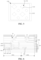
- FIG. 3 is a partial schematic structural top view of the first openings and the second openings of the display panel in FIG. 2
- FIG. 4 is a second schematic cross-sectional structural diagram of the display panel according to an embodiment of the present disclosure
- FIG. 5 is a partial schematic structural top view of the first openings and the second openings of the display panel in FIG. 4 .
- an orthographic projection of the second openings V2 on the substrate 101 covers an orthographic projection of the first openings V1 on the substrate 101.
- the shielding layer 112 can shield a part of lower metal wirings.
- the orthographic projection of the shielding layer 112 on the substrate 101 does not overlap the orthographic projection of the light-emitting layer 113 on the substrate 101, so in this embodiment, the visible mura phenomenon can be significantly improved without affecting a light-emitting effect of the light-emitting layer 113.
- a shape of the orthographic projection of the second openings V2 on the substrate 101 is same as that of the orthographic projection of corresponding first openings V1 on the substrate 101. That is, the shape of the orthographic projection of the second openings V2 on the substrate 101 is same as that of the orthographic projection of corresponding light-emitting layer 113 on the substrate 101.
- Each pixel unit 115 being arranged in a pearl type arrangement is taken as an example for description.
- Each pixel unit 115 includes two red light-emitting pixels, two blue light-emitting pixels, and four green light-emitting pixels.
- Shapes of the red light-emitting pixels and the blue light-emitting pixels are octagonal, and a shape of the green light-emitting pixels is oval. Then, in this embodiment, the shape of the orthographic projection of the second openings V2 on the substrate 101 is octagonal or oval.
- the pixel unit 115 may use other arrangement method.
- the shape of the orthographic projection of the light-emitting layer 113 on the substrate 101 may also be rectangular, circular, or other polygonal.
- the shape of the second openings V2 may also be different from the shape of the first openings V1, which is not limited in the present disclosure, and the second openings V2 may be designed according to an arrangement method and the shape of the first openings V1.
- a ratio of an orthographic projection area of the second openings V2 on the substrate 101 to an orthographic projection area of the first openings V1 on the substrate 101 ranges from 1 to 1.5.
- This embodiment includes two situations.
- the first situation is that referring to FIGs. 2 and 3 , a gap is between an edge of the orthographic projection of the second openings V2 on the substrate 101 and an edge of the orthographic projection of the first openings V1 on the substrate 101. That is, the orthographic projection area of the second openings V2 on the substrate 101 is greater than the orthographic projection area of the first openings V1 on the substrate 101. That is, the ratio of the orthographic projection area of the second openings V2 on the substrate 101 to the orthographic projection area of the first openings V1 on the substrate 101 is greater than 1 and is less than or equal to 1.5.
- the second situation is that referring to FIGs. 4 and 5 , a difference between FIGs. 4 and 2 and between FIGs. 5 and 3 is that the edge of the orthographic projection of the second openings V2 on the substrate 101 completely overlaps the edge of the orthographic projection of the first openings V1 on the substrate 101. That is, the orthographic projection area of the second openings V2 on the substrate 101 is equal to the orthographic projection area of the first openings V1 on the substrate 101. That is, the ratio of the orthographic projection area of the second openings V2 on the substrate 101 to the orthographic projection area of the first openings V1 on the substrate 101 is equal to 1. It can be understood that compared to the first situation, an area of the lower metal wirings shielded by the shielding layer 112 in the second situation is larger, thereby better improving the visible mura.
- FIG. 6 is a third schematic cross-sectional structural diagram of the display panel according to an embodiment of the present disclosure
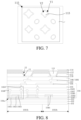
- FIG. 7 is a partial schematic structural top view of the first openings and the second openings of the display panel in FIG. 6 .
- a difference between FIGs. 6 and 2 and between FIGs. 7 and 3 is that the orthographic projection of the first openings V1 on the substrate 101 covers the orthographic projection of the second openings V2 on the substrate 101.
- the shielding layer 112 can shield almost all the lower metal wirings.
- this embodiment can further improve the visible mura but sacrifices the light-emitting effect of the light-emitting layer 113.
- the ratio of the orthographic projection area of the second openings V2 on the substrate 101 to the orthographic projection area of the first openings V1 on the substrate 101 ranges from 0.8 to 1.
- the orthographic projection area of the second openings V2 on the substrate 101 cannot be too small, or the light-emitting effect of the light-emitting layer 113 in the fan-out display area 100b will be greatly reduced, thereby causing display effects between the fan-out display area 100b and the normal display area 100a to have an overly large difference, reducing display uniformity.
- FIG. 8 is a fourth schematic cross-sectional structural diagram of the display panel according to an embodiment of the present disclosure
- FIG. 9 is a partial schematic structural top view of the first openings and the second openings of the display panel in FIG. 8 .
- a difference between FIGs. 8 and 6 and between FIGs. 9 and 7 is that in order to improve the disadvantage that the light-emitting effect of the light-emitting layer 113 is reduced, the light-emitting layer 113 covers a side wall and a bottom of the second openings V2. That is, the shielding layer 112 play a role of the pixel definition layer 111, and the second openings V2 are equivalent to the pixel openings.
- the light-emitting layer 113 completely covers the side wall and the bottom of the second openings V2. Since a height of the shielding layer 112 is higher than a height of the pixel definition layer 111, that is, a height of the second openings V2 is higher than a height of the first openings V1, this embodiment can increase the effective light-emitting area of the light-emitting layer 113 by disposing the light-emitting layer 113 in the second openings V2. Therefore, it is beneficial to improve the light-emitting effect of the light-emitting layer 113, thereby realizing the objective of improving the visible mura without affecting the light-emitting effect of the light-emitting layer 113.
- FIG. 10 is a fifth schematic cross-sectional structural diagram of the display panel according to an embodiment of the present disclosure.
- the pixel definition layer 111 and the shielding layer 112 use a same light shielding material.
- a material of the pixel definition layer 111 is also the black matrix. It can be understood that the pixel definition layer 111 not only plays a role of limiting the light-emitting layer 113, but also plays a same role as the shielding layer 112. Therefore, the pixel definition layer 111 can shield most of the pixel driving circuit units 104a, the fan-out wirings 104b, and the connecting wirings 1081, thereby further improving the visible mura.
- the thickness of the shielding layer 112 may be set thinner, and even the technical problem of the present disclosure can be solved without setting the shielding layer 112, thereby being beneficial to realize thinning and lightening of the display panel.
- the display panel further includes a cathode 114, and the shielding layer 112 is disposed between the cathode 114 and the pixel definition layer 111.
- the cathode 114 covers the pixel definition layer 111, the shielding layer 112, and the light-emitting layer 113.
- the cathode 114 covers the shielding layer 112 and the light-emitting layer 113.
- the display panel further includes an electron injection layer, an electron transport layer, a hole transport layer, and a hole injection layer disposed in sequence along the direction away from the substrate 101.
- the electron injection layer, the electron transport layer, the hole transport layer, and the hole injection layer are disposed in the first openings V1.
- the electron injection layer and the electron transport layer are disposed between the light-emitting layer 113 and the anodes 110.
- the hole transport layer and the hole injection layer are disposed between the light-emitting layer 113 and the cathode 114.
- the display panel further includes an encapsulation layer covering one side of the cathode 114 away from the substrate 101, and the encapsulation layer is configured to encapsulate the light-emitting layer 113 to prevent external water vapor and oxygen from intruding and damaging the light-emitting layer 113.
- the encapsulation layer may be formed using thin film encapsulation, and the encapsulation layer may be a single-layer or multi-layer encapsulation stacked structure.
- the encapsulation layer adopts an inorganic/organic/inorganic multi-layer encapsulation stacked structure, which is beneficial to improve an encapsulation effect.
- the display panel further includes a touch layer disposed on one side of the encapsulation layer away from the substrate 101, and a touch control type of the touch layer may be a self-capacitive type or a mutual capacitive type.
- the touch control type of the touch layer may be selected according to actual situations, and is not limited in the present disclosure.
- the display panel further includes a polarizer and a coverplate stacked in sequence on one side of the touch layer away from the substrate 101.
- the polarizer is attached to a surface of the touch layer away from the substrate 101 by an optical adhesive
- the coverplate is attached to a surface of the polarizer away from the substrate 101 by the optical adhesive.
- An embodiment of the present disclosure further provides a display device, which includes the display panel in the above embodiments.
- the display device includes fixed terminals such as televisions and desktop computers, mobile terminals such as mobile phones and notebook computers, and wearable devices such as wristbands, virtual display (VR) devices, and augmented display (AR) devices.
- fixed terminals such as televisions and desktop computers
- mobile terminals such as mobile phones and notebook computers
- wearable devices such as wristbands, virtual display (VR) devices, and augmented display (AR) devices.
- VR virtual display
- AR augmented display
- An embodiment of the present disclosure further provides a manufacturing method of the display panel.
- the display panel includes the normal display area 100a and the fan-out display area 100b disposed on one side of the normal display area 100a.
- the fan-out display area 100b includes the first area 1001b and the second area 1002b arranged in sequence in the direction from the normal display area 100a toward the fan-out display area 100b.
- the manufacturing method includes following steps.
- the beneficial effect is that in the display panel and the display device provided in the embodiments of the present disclosure, by disposing the shielding layer on one side of the pixel definition layer away from the substrate and allowing the second openings of the shielding layer to correspond to the first openings of the pixel definition layer, the shielding layer can be used to block light reflected by the metal wirings. Therefore, the light reflected by the metal wirings in the fan-out display area and the normal display area are more uniform, thereby being beneficial to improve the visible mura phenomenon in the fan-out display area and the normal display area caused by the densities of the metal wirings in the fan-out display area and the normal display area being different when screens are turned off and turned on.
Landscapes
- Engineering & Computer Science (AREA)
- Microelectronics & Electronic Packaging (AREA)
- Physics & Mathematics (AREA)
- Optics & Photonics (AREA)
- Electroluminescent Light Sources (AREA)
- Devices For Indicating Variable Information By Combining Individual Elements (AREA)
Abstract
A display panel and a display device are disclosed. The display panel includes a normal display area and a fan-out display area, and the fan-out display area includes a first area and a second area. Pixel driving circuit units of the display panel are located in the normal display area and the first area, and fan-out wirings are located in the second area. A shielding layer is disposed on one side of a pixel definition layer away from a substrate, and second openings of the shielding layer are defined corresponding to first openings of the pixel definition layer, thereby being beneficial to improve visible mura.
Description
- The present disclosure relates to the field of display technologies, and more particularly, to a display panel and a display device.
- With development of organic light-emitting diode (OLED) panel technologies, narrow bezel techniques have become a differentiated technique that attracts user groups. Fan-out in AA (FIAA) technique, that is, fan-out wirings in display areas, is used as a new layout method, which can effectively reduce lower bezels of panels. In the FIAA technique, a design of introducing multiple layers of connecting wirings is used to squeeze out wiring space for fan-out wirings. However, during wiring processes of the connecting wirings, limitation of wiring space easily causes densities of metal wirings in fan-out display areas and normal display areas to be different. Different densities easily cause light reflected from metal wirings to be uneven, thereby causing a visible uneven display (mura) phenomenon in the fan-out display areas and the normal display areas when screens are turned off and turned on.
- Technical problem: an embodiment of the present disclosure provides a display panel and a display device to solve a technical problem of a visible display mura phenomenon in the fan-out display areas and the normal display areas caused by the densities of the metal wirings in the fan-out display areas and the normal display areas being different in current display panels and display devices.
- In order to solve the above problem, the present disclosure provides technical solutions as follows.
- The present disclosure provides a display panel, which includes a normal display area and a fan-out display area disposed on one side of the normal display area, wherein, the fan-out display area includes a first area and a second area arranged in sequence in a direction from the normal display area toward the fan-out display area, and the display panel includes:
- a substrate;
- a driving circuit layer disposed on one side of the substrate and including a plurality of pixel driving circuit units and a plurality of fan-out wirings, wherein, the pixel driving circuit units are disposed in the normal display area and the first area, the fan-out wirings are disposed in the second area, and a density of the pixel driving circuit units disposed in the first area is greater than a density of the pixel driving circuit units disposed in the normal display area;
- at least one connecting wiring layer disposed on one side of the driving circuit layer away from the substrate, wherein, each connecting wiring layer includes a plurality of connecting wirings;
- a plurality of anodes disposed on one side of the at least one connecting wiring layer away from the substrate, wherein, the pixel driving circuit units are electrically connected to corresponding anodes by the connecting wirings;
- a pixel definition layer disposed on one side of the at least one connecting wiring layer away from the substrate and including a plurality of first openings exposing at least a part of the anodes; and
- a light-emitting layer disposed in the first openings;
- wherein, the display panel further includes a shielding layer, the pixel definition layer and the shielding layer use a same light-shielding material, and the shielding layer is disposed on one side of the pixel definition layer away from the substrate and includes a plurality of second openings defined corresponding to the first openings.
- Based on the display panel provided in the present disclosure, an orthographic projection of the second openings on the substrate covers an orthographic projection of the first openings on the substrate.
- Based on the display panel provided in the present disclosure, a ratio of an orthographic projection area of the second openings on the substrate to an orthographic projection area of the first openings on the substrate ranges from 1 to 1.5.
- Based on the display panel provided in the present disclosure, an orthographic projection of the first openings on the substrate covers an orthographic projection of the second openings on the substrate.
- Based on the display panel provided in the present disclosure, a ratio of an orthographic projection area of the second openings on the substrate to an orthographic projection area of the first openings on the substrate ranges from 0.8 to 1.
- Based on the display panel provided in the present disclosure, the light-emitting layer covers a side wall and a bottom of the second openings.
- Based on the display panel provided in the present disclosure, a thickness of the shielding layer in a direction perpendicular to the substrate ranges from 1 µm to 1.5 µm.
- Based on the display panel provided in the present disclosure, a material of the shielding layer includes a black matrix.
- Based on the display panel provided in the present disclosure, the shielding layer is disposed between the cathode and the pixel definition layer.
- The present disclosure provides a display panel, which includes a normal display area and a fan-out display area disposed on one side of the normal display area, wherein, the fan-out display area includes a first area and a second area arranged in sequence in a direction from the normal display area toward the fan-out display area, and the display panel includes:
- a substrate;
- a driving circuit layer disposed on one side of the substrate and including a plurality of pixel driving circuit units and a plurality of fan-out wirings, wherein, the pixel driving circuit units are disposed in the normal display area and the first area, the fan-out wirings are disposed in the second area, and a density of the pixel driving circuit units disposed in the first area is greater than a density of the pixel driving circuit units disposed in the normal display area;
- at least one connecting wiring layer disposed on one side of the driving circuit layer away from the substrate, wherein, each connecting wiring layer includes a plurality of connecting wirings;
- a plurality of anodes disposed on one side of the at least one connecting wiring layer away from the substrate, wherein, the pixel driving circuit units are electrically connected to corresponding anodes by the connecting wirings;
- a pixel definition layer disposed on one side of the at least one connecting wiring layer away from the substrate and including a plurality of first openings exposing at least a part of the anodes; and
- a light-emitting layer disposed in the first openings;
- wherein, the display panel further includes a shielding layer disposed on one side of the pixel definition layer away from the substrate and including a plurality of second openings defined corresponding to the first openings.
- Based on the display panel provided in the present disclosure, an orthographic projection of the second openings on the substrate covers an orthographic projection of the first openings on the substrate.
- Based on the display panel provided in the present disclosure, a ratio of an orthographic projection area of the second openings on the substrate to an orthographic projection area of the first openings on the substrate ranges from 1 to 1.5.
- Based on the display panel provided in the present disclosure, an orthographic projection of the first openings on the substrate covers an orthographic projection of the second openings on the substrate. Based on the display panel provided in the present disclosure, an orthographic projection of the first openings on the substrate covers an orthographic projection of the second openings on the substrate.
- Based on the display panel provided in the present disclosure, a ratio of an orthographic projection area of the second openings on the substrate to an orthographic projection area of the first openings on the substrate ranges from 0.8 to 1.
- Based on the display panel provided in the present disclosure, the light-emitting layer covers a side wall and a bottom of the second openings.
- Based on the display panel provided in the present disclosure, a thickness of the shielding layer in a direction perpendicular to the substrate ranges from 1 µm to 1.5 µm.
- Based on the display panel provided in the present disclosure, a material of the shielding layer includes a black matrix.
- Based on the display panel provided in the present disclosure, the shielding layer is disposed between the cathode and the pixel definition layer.
- Based on the display panel provided in the present disclosure, the at least one connecting wiring layer includes a first connecting wiring layer and a second connecting wiring layer, and the display panel further includes a first planarization layer, a second planarization layer, and a third planarization layer stacked in sequence in a direction away from the substrate;
- the first planarization layer covers the side of the driving circuit layer away from the substrate, the first connecting wiring layer is disposed between the first planarization layer and the second planarization layer, and the second connecting wiring layer is disposed between the second planarization layer and the third planarization layer; and
- the driving circuit layer is electrically connected to the connecting wirings in the first connecting wiring layer by through-holes penetrating the first planarization layer, the first connecting wiring layer is electrically connected to the connecting wirings in the second connecting wiring layer by through-holes penetrating the second planarization layer, and the second connecting wiring layer is electrically connected to the anodes by through-holes penetrating the third planarization layer.
- An embodiment of the present disclosure further provides a display device, which includes a display panel including a normal display area and a fan-out display area disposed on one side of the normal display area, wherein, the fan-out display area includes a first area and a second area arranged in sequence in a direction from the normal display area toward the fan-out display area, and the display panel includes:
- a substrate;
- a driving circuit layer disposed on one side of the substrate and including a plurality of pixel driving circuit units and a plurality of fan-out wirings, wherein, the pixel driving circuit units are disposed in the normal display area and the first area, the fan-out wirings are disposed in the second area, and a density of the pixel driving circuit units disposed in the first area is greater than a density of the pixel driving circuit units disposed in the normal display area;
- at least one connecting wiring layer disposed on one side of the driving circuit layer away from the substrate, wherein, each connecting wiring layer includes a plurality of connecting wirings;
- a plurality of anodes disposed on one side of the at least one connecting wiring layer away from the substrate, wherein, the pixel driving circuit units are electrically connected to corresponding anodes by the connecting wirings;
- a pixel definition layer disposed on one side of the at least one connecting wiring layer away from the substrate and including a plurality of first openings exposing at least a part of the anodes; and
- a light-emitting layer disposed in the first openings;
- wherein, the display panel further includes a shielding layer disposed on one side of the pixel definition layer away from the substrate and including a plurality of second openings defined corresponding to the first openings.
- Beneficial effect: the beneficial effect of the present disclosure is that in the display panel and the display device provided in the present disclosure, by disposing the shielding layer on one side of the pixel definition layer away from the substrate and allowing the second openings of the shielding layer to correspond to the first openings of the pixel definition layer, the shielding layer can be used to block light reflected by metal wirings. Therefore, the light reflected by the metal wirings in the fan-out display area and the normal display area are more uniform, thereby being beneficial to improve a visible mura phenomenon in the fan-out display area and the normal display area caused by densities of the metal wirings in the fan-out display area and the normal display area being different when screens are turned off and turned on.
- The accompanying figures to be used in the description of embodiments of the present disclosure or prior art will be described in brief to more clearly illustrate the technical solutions of the embodiments or the prior art. The accompanying figures described below are only part of the embodiments of the present disclosure, from which figures those skilled in the art can derive further figures without making any inventive efforts.
-
FIG. 1 is a schematic planar diagram of a display panel according to an embodiment of the present disclosure. -
FIG. 2 is a first schematic cross-sectional structural diagram of the display panel along line A-A inFIG. 1 . -
FIG. 3 is a partial schematic structural top view of first openings and second openings of the display panel inFIG. 2 according to an embodiment of the present disclosure. -
FIG. 4 is a second schematic cross-sectional structural diagram of the display panel along line A-A inFIG. 1 . -
FIG. 5 is a partial schematic structural top view of the first openings and the second openings of the display panel inFIG. 4 according to an embodiment of the present disclosure. -
FIG. 6 is a third schematic cross-sectional structural diagram of the display panel along line A-A inFIG. 1 . -
FIG. 7 is a partial schematic structural top view of the first openings and the second openings of the display panel inFIG. 6 according to an embodiment of the present disclosure. -
FIG. 8 is a fourth schematic cross-sectional structural diagram of the display panel along line A-A inFIG. 1 . -
FIG. 9 is a partial schematic structural top view of the first openings and the second openings of the display panel inFIG. 8 according to an embodiment of the present disclosure. -
FIG. 10 is a fifth schematic cross-sectional structural diagram of the display panel along line A-A inFIG. 1 . - Elements in the drawings are designated by reference numerals listed below.
- 100a: normal display area; 100b: fan-out display area; 1001b: first area; 1002b: second area;
- 101: substrate; 102: barrier layer; 103: buffer layer; 104: driving circuit layer; 105: first planarization layer; 106: first connecting wiring layer; 107: second planarization layer; 108: second connecting wiring layer; 1081: connecting wiring; 109: third planarization layer; 110: anode; 111: pixel definition layer; 112: shielding layer; 113: light-emitting layer; 114: cathode; 115: pixel unit;
- 104a: pixel driving circuit units; 104b: fan-out wirings; 1041: active layer; 1042: first gate insulating layer; 1043: first gate electrode layer; 1044: second gate insulating layer; 1045: second gate electrode layer; 1046: first interlayer dielectric layer; 1047: second interlayer dielectric layer; 1048: first source and drain electrode metal layer; 1049: fourth planarization layer; 1050: second source and drain electrode metal layer;
- V1: first opening; and V2: second opening.
- The technical solutions in the embodiments of the present disclosure will be clearly and completely described below with reference to the drawings in the embodiments of the present disclosure. Obviously, the described embodiments are only a part of the embodiments of the present disclosure, but not all the embodiments. Based on the embodiments in the present disclosure, all other embodiments obtained by those skilled in the art without creative efforts are within the scope of the present disclosure. In addition, it should be understood that the specific embodiments described herein are only used to illustrate and explain the disclosure and are not used to limit the disclosure. In the present disclosure, in the case of no explanation to the contrary, the orientation words used such as "on" and "under" usually refer to upper and lower directions of the device in actual use or working state, and specifically the directions in the drawings; and "inside" and "outside" refers to the outline of the device.
- Referring to
FIGs. 1 and 2, FIG. 1 is a schematic planar diagram of a display panel according to an embodiment of the present disclosure, andFIG. 2 is a first schematic cross-sectional structural diagram of the display panel according to an embodiment of the present disclosure. The display panel provided in this embodiment includes anormal display area 100a and a fan-outdisplay area 100b disposed on one side of thenormal display area 100a. The fan-outdisplay area 100b includes afirst area 1001b and asecond area 1002b arranged in sequence in a direction from thenormal display area 100a toward the fan-outdisplay area 100b. The display panel includes asubstrate 101, a drivingcircuit layer 104, a connecting wiring layer, a plurality ofanodes 110, apixel definition layer 111, and a light-emittinglayer 113. - The fan-out
display area 100b is disposed adjacent to thenormal display area 100a, and the fan-outdisplay area 100b may be disposed on an edge of the display panel. Further, in this embodiment, the fan-outdisplay area 100b is disposed on a lower edge of the display panel. - The driving
circuit layer 104 is disposed on one side of thesubstrate 101 and includes a plurality of pixel drivingcircuit units 104a and a plurality of fan-outwirings 104b. The pixeldriving circuit units 104a are disposed in thenormal display area 100a and thefirst area 1001b, and the fan-outwirings 104b are disposed in thesecond area 1002b. At least one connecting wiring layer is disposed on one side of the drivingcircuit layer 104 away from thesubstrate 101, and each connecting wiring layer includes a plurality of connecting wirings 1081. The plurality ofanodes 110 are disposed on one side of a top layer of the at least one connecting wiring layer away from thesubstrate 101, and the pixel drivingcircuit units 104a are electrically connected to correspondinganodes 110 by the connecting wirings 1081. Thepixel definition layer 111 is disposed on one side of the at least one connecting wiring layer away from thesubstrate 101 and includes a plurality of first openings V1 exposing at least a part of theanodes 110. The light-emittinglayer 113 is disposed in the first openings V1. - Wherein, the display panel further includes a
shielding layer 112 disposed on one side of thepixel definition layer 111 away from thesubstrate 101, and theshielding layer 112 includes a plurality of second openings V2 defined corresponding to the first openings V1. - It can be understood that in current technology, each two adjacent light-emitting pixels in display areas of display panels have a same spacing between each other. That is, pixel densities in the display areas are same everywhere. Since each light-emitting pixel is electrically connected to a corresponding pixel driving
circuit unit 104a, in current technology, densities of the pixel drivingcircuit units 104a in the display areas of the display panels are same everywhere, and each two adjacent pixel drivingcircuit units 104a have a same spacing between each other. - The display panel of the present disclosure includes the
normal display area 100a and the fan-outdisplay area 100b. A position of each light-emitting pixel and a spacing between two adjacent light-emitting pixels in the fan-outdisplay area 100b are consistent with those in thenormal display area 100a. That is, a pixel density of the fan-outdisplay area 100b is same as a pixel density of thenormal display area 100a. However, a difference between the present disclosure and current technology is that in the present disclosure, the pixel drivingcircuit units 104a in the fan-outdisplay area 100b are electrically connected to correspondinganodes 110 by the connecting wirings 1081 to drive corresponding light-emitting pixels in the fan-outdisplay area 100b to emit light. The disposition of the connecting wiring layer can allow all pixel drivingcircuit units 104a in the fan-outdisplay area 100b to be concentrated in thefirst area 1001b of the fan-outdisplay area 100b without changing original positions of the light-emitting pixels in the fan-outdisplay area 100b, and allow thesecond area 1002b to be not provided with any of the pixel drivingcircuit units 104a. Therefore, thesecond area 1002b can be used to dispose the fan-outwirings 104b. Compared to the fan-outwirings 104b being disposed in a non-display area of the display panels in current technology, since the fan-outwirings 104b of the present disclosure can be disposed in the display area, an area of the display area is increased, and an area of the non-display area is reduced, thereby being beneficial to further realizing narrow bezels and full-screen technology. - Specifically, by reducing the spacing between every two adjacent pixel driving
circuit units 104a in the fan-outdisplay area 100b or reducing a size of the pixel drivingcircuit units 104a in the fan-outdisplay area 100b, an overall space occupied by all the pixel drivingcircuit units 104a located in the fan-outdisplay area 100b can be reduced, and a partial space of the drivingcircuit layer 104 in the fan-outdisplay area 100b can be squeezed out for disposing the fan-outwirings 104b. Of course, other methods may also be used, and it is not limited in the present disclosure. - As can be seen from the above, in the present disclosure, since the pixel driving
circuit units 104a in the fan-outdisplay area 100b are all concentrated in thefirst area 1001b of the fan-outdisplay area 100b, a density of the pixel drivingcircuit units 104a located in thefirst area 1001b is greater than a density of the pixel drivingcircuit units 104a located in thenormal display area 100a. Since the pixel drivingcircuit units 104a include a plurality of metal wirings, a density of the metal wirings in thefirst area 1001b is greater than a density of the metal wirings in thenormal display area 100a. - Further, first, the fan-out
wirings 104b are disposed in thesecond area 1002b of the fan-outdisplay area 100b, and the fan-outwirings 104b are metal wirings newly introduced into the fan-outdisplay area 100b; and second, due to limitation of arrangement space, a density of the connecting wirings 1081 in the fan-outdisplay area 100b is greater than a density of the connecting wirings 1081 in thenormal display area 100a, and the connecting wirings 1081 are transparent metal wirings. Therefore, in the present disclosure, the density of the metal wirings in the fan-outdisplay area 100b is greater than the density of the metal wirings in thenormal display area 100a, and a density difference between the metal wirings easily causes a visible mura phenomenon in the fan-outdisplay area 100b and thenormal display area 100a. - Based on this, in the present disclosure, by disposing the
shielding layer 112 on one side of thepixel definition layer 111 away from thesubstrate 101 and allowing the second openings V2 of theshielding layer 112 to correspond to the first openings V1 of thepixel definition layer 111, theshielding layer 112 can be used to block light reflected by the metal wirings. Therefore, the light reflected by the metal wirings in the fan-outdisplay area 100b and thenormal display area 100a are more uniform, thereby being beneficial to improve the visible mura phenomenon in the fan-outdisplay area 100b and thenormal display area 100a caused by the densities of the metal wirings in the fan-outdisplay area 100b and thenormal display area 100a being different when screens are turned off and turned on. - In the embodiments of the present disclosure, a display area of the display panel is composed of the
normal display area 100a and the fan-outdisplay area 100b, so both thenormal display area 100a and the fan-outdisplay area 100b have display function, and the fan-outwirings 104b are disposed in the fan-outdisplay area 100b. The display panel further includes a non-display area (not shown in the figure), and the fan-outdisplay area 100b is disposed on one side of thenormal display area 100a. Specifically, the fan-outdisplay area 100b is disposed between thenormal display area 100a and the non-display area. - Further, the display panel further includes a driver chip, and the driver chip may also be disposed in the fan-out
display area 100b. In this case, the non-display area may be omitted, so the display panel can realize frameless and full screen. - In this embodiment, the
substrate 101 is a flexible substrate, and the flexible substrate is generally an organic polymer material, such as polyimide and polyethylene terephthalate. - In this embodiment, between the
substrate 101 and the drivingcircuit layer 104, abarrier layer 102 and abuffer layer 103 are further stacked in sequence along a direction away from thesubstrate 101. Thebarrier layer 102 is used to block water and oxygen to prevent external water vapor or oxygen from eroding the display panel. A material of thebarrier layer 102 includes one or more of silicon oxide, silicon nitride, silicon oxynitride, or amorphous silicon. Thebuffer layer 103 mainly plays a role of buffering and protection, and a material of thebuffer layer 103 includes one or both of silicon nitride and silicon oxide. - The pixel
driving circuit units 104a include a plurality of thin film transistors. In this embodiment of the present disclosure, the thin film transistors may be thin film transistors with a double gate structure. Specifically, the thin film transistors include anactive layer 1041, a firstgate insulating layer 1042, a firstgate electrode layer 1043, a secondgate insulating layer 1044, a secondgate electrode layer 1045, a firstinterlayer dielectric layer 1046, a secondinterlayer dielectric layer 1047, and a first source and drainelectrode metal layer 1048 disposed in sequence along the direction away from thesubstrate 101. Wherein, the first source and drainelectrode metal layer 1048 is electrically connected to theactive layer 1041 by through-holes penetrating through the secondinterlayer dielectric layer 1047, the firstinterlayer dielectric layer 1046, the secondgate insulating layer 1044, and the firstgate insulating layer 1042. Of course, in some embodiments, the thin film transistors may also be thin film transistors having only one gate electrode layer. In addition, the thin film transistors may also be top gate or bottom gate structures, which is not limited in the present disclosure. - In this embodiment, the
anodes 110 may use a stacked structure of indium tin oxide (ITO)/silver (Ag)/ITO. ITO has good water blocking properties, which can prevent water vapor or oxygen from diffusing to the light-emittinglayer 113 through theanodes 110. Therefore, black spots on the display panel caused by the light-emittinglayer 113 being corroded by water vapor or oxygen can be prevented, thereby improving display effect of the display panel. - It should be noted that the
pixel definition layer 111 defines the plurality of first openings V1, and the first openings V1 are pixel openings. In the embodiments of the present disclosure, the first openings V1 refer to effective light-emitting pixel openings, and an orthographic projection area of the first openings V1 on thesubstrate 101 is an orthographic projection area of the light-emittinglayer 113 on thesubstrate 101. - In this embodiment, the at least one connecting wiring layer includes two connecting wiring layers, and specifically includes a first connecting
wiring layer 106 and a second connecting wiring layer 108. The display panel further includes afirst planarization layer 105, asecond planarization layer 107, and athird planarization layer 109 stacked in sequence along the direction away from thesubstrate 101. Thefirst planarization layer 105 covers the side of the drivingcircuit layer 104 away from thesubstrate 101, the first connectingwiring layer 106 is disposed between thefirst planarization layer 105 and thesecond planarization layer 107, and the second connecting wiring layer 108 is disposed between thesecond planarization layer 107 and thethird planarization layer 109. The drivingcircuit layer 104 is electrically connected to the connecting wirings 1081 in the first connectingwiring layer 106 by through-holes penetrating thefirst planarization layer 105, the first connectingwiring layer 106 is electrically connected to the connecting wirings 1081 in the second connecting wiring layer 108 by through-holes penetrating thesecond planarization layer 107, and the second connecting wiring layer 108 is electrically connected to correspondinganodes 110 by through-holes penetrating thethird planarization layer 109. - Specifically, the connecting wiring layers are transparent conductive layers, and the connecting wirings 1081 are transparent wirings. A material of the connecting wirings 1081 is a transparent conductive material, and the transparent conductive material includes any one of indium tin oxide, indium oxide, indium zinc oxide, or silver nanowires.
- Of course, in other embodiments, the at least one connecting wiring layer may also have three layers, four layers, five layers,... or even more layers, which is not limited in the present disclosure. Correspondingly, the display panel also needs to dispose a corresponding number of planarization layers for disposing between two adjacent connecting wiring layers. Specifically, a material of the planarization layers includes transparent organic materials, and the transparent organic materials include polyimide and photoresist materials.
- Further, the thin film transistors may also be designed with double source and drain electrode metal layers to reduce impedance. Specifically, the thin film transistors also include a second source and drain
electrode metal layer 1050 and afourth planarization layer 1049. Thefourth planarization layer 1049 covers one side of the first source and drainelectrode metal layer 1048 away from thesubstrate 101, the second source and drainelectrode metal layer 1050 is disposed on one side of thefourth planarization layer 1049 away from thesubstrate 101, and thefirst planarization layer 105 covers one side of the second source and drainelectrode metal layer 1050 away from thesubstrate 101. The first source and drainelectrode metal layer 1048 is electrically connected to the second source and drain electrodemetal electrode layer 1050 by through-holes penetrating thefourth planarization layer 1049, and the second source and drainelectrode metal layer 1050 is electrically connected to the connecting wirings 1081 in the first connectingwiring layer 106 by through-holes penetrating thefirst planarization layer 105. - In this embodiment, the fan-out
wirings 104b are disposed in a same layer as the firstgate electrode layer 1043 or the secondgate electrode layer 1045, and are prepared in a same process step as the firstgate electrode layer 1043 or the secondgate electrode layer 1045. - In the embodiment, a thickness of the
shielding layer 112 in a direction perpendicular to thesubstrate 101 ranges from 1 µm to 1.5 µm. The thickness of theshielding layer 112 should not be too large or too small. If the thickness is too large, the overall thickness of the display panel will increase, which is contrary to the current trend of thinner and lighter displays. If the thickness is too small, the light shielding effect will be poor and is not beneficial to improve the visible mura phenomenon. - Optionally, the thickness of the
shielding layer 112 in the direction perpendicular to thesubstrate 101 may be 1 µm, 1.1 µm, 1.2 µm, 1.3 µm, 1.4 µm, or 1.5 µm. In this embodiment, the thickness of theshielding layer 112 in the direction perpendicular to thesubstrate 101 is 1.2 µm. - In the embodiments of the present disclosure, a material of the
shielding layer 112 includes a black matrix. Of course, in some embodiments, the material of theshielding layer 112 may be other light shielding materials, which is not limited in the present disclosure. - In the embodiments of the present disclosure, the
shielding layer 112 may be formed by plasma enhanced chemical vapor deposition (PECVD). In other embodiments, theshielding layer 112 may also be formed by chemical vapor deposition or atomic layer deposition. - In an embodiment of the present disclosure, referring to
FIGs. 2 to 5 ,FIG. 3 is a partial schematic structural top view of the first openings and the second openings of the display panel inFIG. 2 ,FIG. 4 is a second schematic cross-sectional structural diagram of the display panel according to an embodiment of the present disclosure, andFIG. 5 is a partial schematic structural top view of the first openings and the second openings of the display panel inFIG. 4 . - In this embodiment, an orthographic projection of the second openings V2 on the
substrate 101 covers an orthographic projection of the first openings V1 on thesubstrate 101. In this embodiment, theshielding layer 112 can shield a part of lower metal wirings. The orthographic projection of theshielding layer 112 on thesubstrate 101 does not overlap the orthographic projection of the light-emittinglayer 113 on thesubstrate 101, so in this embodiment, the visible mura phenomenon can be significantly improved without affecting a light-emitting effect of the light-emittinglayer 113. - In the embodiments, a shape of the orthographic projection of the second openings V2 on the
substrate 101 is same as that of the orthographic projection of corresponding first openings V1 on thesubstrate 101. That is, the shape of the orthographic projection of the second openings V2 on thesubstrate 101 is same as that of the orthographic projection of corresponding light-emittinglayer 113 on thesubstrate 101. Eachpixel unit 115 being arranged in a pearl type arrangement is taken as an example for description. Eachpixel unit 115 includes two red light-emitting pixels, two blue light-emitting pixels, and four green light-emitting pixels. Shapes of the red light-emitting pixels and the blue light-emitting pixels are octagonal, and a shape of the green light-emitting pixels is oval. Then, in this embodiment, the shape of the orthographic projection of the second openings V2 on thesubstrate 101 is octagonal or oval. - Of course, in other embodiments, the
pixel unit 115 may use other arrangement method. The shape of the orthographic projection of the light-emittinglayer 113 on thesubstrate 101 may also be rectangular, circular, or other polygonal. The shape of the second openings V2 may also be different from the shape of the first openings V1, which is not limited in the present disclosure, and the second openings V2 may be designed according to an arrangement method and the shape of the first openings V1. - Specifically, a ratio of an orthographic projection area of the second openings V2 on the
substrate 101 to an orthographic projection area of the first openings V1 on thesubstrate 101 ranges from 1 to 1.5. - This embodiment includes two situations. The first situation is that referring to
FIGs. 2 and3 , a gap is between an edge of the orthographic projection of the second openings V2 on thesubstrate 101 and an edge of the orthographic projection of the first openings V1 on thesubstrate 101. That is, the orthographic projection area of the second openings V2 on thesubstrate 101 is greater than the orthographic projection area of the first openings V1 on thesubstrate 101. That is, the ratio of the orthographic projection area of the second openings V2 on thesubstrate 101 to the orthographic projection area of the first openings V1 on thesubstrate 101 is greater than 1 and is less than or equal to 1.5. - The second situation is that referring to
FIGs. 4 and5 , a difference betweenFIGs. 4 and2 and betweenFIGs. 5 and3 is that the edge of the orthographic projection of the second openings V2 on thesubstrate 101 completely overlaps the edge of the orthographic projection of the first openings V1 on thesubstrate 101. That is, the orthographic projection area of the second openings V2 on thesubstrate 101 is equal to the orthographic projection area of the first openings V1 on thesubstrate 101. That is, the ratio of the orthographic projection area of the second openings V2 on thesubstrate 101 to the orthographic projection area of the first openings V1 on thesubstrate 101 is equal to 1. It can be understood that compared to the first situation, an area of the lower metal wirings shielded by theshielding layer 112 in the second situation is larger, thereby better improving the visible mura. - In an embodiment of the present disclosure, referring to
FIGs. 6 and7 ,FIG. 6 is a third schematic cross-sectional structural diagram of the display panel according to an embodiment of the present disclosure, andFIG. 7 is a partial schematic structural top view of the first openings and the second openings of the display panel inFIG. 6 . A difference betweenFIGs. 6 and2 and betweenFIGs. 7 and3 is that the orthographic projection of the first openings V1 on thesubstrate 101 covers the orthographic projection of the second openings V2 on thesubstrate 101. In this embodiment, theshielding layer 112 can shield almost all the lower metal wirings. Since the orthographic projection of theshielding layer 112 on thesubstrate 101 partially overlaps the orthographic projection of the light-emittinglayer 113 on thesubstrate 101, so an effective light-emitting area of the light-emittinglayer 113 is reduced. Therefore, compared toFIGs. 2 and4 , this embodiment can further improve the visible mura but sacrifices the light-emitting effect of the light-emittinglayer 113. - Specifically, the ratio of the orthographic projection area of the second openings V2 on the
substrate 101 to the orthographic projection area of the first openings V1 on thesubstrate 101 ranges from 0.8 to 1. The orthographic projection area of the second openings V2 on thesubstrate 101 cannot be too small, or the light-emitting effect of the light-emittinglayer 113 in the fan-outdisplay area 100b will be greatly reduced, thereby causing display effects between the fan-outdisplay area 100b and thenormal display area 100a to have an overly large difference, reducing display uniformity. - Further, in an embodiment of the present disclosure, referring to
FIGs. 8 and9 ,FIG. 8 is a fourth schematic cross-sectional structural diagram of the display panel according to an embodiment of the present disclosure, andFIG. 9 is a partial schematic structural top view of the first openings and the second openings of the display panel inFIG. 8 . A difference betweenFIGs. 8 and6 and betweenFIGs. 9 and7 is that in order to improve the disadvantage that the light-emitting effect of the light-emittinglayer 113 is reduced, the light-emittinglayer 113 covers a side wall and a bottom of the second openings V2. That is, theshielding layer 112 play a role of thepixel definition layer 111, and the second openings V2 are equivalent to the pixel openings. Preferably, the light-emittinglayer 113 completely covers the side wall and the bottom of the second openings V2. Since a height of theshielding layer 112 is higher than a height of thepixel definition layer 111, that is, a height of the second openings V2 is higher than a height of the first openings V1, this embodiment can increase the effective light-emitting area of the light-emittinglayer 113 by disposing the light-emittinglayer 113 in the second openings V2. Therefore, it is beneficial to improve the light-emitting effect of the light-emittinglayer 113, thereby realizing the objective of improving the visible mura without affecting the light-emitting effect of the light-emittinglayer 113. - In an embodiment, referring to
FIG. 10, FIG. 10 is a fifth schematic cross-sectional structural diagram of the display panel according to an embodiment of the present disclosure. A difference betweenFIG. 10 andFIG. 2 is that thepixel definition layer 111 and theshielding layer 112 use a same light shielding material. Optionally, a material of thepixel definition layer 111 is also the black matrix. It can be understood that thepixel definition layer 111 not only plays a role of limiting the light-emittinglayer 113, but also plays a same role as theshielding layer 112. Therefore, thepixel definition layer 111 can shield most of the pixel drivingcircuit units 104a, the fan-outwirings 104b, and the connecting wirings 1081, thereby further improving the visible mura. In addition, compared toFIG. 2 , in this embodiment, the thickness of theshielding layer 112 may be set thinner, and even the technical problem of the present disclosure can be solved without setting theshielding layer 112, thereby being beneficial to realize thinning and lightening of the display panel. - In the embodiments of the present disclosure, the display panel further includes a
cathode 114, and theshielding layer 112 is disposed between thecathode 114 and thepixel definition layer 111. InFIGs. 2 and10 , thecathode 114 covers thepixel definition layer 111, theshielding layer 112, and the light-emittinglayer 113. InFIGs. 4 ,6 , and8 , thecathode 114 covers theshielding layer 112 and the light-emittinglayer 113. - In the embodiments of the present disclosure, the display panel further includes an electron injection layer, an electron transport layer, a hole transport layer, and a hole injection layer disposed in sequence along the direction away from the
substrate 101. The electron injection layer, the electron transport layer, the hole transport layer, and the hole injection layer are disposed in the first openings V1. The electron injection layer and the electron transport layer are disposed between the light-emittinglayer 113 and theanodes 110. The hole transport layer and the hole injection layer are disposed between the light-emittinglayer 113 and thecathode 114. - In the embodiments of the present disclosure, the display panel further includes an encapsulation layer covering one side of the
cathode 114 away from thesubstrate 101, and the encapsulation layer is configured to encapsulate the light-emittinglayer 113 to prevent external water vapor and oxygen from intruding and damaging the light-emittinglayer 113. The encapsulation layer may be formed using thin film encapsulation, and the encapsulation layer may be a single-layer or multi-layer encapsulation stacked structure. Preferably, the encapsulation layer adopts an inorganic/organic/inorganic multi-layer encapsulation stacked structure, which is beneficial to improve an encapsulation effect. - In the embodiments of the present disclosure, the display panel further includes a touch layer disposed on one side of the encapsulation layer away from the
substrate 101, and a touch control type of the touch layer may be a self-capacitive type or a mutual capacitive type. The touch control type of the touch layer may be selected according to actual situations, and is not limited in the present disclosure. - In the embodiments of the present disclosure, the display panel further includes a polarizer and a coverplate stacked in sequence on one side of the touch layer away from the
substrate 101. The polarizer is attached to a surface of the touch layer away from thesubstrate 101 by an optical adhesive, and the coverplate is attached to a surface of the polarizer away from thesubstrate 101 by the optical adhesive. - An embodiment of the present disclosure further provides a display device, which includes the display panel in the above embodiments. The display device includes fixed terminals such as televisions and desktop computers, mobile terminals such as mobile phones and notebook computers, and wearable devices such as wristbands, virtual display (VR) devices, and augmented display (AR) devices.
- An embodiment of the present disclosure further provides a manufacturing method of the display panel. The display panel includes the
normal display area 100a and the fan-outdisplay area 100b disposed on one side of thenormal display area 100a. The fan-outdisplay area 100b includes thefirst area 1001b and thesecond area 1002b arranged in sequence in the direction from thenormal display area 100a toward the fan-outdisplay area 100b. The manufacturing method includes following steps. - Providing a
substrate 101; - disposing the driving
circuit layer 104 on one side of thesubstrate 101, wherein, the drivingcircuit layer 104 includes the plurality of pixel drivingcircuit units 104a and the plurality of fan-outwirings 104b, the pixel drivingcircuit units 104a are disposed in thenormal display area 100a and thefirst area 1001b, the fan-outwirings 104b are disposed in thesecond area 1002b, and the density of the pixel drivingcircuit units 104a disposed in thefirst area 1001b is greater than the density of the pixel drivingcircuit units 104a disposed in thenormal display area 100a; - disposing the at least one connecting wiring layer on one side of the driving
circuit layer 104 away from thesubstrate 101, wherein, each connecting wiring layer includes the plurality of connecting wirings; - disposing the plurality of
anodes 110 on one side of the at least one connecting wiring layer away from thesubstrate 101; - disposing the
pixel definition layer 111 on one side of the at least one connecting wiring layer away from thesubstrate 101, wherein, thepixel definition layer 111 includes the plurality of first openings V1 exposing at least a part of theanodes 110; - disposing the
shielding layer 112 on one side of thepixel definition layer 111 away from thesubstrate 101, wherein, theshielding layer 112 includes the plurality of second openings V2 defined corresponding to the first openings V1; and - disposing the light-emitting
layer 113 in the first openings V1. - The beneficial effect is that in the display panel and the display device provided in the embodiments of the present disclosure, by disposing the shielding layer on one side of the pixel definition layer away from the substrate and allowing the second openings of the shielding layer to correspond to the first openings of the pixel definition layer, the shielding layer can be used to block light reflected by the metal wirings. Therefore, the light reflected by the metal wirings in the fan-out display area and the normal display area are more uniform, thereby being beneficial to improve the visible mura phenomenon in the fan-out display area and the normal display area caused by the densities of the metal wirings in the fan-out display area and the normal display area being different when screens are turned off and turned on.
- The present disclosure has been described with a preferred embodiment thereof. The preferred embodiment is not intended to limit the present disclosure, and it is understood that many changes and modifications to the described embodiment can be carried out without departing from the scope and the spirit of the disclosure that is intended to be limited only by the appended claims.
Claims (20)
- A display panel, comprising a normal display area and a fan-out display area disposed on one side of the normal display area, wherein the fan-out display area comprises a first area and a second area arranged in sequence in a direction from the normal display area toward the fan-out display area, and the display panel comprises:a substrate;a driving circuit layer disposed on one side of the substrate and comprising a plurality of pixel driving circuit units and a plurality of fan-out wirings, wherein the pixel driving circuit units are disposed in the normal display area and the first area, the fan-out wirings are disposed in the second area, and a density of the pixel driving circuit units disposed in the first area is greater than a density of the pixel driving circuit units disposed in the normal display area;at least one connecting wiring layer disposed on one side of the driving circuit layer away from the substrate, wherein each connecting wiring layer comprises a plurality of connecting wirings;a plurality of anodes disposed on one side of the at least one connecting wiring layer away from the substrate, wherein the pixel driving circuit units are electrically connected to corresponding anodes by the connecting wirings;a pixel definition layer disposed on one side of the at least one connecting wiring layer away from the substrate and comprising a plurality of first openings exposing at least a part of the anodes; anda light-emitting layer disposed in the first openings;wherein the display panel further comprises a shielding layer, the pixel definition layer and the shielding layer use a same light-shielding material, and the shielding layer is disposed on one side of the pixel definition layer away from the substrate and comprises a plurality of second openings defined corresponding to the first openings.
- The display panel according to claim 1, wherein an orthographic projection of the second openings on the substrate covers an orthographic projection of the first openings on the substrate.
- The display panel according to claim 2, wherein a ratio of an orthographic projection area of the second openings on the substrate to an orthographic projection area of the first openings on the substrate ranges from 1 to 1.5.
- The display panel according to claim 1, wherein an orthographic projection of the first openings on the substrate covers an orthographic projection of the second openings on the substrate.
- The display panel according to claim 4, wherein a ratio of an orthographic projection area of the second openings on the substrate to an orthographic projection area of the first openings on the substrate ranges from 0.8 to 1.
- The display panel according to claim 5, wherein the light-emitting layer covers a side wall and a bottom of the second openings.
- The display panel according to claim 1, wherein a thickness of the shielding layer in a direction perpendicular to the substrate ranges from 1 µm to 1.5 µm.
- The display panel according to claim 1, wherein a material of the shielding layer comprises a black matrix.
- The display panel according to claim 1, further comprising a cathode, wherein the shielding layer is disposed between the cathode and the pixel definition layer.
- A display panel, comprising a normal display area and a fan-out display area disposed on one side of the normal display area, wherein the fan-out display area comprises a first area and a second area arranged in sequence in a direction from the normal display area toward the fan-out display area, and the display panel comprises:a substrate;a driving circuit layer disposed on one side of the substrate and comprising a plurality of pixel driving circuit units and a plurality of fan-out wirings, wherein the pixel driving circuit units are disposed in the normal display area and the first area, the fan-out wirings are disposed in the second area, and a density of the pixel driving circuit units disposed in the first area is greater than a density of the pixel driving circuit units disposed in the normal display area;at least one connecting wiring layer disposed on one side of the driving circuit layer away from the substrate, wherein each connecting wiring layer comprises a plurality of connecting wirings;a plurality of anodes disposed on one side of the at least one connecting wiring layer away from the substrate, wherein the pixel driving circuit units are electrically connected to corresponding anodes by the connecting wirings;a pixel definition layer disposed on one side of the at least one connecting wiring layer away from the substrate and comprising a plurality of first openings exposing at least a part of the anodes; anda light-emitting layer disposed in the first openings;wherein the display panel further comprises a shielding layer disposed on one side of the pixel definition layer away from the substrate and comprising a plurality of second openings defined corresponding to the first openings.
- The display panel according to claim 10, wherein an orthographic projection of the second openings on the substrate covers an orthographic projection of the first openings on the substrate.
- The display panel according to claim 11, wherein a ratio of an orthographic projection area of the second openings on the substrate to an orthographic projection area of the first openings on the substrate ranges from 1 to 1.5.
- The display panel according to claim 10, wherein an orthographic projection of the first openings on the substrate covers an orthographic projection of the second openings on the substrate.
- The display panel according to claim 13, wherein a ratio of an orthographic projection area of the second openings on the substrate to an orthographic projection area of the first openings on the substrate ranges from 0.8 to 1.
- The display panel according to claim 14, wherein the light-emitting layer covers a side wall and a bottom of the second openings.
- The display panel according to claim 10, wherein a thickness of the shielding layer in a direction perpendicular to the substrate ranges from 1 µm to 1.5 µm.
- The display panel according to claim 10, wherein a material of the shielding layer comprises a black matrix.
- The display panel according to claim 10, further comprising a cathode, wherein the shielding layer is disposed between the cathode and the pixel definition layer.
- The display panel according to claim 10, wherein the at least one connecting wiring layer comprises a first connecting wiring layer and a second connecting wiring layer, and the display panel further comprises a first planarization layer, a second planarization layer, and a third planarization layer stacked in sequence in a direction away from the substrate;the first planarization layer covers the side of the driving circuit layer away from the substrate, the first connecting wiring layer is disposed between the first planarization layer and the second planarization layer, and the second connecting wiring layer is disposed between the second planarization layer and the third planarization layer; andthe driving circuit layer is electrically connected to the connecting wirings in the first connecting wiring layer by through-holes penetrating the first planarization layer, the first connecting wiring layer is electrically connected to the connecting wirings in the second connecting wiring layer by through-holes penetrating the second planarization layer, and the second connecting wiring layer is electrically connected to the anodes by through-holes penetrating the third planarization layer.
- A display device, comprising a display panel comprising a normal display area and a fan-out display area disposed on one side of the normal display area, wherein the fan-out display area comprises a first area and a second area arranged in sequence in a direction from the normal display area toward the fan-out display area, and the display panel comprises:a substrate;a driving circuit layer disposed on one side of the substrate and comprising a plurality of pixel driving circuit units and a plurality of fan-out wirings, wherein the pixel driving circuit units are disposed in the normal display area and the first area, the fan-out wirings are disposed in the second area, and a density of the pixel driving circuit units disposed in the first area is greater than a density of the pixel driving circuit units disposed in the normal display area;at least one connecting wiring layer disposed on one side of the driving circuit layer away from the substrate, wherein each connecting wiring layer comprises a plurality of connecting wirings;a plurality of anodes disposed on one side of the at least one connecting wiring layer away from the substrate, wherein the pixel driving circuit units are electrically connected to corresponding anodes by the connecting wirings;a pixel definition layer disposed on one side of the at least one connecting wiring layer away from the substrate and comprising a plurality of first openings exposing at least a part of the anodes; anda light-emitting layer disposed in the first openings;wherein the display panel further comprises a shielding layer disposed on one side of the pixel definition layer away from the substrate and comprising a plurality of second openings defined corresponding to the first openings.
Applications Claiming Priority (2)
| Application Number | Priority Date | Filing Date | Title |
|---|---|---|---|
| CN202210378472.5A CN114823825B (en) | 2022-04-12 | 2022-04-12 | Display panel and display device |
| PCT/CN2022/088972 WO2023197373A1 (en) | 2022-04-12 | 2022-04-25 | Display panel and display device |
Publications (1)
| Publication Number | Publication Date |
|---|---|
| EP4510812A1 true EP4510812A1 (en) | 2025-02-19 |
Family
ID=88239207
Family Applications (1)
| Application Number | Title | Priority Date | Filing Date |
|---|---|---|---|
| EP22757813.5A Pending EP4510812A1 (en) | 2022-04-12 | 2022-04-25 | Display panel and display device |
Country Status (4)
| Country | Link |
|---|---|
| US (1) | US12588374B2 (en) |
| EP (1) | EP4510812A1 (en) |
| JP (1) | JP7585470B2 (en) |
| KR (1) | KR102749364B1 (en) |
Family Cites Families (32)
| Publication number | Priority date | Publication date | Assignee | Title |
|---|---|---|---|---|
| WO2008032647A1 (en) | 2006-09-16 | 2008-03-20 | Sharp Kabushiki Kaisha | Substrate for display panel, and display panel provided with the substrate |
| JP5685923B2 (en) | 2010-12-20 | 2015-03-18 | 大日本印刷株式会社 | Method for connecting transistor arrays |
| CN102789088B (en) | 2012-08-03 | 2014-11-05 | 京东方科技集团股份有限公司 | Liquid crystal display panel and display device |
| KR102238994B1 (en) | 2014-07-17 | 2021-04-12 | 엘지디스플레이 주식회사 | Display device |
| KR102373329B1 (en) | 2015-04-30 | 2022-03-11 | 삼성디스플레이 주식회사 | Organic light emitting diode display |
| KR20170112304A (en) * | 2016-03-31 | 2017-10-12 | 엘지디스플레이 주식회사 | Organic light emitting display device and method for manufacturing the same |
| US10020351B2 (en) * | 2016-06-24 | 2018-07-10 | Lg Display Co., Ltd. | Electroluminescence display device |
| KR102703676B1 (en) * | 2016-07-26 | 2024-09-04 | 엘지디스플레이 주식회사 | Organic light emitting display device |
| CN106057830A (en) | 2016-08-19 | 2016-10-26 | 京东方科技集团股份有限公司 | Array substrate, display panel and array substrate preparation method |
| CN106783936B (en) | 2017-01-23 | 2020-02-18 | 京东方科技集团股份有限公司 | Method for manufacturing a display substrate and display substrate |
| KR102352312B1 (en) | 2017-09-29 | 2022-01-19 | 삼성디스플레이 주식회사 | Display device |
| CN108153071B (en) | 2017-12-29 | 2020-12-11 | 惠州市华星光电技术有限公司 | Display panel, manufacturing method thereof and display device |
| CN110794610B (en) | 2018-08-02 | 2024-07-26 | 京东方科技集团股份有限公司 | Display assembly and display device |
| US20200185467A1 (en) | 2018-12-06 | 2020-06-11 | Wuhan China Star Optoelectronics Semiconductor Display Technology Co., Ltd. | Active matrix organic light-emitting diode display panel |
| CN109671742B (en) * | 2018-12-06 | 2022-04-05 | 武汉华星光电半导体显示技术有限公司 | AMOLED display panel |
| CN109742107B (en) * | 2019-01-03 | 2021-12-28 | 京东方科技集团股份有限公司 | OLED device, preparation method thereof and display panel |
| US11183111B2 (en) | 2019-01-29 | 2021-11-23 | Chengdu Boe Optoelectronics Technology Co., Ltd. | Pixel unit and method for manufacturing the same, and double-sided OLED display device |
| CN109887984B (en) | 2019-03-21 | 2021-11-26 | 京东方科技集团股份有限公司 | Organic light emitting display panel, electronic device, and manufacturing method |
| KR102837792B1 (en) * | 2019-05-13 | 2025-07-23 | 삼성디스플레이 주식회사 | Display panel and display apparatus including the same |
| CN110707132A (en) | 2019-09-06 | 2020-01-17 | 武汉华星光电半导体显示技术有限公司 | OLED display panel and manufacturing method thereof |
| US11494016B2 (en) | 2020-02-20 | 2022-11-08 | Novatek Microelectronics Corp. | Touch integrated display device |
| CN111613654B (en) | 2020-05-27 | 2023-11-28 | 深圳市华星光电半导体显示技术有限公司 | Display panel and manufacturing method thereof |
| KR102765747B1 (en) * | 2020-06-18 | 2025-02-13 | 삼성디스플레이 주식회사 | Display device |
| CN112151585B (en) * | 2020-09-24 | 2022-10-21 | 昆山国显光电有限公司 | Display panel, preparation method of display panel and display device |
| CN113035921B (en) | 2021-03-08 | 2024-04-05 | 京东方科技集团股份有限公司 | Display device, display panel and manufacturing method thereof |
| CN113035890B (en) * | 2021-03-10 | 2022-08-26 | 湖北长江新型显示产业创新中心有限公司 | Display panel and preparation method thereof |
| CN214848636U (en) | 2021-05-21 | 2021-11-23 | 北京小米移动软件有限公司 | Array substrate, display panel and terminal |
| CN113327516B (en) | 2021-05-31 | 2022-09-27 | Tcl华星光电技术有限公司 | Display panel and display device |
| CN113745252B (en) | 2021-08-31 | 2023-07-04 | 武汉华星光电半导体显示技术有限公司 | Display panel and display device |
| KR20230087699A (en) * | 2021-12-09 | 2023-06-19 | 삼성디스플레이 주식회사 | Display apparatus |
| CN114237422B (en) | 2021-12-14 | 2023-06-27 | 武汉华星光电半导体显示技术有限公司 | Touch display panel and display device |
| KR102902751B1 (en) * | 2021-12-28 | 2025-12-19 | 엘지디스플레이 주식회사 | Transparent display apparatus |
-
2022
- 2022-04-25 JP JP2023514107A patent/JP7585470B2/en active Active
- 2022-04-25 KR KR1020227026260A patent/KR102749364B1/en active Active
- 2022-04-25 US US17/779,813 patent/US12588374B2/en active Active
- 2022-04-25 EP EP22757813.5A patent/EP4510812A1/en active Pending
Also Published As
| Publication number | Publication date |
|---|---|
| JP2024518208A (en) | 2024-05-01 |
| KR102749364B1 (en) | 2025-01-03 |
| KR20230147515A (en) | 2023-10-23 |
| JP7585470B2 (en) | 2024-11-18 |
| US20230329049A1 (en) | 2023-10-12 |
| US12588374B2 (en) | 2026-03-24 |
Similar Documents
| Publication | Publication Date | Title |
|---|---|---|
| CN114823825B (en) | Display panel and display device | |
| US11232755B2 (en) | Display substrate and manufacturing method therefor, and display device | |
| US20250048878A1 (en) | Display panel and manufacturing method thereof | |
| CN111430439B (en) | Display panel and display device | |
| US20220028933A1 (en) | Array substrate and display device | |
| CN110323257B (en) | Array substrate, display panel and display device | |
| US12248650B2 (en) | Touch structure, touch display panel and display device | |
| CN111293158A (en) | Display panel and display device | |
| US12225765B2 (en) | Display panel and display device | |
| US20240172529A1 (en) | Display panel and display device | |
| WO2024109061A1 (en) | Display panel and display device | |
| WO2024016702A1 (en) | Display panel and display terminal | |
| CN109859649A (en) | A transparent display panel and its preparation method and display device | |
| CN117769316A (en) | Privacy protection structure, display panel and method of manufacturing privacy protection structure | |
| JP7639018B2 (en) | Display panel and display device | |
| US12588374B2 (en) | Display panel and display device | |
| CN120730931A (en) | Display device and display panel | |
| GB2641990A (en) | Display substrate and display apparatus | |
| US20240099111A1 (en) | Display substrate and method for manufacturing the same, display panel and display apparatus | |
| CN119968040B (en) | Display panel and display device | |
| CN113555513A (en) | OLED display panel and display device | |
| CN114695492A (en) | Display panel and mobile terminal | |
| KR20180059020A (en) | Liquid Crystal Display Device | |
| US12414419B2 (en) | Display substrate | |
| KR20240144614A (en) | Display apparatus |
Legal Events
| Date | Code | Title | Description |
|---|---|---|---|
| STAA | Information on the status of an ep patent application or granted ep patent |
Free format text: STATUS: UNKNOWN |
|
| STAA | Information on the status of an ep patent application or granted ep patent |
Free format text: STATUS: THE INTERNATIONAL PUBLICATION HAS BEEN MADE |
|
| PUAI | Public reference made under article 153(3) epc to a published international application that has entered the european phase |
Free format text: ORIGINAL CODE: 0009012 |
|
| STAA | Information on the status of an ep patent application or granted ep patent |
Free format text: STATUS: REQUEST FOR EXAMINATION WAS MADE |
|
| 17P | Request for examination filed |
Effective date: 20220831 |
|
| AK | Designated contracting states |
Kind code of ref document: A1 Designated state(s): AL AT BE BG CH CY CZ DE DK EE ES FI FR GB GR HR HU IE IS IT LI LT LU LV MC MK MT NL NO PL PT RO RS SE SI SK SM TR |
|
| DAV | Request for validation of the european patent (deleted) | ||
| DAX | Request for extension of the european patent (deleted) |