EP4510398A2 - Pcsel for glucose monitoring - Google Patents
Pcsel for glucose monitoring Download PDFInfo
- Publication number
- EP4510398A2 EP4510398A2 EP24193472.8A EP24193472A EP4510398A2 EP 4510398 A2 EP4510398 A2 EP 4510398A2 EP 24193472 A EP24193472 A EP 24193472A EP 4510398 A2 EP4510398 A2 EP 4510398A2
- Authority
- EP
- European Patent Office
- Prior art keywords
- wavelength
- crystal section
- laser device
- photonics crystal
- photonics
- Prior art date
- Legal status (The legal status is an assumption and is not a legal conclusion. Google has not performed a legal analysis and makes no representation as to the accuracy of the status listed.)
- Pending
Links
- WQZGKKKJIJFFOK-GASJEMHNSA-N Glucose Natural products OC[C@H]1OC(O)[C@H](O)[C@@H](O)[C@@H]1O WQZGKKKJIJFFOK-GASJEMHNSA-N 0.000 title claims abstract description 18
- 239000008103 glucose Substances 0.000 title claims abstract description 18
- 238000012544 monitoring process Methods 0.000 title description 11
- 239000013078 crystal Substances 0.000 claims abstract description 47
- 238000000034 method Methods 0.000 claims description 30
- 230000003287 optical effect Effects 0.000 claims description 11
- 238000000407 epitaxy Methods 0.000 claims description 8
- 238000004519 manufacturing process Methods 0.000 claims description 6
- 239000004038 photonic crystal Substances 0.000 abstract description 19
- 229910005542 GaSb Inorganic materials 0.000 description 6
- 238000013461 design Methods 0.000 description 6
- 229910000530 Gallium indium arsenide Inorganic materials 0.000 description 5
- 238000003491 array Methods 0.000 description 5
- 239000000463 material Substances 0.000 description 4
- 239000000758 substrate Substances 0.000 description 4
- 229910001218 Gallium arsenide Inorganic materials 0.000 description 3
- 230000006870 function Effects 0.000 description 3
- 230000010354 integration Effects 0.000 description 3
- 230000004044 response Effects 0.000 description 3
- 230000008859 change Effects 0.000 description 2
- 238000005253 cladding Methods 0.000 description 2
- 238000005530 etching Methods 0.000 description 2
- 230000003595 spectral effect Effects 0.000 description 2
- 229910000980 Aluminium gallium arsenide Inorganic materials 0.000 description 1
- 238000010521 absorption reaction Methods 0.000 description 1
- 238000013459 approach Methods 0.000 description 1
- 230000008901 benefit Effects 0.000 description 1
- 238000001816 cooling Methods 0.000 description 1
- 230000001419 dependent effect Effects 0.000 description 1
- 206010012601 diabetes mellitus Diseases 0.000 description 1
- 238000001459 lithography Methods 0.000 description 1
- 239000002184 metal Substances 0.000 description 1
- 238000012986 modification Methods 0.000 description 1
- 230000004048 modification Effects 0.000 description 1
- 230000008569 process Effects 0.000 description 1
- 238000007493 shaping process Methods 0.000 description 1
- 238000002849 thermal shift Methods 0.000 description 1
Images


Classifications
-
- H—ELECTRICITY
- H01—ELECTRIC ELEMENTS
- H01S—DEVICES USING THE PROCESS OF LIGHT AMPLIFICATION BY STIMULATED EMISSION OF RADIATION [LASER] TO AMPLIFY OR GENERATE LIGHT; DEVICES USING STIMULATED EMISSION OF ELECTROMAGNETIC RADIATION IN WAVE RANGES OTHER THAN OPTICAL
- H01S5/00—Semiconductor lasers
- H01S5/10—Construction or shape of the optical resonator, e.g. extended or external cavity, coupled cavities, bent-guide, varying width, thickness or composition of the active region
- H01S5/11—Comprising a photonic bandgap structure
-
- G—PHYSICS
- G01—MEASURING; TESTING
- G01N—INVESTIGATING OR ANALYSING MATERIALS BY DETERMINING THEIR CHEMICAL OR PHYSICAL PROPERTIES
- G01N21/00—Investigating or analysing materials by the use of optical means, i.e. using sub-millimetre waves, infrared, visible or ultraviolet light
- G01N21/17—Systems in which incident light is modified in accordance with the properties of the material investigated
- G01N21/41—Refractivity; Phase-affecting properties, e.g. optical path length
-
- G—PHYSICS
- G01—MEASURING; TESTING
- G01N—INVESTIGATING OR ANALYSING MATERIALS BY DETERMINING THEIR CHEMICAL OR PHYSICAL PROPERTIES
- G01N21/00—Investigating or analysing materials by the use of optical means, i.e. using sub-millimetre waves, infrared, visible or ultraviolet light
- G01N21/01—Arrangements or apparatus for facilitating the optical investigation
-
- H—ELECTRICITY
- H01—ELECTRIC ELEMENTS
- H01S—DEVICES USING THE PROCESS OF LIGHT AMPLIFICATION BY STIMULATED EMISSION OF RADIATION [LASER] TO AMPLIFY OR GENERATE LIGHT; DEVICES USING STIMULATED EMISSION OF ELECTROMAGNETIC RADIATION IN WAVE RANGES OTHER THAN OPTICAL
- H01S5/00—Semiconductor lasers
- H01S5/04—Processes or apparatus for excitation, e.g. pumping, e.g. by electron beams
- H01S5/042—Electrical excitation ; Circuits therefor
- H01S5/0421—Electrical excitation ; Circuits therefor characterised by the semiconducting contacting layers
-
- H—ELECTRICITY
- H01—ELECTRIC ELEMENTS
- H01S—DEVICES USING THE PROCESS OF LIGHT AMPLIFICATION BY STIMULATED EMISSION OF RADIATION [LASER] TO AMPLIFY OR GENERATE LIGHT; DEVICES USING STIMULATED EMISSION OF ELECTROMAGNETIC RADIATION IN WAVE RANGES OTHER THAN OPTICAL
- H01S5/00—Semiconductor lasers
- H01S5/10—Construction or shape of the optical resonator, e.g. extended or external cavity, coupled cavities, bent-guide, varying width, thickness or composition of the active region
- H01S5/18—Surface-emitting [SE] lasers, e.g. having both horizontal and vertical cavities
- H01S5/183—Surface-emitting [SE] lasers, e.g. having both horizontal and vertical cavities having only vertical cavities, e.g. vertical cavity surface-emitting lasers [VCSEL]
- H01S5/18305—Surface-emitting [SE] lasers, e.g. having both horizontal and vertical cavities having only vertical cavities, e.g. vertical cavity surface-emitting lasers [VCSEL] with emission through the substrate, i.e. bottom emission
-
- H—ELECTRICITY
- H01—ELECTRIC ELEMENTS
- H01S—DEVICES USING THE PROCESS OF LIGHT AMPLIFICATION BY STIMULATED EMISSION OF RADIATION [LASER] TO AMPLIFY OR GENERATE LIGHT; DEVICES USING STIMULATED EMISSION OF ELECTROMAGNETIC RADIATION IN WAVE RANGES OTHER THAN OPTICAL
- H01S5/00—Semiconductor lasers
- H01S5/10—Construction or shape of the optical resonator, e.g. extended or external cavity, coupled cavities, bent-guide, varying width, thickness or composition of the active region
- H01S5/18—Surface-emitting [SE] lasers, e.g. having both horizontal and vertical cavities
- H01S5/183—Surface-emitting [SE] lasers, e.g. having both horizontal and vertical cavities having only vertical cavities, e.g. vertical cavity surface-emitting lasers [VCSEL]
- H01S5/18386—Details of the emission surface for influencing the near- or far-field, e.g. a grating on the surface
- H01S5/18388—Lenses
-
- H—ELECTRICITY
- H01—ELECTRIC ELEMENTS
- H01S—DEVICES USING THE PROCESS OF LIGHT AMPLIFICATION BY STIMULATED EMISSION OF RADIATION [LASER] TO AMPLIFY OR GENERATE LIGHT; DEVICES USING STIMULATED EMISSION OF ELECTROMAGNETIC RADIATION IN WAVE RANGES OTHER THAN OPTICAL
- H01S5/00—Semiconductor lasers
- H01S5/40—Arrangement of two or more semiconductor lasers, not provided for in groups H01S5/02 - H01S5/30
- H01S5/4025—Array arrangements, e.g. constituted by discrete laser diodes or laser bar
- H01S5/4087—Array arrangements, e.g. constituted by discrete laser diodes or laser bar emitting more than one wavelength
-
- H—ELECTRICITY
- H01—ELECTRIC ELEMENTS
- H01S—DEVICES USING THE PROCESS OF LIGHT AMPLIFICATION BY STIMULATED EMISSION OF RADIATION [LASER] TO AMPLIFY OR GENERATE LIGHT; DEVICES USING STIMULATED EMISSION OF ELECTROMAGNETIC RADIATION IN WAVE RANGES OTHER THAN OPTICAL
- H01S5/00—Semiconductor lasers
- H01S5/40—Arrangement of two or more semiconductor lasers, not provided for in groups H01S5/02 - H01S5/30
- H01S5/42—Arrays of surface emitting lasers
-
- A—HUMAN NECESSITIES
- A61—MEDICAL OR VETERINARY SCIENCE; HYGIENE
- A61B—DIAGNOSIS; SURGERY; IDENTIFICATION
- A61B5/00—Measuring for diagnostic purposes; Identification of persons
- A61B5/145—Measuring characteristics of blood in vivo, e.g. gas concentration or pH-value ; Measuring characteristics of body fluids or tissues, e.g. interstitial fluid or cerebral tissue
- A61B5/14532—Measuring characteristics of blood in vivo, e.g. gas concentration or pH-value ; Measuring characteristics of body fluids or tissues, e.g. interstitial fluid or cerebral tissue for measuring glucose, e.g. by tissue impedance measurement
-
- A—HUMAN NECESSITIES
- A61—MEDICAL OR VETERINARY SCIENCE; HYGIENE
- A61B—DIAGNOSIS; SURGERY; IDENTIFICATION
- A61B5/00—Measuring for diagnostic purposes; Identification of persons
- A61B5/145—Measuring characteristics of blood in vivo, e.g. gas concentration or pH-value ; Measuring characteristics of body fluids or tissues, e.g. interstitial fluid or cerebral tissue
- A61B5/1455—Measuring characteristics of blood in vivo, e.g. gas concentration or pH-value ; Measuring characteristics of body fluids or tissues, e.g. interstitial fluid or cerebral tissue using optical sensors, e.g. spectral photometrical oximeters
-
- H—ELECTRICITY
- H01—ELECTRIC ELEMENTS
- H01S—DEVICES USING THE PROCESS OF LIGHT AMPLIFICATION BY STIMULATED EMISSION OF RADIATION [LASER] TO AMPLIFY OR GENERATE LIGHT; DEVICES USING STIMULATED EMISSION OF ELECTROMAGNETIC RADIATION IN WAVE RANGES OTHER THAN OPTICAL
- H01S2302/00—Amplification / lasing wavelength
-
- H—ELECTRICITY
- H01—ELECTRIC ELEMENTS
- H01S—DEVICES USING THE PROCESS OF LIGHT AMPLIFICATION BY STIMULATED EMISSION OF RADIATION [LASER] TO AMPLIFY OR GENERATE LIGHT; DEVICES USING STIMULATED EMISSION OF ELECTROMAGNETIC RADIATION IN WAVE RANGES OTHER THAN OPTICAL
- H01S5/00—Semiconductor lasers
- H01S5/40—Arrangement of two or more semiconductor lasers, not provided for in groups H01S5/02 - H01S5/30
- H01S5/42—Arrays of surface emitting lasers
- H01S5/423—Arrays of surface emitting lasers having a vertical cavity
Definitions
- PCSEL Photonic Crystal Surface-Emitting Laser
- DFB distributed-feedback laser
- This disclosure describes a non-invasive system and method to monitor glucose.
- a 2.0-2.4 ⁇ m Photonic Crystal Surface-Emitting Laser may be used for non-invasive glucose monitoring and other medical optical sensing applications.
- the PCSEL provides superior beam purity and superior beam quality for such optical sensing applications. Additionally, the PCSEL enables a monolithic integration for a range of wavelengths that may be required for an absorption-based glucose sensing application.
- the PCSEL's emission wavelength is defined through the photonic crystal lattice design and may be limited by the etching tool capability.
- the wavelength precision is significantly better than existing solutions.
- PCSELs have a significantly lower SBW (e.g., ⁇ 0.1 nm) and a superior beam quality (e.g., M 2 ⁇ 1.1).
- SBW e.g., ⁇ 0.1 nm
- M 2 ⁇ 1.1 e.g., M 2 ⁇ 1.1
- wavelength ranges may also be supported by using a different material set for the active region.
- highly strained InGaAs and GaSb materials may be used for the active region as the gain of InGaAs and GaSb supports this wavelength range.
- the PCSEL emission direction can be either top ( FIGs. 1 , 3 , 4 and 5 ) or bottom ( FIG. 2 ), depending on the application requirements.
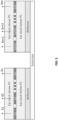
- FIG. 1 illustrates a first example top emitter structure with a PCSEL, in accordance with various example implementations of this disclosure.
- the photonic crystal (PC) lattices L1, L2... Ln are designed to output wavelengths ⁇ 1, ⁇ 2... ⁇ n, respectively.
- the horizontal mode may be constrained by the lattice.
- the epi stacks (above and/or below the PC) may include a p-n junction.
- FIG. 2 illustrates an example bottom emitter structure with a PCSEL, in accordance with various example implementations of this disclosure.
- the PC lattices L1, L2... Ln are designed to output wavelengths ⁇ 1, ⁇ 2... ⁇ n, respectively.
- the horizontal mode may be constrained by the lattice.
- the epi stack above the PC may comprise a top distributed Bragg reflector (DBR) that is 100% reflective.
- the epi stack below the PC may comprise a bottom DBR that is not fully reflective.
- DBR distributed Bragg reflector
- FIG. 3 illustrates a second example top emitter structure with a PCSEL, in accordance with various example implementations of this disclosure.
- the PC lattices L1, L2... Ln are designed to output wavelengths ⁇ 1, ⁇ 2... ⁇ n, respectively.
- the horizontal mode, in FIG. 3 is constrained by the edge lattice (Le).
- the edge lattice allows for an OA ⁇ 30 ⁇ m.
- the edge lattice may also be used for smaller apertures in the bottom emitting configuration of FIG. 2 .
- FIG. 4 illustrates a third example top emitter structure with a PCSEL, in accordance with various example implementations of this disclosure.
- the PC lattices L1, L2... Ln are designed to output wavelengths ⁇ 1, ⁇ 2... ⁇ n, respectively.
- Optical elements (OE1, OE2, ..., OEn) are added in FIG. 4 .
- the optical elements may comprise lenses and/or diffusers that may be placed (e.g., etched, deposited) on the emission surface for beam shaping purposes.
- Horizontal modes in a PCSEL are constrained by the photonic crystal if the optical aperture is large (>30 ⁇ m), or by a secondary (outer) photonic crystal for smaller apertures ( ⁇ 30 ⁇ m).
- the photonic bandgap of the "outer" photonics crystal is smaller and hence it serves as a reflector.
- the epi stack for a p-n junction implementation consists of GaAs substrate and cladding layers.
- the photonic crystal layer can comprise GaAs or GaSb.
- the vertical mirror stack may comprise GaAs and AlGaAs mirrors that cover the required wavelength range. Additional lattice matching layers or wafer bonding may be required for the GaSb active region due to a lattice mismatch.
- the epi stack for InGaAs in the active region may comprise an InP substrate and cladding layers, a reflector, and a GalnAsP photonic crystal.
- At least two stack configurations are possible.
- One possible configuration comprises p on one side of the active region and n on the other.
- Another configuration comprises n on both sides of the active region and a tunnel junction (TJ) in between.
- TJ tunnel junction
- the PCSEL array can be manufactured monolithically for a range of wavelengths.
- the wavelength range in each monolithic array may depend on the uniformity requirements.
- the power uniformity across wavelengths depends on the gain peak of the active region material.
- the wavelength range may or may not cover the range between 2.0-2.4 ⁇ m. If the wavelength range does not cover the range between 2.0-2.4 ⁇ m, multiple, monolithic arrays may be used for the full range.
- the wavelength of each device in an array may be different and controlled by lithography (photonic crystal design). In such a case, the lattice constant will be different for each device.
- a vertical mirror stack may be shared between all the wavelengths or the subset of wavelengths depending on the uniformity requirements.
- the total response is a combination of the gain curve response and the mirror design and this feature may be used to design a "flat" response and hence a better uniformity.
- FIG. 5 illustrates an example structure that co-integrates two monolithic arrays, with different ranges of wavelengths, on the same substrate, in accordance with various example implementations of this disclosure.
- Each monolithic array could be integrated on the same platform through for example a pick and place process.
- Each monolithic array can have a separately optimized DBR stack. Due to the low spectral bandwidth of the PCSEL and the high central wavelength design accuracy, the achievable wavelength spacing can be ⁇ 5 nm.
- the monitoring system may be compatible with the integrated optics (i.e., deposited lenses and/or diffusers).
- the lasers in an array can be powered up simultaneously or sequentially.
- each laser can have an isolated metal contact and driver.
- Implementations as described herein may relate to the following: A glucose monitor with one or more photonic crystal surface-emitting lasers (PCSELs).
- the PCSEL comprises a plurality of photonics crystal sections. Each photonics crystal section is operable to emit light of a different wavelength. The horizontal emission by each photonics crystal section may be constrained by edge lattice sections.
- circuits and circuitry refer to physical electronic components (i.e. hardware) and any software and/or firmware ("code") which may configure the hardware, be executed by the hardware, and or otherwise be associated with the hardware.
- code software and/or firmware
- a particular processor and memory may comprise a first "circuit” when executing a first one or more lines of code and may comprise a second "circuit” when executing a second one or more lines of code.
- and/or means any one or more of the items in the list joined by “and/or”.
- x and/or y means any element of the three-element set ⁇ (x), (y), (x, y) ⁇ .
- x, y, and/or z means any element of the seven-element set ⁇ (x), (y), (z), (x, y), (x, z), (y, z), (x, y, z) ⁇ .
- exemplary means serving as a non-limiting example, instance, or illustration.
- e.g. and “for example” set off lists of one or more non-limiting examples, instances, or illustrations.
- circuitry is "operable" to perform a function whenever the circuitry comprises the necessary hardware and code (if any is necessary) to perform the function, regardless of whether performance of the function is disabled or not enabled (e.g., by a user-configurable setting, factory trim, etc.).
- based on means “based at least in part on.” For example, "x based on y” means that "x” is based at least in part on “y” (and may also be based on z, for example).
Landscapes
- Physics & Mathematics (AREA)
- General Physics & Mathematics (AREA)
- Optics & Photonics (AREA)
- Electromagnetism (AREA)
- Condensed Matter Physics & Semiconductors (AREA)
- Analytical Chemistry (AREA)
- General Health & Medical Sciences (AREA)
- Biochemistry (AREA)
- Immunology (AREA)
- Pathology (AREA)
- Chemical & Material Sciences (AREA)
- Life Sciences & Earth Sciences (AREA)
- Health & Medical Sciences (AREA)
- Semiconductor Lasers (AREA)
- Lasers (AREA)
- Measurement Of The Respiration, Hearing Ability, Form, And Blood Characteristics Of Living Organisms (AREA)
- Investigating Or Analysing Materials By Optical Means (AREA)
Abstract
Description
- This application claims the benefit of and priority to
U.S. Provisional Patent Application No. 63/519,805, titled "PCSEL FOR GLUCOSE MONITORING," filed August 15, 2023 - Limitations and disadvantages of traditional systems and methods for glucose monitoring will become apparent to one of skill in the art, through comparison of such approaches with some aspects of the present method and system set forth in the remainder of this disclosure with reference to the drawings.
- The systems and methods disclosed herein use a Photonic Crystal Surface-Emitting Laser (PCSEL) to monitor glucose, substantially as illustrated by and/or described in connection with at least one of the figures, as set forth more completely in the claims.
-
-
FIG. 1 illustrates a first example top emitter structure with a PCSEL, in accordance with various example implementations of this disclosure. -
FIG. 2 illustrates an example bottom emitter structure with a PCSEL, in accordance with various example implementations of this disclosure. -
FIG. 3 illustrates a second example top emitter structure with a PCSEL, in accordance with various example implementations of this disclosure. -
FIG. 4 illustrates a third example top emitter structure with a PCSEL, in accordance with various example implementations of this disclosure. -
FIG. 5 illustrates an example structure that co-integrates two monolithic arrays, with different ranges of wavelengths, on the same substrate, in accordance with various example implementations of this disclosure. - Millions of people have diabetes and require glucose level monitoring multiple times a day. However, monitoring systems that are available today are invasive. While monitoring systems today may use lasers, these systems are not adequate. For example, known existing solutions with a 2.0-2.4 µm laser source include bulk lasers (such as an excimer laser) that are not applicable for the compact wearable glucose sensor application. Another existing solution includes distributed-feedback laser (DFB) lasers. In a glucose level monitoring application with DFB lasers, the epi stack for each wavelength is different and the DFB lasers must be integrated on the same platform. This integration limits the number of wavelengths one can use with high yield, which also makes such a solution expensive. Additionally, existing solutions have a relatively broad spectral bandwidth (SBW) for each wavelength (e.g., ~1 nm) and a low beam quality (e.g., M2 > 1.1). While tunable lasers are also compatible with the 2.0-2.4 µm range emission, precise wavelength tuning of the laser is very difficult.
- This disclosure describes a non-invasive system and method to monitor glucose. As described below, in accordance with various example implementations of this disclosure, a 2.0-2.4 µm Photonic Crystal Surface-Emitting Laser (PCSEL) may be used for non-invasive glucose monitoring and other medical optical sensing applications. The PCSEL provides superior beam purity and superior beam quality for such optical sensing applications. Additionally, the PCSEL enables a monolithic integration for a range of wavelengths that may be required for an absorption-based glucose sensing application.
- The PCSEL's emission wavelength is defined through the photonic crystal lattice design and may be limited by the etching tool capability. The wavelength precision is significantly better than existing solutions. PCSELs have a significantly lower SBW (e.g., <0.1 nm) and a superior beam quality (e.g., M2 < 1.1). PCSELs enable monolithic integration for a larger number of wavelengths. Therefore, a single epi design may be used for multiple wavelengths.
- While this disclosure describes using monolithic PCSEL arrays for glucose monitoring with wavelengths between 2.0-2.4 µm, other wavelength ranges may also be supported by using a different material set for the active region. For example, for wavelengths between 2.0-2.4 µm, highly strained InGaAs and GaSb materials may be used for the active region as the gain of InGaAs and GaSb supports this wavelength range.
- The PCSEL emission direction can be either top (
FIGs. 1 ,3 ,4 and5 ) or bottom (FIG. 2 ), depending on the application requirements. -
FIG. 1 illustrates a first example top emitter structure with a PCSEL, in accordance with various example implementations of this disclosure. - The photonic crystal (PC) lattices L1, L2... Ln are designed to output wavelengths λ1, λ2... λn, respectively. For a large optical aperture (e.g., OA > 30 µm), the horizontal mode may be constrained by the lattice. The epi stacks (above and/or below the PC) may include a p-n junction.
-
FIG. 2 illustrates an example bottom emitter structure with a PCSEL, in accordance with various example implementations of this disclosure. - As in
FIG. 1 , the PC lattices L1, L2... Ln are designed to output wavelengths λ1, λ2... λn, respectively. For a large optical aperture (e.g., OA > 30 µm), the horizontal mode may be constrained by the lattice. The epi stack above the PC may comprise a top distributed Bragg reflector (DBR) that is 100% reflective. The epi stack below the PC may comprise a bottom DBR that is not fully reflective. -
FIG. 3 illustrates a second example top emitter structure with a PCSEL, in accordance with various example implementations of this disclosure. - As in
FIGs. 1 and2 , the PC lattices L1, L2... Ln are designed to output wavelengths λ1, λ2... λn, respectively. The horizontal mode, inFIG. 3 , is constrained by the edge lattice (Le). The edge lattice allows for an OA < 30 µm. The edge lattice may also be used for smaller apertures in the bottom emitting configuration ofFIG. 2 . -
FIG. 4 illustrates a third example top emitter structure with a PCSEL, in accordance with various example implementations of this disclosure. - As in
FIGs. 1-3 , the PC lattices L1, L2... Ln are designed to output wavelengths λ1, λ2... λn, respectively. Optical elements (OE1, OE2, ..., OEn) are added inFIG. 4 . The optical elements may comprise lenses and/or diffusers that may be placed (e.g., etched, deposited) on the emission surface for beam shaping purposes. - Horizontal modes in a PCSEL are constrained by the photonic crystal if the optical aperture is large (>30 µm), or by a secondary (outer) photonic crystal for smaller apertures (<30 µm). The photonic bandgap of the "outer" photonics crystal is smaller and hence it serves as a reflector.
- For the GaSb in the active region, the epi stack for a p-n junction implementation consists of GaAs substrate and cladding layers. The photonic crystal layer can comprise GaAs or GaSb.
- The vertical mirror stack may comprise GaAs and AlGaAs mirrors that cover the required wavelength range. Additional lattice matching layers or wafer bonding may be required for the GaSb active region due to a lattice mismatch.
- For the solution with strained InGaAs in the active region, regrowth may be used to form the photonic crystal and epi layers above it. The epi stack for InGaAs in the active region may comprise an InP substrate and cladding layers, a reflector, and a GalnAsP photonic crystal.
- For both GaSb and InGaAs solutions, at least two stack configurations are possible. One possible configuration comprises p on one side of the active region and n on the other. Another configuration comprises n on both sides of the active region and a tunnel junction (TJ) in between.
- The PCSEL array can be manufactured monolithically for a range of wavelengths. The wavelength range in each monolithic array may depend on the uniformity requirements. The power uniformity across wavelengths depends on the gain peak of the active region material. The wavelength range may or may not cover the range between 2.0-2.4 µm. If the wavelength range does not cover the range between 2.0-2.4 µm, multiple, monolithic arrays may be used for the full range.
- The wavelength of each device in an array may be different and controlled by lithography (photonic crystal design). In such a case, the lattice constant will be different for each device.
- A vertical mirror stack may be shared between all the wavelengths or the subset of wavelengths depending on the uniformity requirements. The total response is a combination of the gain curve response and the mirror design and this feature may be used to design a "flat" response and hence a better uniformity.
-
FIG. 5 illustrates an example structure that co-integrates two monolithic arrays, with different ranges of wavelengths, on the same substrate, in accordance with various example implementations of this disclosure. - Multiple monolithic arrays could be integrated on the same platform through for example a pick and place process. Each monolithic array can have a separately optimized DBR stack. Due to the low spectral bandwidth of the PCSEL and the high central wavelength design accuracy, the achievable wavelength spacing can be <5 nm.
- Wavelengths may also be spaced over temperature. The central wavelength of each device may have the same thermal shift. The index of refraction may change with temperature. For example, the index of refraction may change by 0.07 nm for every degree Celsius. The relative wavelength spacing may be maintained over temperature. Therefore, the glucose monitoring application with PCSELs may not need cooling. The wavelength spacing may depend on the etching capability.
- The monitoring system may be compatible with the integrated optics (i.e., deposited lenses and/or diffusers). The lasers in an array can be powered up simultaneously or sequentially. To support the sequential wavelength sweep, each laser can have an isolated metal contact and driver.
- In the following, a set of aspects is disclosed. The aspects are numbered to facilitate referencing the features of one aspect in other aspects. The aspects form part of the disclosure of the present application and could be made subject to independent and/or dependent claims irrespective of what currently is claimed in the application. The aspects are:
- 1. A laser device, comprising:
- a first photonics crystal section operable to out-couple light, of a first wavelength, in a vertical direction; and
- a second photonics crystal section operable to out-couple light, of a second wavelength that is different than the first wavelength, in the vertical direction.
- 2. The laser device of
aspect 1, wherein:
the first photonics crystal section and the second photonics crystal section are located at a same fabrication layer. - 3. The laser device of
aspect 1, wherein the laser device comprises:- a first epitaxy layer operably coupled below the first photonics crystal section and the second photonics crystal section, and
- a second epitaxy layer operably coupled below the first photonics crystal section and the second photonics crystal section.
- 4. The laser device of
aspect 1, wherein a glucose monitor comprises the laser device. - 5. The laser device of
aspect 1, wherein the laser device is a bottom-emitting laser. - 6. The laser device of
aspect 1, wherein the laser device is a top-emitting laser. - 7. The laser device of
aspect 1, wherein the first wavelength and the second wavelength are between 2.0 and 2.4 µm. - 8. The laser device of
aspect 1, wherein:- one or more edge lattice sections, adjacent to the first photonics crystal section, are operable to constrain a horizontal mode of the first wavelength, and
- one or more edge lattice sections, adjacent to the second photonics crystal section, are operable to constrain a horizontal mode of the second wavelength.
- 9. The laser device of
aspect 1, wherein the laser device comprises:
one or more optical elements placed on an emission surface. - 10. The laser device of
aspect 1, wherein:
the first wavelength and the second wavelength are determined according to temperature. - 11. A method of fabricating a laser device, comprising:
- fabricating a first photonics crystal section operable to out-couple light, of a first wavelength, in a vertical direction; and
- fabricating a second photonics crystal section operable to out-couple light, of a second wavelength that is different than the first wavelength, in the vertical direction.
- 12. The method of aspect 11, wherein:
the first photonics crystal section and the second photonics crystal section are located at a same fabrication layer. - 13. The method of aspect 11, wherein the method comprises:
- fabricating a first epitaxy layer operably prior to fabricating the first photonics crystal section and the second photonics crystal section, and
- fabricating a second epitaxy layer atop the first photonics crystal section and the second photonics crystal section.
- 14. The method of aspect 11, wherein a glucose monitor comprises the laser device.
- 15. The method of aspect 11, wherein the laser device is a bottom-emitting laser.
- 16. The method of aspect 11, wherein the laser device is a top-emitting laser.
- 17. The method of aspect 11, wherein the first wavelength and the second wavelength are between 2.0 and 2.4 µm.
- 18. The method of aspect 11, wherein the method comprises:
- fabricating one or more edge lattice sections, adjacent to the first photonics crystal section, are operable to constrain a horizontal mode of the first wavelength, and
- fabricating one or more edge lattice sections, adjacent to the second photonics crystal section, are operable to constrain a horizontal mode of the second wavelength.
- 19. The method of aspect 11, wherein the method comprises:
- placing one or more optical elements on an emission surface.
- 20. The method of aspect 11, wherein:
- the first wavelength and the second wavelength are determined according to temperature.
- Implementations as described herein may relate to the following: A glucose monitor with one or more photonic crystal surface-emitting lasers (PCSELs). The PCSEL comprises a plurality of photonics crystal sections. Each photonics crystal section is operable to emit light of a different wavelength. The horizontal emission by each photonics crystal section may be constrained by edge lattice sections.
- The present application claims priority of
U.S. Provisional Patent Application No. 63/519,805, filed August 15, 2023 U.S. Patent Application No. 18/739,612, filed June 11, 2024 - As used herein the terms "circuits" and "circuitry" refer to physical electronic components (i.e. hardware) and any software and/or firmware ("code") which may configure the hardware, be executed by the hardware, and or otherwise be associated with the hardware. As used herein, for example, a particular processor and memory may comprise a first "circuit" when executing a first one or more lines of code and may comprise a second "circuit" when executing a second one or more lines of code. As used herein, "and/or" means any one or more of the items in the list joined by "and/or". As an example, "x and/or y" means any element of the three-element set {(x), (y), (x, y)}. As another example, "x, y, and/or z" means any element of the seven-element set {(x), (y), (z), (x, y), (x, z), (y, z), (x, y, z)}. As used herein, the term "exemplary" means serving as a non-limiting example, instance, or illustration. As used herein, the terms "e.g.," and "for example" set off lists of one or more non-limiting examples, instances, or illustrations. As used herein, circuitry is "operable" to perform a function whenever the circuitry comprises the necessary hardware and code (if any is necessary) to perform the function, regardless of whether performance of the function is disabled or not enabled (e.g., by a user-configurable setting, factory trim, etc.). As used herein, the term "based on" means "based at least in part on." For example, "x based on y" means that "x" is based at least in part on "y" (and may also be based on z, for example).
- While the present method and/or system has been described with reference to certain implementations, it will be understood by those skilled in the art that various changes may be made and equivalents may be substituted without departing from the scope of the present method and/or system. In addition, many modifications may be made to adapt a particular situation or material to the teachings of the present disclosure without departing from its scope. Therefore, it is intended that the present method and/or system not be limited to the particular implementations disclosed, but that the present method and/or system will include all implementations falling within the scope of the appended claims.
Claims (15)
- A laser device, comprising:a first photonics crystal section operable to out-couple light, of a first wavelength, in a vertical direction; anda second photonics crystal section operable to out-couple light, of a second wavelength that is different than the first wavelength, in the vertical direction.
- The laser device of claim 1, wherein:
the first photonics crystal section and the second photonics crystal section are located at a same fabrication layer. - The laser device of any one of the preceding claims, wherein the laser device comprises:a first epitaxy layer operably coupled below the first photonics crystal section and the second photonics crystal section, anda second epitaxy layer operably coupled below the first photonics crystal section and the second photonics crystal section.
- The laser device of any one of the preceding claims, wherein a glucose monitor comprises the laser device.
- The laser device of any one of the preceding claims, wherein the laser device is a bottom-emitting laser or a top-emitting laser.
- The laser device of any one of the preceding claims, wherein the first wavelength and the second wavelength are between 2.0 and 2.4 µm.
- The laser device of any one of the preceding claims, wherein:one or more edge lattice sections, adjacent to the first photonics crystal section, are operable to constrain a horizontal mode of the first wavelength, andone or more edge lattice sections, adjacent to the second photonics crystal section, are operable to constrain a horizontal mode of the second wavelength.
- The laser device of any one of the preceding claims, wherein the laser device comprises:one or more optical elements placed on an emission surface, and/or, whereinthe first wavelength and the second wavelength are determined according to temperature.
- A method of fabricating a laser device, comprising:fabricating a first photonics crystal section operable to out-couple light, of a first wavelength, in a vertical direction; andfabricating a second photonics crystal section operable to out-couple light, of a second wavelength that is different than the first wavelength, in the vertical direction.
- The method of claim 9, wherein:
the first photonics crystal section and the second photonics crystal section are located at a same fabrication layer. - The method of any one of the preceding claims 9 to 10, wherein the method comprises:fabricating a first epitaxy layer operably prior to fabricating the first photonics crystal section and the second photonics crystal section, andfabricating a second epitaxy layer atop the first photonics crystal section and the second photonics crystal section.
- The method of any one of the preceding claims 9 to 11, wherein a glucose monitor comprises the laser device.
- The method of any one of the preceding claims 9 to 11, wherein the laser device is a bottom-emitting laser or a top-emitting laser.
- The method of any one of the preceding claims 9 to 13, wherein the first wavelength and the second wavelength are between 2.0 and 2.4 µm.
- The method of any one of the preceding claims 9 to 14, wherein the method comprises:fabricating one or more edge lattice sections, adjacent to the first photonics crystal section, are operable to constrain a horizontal mode of the first wavelength, andfabricating one or more edge lattice sections, adjacent to the second photonics crystal section, are operable to constrain a horizontal mode of the second wavelength, wherein the method optionally further comprises:i) placing one or more optical elements on an emission surface, and/or whereinii) the first wavelength and the second wavelength are determined according to temperature.
Applications Claiming Priority (2)
| Application Number | Priority Date | Filing Date | Title |
|---|---|---|---|
| US202363519805P | 2023-08-15 | 2023-08-15 | |
| US18/739,612 US20250062595A1 (en) | 2023-08-15 | 2024-06-11 | Pcsel for glucose monitoring |
Publications (2)
| Publication Number | Publication Date |
|---|---|
| EP4510398A2 true EP4510398A2 (en) | 2025-02-19 |
| EP4510398A3 EP4510398A3 (en) | 2025-03-12 |
Family
ID=92295743
Family Applications (1)
| Application Number | Title | Priority Date | Filing Date |
|---|---|---|---|
| EP24193472.8A Pending EP4510398A3 (en) | 2023-08-15 | 2024-08-08 | Pcsel for glucose monitoring |
Country Status (4)
| Country | Link |
|---|---|
| US (1) | US20250062595A1 (en) |
| EP (1) | EP4510398A3 (en) |
| JP (1) | JP7892025B2 (en) |
| CN (1) | CN119492708A (en) |
Family Cites Families (7)
| Publication number | Priority date | Publication date | Assignee | Title |
|---|---|---|---|---|
| JPH09219563A (en) * | 1996-02-09 | 1997-08-19 | Hitachi Ltd | Semiconductor optical device and application system using the same |
| JP2010093127A (en) * | 2008-10-09 | 2010-04-22 | Sumitomo Electric Ind Ltd | Semiconductor light emitting device |
| WO2012134515A1 (en) * | 2011-04-01 | 2012-10-04 | Verifica-Bg Inc. | Method and apparatus for in vivo optical measurement of blood glucose concentration |
| JP6807643B2 (en) * | 2016-01-08 | 2021-01-06 | 浜松ホトニクス株式会社 | Distribution feedback type semiconductor laser device |
| JP7306675B2 (en) * | 2019-02-22 | 2023-07-11 | 国立大学法人京都大学 | Two-dimensional photonic crystal surface emitting laser |
| US20220344905A1 (en) * | 2021-04-21 | 2022-10-27 | Osram Opto Semiconductors Gmbh | Semiconductor laser device and projection device |
| JP7690355B2 (en) * | 2021-08-27 | 2025-06-10 | 株式会社東芝 | Analyzer |
-
2024
- 2024-06-11 US US18/739,612 patent/US20250062595A1/en active Pending
- 2024-07-30 JP JP2024123052A patent/JP7892025B2/en active Active
- 2024-08-08 EP EP24193472.8A patent/EP4510398A3/en active Pending
- 2024-08-14 CN CN202411114944.1A patent/CN119492708A/en active Pending
Also Published As
| Publication number | Publication date |
|---|---|
| US20250062595A1 (en) | 2025-02-20 |
| JP7892025B2 (en) | 2026-07-17 |
| CN119492708A (en) | 2025-02-21 |
| EP4510398A3 (en) | 2025-03-12 |
| JP2025027994A (en) | 2025-02-28 |
Similar Documents
| Publication | Publication Date | Title |
|---|---|---|
| EP1097394B1 (en) | External cavity laser | |
| US5953362A (en) | Strain induce control of polarization states in vertical cavity surface emitting lasers and method of making same | |
| EP1363370B1 (en) | Fixed wavelength vertical cavity optical devices and method of manufacture thereof | |
| US10476233B2 (en) | Ultra-low noise, highly stable single-mode operation, high power, Bragg grating based semiconductor laser | |
| US20150311673A1 (en) | Polarization Control in High Peak Power, High Brightness VCSEL | |
| US20080075133A1 (en) | Extended tuning in external cavity quantum cascade lasers | |
| US7221828B2 (en) | Optical wave length division multiplexing module and communication system using the same | |
| US8902944B2 (en) | High power multi-wavelength laser source | |
| US20130077648A1 (en) | Surface emitting semiconductor laser and method of manufacture thereof | |
| US20100142579A1 (en) | Resonator of hybrid laser diode | |
| US20050074197A1 (en) | Integrated surface emitting laser and light amplifier | |
| US20250062595A1 (en) | Pcsel for glucose monitoring | |
| JP7109241B2 (en) | OPTO-SEMICONDUCTOR DEVICE AND METHOD FOR MANUFACTURING OPTO-SEMICONDUCTOR DEVICE | |
| US20020159491A1 (en) | Surface emitting laser | |
| GB2396054A (en) | Semiconductor optical device with beam focusing | |
| US20220029378A1 (en) | Optical waveguide device and laser apparatus including the same | |
| WO2003012832A2 (en) | Multiple epitaxial region substrate and technique for making the same | |
| Pissis et al. | Monolithic multiwavelength VCSEL array with intra-cavity grating | |
| US20250329987A1 (en) | Tunable laser with improved stability | |
| US7065120B2 (en) | Integrated laser with Perot-Fabry cavity | |
| WO2025136079A1 (en) | External cavity laser and integration process for making the same | |
| KR100212460B1 (en) | Long wavelength surface emitting laser chip and its manufacturing method | |
| US20110176204A1 (en) | Photo-pumped semiconductor optical amplifier | |
| JP2001024287A (en) | Semiconductor laser optical module for WDM | |
| JPH03225886A (en) | Surface emission semiconductor laser array |
Legal Events
| Date | Code | Title | Description |
|---|---|---|---|
| PUAI | Public reference made under article 153(3) epc to a published international application that has entered the european phase |
Free format text: ORIGINAL CODE: 0009012 |
|
| STAA | Information on the status of an ep patent application or granted ep patent |
Free format text: STATUS: REQUEST FOR EXAMINATION WAS MADE |
|
| PUAL | Search report despatched |
Free format text: ORIGINAL CODE: 0009013 |
|
| 17P | Request for examination filed |
Effective date: 20240808 |
|
| AK | Designated contracting states |
Kind code of ref document: A2 Designated state(s): AL AT BE BG CH CY CZ DE DK EE ES FI FR GB GR HR HU IE IS IT LI LT LU LV MC ME MK MT NL NO PL PT RO RS SE SI SK SM TR |
|
| AK | Designated contracting states |
Kind code of ref document: A3 Designated state(s): AL AT BE BG CH CY CZ DE DK EE ES FI FR GB GR HR HU IE IS IT LI LT LU LV MC ME MK MT NL NO PL PT RO RS SE SI SK SM TR |
|
| RIC1 | Information provided on ipc code assigned before grant |
Ipc: A61B 5/145 20060101ALN20250203BHEP Ipc: H01S 5/42 20060101ALI20250203BHEP Ipc: H01S 5/40 20060101ALI20250203BHEP Ipc: H01S 5/20 20060101ALI20250203BHEP Ipc: H01S 5/183 20060101ALI20250203BHEP Ipc: H01S 5/11 20210101AFI20250203BHEP |
|
| P01 | Opt-out of the competence of the unified patent court (upc) registered |
Free format text: CASE NUMBER: APP_8702/2025 Effective date: 20250220 |