EP4510191A1 - Light detection device - Google Patents
Light detection device Download PDFInfo
- Publication number
- EP4510191A1 EP4510191A1 EP23791728.1A EP23791728A EP4510191A1 EP 4510191 A1 EP4510191 A1 EP 4510191A1 EP 23791728 A EP23791728 A EP 23791728A EP 4510191 A1 EP4510191 A1 EP 4510191A1
- Authority
- EP
- European Patent Office
- Prior art keywords
- pair
- mounting region
- detection device
- receiving element
- edges
- Prior art date
- Legal status (The legal status is an assumption and is not a legal conclusion. Google has not performed a legal analysis and makes no representation as to the accuracy of the status listed.)
- Pending
Links
Images


Classifications
-
- H—ELECTRICITY
- H10—SEMICONDUCTOR DEVICES; ELECTRIC SOLID-STATE DEVICES NOT OTHERWISE PROVIDED FOR
- H10F—INORGANIC SEMICONDUCTOR DEVICES SENSITIVE TO INFRARED RADIATION, LIGHT, ELECTROMAGNETIC RADIATION OF SHORTER WAVELENGTH OR CORPUSCULAR RADIATION
- H10F39/00—Integrated devices, or assemblies of multiple devices, comprising at least one element covered by group H10F30/00, e.g. radiation detectors comprising photodiode arrays
- H10F39/10—Integrated devices
- H10F39/12—Image sensors
- H10F39/18—Complementary metal-oxide-semiconductor [CMOS] image sensors; Photodiode array image sensors
- H10F39/189—X-ray, gamma-ray or corpuscular radiation imagers
- H10F39/1898—Indirect radiation image sensors, e.g. using luminescent members
-
- G—PHYSICS
- G01—MEASURING; TESTING
- G01T—MEASUREMENT OF NUCLEAR OR X-RADIATION
- G01T1/00—Measuring X-radiation, gamma radiation, corpuscular radiation, or cosmic radiation
- G01T1/16—Measuring radiation intensity
- G01T1/20—Measuring radiation intensity with scintillation detectors
- G01T1/2018—Scintillation-photodiode combinations
-
- H—ELECTRICITY
- H10—SEMICONDUCTOR DEVICES; ELECTRIC SOLID-STATE DEVICES NOT OTHERWISE PROVIDED FOR
- H10F—INORGANIC SEMICONDUCTOR DEVICES SENSITIVE TO INFRARED RADIATION, LIGHT, ELECTROMAGNETIC RADIATION OF SHORTER WAVELENGTH OR CORPUSCULAR RADIATION
- H10F39/00—Integrated devices, or assemblies of multiple devices, comprising at least one element covered by group H10F30/00, e.g. radiation detectors comprising photodiode arrays
- H10F39/80—Constructional details of image sensors
- H10F39/804—Containers or encapsulations
-
- H—ELECTRICITY
- H10—SEMICONDUCTOR DEVICES; ELECTRIC SOLID-STATE DEVICES NOT OTHERWISE PROVIDED FOR
- H10F—INORGANIC SEMICONDUCTOR DEVICES SENSITIVE TO INFRARED RADIATION, LIGHT, ELECTROMAGNETIC RADIATION OF SHORTER WAVELENGTH OR CORPUSCULAR RADIATION
- H10F77/00—Constructional details of devices covered by this subclass
- H10F77/93—Interconnections
Definitions
- the present disclosure relates to a light detection device.
- a light detection device including a wiring substrate, a light receiving element mounted on the wiring substrate, and a connection member electrically connecting the wiring substrate and the light receiving element is known (see, for example, Patent Literature 1).
- a radiation detection unit used in a CT device or the like there is a case where a plurality of such light detection devices is arranged in a state where an interval between the light detection devices is reduced.
- Patent Literature 1 Japanese Unexamined Patent Publication No. 2015-000291
- a film-shaped adhesive member may be disposed between the wiring substrate and the light receiving element.
- the film-shaped adhesive member when the film-shaped adhesive member is disposed in the entire region between the wiring substrate and the light receiving element at the time of manufacturing in order to realize stable bonding between the wiring substrate and the light receiving element, the film-shaped adhesive member projects from the region between the wiring substrate and the light receiving element, and it may be difficult to arrange the plurality of light detection devices in a state where the interval between the light detection devices is reduced.
- An object of the present disclosure is to provide a light detection device capable of realizing stable bonding between a wiring substrate and a light receiving element while preventing projection of a film-shaped adhesive member.
- a light detection device including a wiring substrate, a light receiving element mounted on the wiring substrate, a connection member electrically connecting the wiring substrate and the light receiving element, and a film-shaped adhesive member bonding the wiring substrate and the light receiving element, in which a mounting region where the wiring substrate and the light receiving element overlap when viewed from a first direction in which the wiring substrate and the light receiving element are arranged has a pair of first sides facing each other in a second direction perpendicular to the first direction and a pair of second sides facing each other in a third direction perpendicular to the first direction and the second direction, and the film-shaped adhesive member is disposed in the mounting region when viewed from the first direction, and the film-shaped adhesive member includes a main body portion having a pair of first edges extending so as to notch the mounting region on a center side of the mounting region in each of the pair of first sides and a pair of second edges extending so as to notch the mounting region on the center side of the mounting
- the film-shaped adhesive member disposed in the mounting region includes a main body portion having a shape notched on each side of the mounting region. This makes it less likely for the film-shaped adhesive member to project from the mounting region at the time of bonding the wiring substrate and the light receiving element. Further, the main body portion of the film-shaped adhesive member extends to each corner portion of the mounting region, and the film-shaped adhesive member disposed in the mounting region further includes at least one projecting portion extending from at least one edge of the main body portion. As a result, the interval between the wiring substrate and the light receiving element is easily kept constant at the time of bonding the wiring substrate and the light receiving element, and as a result, the wiring substrate and the light receiving element are firmly bonded. Therefore, according to the light detection device of [1] described above, it is possible to realize stable bonding between a wiring substrate and a light receiving element while preventing projection of a film-shaped adhesive member.
- a light detection device may be [2] "The light detection device according to [1] described above, in which the at least one projecting portion extends from each of the pair of first edges and each of the pair of second edges to the side opposite to the center of the mounting region.” According to the light detection device of [2], stable bonding between the wiring substrate and the light receiving element can be more reliably realized.
- a light detection device may be [3] "The light detection device according to [1] or [2] described above, in which each of the pair of first edges and each of the pair of second edges extends along a curve recessed toward the center side of the mounting region.”
- the film-shaped adhesive member easily projects at the center of each side of the mounting region, but according to the light detection device of [3], projection of the film-shaped adhesive member at the center of each side of the mounting region can be more reliably prevented.
- a light detection device may be [4] "The light detection device according to any one of [1] to [3] described above, in which the film-shaped adhesive member includes a plurality of projecting portions as the at least one projecting portion, the plurality of projecting portions extending from each of the pair of first edges and each of the pair of second edges to the side opposite to the center of the mounting region.” According to the light detection device of [4] described above, it is possible to more reliably realize stable bonding between a wiring substrate and a light receiving element while preventing more reliably projection of a film-shaped adhesive member.
- a light detection device may be [5] "The light detection device according to [4] described above, in which the plurality of projecting portions includes a first projecting portion, and a second projecting portion having a width larger than a width of the first projecting portion.”
- the defect of each projecting portion is suppressed so that stable bonding between the wiring substrate and the light receiving element can be realized.
- the yield is improved.
- a light detection device may be [6] "The light detection device according to [4] or [5] described above, in which the plurality of projecting portions includes a plurality of third projecting portions extending to the side opposite to the center of the mounting region at a center of each of the pair of first edges and each of the pair of second edges, and a plurality of fourth projecting portions extending to the side opposite to the center of the mounting region on both sides of the center of each of the pair of first edges and each of the pair of second edges, and each of the third projecting portions has a length longer than a length of each of the fourth projecting portions.”
- the film-shaped adhesive member easily projects at the center of each side of the mounting region, but according to the light detection device of [6], since the retraction amount of each edge of the main body portion increases at the center of each side of the mounting region, projection of the film-shaped adhesive member at the center of each side of the mounting region can be more reliably prevented.
- the defect of each projecting portion is suppressed so that stable bonding between the wiring substrate and the light receiving element can be realized.
- the yield is improved.
- a light detection device may be [7] "The light detection device according to any one of [1] to [6], in which the connection member is each of a plurality of connection members arranged two-dimensionally.” According to the light detection device of [7] described above, for example, even in a case where an area sensor is used as a light receiving element, it is possible to realize stable bonding between a wiring substrate and a light receiving element while preventing projection of a film-shaped adhesive member.
- a light detection device may be [8] "The light detection device according to [7], in which the main body portion and the at least one projecting portion overlap the plurality of connection members when viewed from the first direction.” According to the light detection device of [8], since each connection member is reinforced by the film-shaped adhesive member, electrical connection between the wiring substrate and the light receiving element by each connection member can be maintained in a reliable state.
- a light detection device may be [9] "The light detection device according to any one of [1] to [8], in which an outer edge of the film-shaped adhesive member is located inside an outer edge of the light receiving element when viewed from the first direction.” According to the light detection device of [9], projection of the film-shaped adhesive member can be more reliably prevented.
- a light detection device may be [10] "The light detection device according to any one of [1] to [9], in which a distance between the pair of second sides is larger than a distance between the pair of first sides.” According to the light detection device of [10] described above, for example, even in a case where a rectangular plate-shaped sensor using its longitudinal direction as the third direction is used as a light receiving element, it is possible to realize stable bonding between a wiring substrate and a light receiving element while preventing projection of a film-shaped adhesive member.
- a light detection device may be [11] "The light detection device according to [10], in which at least one slit extending from each of the pair of second edges to the center side of the mounting region is formed in the main body portion.”
- the length of the slit can be sufficiently secured in the pair of second edges having the interval larger than the interval between the pair of first edges, and the projection of the film-shaped adhesive member on each second side of the mounting region can be more reliably prevented.
- the defect of the main body portion is suppressed. Therefore, stable bonding between the wiring substrate and the light receiving element can be realized.
- a light detection device may be [12] "The light detection device according to any one of [1] to [11], in which the film-shaped adhesive member is an anisotropic conductive film.” According to the light detection device of [12], electrical connection between the wiring substrate and the light receiving element by each connection member can be maintained in a reliable state.
- a light detection device may be [13] "The light detection device according to any one of [1] to [12], further including a protection member extending along an outer edge of a region between the wiring substrate and the light receiving element.” According to the light detection device of [13], it is possible to suppress the occurrence of damage such as a defect in the light receiving element.
- a light detection device capable of realizing stable bonding between a wiring substrate and a light receiving element while preventing projection of a film-shaped adhesive member.
- a radiation detector 10 includes a light detection device 1, a scintillator layer 11, a plurality of integrated circuit devices 12, a flexible printed circuit substrate 13, and a heat sink 14.
- the radiation detector 10 when radiation (for example, ⁇ -rays, X-rays, and the like) enters the scintillator layer 11, scintillation light is generated in the scintillator layer 11, and the scintillation light is detected by the light detection device 1.
- the radiation detector 10 is used as a radiation imaging device, for example, in a medical radiological imaging apparatus, a nondestructive inspection apparatus, or the like.
- the light detection device 1 includes a wiring substrate 2, a light receiving element 3, a film-shaped adhesive member 4, a plurality of first connection members 6a, a plurality of second connection members 6b (see FIGS. 2 and 3 ), and a protection member 7.
- the wiring substrate 2 has a front surface 2a and a back surface 2b.
- the light receiving element 3 has a front surface 3a and a back surface 3b.
- the light receiving element 3 is mounted on the front surface 2a of the wiring substrate 2 with the back surface 3b of the light receiving element 3 facing the front surface 2a of the wiring substrate 2.
- the light receiving element 3 is a backside incidence type area sensor including a plurality of photodiodes (photoelectric conversion regions) arranged two-dimensionally.
- the first direction in which a wiring substrate and a light receiving element are arranged is referred to as a Z direction
- the second direction perpendicular to the first direction is referred to as an X direction
- the third direction perpendicular to the first direction and the second direction is referred to as a Y direction.
- the plurality of connection members 6a and 6b electrically connect the wiring substrate 2 and the light receiving element 3. Specifically, the plurality of connection members 6a and 6b electrically and physically connect the plurality of pads provided on the wiring substrate 2 and the plurality of electrodes provided on the light receiving element 3.
- each of the connection members 6a and 6b is a bump electrode.
- the film-shaped adhesive member 4 bonds the wiring substrate 2 and the light receiving element 3.
- the film-shaped adhesive member 4 is an anisotropic conductive film (ACF).
- the thickness of the film-shaped adhesive member 4 is, for example, 0.03 to 0.08 mm.
- the protection member 7 extends along the outer edge of the region between the wiring substrate 2 and the light receiving element 3. In the present embodiment, the protection member 7 surrounds the outer edge of the region between the wiring substrate 2 and the light receiving element 3 in a frame shape.
- the protection member 7 is formed of, for example, an underfill resin agent.
- the scintillator layer 11 is disposed on the front surface 3a of the light receiving element 3.
- the scintillator layer 11 is optically separated for each photodiode included in the light receiving element 3 when viewed from the Z direction.
- the material of the scintillator layer 11 is, for example, LYSO or the like in a case where a ⁇ -ray is to be detected, and is, for example, CsI, GOS, or the like in a case where an X-ray is to be detected.
- the plurality of integrated circuit devices 12 is mounted on the back surface 2b of the wiring substrate 2.
- Each integrated circuit device 12 is electrically and physically connected to the wiring substrate 2 by the plurality of bump electrodes 12a.
- the flexible printed circuit substrate 13 is electrically and physically connected to the wiring substrate 2 by the plurality of bump electrodes 13a.
- the operation of the light receiving element 3 is controlled by the plurality of integrated circuit devices 12, and the external input of the electric signal and the external output of the electric signal are performed by the flexible printed circuit substrate 13.
- the heat sink 14 is attached to the back surface 2b of the wiring substrate 2 in a state of being in contact with the plurality of integrated circuit devices 12. The heat sink 14 cools each integrated circuit device 12.
- the light receiving element 3 includes an n-type semiconductor substrate 30 made of silicon.
- the thickness of the n-type semiconductor substrate 30 is, for example, 30 to 300 ⁇ m.
- the impurity concentration of the n-type semiconductor substrate 30 is, for example, 1 ⁇ 10 12 to 1 ⁇ 10 15 /cm 3 .
- a plurality of p-type regions 31 is formed in a portion of the n-type semiconductor substrate 30 along the back surface 3b.
- the plurality of p-type regions 31 is two-dimensionally arranged with the X direction and the Y direction as a column direction and a row direction.
- the plurality of p-type regions 31 forms a plurality of pn junction regions with the n-type semiconductor substrate 30.
- the plurality of pn junction regions functions as a plurality of photodiodes.
- the width of each p-type region 31 in the Z direction is, for example, 0.05 to 20 ⁇ m.
- the impurity concentration of each p-type region 31 is, for example, 1 ⁇ 10 13 to 1 ⁇ 10 20 /cm 3 .
- a plurality of high-concentration n-type regions 32 is formed in a portion of the n-type semiconductor substrate 30 along the back surface 3b.
- Each of the high-concentration n-type region 32 extends in a frame shape so as to surround each of the p-type region 31 when viewed from the Z direction.
- the plurality of high-concentration n-type regions 32 electrically isolates the plurality of photodiodes from each other, thereby suppressing occurrence of crosstalk between adjacent photodiodes.
- the width of each high-concentration n-type region 32 in the Z direction is, for example, 0.1 to several tens of ⁇ m.
- the impurity concentration of each high-concentration n-type region 32 is, for example, 1 ⁇ 10 13 to 1 ⁇ 10 20 /cm 3 .
- a p-type region 33 is formed in a portion of the n-type semiconductor substrate 30 along the back surface 3b.
- the p-type region 33 extends in a lattice shape so as to pass between the adjacent high-concentration n-type regions 32 when viewed from the Z direction.
- the p-type region 33 forms a pn junction region with the n-type semiconductor substrate 30.
- the width of the p-type region 33 in the Z direction is, for example, 0.05 to 20 ⁇ m.
- the impurity concentration of the p-type region 33 is, for example, 1 ⁇ 10 13 to 1 ⁇ 10 20 /cm 3 .
- a plurality of first connection members 6a is formed on the back surface 3b of the light receiving element 3.
- Each first connection member 6a is formed on each anode electrode (not illustrated) electrically connected to each of the p-type region 31.
- Each of the anode electrode is formed on the back surface of the n-type semiconductor substrate 30 and is located on each of the p-type region 31.
- a plurality of second connection members 6b is formed on the back surface 3b of the light receiving element 3.
- Each of the second connection member 6b is formed on each anode electrode (not illustrated) electrically connected to the plurality of high-concentration n-type regions 32 and p-type regions 33.
- the cathode electrode is formed on the back surface of the n-type semiconductor substrate 30, and extends in a lattice shape so as to cover the plurality of high-concentration n-type regions 32 and p-type regions 33.
- the plurality of second connection members 6b is formed on a plurality of intersections of the cathode electrodes extending in a lattice shape.
- the plurality of second connection members 6b is not formed on all the intersections, but is formed on the plurality of intersections for every predetermined number of intersections in both the X direction and the Y direction (see FIG. 3 ).
- Each of the second connection members 6b is electrically connected to the ground potential via the wiring substrate 2.
- the film-shaped adhesive member 4 is disposed in the mounting region 5 when viewed from the Z direction.
- the mounting region 5 is a region where the wiring substrate 2 overlaps the light receiving element 3 when viewed from the Z direction.
- the mounting region 5 is a region where the back surface 3b of the light receiving element 3 (specifically, the back surface of the n-type semiconductor substrate 30) overlaps the front surface 2a of the wiring substrate 2(that is, the mounting surface of the wiring substrate 2) when viewed from the Z direction.
- the outer edge of the film-shaped adhesive member 4 when viewed from the Z direction, is located inside the outer edge of the light receiving element 3.
- the mounting region 5 has a pair of first sides 51a and 51b and a pair of second sides 52a and 52b.
- the pair of first sides 51a and 51b face each other in the X direction.
- the pair of second sides 52a and 52b face each other in the Y direction.
- the distance between the pair of second sides 52a and 52b is larger than the distance between the pair of first sides 51a and 51b.
- the length of each of the first sides 51a and 51b is, for example, 30 to 50 mm.
- the length of each of the second sides 52a and 52b is, for example, 15 to 25 mm.
- the mounting region 5 has a rectangular shape with the pair of first sides 51a and 51b as long sides and the pair of second sides 52a and 52b as short sides.
- the wiring substrate 2 and the light receiving element 3 also have substantially the same rectangular shape as the mounting region 5 when viewed from the Z direction.
- the light receiving element 3 is indicated by a two-dot chain line, and the protection member 7 is not illustrated.
- the film-shaped adhesive member 4 includes a main body portion 40.
- the main body portion 40 has a pair of first edges 41a and 41b and a pair of second edges 42a and 42b.
- the first edge 41a extends on the first side 51a toward a center 50 of the mounting region 5 so as to notch the mounting region 5. That is, the first edge 41a is located inside with respect to the first side 51a.
- the first edge 41b extends on the first side 51b toward the center 50 of the mounting region 5 so as to notch the mounting region 5. That is, the first edge 41b is located inside with respect to the first side 51b.
- the second edge 42a extends on the second side 52a toward the center 50 of the mounting region 5 so as to notch the mounting region 5.
- each of the edges 41a, 41b, 42a, and 42b extends along a curve (for example, a round smooth curve) recessed toward the center 50 of the mounting region 5.
- the main body portion 40 extends to each of the four corner portions 53 of the mounting region 5. In other words, the main body portion 40 is not notched at each of the four corner portions 53 of the mounting region 5.
- the film-shaped adhesive member 4 further includes a plurality of first projecting portions (projecting portions) 43 and a plurality of second projecting portions (projecting portions) 44.
- the plurality of projecting portions 43 and 44 are formed integrally with the main body portion 40.
- the second projecting portion 44 has a width larger than the width of the first projecting portion 43.
- the width of the first projecting portion 43 is the width of the first projecting portion 43 in a direction perpendicular to the direction in which the first projecting portion 43 extends when viewed from the Z direction.
- the width of the second projecting portion 44 is the width of the second projecting portion 44 in a direction perpendicular to the direction in which the second projecting portion 44 extends when viewed from the Z direction.
- the width of the first projecting portion 43 is, for example, 0.5 to 2 mm.
- the width of the second projecting portion 44 is, for example, 1.5 to 6 mm.
- a slit opening to the side opposite to the main body portion 40 is formed at a distal end portion (end portion on the side opposite to the main body portion 40) of each of the second projecting portions 44. Note that the slit that opens to the side opposite to the main body portion 40 does not need to be formed at the distal end portion of each of the second projecting portions 44.
- the plurality of projecting portions 43 and 44 extends along the X direction to the side opposite to the center 50 of the mounting region 5. From the first edge 41b of the main body portion 40, the plurality of projecting portions 43 and 44 extends along the X direction to the side opposite to the center 50 of the mounting region 5. In each of the first edges 41a and 41b, the plurality of projecting portions 43 and 44 is arranged in the Y direction at predetermined intervals such that the plurality of (for example, two) first projecting portions 43 is positioned between the adjacent second projecting portions 44.
- the predetermined interval is, for example, 0.5 to 2 mm.
- the length of each of the projecting portions 43 and 44 extending from the first edge 41a becomes longer toward the center of the first edge 41a.
- the length of each of the projecting portions 43 and 44 may continuously increase one by one or may gradually increase for multiple units as approaching the center of the first edge 41a.
- the length of each of the projecting portions 43 and 44 extending from the first edge 41b becomes longer toward the center of the first edge 41b.
- the length of each of the projecting portions 43 and 44 may continuously increase one by one or may gradually increase for multiple units as approaching the center of the first edge 41b.
- each of the plurality of projecting portions 43 and 44 extending to the side opposite to the center 50 of the mounting region 5 at the center of each of the first edges 41a and 41b has a length longer than the length of each of the plurality of projecting portions 43 and 44 extending to the side opposite to the center 50 of the mounting region 5 on both sides of the center of each of the first edges 41a and 41b (each of the plurality of projecting portions 43 and 44 can be regarded as fourth projecting portions).
- the plurality of projecting portions 43 and 44 extends along the Y direction to the side opposite to the center 50 of the mounting region 5. From the second edge 42b of the main body portion 40, the plurality of projecting portions 43 and 44 extends along the Y direction to the side opposite to the center 50 of the mounting region 5.
- the plurality of projecting portions 43 and 44 is arranged in the X direction at predetermined intervals such that the plurality of (for example, two) first projecting portions 43 is positioned between the adjacent second projecting portions 44.
- the predetermined interval is, for example, 0.5 to 2 mm.
- the length of each of the projecting portions 43 and 44 extending from the second edge 42a becomes longer toward the center of the second edge 42a.
- the length of each of the projecting portions 43 and 44 may continuously increase one by one or may gradually increase for multiple units as approaching the center of the second edge 42a.
- the length of each of the projecting portions 43 and 44 extending from the second edge 42b becomes longer toward the center of the second edge 42b.
- the length of each of the projecting portions 43 and 44 may continuously increase one by one or may gradually increase for multiple units as approaching the center of the second edge 42b.
- each of the plurality of projecting portions 43 and 44 extending to the side opposite to the center 50 of the mounting region 5 at the center of each of the second edges 42a and 42b has a length longer than the length of each of the plurality of projecting portions 43 and 44 extending to the side opposite to the center 50 of the mounting region 5 on both sides of the center of each of the second edges 42a and 42b (each of the plurality of projecting portions 43 and 44 can be regarded as fourth projecting portions).
- a pair of slits 40a and 40b is formed in the main body portion 40.
- the slit 40a extends from the second edge 42a toward the center 50 of the mounting region 5.
- the slit 40a extends along the Y direction from the center of the second edge 42a.
- the width of the slit 40a in the X direction is equal to a predetermined interval between the projecting portions 43 and 44 adjacent along the second edge 42a, and the length of the slit 40a in the Y direction is longer than the length of each of the projecting portions 43 and 44 extending from the second edge 42a.
- the slit 40b extends from the second edge 42b toward the center 50 of the mounting region 5.
- the slit 40b extends along the Y direction from the center of the second edge 42b.
- the width of the slit 40b in the X direction is equal to a predetermined interval between the projecting portions 43 and 44 adjacent along the second edge 42b, and the length of the slit 40b in the Y direction is longer than the length of each of the projecting portions 43 and 44 extending from the second edge 42b.
- the film-shaped adhesive member 4 has a point-symmetrical shape with the center 50 of the mounting region 5 as a center of symmetry when viewed from the Z direction.
- the main body portion 40 and the plurality of projecting portions 43 and 44 overlap the plurality of connection members 6a and 6b when viewed from the Z direction.
- Each of the first connection members 6a overlaps the main body portion 40, the first projecting portion 43, or the second projecting portion 44 when viewed from the Z direction.
- Each of the second connection members 6b overlaps the main body portion 40 or the second projecting portion 44 when viewed from the Z direction.
- the film-shaped adhesive member 4 is an anisotropic conductive film.
- the anisotropic conductive film includes an insulating resin layer functioning as an adhesive layer, and a plurality of conductive particles dispersed in the insulating resin layer.
- each of the first connection members 6a is indicated by dots whose color is white
- each of the second connection members 6b is indicated by dots whose color is black.
- the wiring substrate 2, the light receiving element 3 in which the plurality of connection members 6a and 6b are formed on the back surface 3b, and the film-shaped adhesive member 4 in which the separator is attached to one front surface are prepared.
- the plurality of connection members 6a and 6b are formed on a plurality of electrodes provided in the light receiving element 3.
- the film-shaped adhesive member 4 is attached to the front surface 2a of the wiring substrate 2 in a state where the separator is attached to one front surface of the film-shaped adhesive member 4.
- the separator is peeled off from the film-shaped adhesive member 4.
- the light receiving element 3 is disposed on the wiring substrate 2 via the film-shaped adhesive member 4 such that the plurality of connection members 6a and 6b formed on the back surface 3b of the light receiving element 3 are positioned on the plurality of pads provided on the wiring substrate 2.
- the light receiving element 3 is pressed against the wiring substrate 2 at a predetermined heating temperature.
- the plurality of pads provided on the wiring substrate 2 and the plurality of electrodes provided on the light receiving element 3 are electrically and physically connected by the plurality of connection members 6a and 6b, and the wiring substrate 2 and the light receiving element 3 are bonded by the film-shaped adhesive member 4.
- an underfill resin agent is applied along the outer edge of the region between the wiring substrate 2 and the light receiving element 3 to form the protection member 7. As described above, the light detection device 1 is obtained.
- connection members 6a and 6b may be formed on the front surface 2a of the wiring substrate 2 when the wiring substrate 2, the light receiving element 3, and the film-shaped adhesive member 4 are prepared.
- a part of each of the connection members 6a and 6b may be formed on the front surface 2a of the wiring substrate 2, and the rest of each of the connection members 6a and 6b may be formed on the back surface 3b of the light receiving element 3.
- the film-shaped adhesive member 4 may be attached to the back surface 3b of the light receiving element 3 in a state where the separator is attached to one front surface of the film-shaped adhesive member 4.
- the film-shaped adhesive member 4 disposed in the mounting region 5 includes a main body portion 40 having a shape notched on each of the sides 51a, 51b, 52a, and 52b of the mounting region 5. This makes it less likely for the film-shaped adhesive member 4 to project from the mounting region 5 at the time of bonding the wiring substrate 2 and the light receiving element 3. Further, the main body portion 40 of the film-shaped adhesive member 4 extends to each corner portion 53 of the mounting region 5, and the film-shaped adhesive member 4 disposed in the mounting region 5 includes a plurality of projecting portions 43 and 44 extending from the edges 41a, 41b, 42a, and 42b of the main body portion 40.
- the interval between the wiring substrate 2 and the light receiving element 3 is easily kept constant at the time of bonding the wiring substrate 2 and the light receiving element 3, and as a result, the wiring substrate 2 and the light receiving element 3 are firmly bonded. Even if one of the wiring substrate 2 and the light receiving element 3 is inclined with respect to the other at the time of bonding the wiring substrate 2 and the light receiving element 3, and the pressure required for bonding becomes uneven, the wiring substrate 2 and the light receiving element 3 are firmly bonded. Therefore, according to the light detection device 1, it is possible to realize stable bonding between the wiring substrate 2 and the light receiving element 3 while preventing projection of the film-shaped adhesive member 4.
- each of the edges 41a, 41b, 42a, and 42b of the main body portion 40 extends along a curve recessed toward the center 50 of the mounting region 5.
- the film-shaped adhesive member 4 easily projects at the center of each of the sides 51a, 51b, 52a, and 52b of the mounting region 5, but according to the above-described configuration, projection of the film-shaped adhesive member 4 at the center of each of the sides 51a, 51b, 52a, and 52b of the mounting region 5 can be more reliably prevented.
- the second projecting portion 44 has a width larger than the width of the first projecting portion 43 at each of the edges 41a, 41b, 42a, and 42b of the main body portion 40.
- each of the plurality of projecting portions 43 and 44 extending to the side opposite to the center 50 of the mounting region 5 at the center of each of the edges 41a, 41b, 42a, and 42b of the main body portion 40 has a length longer than the length of each of the plurality of projecting portions 43 and 44 extending to the side opposite to the center 50 of the mounting region 5 on both sides of the center of each of the edges 41a, 41b, 42a, and 42b of the main body portion 40.
- the film-shaped adhesive member 4 easily projects at the center of each of the sides 51a, 51b, 52a, and 52b of the mounting region 5, but according to the above-described configuration, since the retraction amount of each of the edges 41a, 41b, 42a, and 42b of the main body portion 40 increases at the center of each of the sides 51a, 51b, 52a, and 52b of the mounting region 5, projection of the film-shaped adhesive member 4 at the center of each of the sides 51a, 51b, 52a, and 52b of the mounting region 5 can be more reliably prevented.
- the defect of each of the projecting portions 43 44 is suppressed so that stable bonding between the wiring substrate 2 and the light receiving element 3 can be realized.
- the yield is improved.
- the plurality of connection members 6a and 6b are two-dimensionally arranged. In other words, even in a case where an area sensor is used as the light receiving element 3, it is possible to realize stable bonding between the wiring substrate 2 and the light receiving element 3 while preventing projection of the film-shaped adhesive member 4.
- the main body portion 40 and the plurality of projecting portions 43 and 44 overlap the plurality of connection members 6a and 6b when viewed from the Z direction.
- the connection members 6a and 6b is reinforced by the film-shaped adhesive member 4, electrical connection between the wiring substrate 2 and the light receiving element 3 by each of the connection members 6a and 6b can be maintained in a reliable state.
- the outer edge of the film-shaped adhesive member 4 is located inside the outer edge of the light receiving element 3. As a result, projection of the film-shaped adhesive member 4 can be more reliably prevented.
- the distance between the pair of second sides 52a and 52b is larger than the distance between the pair of first sides 51a and 51b.
- each of the slits 40a and 40b is formed in the main body portion 40 so as to extend from each of the second edges 42a and 42b toward the center 50 of the mounting region 5 at the pair of second edges 42a and 42b having the interval larger than the interval between the pair of first edges 41a and 41b.
- the length of each of the slits 40a and 40b can be sufficiently secured, and the projection of the film-shaped adhesive member 4 at each of the second sides 52a and 52b of the mounting region 5 can be more reliably prevented.
- the film-shaped adhesive member 4 is an anisotropic conductive film.
- the protection member 7 extends along the outer edge of the region between the wiring substrate 2 and the light receiving element 3. As a result, it is possible to suppress the occurrence of damage such as a defect in the light receiving element 3.
- the film-shaped adhesive member 4 only includes at least one projecting portion (for example, the first projecting portion 43 or the second projecting portion 44) extending from at least one edge of each of the edges 41a, 41b, 42a, and 42b of the main body portion 40 to the side opposite to the center 50 of the mounting region 5.
- at least one projecting portion may extend from each of the edges 41a, 41b, 42a, and 42b of the main body portion 40 to the side opposite to the center 50 of the mounting region 5.
- each of the edges 41a, 41b, 42a, and 42b of the main body portion 40 does not need to extend along a curve recessed toward the center 50 of the mounting region 5.
- each of the edges 41a, 41b, 42a, and 42b of the main body portion 40 may extend along a polygonal line recessed toward the center 50 side of the mounting region 5.
- a plurality of slits 40a extending from the second edge 42a toward the center 50 of the mounting region 5 may be formed in the main body portion 40.
- a plurality of slits 40b extending from the second edge 42b toward the center 50 of the mounting region 5 may be formed in the main body portion 40.
- the film-shaped adhesive member 4 neither the slit 40a nor the slit 40b may be formed in the main body portion 40.
- the film-shaped adhesive member 4 may be a non-conductive film (NCF). Also in this case, it is possible to realize stable bonding between the wiring substrate 2 and the light receiving element 3 while preventing projection of the film-shaped adhesive member 4.
- the film-shaped adhesive member 4 is disposed in the mounting region 5 when viewed from the Z direction, and the outer edge of the film-shaped adhesive member 4 is located inside the outer edge of the mounting region 5. However, a part of the outer edge of the film-shaped adhesive member 4 may be in contact with the outer edge of the mounting region 5. Further, a part of the outer edge of the film-shaped adhesive member 4 may be positioned outside the outer edge of the mounting region 5.
- a part of the outer edge of at least one of the wiring substrate 2 and the light receiving element 3 may be located outside the outer edge of the mounting region 5.
- the outer edge of the light receiving element 3 When viewed from the Z direction, the outer edge of the light receiving element 3 may be located inside the outer edge of the wiring substrate 2, may be located outside the outer edge of the wiring substrate 2, or may coincide with the outer edge of the wiring substrate 2. Furthermore, when viewed from the Z direction, the outer edge of the back surface 3b of the light receiving element 3 may be located inside the outer edge of the front surface 2a of the wiring substrate 2, may be located outside the outer edge of the front surface 2a of the wiring substrate 2, or may coincide with the outer edge of the front surface 2a of the wiring substrate 2.
- each of the projecting portions 43 and 44 is longer toward the center of each of the edges 41a, 41b, 42a, and 42b of the main body portion 40.
- each of the plurality of projecting portions 43 and 44 extending to the side opposite to the center 50 of the mounting region 5 at the center of each of the edges 41a, 41b, 42a, and 42b of the main body portion 40 has a length longer than the length of each of the plurality of projecting portions 43 and 44 extending to the side opposite to the center 50 of the mounting region 5 on both sides of the center of each of the edges 41a, 41b, 42a, and 42b of the main body portion 40, for example, a projecting portion having a short length exists in the center of each of the edges 41a, 41b, 42a, and 42b of the main body portion 40.
- the distance between the pair of second sides 52a and 52b may be equal to the distance between the pair of first sides 51a and 51b.
- the mounting region 5 has a square shape.
- the light receiving element 3 is not limited to a backside incidence type area sensor, and may be a sensor having a single photodiode.
- the number of the connection members 6a and 6b may be one.
- each of the connection members 6a and 6b is not limited to the bump electrode, and may be a metal layer or the like.
Landscapes
- Physics & Mathematics (AREA)
- Health & Medical Sciences (AREA)
- Life Sciences & Earth Sciences (AREA)
- General Physics & Mathematics (AREA)
- High Energy & Nuclear Physics (AREA)
- Molecular Biology (AREA)
- Spectroscopy & Molecular Physics (AREA)
- Light Receiving Elements (AREA)
- Measurement Of Radiation (AREA)
- Solid State Image Pick-Up Elements (AREA)
Abstract
Description
- The present disclosure relates to a light detection device.
- A light detection device including a wiring substrate, a light receiving element mounted on the wiring substrate, and a connection member electrically connecting the wiring substrate and the light receiving element is known (see, for example, Patent Literature 1). For example, in a radiation detection unit used in a CT device or the like, there is a case where a plurality of such light detection devices is arranged in a state where an interval between the light detection devices is reduced.
- Patent Literature 1:
Japanese Unexamined Patent Publication No. 2015-000291 - In the light detection device as described above, a film-shaped adhesive member may be disposed between the wiring substrate and the light receiving element. In such a case, when the film-shaped adhesive member is disposed in the entire region between the wiring substrate and the light receiving element at the time of manufacturing in order to realize stable bonding between the wiring substrate and the light receiving element, the film-shaped adhesive member projects from the region between the wiring substrate and the light receiving element, and it may be difficult to arrange the plurality of light detection devices in a state where the interval between the light detection devices is reduced.
- An object of the present disclosure is to provide a light detection device capable of realizing stable bonding between a wiring substrate and a light receiving element while preventing projection of a film-shaped adhesive member.
- A light detection device according to an aspect of the present disclosure is [1] "A light detection device, including a wiring substrate, a light receiving element mounted on the wiring substrate, a connection member electrically connecting the wiring substrate and the light receiving element, and a film-shaped adhesive member bonding the wiring substrate and the light receiving element, in which a mounting region where the wiring substrate and the light receiving element overlap when viewed from a first direction in which the wiring substrate and the light receiving element are arranged has a pair of first sides facing each other in a second direction perpendicular to the first direction and a pair of second sides facing each other in a third direction perpendicular to the first direction and the second direction, and the film-shaped adhesive member is disposed in the mounting region when viewed from the first direction, and the film-shaped adhesive member includes a main body portion having a pair of first edges extending so as to notch the mounting region on a center side of the mounting region in each of the pair of first sides and a pair of second edges extending so as to notch the mounting region on the center side of the mounting region in each of the pair of second sides, and at least one projecting portion extending from at least one edge of each of the pair of first edges and at least one edge of each of the pair of second edges to a side opposite to a center of the mounting region."
- In the light detection device of [1], the film-shaped adhesive member disposed in the mounting region includes a main body portion having a shape notched on each side of the mounting region. This makes it less likely for the film-shaped adhesive member to project from the mounting region at the time of bonding the wiring substrate and the light receiving element. Further, the main body portion of the film-shaped adhesive member extends to each corner portion of the mounting region, and the film-shaped adhesive member disposed in the mounting region further includes at least one projecting portion extending from at least one edge of the main body portion. As a result, the interval between the wiring substrate and the light receiving element is easily kept constant at the time of bonding the wiring substrate and the light receiving element, and as a result, the wiring substrate and the light receiving element are firmly bonded. Therefore, according to the light detection device of [1] described above, it is possible to realize stable bonding between a wiring substrate and a light receiving element while preventing projection of a film-shaped adhesive member.
- A light detection device according to an aspect of the present disclosure may be [2] "The light detection device according to [1] described above, in which the at least one projecting portion extends from each of the pair of first edges and each of the pair of second edges to the side opposite to the center of the mounting region." According to the light detection device of [2], stable bonding between the wiring substrate and the light receiving element can be more reliably realized.
- A light detection device according to an aspect of the present disclosure may be [3] "The light detection device according to [1] or [2] described above, in which each of the pair of first edges and each of the pair of second edges extends along a curve recessed toward the center side of the mounting region." At the time of bonding the wiring substrate and the light receiving element, the film-shaped adhesive member easily projects at the center of each side of the mounting region, but according to the light detection device of [3], projection of the film-shaped adhesive member at the center of each side of the mounting region can be more reliably prevented.
- A light detection device according to an aspect of the present disclosure may be [4] "The light detection device according to any one of [1] to [3] described above, in which the film-shaped adhesive member includes a plurality of projecting portions as the at least one projecting portion, the plurality of projecting portions extending from each of the pair of first edges and each of the pair of second edges to the side opposite to the center of the mounting region." According to the light detection device of [4] described above, it is possible to more reliably realize stable bonding between a wiring substrate and a light receiving element while preventing more reliably projection of a film-shaped adhesive member.
- A light detection device according to an aspect of the present disclosure may be [5] "The light detection device according to [4] described above, in which the plurality of projecting portions includes a first projecting portion, and a second projecting portion having a width larger than a width of the first projecting portion." According to the light detection device of [5], when a separator is peeled off from the film-shaped adhesive member at the time of bonding the wiring substrate and the light receiving element, the defect of each projecting portion is suppressed so that stable bonding between the wiring substrate and the light receiving element can be realized. In addition, since the defect of each projecting portion is suppressed, the yield is improved.
- A light detection device according to an aspect of the present disclosure may be [6] "The light detection device according to [4] or [5] described above, in which the plurality of projecting portions includes a plurality of third projecting portions extending to the side opposite to the center of the mounting region at a center of each of the pair of first edges and each of the pair of second edges, and a plurality of fourth projecting portions extending to the side opposite to the center of the mounting region on both sides of the center of each of the pair of first edges and each of the pair of second edges, and each of the third projecting portions has a length longer than a length of each of the fourth projecting portions." At the time of bonding the wiring substrate and the light receiving element, the film-shaped adhesive member easily projects at the center of each side of the mounting region, but according to the light detection device of [6], since the retraction amount of each edge of the main body portion increases at the center of each side of the mounting region, projection of the film-shaped adhesive member at the center of each side of the mounting region can be more reliably prevented. Furthermore, when a separator is peeled off from the film-shaped adhesive member at the time of bonding the wiring substrate and the light receiving element, the defect of each projecting portion is suppressed so that stable bonding between the wiring substrate and the light receiving element can be realized. In addition, since the defect of each projecting portion is suppressed, the yield is improved.
- A light detection device according to an aspect of the present disclosure may be [7] "The light detection device according to any one of [1] to [6], in which the connection member is each of a plurality of connection members arranged two-dimensionally." According to the light detection device of [7] described above, for example, even in a case where an area sensor is used as a light receiving element, it is possible to realize stable bonding between a wiring substrate and a light receiving element while preventing projection of a film-shaped adhesive member.
- A light detection device according to an aspect of the present disclosure may be [8] "The light detection device according to [7], in which the main body portion and the at least one projecting portion overlap the plurality of connection members when viewed from the first direction." According to the light detection device of [8], since each connection member is reinforced by the film-shaped adhesive member, electrical connection between the wiring substrate and the light receiving element by each connection member can be maintained in a reliable state.
- A light detection device according to an aspect of the present disclosure may be [9] "The light detection device according to any one of [1] to [8], in which an outer edge of the film-shaped adhesive member is located inside an outer edge of the light receiving element when viewed from the first direction." According to the light detection device of [9], projection of the film-shaped adhesive member can be more reliably prevented.
- A light detection device according to an aspect of the present disclosure may be [10] "The light detection device according to any one of [1] to [9], in which a distance between the pair of second sides is larger than a distance between the pair of first sides." According to the light detection device of [10] described above, for example, even in a case where a rectangular plate-shaped sensor using its longitudinal direction as the third direction is used as a light receiving element, it is possible to realize stable bonding between a wiring substrate and a light receiving element while preventing projection of a film-shaped adhesive member.
- A light detection device according to an aspect of the present disclosure may be [11] "The light detection device according to [10], in which at least one slit extending from each of the pair of second edges to the center side of the mounting region is formed in the main body portion." According to the light detection device of [11], the length of the slit can be sufficiently secured in the pair of second edges having the interval larger than the interval between the pair of first edges, and the projection of the film-shaped adhesive member on each second side of the mounting region can be more reliably prevented. In addition, while sufficiently securing the length of the slit, when a separator is peeled off from the film-shaped adhesive member at the time of bonding the wiring substrate and the light receiving element, the defect of the main body portion is suppressed. Therefore, stable bonding between the wiring substrate and the light receiving element can be realized.
- A light detection device according to an aspect of the present disclosure may be [12] "The light detection device according to any one of [1] to [11], in which the film-shaped adhesive member is an anisotropic conductive film." According to the light detection device of [12], electrical connection between the wiring substrate and the light receiving element by each connection member can be maintained in a reliable state.
- A light detection device according to an aspect of the present disclosure may be [13] "The light detection device according to any one of [1] to [12], further including a protection member extending along an outer edge of a region between the wiring substrate and the light receiving element." According to the light detection device of [13], it is possible to suppress the occurrence of damage such as a defect in the light receiving element.
- According to the present disclosure, it is possible to provide a light detection device capable of realizing stable bonding between a wiring substrate and a light receiving element while preventing projection of a film-shaped adhesive member.
-
-
FIG. 1 is a cross-sectional view of a radiation detector including a light detection device according to an embodiment. -
FIG. 2 is a bottom view illustrating a portion of the light receiving element illustrated inFIG. 1 . -
FIG. 3 is a plan view of the light detection device illustrated inFIG. 1 . -
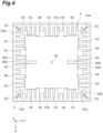
FIG. 4 is a plan view of a film-shaped adhesive member according to a modification. - Hereinafter, embodiments of the present disclosure will be described in detail with reference to the drawings. In the drawings, the same or corresponding parts are denoted by the same reference signs, and redundant description will be omitted.
- As illustrated in
FIG. 1 , aradiation detector 10 includes alight detection device 1, ascintillator layer 11, a plurality ofintegrated circuit devices 12, a flexibleprinted circuit substrate 13, and aheat sink 14. In theradiation detector 10, when radiation (for example, γ-rays, X-rays, and the like) enters thescintillator layer 11, scintillation light is generated in thescintillator layer 11, and the scintillation light is detected by thelight detection device 1. Theradiation detector 10 is used as a radiation imaging device, for example, in a medical radiological imaging apparatus, a nondestructive inspection apparatus, or the like. - The
light detection device 1 includes awiring substrate 2, alight receiving element 3, a film-shapedadhesive member 4, a plurality offirst connection members 6a, a plurality ofsecond connection members 6b (seeFIGS. 2 and3 ), and aprotection member 7. Thewiring substrate 2 has a front surface 2a and aback surface 2b. The light receivingelement 3 has afront surface 3a and aback surface 3b. The light receivingelement 3 is mounted on the front surface 2a of thewiring substrate 2 with theback surface 3b of the light receivingelement 3 facing the front surface 2a of thewiring substrate 2. Thelight receiving element 3 is a backside incidence type area sensor including a plurality of photodiodes (photoelectric conversion regions) arranged two-dimensionally. Hereinafter, the first direction in which a wiring substrate and a light receiving element are arranged is referred to as a Z direction, the second direction perpendicular to the first direction is referred to as an X direction, and the third direction perpendicular to the first direction and the second direction is referred to as a Y direction. - The plurality of
connection members wiring substrate 2 and thelight receiving element 3. Specifically, the plurality ofconnection members wiring substrate 2 and the plurality of electrodes provided on thelight receiving element 3. In the present embodiment, each of theconnection members adhesive member 4 bonds thewiring substrate 2 and thelight receiving element 3. In the present embodiment, the film-shapedadhesive member 4 is an anisotropic conductive film (ACF). The thickness of the film-shapedadhesive member 4 is, for example, 0.03 to 0.08 mm. Theprotection member 7 extends along the outer edge of the region between thewiring substrate 2 and thelight receiving element 3. In the present embodiment, theprotection member 7 surrounds the outer edge of the region between thewiring substrate 2 and thelight receiving element 3 in a frame shape. Theprotection member 7 is formed of, for example, an underfill resin agent. - The
scintillator layer 11 is disposed on thefront surface 3a of thelight receiving element 3. Thescintillator layer 11 is optically separated for each photodiode included in thelight receiving element 3 when viewed from the Z direction. The material of thescintillator layer 11 is, for example, LYSO or the like in a case where a γ-ray is to be detected, and is, for example, CsI, GOS, or the like in a case where an X-ray is to be detected. - The plurality of
integrated circuit devices 12 is mounted on theback surface 2b of thewiring substrate 2. Eachintegrated circuit device 12 is electrically and physically connected to thewiring substrate 2 by the plurality ofbump electrodes 12a. The flexible printedcircuit substrate 13 is electrically and physically connected to thewiring substrate 2 by the plurality ofbump electrodes 13a. In theradiation detector 10, the operation of thelight receiving element 3 is controlled by the plurality ofintegrated circuit devices 12, and the external input of the electric signal and the external output of the electric signal are performed by the flexible printedcircuit substrate 13. Theheat sink 14 is attached to theback surface 2b of thewiring substrate 2 in a state of being in contact with the plurality ofintegrated circuit devices 12. Theheat sink 14 cools eachintegrated circuit device 12. - As illustrated in
FIG. 2 , thelight receiving element 3 includes an n-type semiconductor substrate 30 made of silicon. The thickness of the n-type semiconductor substrate 30 is, for example, 30 to 300 µm. The impurity concentration of the n-type semiconductor substrate 30 is, for example, 1 × 10¹² to 1 × 10¹⁵/cm3. - A plurality of p-
type regions 31 is formed in a portion of the n-type semiconductor substrate 30 along theback surface 3b. The plurality of p-type regions 31 is two-dimensionally arranged with the X direction and the Y direction as a column direction and a row direction. The plurality of p-type regions 31 forms a plurality of pn junction regions with the n-type semiconductor substrate 30. In thelight receiving element 3, the plurality of pn junction regions functions as a plurality of photodiodes. The width of each p-type region 31 in the Z direction is, for example, 0.05 to 20 µm. The impurity concentration of each p-type region 31 is, for example, 1 × 10¹³ to 1 × 10²⁰/cm3. - A plurality of high-concentration n-
type regions 32 is formed in a portion of the n-type semiconductor substrate 30 along theback surface 3b. Each of the high-concentration n-type region 32 extends in a frame shape so as to surround each of the p-type region 31 when viewed from the Z direction. The plurality of high-concentration n-type regions 32 electrically isolates the plurality of photodiodes from each other, thereby suppressing occurrence of crosstalk between adjacent photodiodes. The width of each high-concentration n-type region 32 in the Z direction is, for example, 0.1 to several tens of µm. The impurity concentration of each high-concentration n-type region 32 is, for example, 1 × 10¹³ to 1 × 10²⁰/cm3. - A p-
type region 33 is formed in a portion of the n-type semiconductor substrate 30 along theback surface 3b. The p-type region 33 extends in a lattice shape so as to pass between the adjacent high-concentration n-type regions 32 when viewed from the Z direction. The p-type region 33 forms a pn junction region with the n-type semiconductor substrate 30. The width of the p-type region 33 in the Z direction is, for example, 0.05 to 20 µm. The impurity concentration of the p-type region 33 is, for example, 1 × 10¹³ to 1 × 10²⁰/cm3. - A plurality of
first connection members 6a is formed on theback surface 3b of thelight receiving element 3. Eachfirst connection member 6a is formed on each anode electrode (not illustrated) electrically connected to each of the p-type region 31. Each of the anode electrode is formed on the back surface of the n-type semiconductor substrate 30 and is located on each of the p-type region 31. When light enters each photodiode from thefront surface 3a side, a carrier is generated in each photodiode, and a photocurrent generated by the generation of the carrier is output to thewiring substrate 2 via each of thefirst connection member 6a. - A plurality of
second connection members 6b is formed on theback surface 3b of thelight receiving element 3. Each of thesecond connection member 6b is formed on each anode electrode (not illustrated) electrically connected to the plurality of high-concentration n-type regions 32 and p-type regions 33. The cathode electrode is formed on the back surface of the n-type semiconductor substrate 30, and extends in a lattice shape so as to cover the plurality of high-concentration n-type regions 32 and p-type regions 33. The plurality ofsecond connection members 6b is formed on a plurality of intersections of the cathode electrodes extending in a lattice shape. However, the plurality ofsecond connection members 6b is not formed on all the intersections, but is formed on the plurality of intersections for every predetermined number of intersections in both the X direction and the Y direction (seeFIG. 3 ). Each of thesecond connection members 6b is electrically connected to the ground potential via thewiring substrate 2. - As illustrated in
FIG. 3 , the film-shapedadhesive member 4 is disposed in the mountingregion 5 when viewed from the Z direction. The mountingregion 5 is a region where thewiring substrate 2 overlaps thelight receiving element 3 when viewed from the Z direction. In the present embodiment, the mountingregion 5 is a region where theback surface 3b of the light receiving element 3 (specifically, the back surface of the n-type semiconductor substrate 30) overlaps the front surface 2a of the wiring substrate 2(that is, the mounting surface of the wiring substrate 2) when viewed from the Z direction. In the present embodiment, when viewed from the Z direction, the outer edge of the film-shapedadhesive member 4 is located inside the outer edge of thelight receiving element 3. The mountingregion 5 has a pair offirst sides second sides first sides second sides second sides first sides first sides second sides region 5 has a rectangular shape with the pair offirst sides second sides wiring substrate 2 and thelight receiving element 3 also have substantially the same rectangular shape as the mountingregion 5 when viewed from the Z direction. InFIG. 3 , thelight receiving element 3 is indicated by a two-dot chain line, and theprotection member 7 is not illustrated. - The film-shaped
adhesive member 4 includes amain body portion 40. Themain body portion 40 has a pair offirst edges second edges first edge 41a extends on thefirst side 51a toward acenter 50 of the mountingregion 5 so as to notch the mountingregion 5. That is, thefirst edge 41a is located inside with respect to thefirst side 51a. Thefirst edge 41b extends on thefirst side 51b toward thecenter 50 of the mountingregion 5 so as to notch the mountingregion 5. That is, thefirst edge 41b is located inside with respect to thefirst side 51b. Thesecond edge 42a extends on thesecond side 52a toward thecenter 50 of the mountingregion 5 so as to notch the mountingregion 5. That is, thesecond edge 42a is located inside with respect to thesecond side 52a. Thesecond edge 42b extends on thesecond side 52b toward thecenter 50 of the mountingregion 5 so as to notch the mountingregion 5. That is, thesecond edge 42b is located inside with respect to thesecond side 52b. In the present embodiment, each of theedges center 50 of the mountingregion 5. Themain body portion 40 extends to each of the fourcorner portions 53 of the mountingregion 5. In other words, themain body portion 40 is not notched at each of the fourcorner portions 53 of the mountingregion 5. - The film-shaped
adhesive member 4 further includes a plurality of first projecting portions (projecting portions) 43 and a plurality of second projecting portions (projecting portions) 44. The plurality of projectingportions main body portion 40. The second projectingportion 44 has a width larger than the width of the first projectingportion 43. The width of the first projectingportion 43 is the width of the first projectingportion 43 in a direction perpendicular to the direction in which the first projectingportion 43 extends when viewed from the Z direction. The width of the second projectingportion 44 is the width of the second projectingportion 44 in a direction perpendicular to the direction in which the second projectingportion 44 extends when viewed from the Z direction. The width of the first projectingportion 43 is, for example, 0.5 to 2 mm. The width of the second projectingportion 44 is, for example, 1.5 to 6 mm. A slit opening to the side opposite to themain body portion 40 is formed at a distal end portion (end portion on the side opposite to the main body portion 40) of each of the second projectingportions 44. Note that the slit that opens to the side opposite to themain body portion 40 does not need to be formed at the distal end portion of each of the second projectingportions 44. - From the
first edge 41a of themain body portion 40, the plurality of projectingportions center 50 of the mountingregion 5. From thefirst edge 41b of themain body portion 40, the plurality of projectingportions center 50 of the mountingregion 5. In each of thefirst edges portions portions 43 is positioned between the adjacent second projectingportions 44. The predetermined interval is, for example, 0.5 to 2 mm. - The length of each of the projecting
portions first edge 41a (the length of each of the projectingportions first edge 41a. The length of each of the projectingportions first edge 41a. The length of each of the projectingportions first edge 41b (the length of each of the projectingportions first edge 41b. The length of each of the projectingportions first edge 41b. As described above, each of the plurality of projectingportions center 50 of the mountingregion 5 at the center of each of thefirst edges portions portions center 50 of the mountingregion 5 on both sides of the center of each of thefirst edges portions - From the
second edge 42a of themain body portion 40, the plurality of projectingportions center 50 of the mountingregion 5. From thesecond edge 42b of themain body portion 40, the plurality of projectingportions center 50 of the mountingregion 5. In each of thesecond edges portions portions 43 is positioned between the adjacent second projectingportions 44. The predetermined interval is, for example, 0.5 to 2 mm. - The length of each of the projecting
portions second edge 42a (the length of each of the projectingportions second edge 42a. The length of each of the projectingportions second edge 42a. The length of each of the projectingportions second edge 42b (the length of each of the projectingportions second edge 42b. The length of each of the projectingportions second edge 42b. As described above, each of the plurality of projectingportions center 50 of the mountingregion 5 at the center of each of thesecond edges portions portions center 50 of the mountingregion 5 on both sides of the center of each of thesecond edges portions - A pair of
slits main body portion 40. Theslit 40a extends from thesecond edge 42a toward thecenter 50 of the mountingregion 5. In the present embodiment, theslit 40a extends along the Y direction from the center of thesecond edge 42a. As an example, the width of theslit 40a in the X direction is equal to a predetermined interval between the projectingportions second edge 42a, and the length of theslit 40a in the Y direction is longer than the length of each of the projectingportions second edge 42a. Theslit 40b extends from thesecond edge 42b toward thecenter 50 of the mountingregion 5. In the present embodiment, theslit 40b extends along the Y direction from the center of thesecond edge 42b. As an example, the width of theslit 40b in the X direction is equal to a predetermined interval between the projectingportions second edge 42b, and the length of theslit 40b in the Y direction is longer than the length of each of the projectingportions second edge 42b. In the present embodiment, the film-shapedadhesive member 4 has a point-symmetrical shape with thecenter 50 of the mountingregion 5 as a center of symmetry when viewed from the Z direction. - The
main body portion 40 and the plurality of projectingportions connection members first connection members 6a overlaps themain body portion 40, the first projectingportion 43, or the second projectingportion 44 when viewed from the Z direction. Each of thesecond connection members 6b overlaps themain body portion 40 or the second projectingportion 44 when viewed from the Z direction. As described above, the film-shapedadhesive member 4 is an anisotropic conductive film. The anisotropic conductive film includes an insulating resin layer functioning as an adhesive layer, and a plurality of conductive particles dispersed in the insulating resin layer. Therefore, conductive particles are brought into contact with each other only in a portion of the film-shapedadhesive member 4 pressed by each of theconnection members connection members FIG. 3 , each of thefirst connection members 6a is indicated by dots whose color is white, and each of thesecond connection members 6b is indicated by dots whose color is black. - A method for manufacturing the
light detection device 1 will be described. First, thewiring substrate 2, thelight receiving element 3 in which the plurality ofconnection members back surface 3b, and the film-shapedadhesive member 4 in which the separator is attached to one front surface are prepared. The plurality ofconnection members light receiving element 3. Subsequently, the film-shapedadhesive member 4 is attached to the front surface 2a of thewiring substrate 2 in a state where the separator is attached to one front surface of the film-shapedadhesive member 4. Subsequently, the separator is peeled off from the film-shapedadhesive member 4. - Subsequently, the
light receiving element 3 is disposed on thewiring substrate 2 via the film-shapedadhesive member 4 such that the plurality ofconnection members back surface 3b of thelight receiving element 3 are positioned on the plurality of pads provided on thewiring substrate 2. Subsequently, thelight receiving element 3 is pressed against thewiring substrate 2 at a predetermined heating temperature. As a result, the plurality of pads provided on thewiring substrate 2 and the plurality of electrodes provided on thelight receiving element 3 are electrically and physically connected by the plurality ofconnection members wiring substrate 2 and thelight receiving element 3 are bonded by the film-shapedadhesive member 4. Subsequently, an underfill resin agent is applied along the outer edge of the region between thewiring substrate 2 and thelight receiving element 3 to form theprotection member 7. As described above, thelight detection device 1 is obtained. - The plurality of
connection members wiring substrate 2 when thewiring substrate 2, thelight receiving element 3, and the film-shapedadhesive member 4 are prepared. Alternatively, when thewiring substrate 2, thelight receiving element 3, and the film-shapedadhesive member 4 are prepared, a part of each of theconnection members wiring substrate 2, and the rest of each of theconnection members back surface 3b of thelight receiving element 3. Further, the film-shapedadhesive member 4 may be attached to theback surface 3b of thelight receiving element 3 in a state where the separator is attached to one front surface of the film-shapedadhesive member 4. - In the
light detection device 1, the film-shapedadhesive member 4 disposed in the mountingregion 5 includes amain body portion 40 having a shape notched on each of thesides region 5. This makes it less likely for the film-shapedadhesive member 4 to project from the mountingregion 5 at the time of bonding thewiring substrate 2 and thelight receiving element 3. Further, themain body portion 40 of the film-shapedadhesive member 4 extends to eachcorner portion 53 of the mountingregion 5, and the film-shapedadhesive member 4 disposed in the mountingregion 5 includes a plurality of projectingportions edges main body portion 40. As a result, the interval between thewiring substrate 2 and thelight receiving element 3 is easily kept constant at the time of bonding thewiring substrate 2 and thelight receiving element 3, and as a result, thewiring substrate 2 and thelight receiving element 3 are firmly bonded. Even if one of thewiring substrate 2 and thelight receiving element 3 is inclined with respect to the other at the time of bonding thewiring substrate 2 and thelight receiving element 3, and the pressure required for bonding becomes uneven, thewiring substrate 2 and thelight receiving element 3 are firmly bonded. Therefore, according to thelight detection device 1, it is possible to realize stable bonding between thewiring substrate 2 and thelight receiving element 3 while preventing projection of the film-shapedadhesive member 4. - In the
light detection device 1, each of theedges main body portion 40 extends along a curve recessed toward thecenter 50 of the mountingregion 5. At the time of bonding thewiring substrate 2 and thelight receiving element 3, the film-shapedadhesive member 4 easily projects at the center of each of thesides region 5, but according to the above-described configuration, projection of the film-shapedadhesive member 4 at the center of each of thesides region 5 can be more reliably prevented. - In the
light detection device 1, the second projectingportion 44 has a width larger than the width of the first projectingportion 43 at each of theedges main body portion 40. As a result, when a separator is peeled off from the film-shapedadhesive member 4 at the time of bonding thewiring substrate 2 and thelight receiving element 3, the defect of each of the projectingportions wiring substrate 2 and thelight receiving element 3 can be realized. In addition, since the defect of each of the projectingportions - In the
light detection device 1, each of the plurality of projectingportions center 50 of the mountingregion 5 at the center of each of theedges main body portion 40 has a length longer than the length of each of the plurality of projectingportions center 50 of the mountingregion 5 on both sides of the center of each of theedges main body portion 40. At the time of bonding thewiring substrate 2 and thelight receiving element 3, the film-shapedadhesive member 4 easily projects at the center of each of thesides region 5, but according to the above-described configuration, since the retraction amount of each of theedges main body portion 40 increases at the center of each of thesides region 5, projection of the film-shapedadhesive member 4 at the center of each of thesides region 5 can be more reliably prevented. Furthermore, when a separator is peeled off from the film-shapedadhesive member 4 at the time of bonding thewiring substrate 2 and thelight receiving element 3, the defect of each of the projectingportions 43 44 is suppressed so that stable bonding between thewiring substrate 2 and thelight receiving element 3 can be realized. In addition, since the defect of each of the projectingportions - In the
light detection device 1, the plurality ofconnection members light receiving element 3, it is possible to realize stable bonding between thewiring substrate 2 and thelight receiving element 3 while preventing projection of the film-shapedadhesive member 4. - In the
light detection device 1, themain body portion 40 and the plurality of projectingportions connection members connection members adhesive member 4, electrical connection between thewiring substrate 2 and thelight receiving element 3 by each of theconnection members - In the
light detection device 1, when viewed from the Z direction, the outer edge of the film-shapedadhesive member 4 is located inside the outer edge of thelight receiving element 3. As a result, projection of the film-shapedadhesive member 4 can be more reliably prevented. - In the
light detection device 1, the distance between the pair ofsecond sides first sides light receiving element 3, it is possible to realize stable bonding between thewiring substrate 2 and thelight receiving element 3 while preventing projection of the film-shapedadhesive member 4. - In the
light detection device 1, each of theslits main body portion 40 so as to extend from each of thesecond edges center 50 of the mountingregion 5 at the pair ofsecond edges first edges slits adhesive member 4 at each of thesecond sides region 5 can be more reliably prevented. In addition, while sufficiently securing the length of each of theslits adhesive member 4 at the time of bonding thewiring substrate 2 and thelight receiving element 3, the defect of themain body portion 40 is suppressed. Therefore, stable bonding between thewiring substrate 2 and thelight receiving element 3 can be realized. - In the
light detection device 1, the film-shapedadhesive member 4 is an anisotropic conductive film. As a result, electrical connection between thewiring substrate 2 and thelight receiving element 3 by each of theconnection members - In the
light detection device 1, theprotection member 7 extends along the outer edge of the region between thewiring substrate 2 and thelight receiving element 3. As a result, it is possible to suppress the occurrence of damage such as a defect in thelight receiving element 3. - The present disclosure is not limited to the above embodiments. For example, it is sufficient if the film-shaped
adhesive member 4 only includes at least one projecting portion (for example, the first projectingportion 43 or the second projecting portion 44) extending from at least one edge of each of theedges main body portion 40 to the side opposite to thecenter 50 of the mountingregion 5. Also in this case, as compared with the case where the film-shapedadhesive member 4 does not include at least one projecting portion, it is possible to realize stable bonding between thewiring substrate 2 and thelight receiving element 3 while preventing projection of the film-shapedadhesive member 4 for the same reason as in the above-described embodiment. As an example, at least one projecting portion may extend from each of theedges main body portion 40 to the side opposite to thecenter 50 of the mountingregion 5. - In the film-shaped
adhesive member 4, each of theedges main body portion 40 does not need to extend along a curve recessed toward thecenter 50 of the mountingregion 5. For example, each of theedges main body portion 40 may extend along a polygonal line recessed toward thecenter 50 side of the mountingregion 5. In the film-shapedadhesive member 4, a plurality ofslits 40a extending from thesecond edge 42a toward thecenter 50 of the mountingregion 5 may be formed in themain body portion 40. Similarly, in the film-shapedadhesive member 4, a plurality ofslits 40b extending from thesecond edge 42b toward thecenter 50 of the mountingregion 5 may be formed in themain body portion 40. Alternatively, in the film-shapedadhesive member 4, neither theslit 40a nor theslit 40b may be formed in themain body portion 40. In addition, the film-shapedadhesive member 4 may be a non-conductive film (NCF). Also in this case, it is possible to realize stable bonding between thewiring substrate 2 and thelight receiving element 3 while preventing projection of the film-shapedadhesive member 4. - In the above-described embodiment, the film-shaped
adhesive member 4 is disposed in the mountingregion 5 when viewed from the Z direction, and the outer edge of the film-shapedadhesive member 4 is located inside the outer edge of the mountingregion 5. However, a part of the outer edge of the film-shapedadhesive member 4 may be in contact with the outer edge of the mountingregion 5. Further, a part of the outer edge of the film-shapedadhesive member 4 may be positioned outside the outer edge of the mountingregion 5. For example, when at least a part of the outer edge of at least one of thewiring substrate 2 and thelight receiving element 3 is located outside the outer edge of the mountingregion 5 when viewed from the Z direction, in this at least a part, a part of the outer edge of the film-shapedadhesive member 4 may be located outside the outer edge of the mountingregion 5. - When viewed from the Z direction, the outer edge of the
light receiving element 3 may be located inside the outer edge of thewiring substrate 2, may be located outside the outer edge of thewiring substrate 2, or may coincide with the outer edge of thewiring substrate 2. Furthermore, when viewed from the Z direction, the outer edge of theback surface 3b of thelight receiving element 3 may be located inside the outer edge of the front surface 2a of thewiring substrate 2, may be located outside the outer edge of the front surface 2a of thewiring substrate 2, or may coincide with the outer edge of the front surface 2a of thewiring substrate 2. - In the above-described embodiment, the length of each of the projecting
portions edges main body portion 40. However, if each of the plurality of projectingportions center 50 of the mountingregion 5 at the center of each of theedges main body portion 40 has a length longer than the length of each of the plurality of projectingportions center 50 of the mountingregion 5 on both sides of the center of each of theedges main body portion 40, for example, a projecting portion having a short length exists in the center of each of theedges main body portion 40. - As illustrated in
FIG. 4 , in the film-shapedadhesive member 4, the distance between the pair ofsecond sides first sides FIG. 4 , the mountingregion 5 has a square shape. - The
light receiving element 3 is not limited to a backside incidence type area sensor, and may be a sensor having a single photodiode. In this case, the number of theconnection members connection members -
- 1 Light detection device
- 2 Wiring substrate
- 3 Light receiving element
- 4 Film-shaped adhesive member
- 5 Mounting region
- 6a First connection member (connection member)
- 6b Second connection member (connection member)
- 40 Main body portion
- 40a, 40b Slit
- 41a, 41b First edge
- 42a, 42b Second edge
- 43 First projecting portion (projecting portion)
- 44 Second projecting portion (projecting portion)
- 50 Center
- 51a, 51b First side
- 52a, 52b Second side
Claims (13)
- A light detection device, comprising:a wiring substrate;a light receiving element mounted on the wiring substrate;a connection member electrically connecting the wiring substrate and the light receiving element; anda film-shaped adhesive member bonding the wiring substrate and the light receiving element, whereina mounting region where the wiring substrate and the light receiving element overlap when viewed from a first direction in which the wiring substrate and the light receiving element are arranged has a pair of first sides facing each other in a second direction perpendicular to the first direction and a pair of second sides facing each other in a third direction perpendicular to the first direction and the second direction,the film-shaped adhesive member is disposed in the mounting region when viewed from the first direction, andthe film-shaped adhesive member includes:a main body portion having a pair of first edges extending so as to notch the mounting region on a center side of the mounting region in each of the pair of first sides and a pair of second edges extending so as to notch the mounting region on the center side of the mounting region in each of the pair of second sides; andat least one projecting portion extending from at least one edge of each of the pair of first edges and at least one edge of each of the pair of second edges to a side opposite to a center of the mounting region.
- The light detection device according to claim 1, wherein the at least one projecting portion extends from each of the pair of first edges and each of the pair of second edges to the side opposite to the center of the mounting region.
- The light detection device according to claim 1 or 2, wherein each of the pair of first edges and each of the pair of second edges extends along a curve recessed toward the center side of the mounting region.
- The light detection device according to any one of claims 1 to 3, wherein the film-shaped adhesive member includes a plurality of projecting portions as the at least one projecting portion, the plurality of projecting portions extending from each of the pair of first edges and each of the pair of second edges to the side opposite to the center of the mounting region.
- The light detection device according to claim 4, wherein
the plurality of projecting portions includes:a first projecting portion; anda second projecting portion having a width larger than a width of the first projecting portion. - The light detection device according to claim 4 or 5, wherein
the plurality of projecting portions includes:a plurality of third projecting portions extending to the side opposite to the center of the mounting region at a center of each of the pair of first edges and each of the pair of second edges; anda plurality of fourth projecting portions extending to the side opposite to the center of the mounting region on both sides of the center of each of the pair of first edges and each of the pair of second edges, andeach of the third projecting portions has a length longer than a length of each of the fourth projecting portions. - The light detection device according to any one of claims 1 to 6, wherein the connection member is each of a plurality of connection members arranged two-dimensionally.
- The light detection device according to claim 7, wherein the main body portion and the at least one projecting portion overlap the plurality of connection members when viewed from the first direction.
- The light detection device according to any one of claims 1 to 8, wherein an outer edge of the film-shaped adhesive member is located inside an outer edge of the light receiving element when viewed from the first direction.
- The light detection device according to any one of claims 1 to 9, wherein a distance between the pair of second sides is larger than a distance between the pair of first sides.
- The light detection device according to claim 10, wherein at least one slit extending from each of the pair of second edges to the center side of the mounting region is formed in the main body portion.
- The light detection device according to any one of claims 1 to 11, wherein the film-shaped adhesive member is an anisotropic conductive film.
- The light detection device according to any one of claims 1 to 12, further comprising a protection member extending along an outer edge of a region between the wiring substrate and the light receiving element.
Applications Claiming Priority (2)
| Application Number | Priority Date | Filing Date | Title |
|---|---|---|---|
| JP2022069985A JP7813645B2 (en) | 2022-04-21 | 2022-04-21 | Photodetector |
| PCT/JP2023/014532 WO2023204079A1 (en) | 2022-04-21 | 2023-04-10 | Light detection device |
Publications (2)
| Publication Number | Publication Date |
|---|---|
| EP4510191A1 true EP4510191A1 (en) | 2025-02-19 |
| EP4510191A4 EP4510191A4 (en) | 2025-11-26 |
Family
ID=88420021
Family Applications (1)
| Application Number | Title | Priority Date | Filing Date |
|---|---|---|---|
| EP23791728.1A Pending EP4510191A4 (en) | 2022-04-21 | 2023-04-10 | LIGHT DETECTION DEVICE |
Country Status (6)
| Country | Link |
|---|---|
| US (1) | US20250258306A1 (en) |
| EP (1) | EP4510191A4 (en) |
| JP (1) | JP7813645B2 (en) |
| CN (1) | CN119054080A (en) |
| IL (1) | IL316119A (en) |
| WO (1) | WO2023204079A1 (en) |
Family Cites Families (8)
| Publication number | Priority date | Publication date | Assignee | Title |
|---|---|---|---|---|
| JP3518404B2 (en) | 1999-03-31 | 2004-04-12 | 松下電器産業株式会社 | Paste application method |
| JP2005072978A (en) * | 2003-08-25 | 2005-03-17 | Renesas Technology Corp | Solid-state imaging device and manufacturing method thereof |
| JP4133429B2 (en) * | 2003-02-24 | 2008-08-13 | 浜松ホトニクス株式会社 | Semiconductor device |
| JP2007009022A (en) * | 2005-06-29 | 2007-01-18 | Sekisui Chem Co Ltd | Sheet adhesive, electronic component device manufacturing method, and electronic component device |
| JP5832852B2 (en) * | 2011-10-21 | 2015-12-16 | 浜松ホトニクス株式会社 | Photodetector |
| JP6038733B2 (en) | 2013-06-18 | 2016-12-07 | 浜松ホトニクス株式会社 | Manufacturing method of radiation detection unit |
| WO2019058429A1 (en) | 2017-09-19 | 2019-03-28 | 日立化成株式会社 | Adhesive film for semiconductor device manufacture and manufacturing method thereof |
| KR20200133072A (en) | 2019-05-16 | 2020-11-26 | 삼성전자주식회사 | Image Sensor Package |
-
2022
- 2022-04-21 JP JP2022069985A patent/JP7813645B2/en active Active
-
2023
- 2023-04-10 WO PCT/JP2023/014532 patent/WO2023204079A1/en not_active Ceased
- 2023-04-10 CN CN202380035010.6A patent/CN119054080A/en active Pending
- 2023-04-10 IL IL316119A patent/IL316119A/en unknown
- 2023-04-10 US US18/857,272 patent/US20250258306A1/en active Pending
- 2023-04-10 EP EP23791728.1A patent/EP4510191A4/en active Pending
Also Published As
| Publication number | Publication date |
|---|---|
| EP4510191A4 (en) | 2025-11-26 |
| JP7813645B2 (en) | 2026-02-13 |
| US20250258306A1 (en) | 2025-08-14 |
| WO2023204079A1 (en) | 2023-10-26 |
| JP2023160001A (en) | 2023-11-02 |
| CN119054080A (en) | 2024-11-29 |
| IL316119A (en) | 2024-12-01 |
Similar Documents
| Publication | Publication Date | Title |
|---|---|---|
| US9306108B2 (en) | Radiation detector | |
| US7649178B2 (en) | Solid state detector packaging technique | |
| EP1677353B1 (en) | Semiconductor photodetecting element and radiation detector | |
| JP6251683B2 (en) | Radiation detection apparatus, radiation detection method, and imaging system | |
| US11474050B2 (en) | Radiation detector module with insulating shield | |
| JP2004536313A (en) | Solid-state X-ray radiation detector module, mosaic structure thereof, imaging method, and imaging apparatus using the same | |
| US20240248218A1 (en) | X-ray detector component, x-ray detection module, imaging device and method for manufacturing an x-ray detector component | |
| JP4482253B2 (en) | Photodiode array, solid-state imaging device, and radiation detector | |
| NL2009365C2 (en) | Anode-illuminated radiation detector. | |
| JP3309618B2 (en) | X-ray CT system | |
| US20140367578A1 (en) | X-ray image sensor | |
| CN100466273C (en) | Photodiode array, manufacturing method thereof, and radiation detector | |
| US20250258306A1 (en) | Light detection device | |
| CN113474899B (en) | Method for manufacturing light detection device, and light detection device | |
| CN113169194B (en) | Image sensor, image sensor device, and computer tomography equipment | |
| JP2007155564A (en) | Radiation detector and radiation image detector | |
| JP3860758B2 (en) | Radiation detector | |
| EP4078243B1 (en) | Photon counting detector | |
| EP4585973A1 (en) | X-ray detector | |
| US20260130005A1 (en) | Light detection element | |
| US20250020814A1 (en) | Scintillator crystal and photomultiplier assemblies with improved emission detection |
Legal Events
| Date | Code | Title | Description |
|---|---|---|---|
| STAA | Information on the status of an ep patent application or granted ep patent |
Free format text: STATUS: THE INTERNATIONAL PUBLICATION HAS BEEN MADE |
|
| PUAI | Public reference made under article 153(3) epc to a published international application that has entered the european phase |
Free format text: ORIGINAL CODE: 0009012 |
|
| STAA | Information on the status of an ep patent application or granted ep patent |
Free format text: STATUS: REQUEST FOR EXAMINATION WAS MADE |
|
| 17P | Request for examination filed |
Effective date: 20241113 |
|
| AK | Designated contracting states |
Kind code of ref document: A1 Designated state(s): AL AT BE BG CH CY CZ DE DK EE ES FI FR GB GR HR HU IE IS IT LI LT LU LV MC ME MK MT NL NO PL PT RO RS SE SI SK SM TR |
|
| DAV | Request for validation of the european patent (deleted) | ||
| DAX | Request for extension of the european patent (deleted) | ||
| REG | Reference to a national code |
Ref country code: DE Ref legal event code: R079 Free format text: PREVIOUS MAIN CLASS: H01L0027146000 Ipc: H10F0039180000 |
|
| A4 | Supplementary search report drawn up and despatched |
Effective date: 20251028 |
|
| RIC1 | Information provided on ipc code assigned before grant |
Ipc: H10F 39/18 20250101AFI20251022BHEP Ipc: H10F 39/00 20250101ALI20251022BHEP Ipc: H10F 77/00 20250101ALI20251022BHEP |
|
| GRAP | Despatch of communication of intention to grant a patent |
Free format text: ORIGINAL CODE: EPIDOSNIGR1 |
|
| STAA | Information on the status of an ep patent application or granted ep patent |
Free format text: STATUS: GRANT OF PATENT IS INTENDED |
|
| INTG | Intention to grant announced |
Effective date: 20260713 |
|
| RIN1 | Information on inventor provided before grant (corrected) |
Inventor name: SUZUKI, TAKAHARU Inventor name: SUWA, YOSUKE Inventor name: NAGURA, KEISUKE |