EP4510185A1 - Power overlay structure for a multi-chip semiconductor package - Google Patents
Power overlay structure for a multi-chip semiconductor package Download PDFInfo
- Publication number
- EP4510185A1 EP4510185A1 EP24193418.1A EP24193418A EP4510185A1 EP 4510185 A1 EP4510185 A1 EP 4510185A1 EP 24193418 A EP24193418 A EP 24193418A EP 4510185 A1 EP4510185 A1 EP 4510185A1
- Authority
- EP
- European Patent Office
- Prior art keywords
- gate
- pad
- interconnect layer
- package
- common
- Prior art date
- Legal status (The legal status is an assumption and is not a legal conclusion. Google has not performed a legal analysis and makes no representation as to the accuracy of the status listed.)
- Pending
Links
Images









Classifications
-
- H—ELECTRICITY
- H10—SEMICONDUCTOR DEVICES; ELECTRIC SOLID-STATE DEVICES NOT OTHERWISE PROVIDED FOR
- H10W—GENERIC PACKAGES, INTERCONNECTIONS, CONNECTORS OR OTHER CONSTRUCTIONAL DETAILS OF DEVICES COVERED BY CLASS H10
- H10W70/00—Package substrates; Interposers; Redistribution layers [RDL]
- H10W70/60—Insulating or insulated package substrates; Interposers; Redistribution layers
- H10W70/611—Insulating or insulated package substrates; Interposers; Redistribution layers for connecting multiple chips together
-
- H—ELECTRICITY
- H10—SEMICONDUCTOR DEVICES; ELECTRIC SOLID-STATE DEVICES NOT OTHERWISE PROVIDED FOR
- H10W—GENERIC PACKAGES, INTERCONNECTIONS, CONNECTORS OR OTHER CONSTRUCTIONAL DETAILS OF DEVICES COVERED BY CLASS H10
- H10W70/00—Package substrates; Interposers; Redistribution layers [RDL]
- H10W70/60—Insulating or insulated package substrates; Interposers; Redistribution layers
-
- H—ELECTRICITY
- H10—SEMICONDUCTOR DEVICES; ELECTRIC SOLID-STATE DEVICES NOT OTHERWISE PROVIDED FOR
- H10W—GENERIC PACKAGES, INTERCONNECTIONS, CONNECTORS OR OTHER CONSTRUCTIONAL DETAILS OF DEVICES COVERED BY CLASS H10
- H10W20/00—Interconnections in chips, wafers or substrates
- H10W20/20—Interconnections within wafers or substrates, e.g. through-silicon vias [TSV]
-
- H—ELECTRICITY
- H10—SEMICONDUCTOR DEVICES; ELECTRIC SOLID-STATE DEVICES NOT OTHERWISE PROVIDED FOR
- H10W—GENERIC PACKAGES, INTERCONNECTIONS, CONNECTORS OR OTHER CONSTRUCTIONAL DETAILS OF DEVICES COVERED BY CLASS H10
- H10W70/00—Package substrates; Interposers; Redistribution layers [RDL]
- H10W70/01—Manufacture or treatment
- H10W70/05—Manufacture or treatment of insulating or insulated package substrates, or of interposers, or of redistribution layers
- H10W70/093—Connecting or disconnecting other interconnections thereto or therefrom, e.g. connecting bond wires or bumps
-
- H—ELECTRICITY
- H10—SEMICONDUCTOR DEVICES; ELECTRIC SOLID-STATE DEVICES NOT OTHERWISE PROVIDED FOR
- H10W—GENERIC PACKAGES, INTERCONNECTIONS, CONNECTORS OR OTHER CONSTRUCTIONAL DETAILS OF DEVICES COVERED BY CLASS H10
- H10W70/00—Package substrates; Interposers; Redistribution layers [RDL]
- H10W70/40—Leadframes
- H10W70/411—Chip-supporting parts, e.g. die pads
-
- H—ELECTRICITY
- H10—SEMICONDUCTOR DEVICES; ELECTRIC SOLID-STATE DEVICES NOT OTHERWISE PROVIDED FOR
- H10W—GENERIC PACKAGES, INTERCONNECTIONS, CONNECTORS OR OTHER CONSTRUCTIONAL DETAILS OF DEVICES COVERED BY CLASS H10
- H10W70/00—Package substrates; Interposers; Redistribution layers [RDL]
- H10W70/40—Leadframes
- H10W70/481—Leadframes for devices being provided for in groups H10D8/00 - H10D48/00
-
- H—ELECTRICITY
- H10—SEMICONDUCTOR DEVICES; ELECTRIC SOLID-STATE DEVICES NOT OTHERWISE PROVIDED FOR
- H10W—GENERIC PACKAGES, INTERCONNECTIONS, CONNECTORS OR OTHER CONSTRUCTIONAL DETAILS OF DEVICES COVERED BY CLASS H10
- H10W70/00—Package substrates; Interposers; Redistribution layers [RDL]
- H10W70/60—Insulating or insulated package substrates; Interposers; Redistribution layers
- H10W70/62—Insulating or insulated package substrates; Interposers; Redistribution layers characterised by their interconnections
- H10W70/63—Vias, e.g. via plugs
- H10W70/635—Through-vias
-
- H—ELECTRICITY
- H10—SEMICONDUCTOR DEVICES; ELECTRIC SOLID-STATE DEVICES NOT OTHERWISE PROVIDED FOR
- H10W—GENERIC PACKAGES, INTERCONNECTIONS, CONNECTORS OR OTHER CONSTRUCTIONAL DETAILS OF DEVICES COVERED BY CLASS H10
- H10W70/00—Package substrates; Interposers; Redistribution layers [RDL]
- H10W70/60—Insulating or insulated package substrates; Interposers; Redistribution layers
- H10W70/62—Insulating or insulated package substrates; Interposers; Redistribution layers characterised by their interconnections
- H10W70/65—Shapes or dispositions of interconnections
-
- H—ELECTRICITY
- H10—SEMICONDUCTOR DEVICES; ELECTRIC SOLID-STATE DEVICES NOT OTHERWISE PROVIDED FOR
- H10W—GENERIC PACKAGES, INTERCONNECTIONS, CONNECTORS OR OTHER CONSTRUCTIONAL DETAILS OF DEVICES COVERED BY CLASS H10
- H10W70/00—Package substrates; Interposers; Redistribution layers [RDL]
- H10W70/60—Insulating or insulated package substrates; Interposers; Redistribution layers
- H10W70/62—Insulating or insulated package substrates; Interposers; Redistribution layers characterised by their interconnections
- H10W70/65—Shapes or dispositions of interconnections
- H10W70/652—Cross-sectional shapes
-
- H—ELECTRICITY
- H10—SEMICONDUCTOR DEVICES; ELECTRIC SOLID-STATE DEVICES NOT OTHERWISE PROVIDED FOR
- H10W—GENERIC PACKAGES, INTERCONNECTIONS, CONNECTORS OR OTHER CONSTRUCTIONAL DETAILS OF DEVICES COVERED BY CLASS H10
- H10W70/00—Package substrates; Interposers; Redistribution layers [RDL]
- H10W70/60—Insulating or insulated package substrates; Interposers; Redistribution layers
- H10W70/62—Insulating or insulated package substrates; Interposers; Redistribution layers characterised by their interconnections
- H10W70/65—Shapes or dispositions of interconnections
- H10W70/658—Shapes or dispositions of interconnections for devices provided for in groups H10D8/00 - H10D48/00
-
- H—ELECTRICITY
- H10—SEMICONDUCTOR DEVICES; ELECTRIC SOLID-STATE DEVICES NOT OTHERWISE PROVIDED FOR
- H10W—GENERIC PACKAGES, INTERCONNECTIONS, CONNECTORS OR OTHER CONSTRUCTIONAL DETAILS OF DEVICES COVERED BY CLASS H10
- H10W70/00—Package substrates; Interposers; Redistribution layers [RDL]
- H10W70/60—Insulating or insulated package substrates; Interposers; Redistribution layers
- H10W70/67—Insulating or insulated package substrates; Interposers; Redistribution layers characterised by their insulating layers or insulating parts
- H10W70/68—Shapes or dispositions thereof
- H10W70/685—Shapes or dispositions thereof comprising multiple insulating layers
-
- H—ELECTRICITY
- H10—SEMICONDUCTOR DEVICES; ELECTRIC SOLID-STATE DEVICES NOT OTHERWISE PROVIDED FOR
- H10W—GENERIC PACKAGES, INTERCONNECTIONS, CONNECTORS OR OTHER CONSTRUCTIONAL DETAILS OF DEVICES COVERED BY CLASS H10
- H10W72/00—Interconnections or connectors in packages
- H10W72/071—Connecting or disconnecting
- H10W72/072—Connecting or disconnecting of bump connectors
-
- H—ELECTRICITY
- H10—SEMICONDUCTOR DEVICES; ELECTRIC SOLID-STATE DEVICES NOT OTHERWISE PROVIDED FOR
- H10W—GENERIC PACKAGES, INTERCONNECTIONS, CONNECTORS OR OTHER CONSTRUCTIONAL DETAILS OF DEVICES COVERED BY CLASS H10
- H10W72/00—Interconnections or connectors in packages
- H10W72/90—Bond pads, in general
-
- H—ELECTRICITY
- H10—SEMICONDUCTOR DEVICES; ELECTRIC SOLID-STATE DEVICES NOT OTHERWISE PROVIDED FOR
- H10W—GENERIC PACKAGES, INTERCONNECTIONS, CONNECTORS OR OTHER CONSTRUCTIONAL DETAILS OF DEVICES COVERED BY CLASS H10
- H10W72/00—Interconnections or connectors in packages
- H10W72/90—Bond pads, in general
- H10W72/941—Dispositions of bond pads
- H10W72/944—Dispositions of multiple bond pads
-
- H—ELECTRICITY
- H10—SEMICONDUCTOR DEVICES; ELECTRIC SOLID-STATE DEVICES NOT OTHERWISE PROVIDED FOR
- H10W—GENERIC PACKAGES, INTERCONNECTIONS, CONNECTORS OR OTHER CONSTRUCTIONAL DETAILS OF DEVICES COVERED BY CLASS H10
- H10W90/00—Package configurations
-
- H—ELECTRICITY
- H10—SEMICONDUCTOR DEVICES; ELECTRIC SOLID-STATE DEVICES NOT OTHERWISE PROVIDED FOR
- H10W—GENERIC PACKAGES, INTERCONNECTIONS, CONNECTORS OR OTHER CONSTRUCTIONAL DETAILS OF DEVICES COVERED BY CLASS H10
- H10W90/00—Package configurations
- H10W90/701—Package configurations characterised by the relative positions of pads or connectors relative to package parts
-
- H—ELECTRICITY
- H10—SEMICONDUCTOR DEVICES; ELECTRIC SOLID-STATE DEVICES NOT OTHERWISE PROVIDED FOR
- H10W—GENERIC PACKAGES, INTERCONNECTIONS, CONNECTORS OR OTHER CONSTRUCTIONAL DETAILS OF DEVICES COVERED BY CLASS H10
- H10W90/00—Package configurations
- H10W90/701—Package configurations characterised by the relative positions of pads or connectors relative to package parts
- H10W90/791—Package configurations characterised by the relative positions of pads or connectors relative to package parts of direct-bonded pads
-
- H—ELECTRICITY
- H10—SEMICONDUCTOR DEVICES; ELECTRIC SOLID-STATE DEVICES NOT OTHERWISE PROVIDED FOR
- H10W—GENERIC PACKAGES, INTERCONNECTIONS, CONNECTORS OR OTHER CONSTRUCTIONAL DETAILS OF DEVICES COVERED BY CLASS H10
- H10W90/00—Package configurations
- H10W90/701—Package configurations characterised by the relative positions of pads or connectors relative to package parts
- H10W90/721—Package configurations characterised by the relative positions of pads or connectors relative to package parts of bump connectors
- H10W90/724—Package configurations characterised by the relative positions of pads or connectors relative to package parts of bump connectors between a chip and a stacked insulating package substrate, interposer or RDL
Definitions
- the present disclosure relates generally to semiconductor packages, and more particularly to a multi-chip semiconductor package having an interconnecting power overlay structure.
- Power semiconductor devices such as switches and rectifiers, are key components of power electronic circuits (e.g., switched mode power supplies, inverters, rectifiers, and the like).
- High power applications typically require multi-chip assemblies comprising multiple power semiconductor devices connected together to carry large amounts of current and to support high voltages.
- a top surface of each power semiconductor device such as metal oxide semiconductor field effect transistor (MOSFET), includes a gate pad and at least one source pad which are electrically connected to gate and source pads of other devices in the multi-chip assembly.
- MOSFET metal oxide semiconductor field effect transistor
- the electrical connections of multiple gate pads and source pads are typically formed using wire bonds and complex routing configurations to a common gate pad and at least one common source pad.
- the common gate pad and at least one common source pad of the multi-chip semiconductor assembly may be connected to an external power electronic circuit such that the multi-chip semiconductor assembly operates as a singular power processing unit.
- An alternative to the wire bonding of gate pads and source pads may be the use of one or more planar interconnect layers separated by interconnect layers disposed over the top surfaces of the semiconductor devices.
- the interconnect layers may include metallization vias which extend through the interconnect layer to electrically couple the source pads and gate pads to the common gate pad and the common source pad disposed on upper interconnect layers of the multi-chip semiconductor assembly to deliver power to the semiconductor devices through the metallization vias.
- the common gate pad and the common source pad on an uppermost interconnect layer require sufficient surface area to solder, sinter, copper-bond, copper-clip, or otherwise connect the common gate pad and the source pad of the multi-chip assembly with the external power electronic circuitry.
- the available surface area of the common gate pad and the common source pad are generally limited by the overall surface area of the multi-chip semiconductor assembly. Further, direct soldering, sintering, copper-bonding, and copper-clipping onto smaller common gate pads and common source pads introduce bonding stresses onto the multi-chip semiconductor assembly and form less reliable interconnections.
- a device rated at 240A is significantly larger than a device rated for 60A. This will make the packaging and interconnection easier, however, the device yield will be significantly lower.
- a multi-chip semiconductor package in one aspect, includes an interconnect layer having an upper surface and a bottom surface, wherein the interconnect layer includes a dielectric material, at least one common source pad disposed on the upper surface of the interconnect layer, at least one common gate pad disposed on the upper surface of the interconnect layer, and a plurality of semiconductor devices each including a gate pad and at least one source pad adhered onto the interconnect layer, wherein the source pads of the plurality of semiconductor devices are electrically connected to the at least one common source pad, and wherein the source pads of the plurality of semiconductor devices are electrically connected in parallel with one another, and wherein the gate pads of the plurality of semiconductor devices are electrically connected to the common gate pad, and wherein the gate pads of the plurality of semiconductor devices are electrically connected in parallel with one another.
- a method of manufacturing a multi-chip semiconductor package includes forming at least one source via pathway and at least one gate via pathway through an interconnect layer, aligning at least one source pad and a gate pad of a plurality of semiconductor devices with the least one source via pathway and the at least one gate via pathway, respectively, and adhering the plurality of semiconductor devices to the interconnect layer, wherein a surface area of the interconnect layer is substantially equal to a surface area of a footprint defined by the plurality of semiconductor devices
- approximating language such as “generally,” “substantially,” and “about,” as used herein indicates that the term so modified may apply to only an approximate degree, as would be recognized by one of ordinary skill in the art, rather than to an absolute or perfect degree. Accordingly, a value modified by a term or terms, such as “about,” “approximately,” and “substantially,” is not to be limited to the precise value specified. In at least some instances, the approximating language may correspond to the precision of an instrument for measuring the value.
- range limitations may be identified. Such ranges may be combined and/or interchanged, and include all the sub-ranges contained therein unless context or language indicates otherwise.
- first ⁇ ⁇ ⁇ ⁇ ⁇ ⁇ ⁇ ⁇ ⁇ ⁇ ⁇ ⁇ ⁇ ⁇ ⁇ ⁇ ⁇ ⁇ ⁇ ⁇ ⁇ ⁇ ⁇ ⁇ ⁇ ⁇ ⁇ ⁇ ⁇ ⁇ ⁇ ⁇ ⁇ ⁇ ⁇ ⁇ ⁇ ⁇ ⁇ ⁇ ⁇ ⁇ ⁇ ⁇ ⁇ ⁇ ⁇ ⁇ ⁇ ⁇ ⁇ ⁇ ⁇ ⁇ ⁇ ⁇ ⁇ ⁇ ⁇ ⁇ ⁇ ⁇ ⁇ ⁇ ⁇ ⁇ ⁇ ⁇ ⁇ ⁇ ⁇ ⁇ ⁇ ⁇ ⁇ ⁇ ⁇ ⁇ ⁇ ⁇ ⁇ ⁇ ⁇ ⁇ ⁇ ⁇ ⁇ ⁇ ⁇ ⁇ ⁇ ⁇ ⁇ ⁇ ⁇ ⁇ ⁇ ⁇ ⁇ ⁇ ⁇ ⁇ ⁇ ⁇ ⁇ ⁇ ⁇ ⁇ ⁇ ⁇ ⁇ ⁇ ⁇ ⁇ ⁇ ⁇ ⁇ ⁇ ⁇ ⁇ ⁇ ⁇ ⁇ ⁇ ⁇ ⁇
- Embodiments of the disclosure relate generally to structures and methods for packaging multiple semiconductor devices and, more particularly to multi-chip semiconductor package having an interconnecting power overlay (POL) structure.
- the methods, systems, and apparatus described herein overcome at least some disadvantages of at least some known multi-chip semiconductor packages. More specifically, the systems and apparatus described herein provide a POL package configured as a redistribution layer (RDL) positioned directly over multiple semiconductor devices. Accordingly, the POL package is also referred to herein as a POL-RDL package.
- the POL-RDL package includes an oversized surface area relative to a footprint of the molding defined by the semiconductor devices (or more generally to a footprint of the semiconductor devices), which improves available surface area for placement of common gate pads, common source pads and overlayed contact pads. The oversized surface area also allows for placement of more complex configurations of common source pads, common gate pads and gate bridges, and additional interconnect layers and interconnect layers.
- a multi-chip semiconductor package includes least one interconnect layer having an upper surface and a bottom surface, at least one common source pad disposed on the upper surface of the at least one interconnect layer, at least one common gate pad disposed on the upper surface of the at least one interconnect layer and, a plurality of semiconductor devices.
- Each of the semiconductor devices have a gate pad and at least one source pad adhered onto a bottom surface of a first interconnect layer of the at least one interconnect layer.
- the bottom surface of the first interconnect layer has an adhesive layer.
- the source pads of the plurality of semiconductor devices are electrically connected to the at least one common source pad, and the source pads of the plurality of semiconductor devices are electrically connected in parallel with one another.
- the gate pads of the plurality of semiconductor devices are electrically connected to the at least one common gate pad, and the gate pads of the plurality of semiconductor devices are electrically connected in parallel with one another.
- routing refers to metallization vias disposed within via pathways of a interconnect layer and to trace connections, pads, contacts and contact pads disposed on the interconnect layer.
- the routing may also include surface-mount resistors, thin film resistors and associated pads for placement of surface-mount resistors post-fabrication.
- Additional interconnect layers and routing may be laminated or otherwise fabricated over a first interconnect layer to facilitate additional routing configurations.
- the terms “package gate pad” and “package source pad” refer to common gate pads and common source pads on an uppermost interconnect layer which are electrically connected to external power electronic circuitry. Any of the first interconnect layer and additional interconnect layers disclosed herein may be directly connected to external power electronic circuitry or may have additional interconnect layers and routing. Therefore, the terms “package gate pad,” “package source pad,” “common gate pads,” and “common source pads” are used interchangeably.
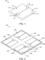
- FIG. 1 illustrates a perspective view of one embodiment of a semiconductor device 100.
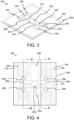
- FIG. 2 illustrates a perspective view of a molding 102 including at least two semiconductor devices 100 (also referred to as a plurality of semiconductor devices 100).
- the semiconductor device 100 includes a dielectric material 106 that defines an upper surface 101.
- the semiconductor device 100 further includes at least one source pad 110 and a gate pad 120 disposed on the upper surface 101 of the semiconductor device 100.
- the at least one source pad 110 includes a top contact surface 112.
- the gate pad 120 includes a top contact surface 122.
- the top contact surfaces 112, 122 of the gate pad 120 and each of the at least one source pad 110 are electrically isolated from each other by the dielectric material 106. In some embodiments, at least a portion of the gate pad 120 and the at least one source pad 110 at least partially extend below the upper surface 101. In some embodiments, the top contact surface 112 of the at least one source pad 110 and the top contact surface 122 of the gate pad 120 are flush with the surface of the dielectric material 106. In some embodiments, the top contact surface 112 of the at least one source pad 110 and the top contact surface 122 of the gate pad 120 are below the surface of the dielectric material 106. In some embodiments, the top contact surface 112 of the at least one source pad 110 and the top contact surface 122 of the gate pad 120 are above the surface of the dielectric material 106.
- the molding 102 includes a underfill material 103 that defines an upper surface 104, and a plurality of semiconductor devices 100 at least partially disposed in the molding 102 and surrounded by the underfill material 103.
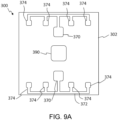
- the plurality of semiconductor devices 100 embedded in the molding 102 define a footprint 105 (as best shown in FIG. 4 ).
- FIGS. 3-8 illustrate one or more embodiments of a multi-chip semiconductor package 200.
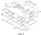
- FIG. 3 illustrates a perspective view of the multi-chip semiconductor package 200
- FIG. 4 illustrates a plan, partially transparent view of the semiconductor package 200
- FIGS. 5 and 6 illustrate exploded views of the semiconductor package 200.
- FIGS. 7 and 8 illustrate cross-sectional views of the semiconductor package 200 taken along lines A-A' and B-B' of FIG. 4 , respectively.
- the multi-chip semiconductor package 200 operates as a metal-oxide-semiconductor field-effect transistor (MOSFET) having two or more semiconductor devices 100.
- the multi-chip semiconductor package 200 includes a POL-RDL package 250 having at least one common source pad 280 and a gate bridge 290.
- the POL-RDL package 250 includes a first interconnect layer 260 and an adhesive layer 262 disposed over the molding 102 (as best shown in FIG. 5 ).
- the first interconnect layer 260 is in the form of a lamination or a film, and may be formed of one a plurality of dielectric materials, such as Kapton ® polyimide, Ultem ® polyetherimide, polytetrafluoroethylene (PTFE), Upilex ® , polysulfone materials (e.g., Udel ® polysulphone, Radel ® polyphenolsulphone), or another polymer film, such as a liquid crystal polymer (LCP), Bismaleimide-Triazine resin, Ajinomoto Build-up Film ® ABF or a polyimide material.
- the POL-RDL package 250 has a total thickness in the range of 25 microns to 300 microns.
- the POL-RDL package 250 (which may include any number of interconnect layers 260, trace connections, source and gate pads) is fully fabricated and positioned over the molding 102 (together with the plurality of semiconductor devices 100 embedded in the molding 102), and the first interconnect layer 260 is adhered to the source pads 110 and the gate pads 120 by the adhesive layer 262. That is, the adhesive layer 262 is positioned between the first interconnect layer 260 and the molding 102.
- the semiconductor devices 100 may be adhered directly onto the adhesive layer 262 without a molding. A molding or an underfill material may be deposited between the semiconductor devices 100 at a later stage.
- metallization vias are formed in source via pathways 264 and gate via pathways 266 extending through the first interconnect layer 260 (and in any number of additional interconnect layers as explained in further detail below with reference to FIGS. 9A - 14B ), associated metal interconnect structures and routing are built over the first interconnect layer 260 (and in any number of additional interconnect layers), and the adhesive layer 262 is applied to a bottom surface of the first interconnect layer 260.
- the semiconductor devices 100 (either as part of the molding 102 or individually) are aligned with the source via pathways 264 and gate via pathways 266 extending through the first interconnect layer 160 in accordance with one or more configurations, and the molding 102 is cured to form the multi-chip semiconductor package 200.
- any of the steps in fabrication may be performed in a different sequence.
- the source via pathways 264 and gate via pathways 266 may be filled prior to aligning and adhering the semiconductor devices 100 (either as part of the molding 102 or individually).
- the at least one common source pad 280 and the gate bridge 290 are formed on an upper surface 261 of the first interconnect layer 260.
- Source via pathways 264 and gate via pathways 266 extend through the first interconnect layer 260 and the adhesive layer 262.
- the POL-RDL package 250 of the multi-chip semiconductor package 200 also includes a metal interconnect structure 267 that extends through the source via pathways 264 and the gate via pathways 266.
- the metal interconnect structure 267 electrically couples the top contact surface 112 of each of the source pads 110 to the at least one common source pad 280 of the POL-RDL package 250, and likewise the metal interconnect structure 267 electrically couples the top contact surface 122 of the gate pad 120 to the gate bridge 290 of the POL-RDL package 250.
- the metal interconnect structure 267 is formed by filling the source via pathways 264 and the gate via pathways 266 with a conductive material (i.e., conductive epoxy, paste, or solder and the like).
- the vias have plated copper and a sputtered adhesion layer such as titanium or Ti-tungsten.
- the metal interconnect structure 267 is formed during deposition of the at least one common source pad 280 and the gate bridge 290. By way of example, as the at least one common source pad 280 and the gate bridge 290 are deposited, the source via pathways 264 and the gate via pathways 266 are also filled. Subsequently, the at least one common source pad 280 and the gate bridge 290 are electroplated or otherwise plated or fabricated to a desired thickness.
- the gate bridge 290 includes a common gate pad 292 and gate contacts 296 connected by trace connections 294. As best shown in FIG. 6 , each of the gate contacts 296 of the gate bridge 290 are aligned with the gate pads 120 of the plurality of semiconductor devices 100. As shown in FIGS. 7 and 8 , the common gate pad 292, the trace connection 294, and the gate contacts 296 are disposed on the first interconnect layer 260 of the POL-RDL package 250, and the gate contacts 296 are electrically connected to the gate pads 120 by the metal interconnect structure 267.
- the trace connection 294 extends from the common gate pad 292 to the gate contacts 296, and may have any number of branches and bends to establish the electrical connection between the common gate pad 292 and the gate contacts 296.
- the gate bridge 290 has an I-shape with each end being a pair of gate contacts 296 that align with gate pads 120 of the plurality of semiconductor devices 100, however as shown in FIGS. 11 through 13A , the gate bridge 290 can have other shapes and configurations but maintain equal path lengths, as explained in further detail below.
- the trace connections 294 of the gate bridge 290 have the same length between the common gate pad 292 and gate contacts 296 such that there are equal resistivity values between the common gate pad 292 and gate contacts 296.
- the length of the trace connections 294 impacts inductance.
- the common gate pad 292 and the length of the trace connections 294 can be made similar to all the gate pads 120 of the semiconductor devices 100.
- the POL-RDL package 250 provides for flexibility in optimizing the gate-source loop inductance depending on how it is oriented and connected to the next level circuit. For example, the resistivity and trance length of two of the semiconductor devices 100 to be different than the other two semiconductor devices 100 so that the eventual gate source loops to each device is similar/equal.
- the semiconductor devices 100 can be oriented or positioned on the adhesive layer 262 and the first interconnect layer 260 such that the gate pad 120 of each of the semiconductor devices are an equal length from the common gate pad 292 of the gate bridge 290.
- any one of the trace connections 294 may include a surface-mount resistor or a thin-film resistor to balance resistivity values.
- an outer peripheral edge 108 of the underfill material 103 defines a surface area of the molding 102.
- Each of the plurality of the semiconductor devices 100 are spaced from the outer peripheral edge 108 of the molding 102, and the placement of the plurality of the semiconductor devices 100 in the molding 102 defines a footprint 105 of the molding 102 (please note the footprint 105, as defined herein, generally has a smaller surface than the molding 102 itself).
- the plurality of the semiconductor devices 100 are directly adhered to the first interconnect layer 260 (and adhesive layer 262) without the use of the molding 102, and in such embodiments, the footprint 105 is defined as the placement of the plurality of semiconductor devices 100 on the bottom surface of the first interconnect layer 260.
- the footprint 105 is therefore defined as the outermost peripheral edges of the plurality of the semiconductor devices 100.
- the first interconnect layer 260 of the POL-RDL package 250 is generally placed over the entire molding 102 and has a surface area greater than the footprint 105 of the molding 102 such that an outer peripheral edge 268 of the first interconnect layer 260 extends beyond the footprint 105 of the molding 102 and the outermost peripheral edges of the plurality of semiconductor devices 100 (please note that the outer peripheral edge 268 does not extend beyond a perimeter of the molding itself 102).
- the adhesive layer 262 extends to the outer peripheral edge 268 of the first interconnect layer 260.
- the overhang region 274 of the POL-RDL package 250 increases available surface area of the first interconnect layer 260 for placement of a larger common source pad 280 and a larger common gate pad 292.
- the overhang region 274 also allows for placement of more complex configurations of common source pads 280, gate bridges 290, common gate pads 292 and trace connections for the common source pads 280 and common gate pads 292 as explained in further detail below.
- the POL-RDL package 250 thus facilitates improved routing and more robust connections of the at least one common source pad 280 and the common gate pad 292 to external power electronic circuitry or to additional interconnect layers disposed over the first interconnect layer 260 (as explained in further detail below).
- connection of external power electronic circuitry - either directly onto the at least one common source pad 280 and the common gate pad 292 or by the additional interconnect layers - enables the source pads 110 of the plurality of semiconductor devices 100 to be used for electricity control and conversion.
- the source pads 110 of the plurality of semiconductor devices 100 may be configured to turn power received from respective gate pads 120 on and off thousands of times per second.
- the at least one common source pad 280 and the common gate pad 292 establish an input-output (I/O) connection for the source pads 110 and respective gate pads 120 by way of the metal interconnect structure 267.
- the input-output (I/O) connection enables connection of the multi-chip semiconductor package 200 to an external power electronic circuit, such as a printed circuit board (PCB).
- PCB printed circuit board
- a surface area of the POL-RDL package 250 is substantially equal to a surface area of the footprint 105 defined by the plurality of semiconductor devices 100.
- the surface area of the POL-RDL package 250 may be between 10% larger than the surface area of the footprint 105 and 10% smaller than the surface area of the footprint, more particularly may be between 5% larger than the surface area of the footprint 105 and 5% smaller than the surface area of the footprint, and even more particularly may be between 2% larger than the surface area of the footprint 105 and 5% smaller than the surface area of the footprint.
- FIGS. 9A though 9D illustrate embodiments of routing 300 of a interconnect layer 302 positioned over the first interconnect layer 260.
- FIG. 9A illustrates a top view of the interconnect layer 302 and associated routing 300.
- FIG. 9B illustrates a top translucent view of the interconnect layer 302 and associated routing 300.
- FIG. 9C illustrates a cross-sectional view of the interconnect layer 302 and associated routing 300 taken along line C-C'
- FIG. 9D illustrates a cross-sectional view of the of the interconnect layer 302 and associated routing 300.
- the interconnect layer 302 is layered on the POL-RDL package 250 (and the first interconnect layer 260 specifically), and includes pads and trace connections similar to components shown in the multi-chip semiconductor package 200 of FIGS. 1-8 .
- the interconnect layer 302 is applied over the first interconnect layer 260 of the POL-RDL package 250.
- the interconnect layer 302 includes at least one package contact pad 370 and a package gate pad 390 which facilitate connection of the multi-chip semiconductor package 200 to external power electronic circuitry.
- the electrical connections include one or more of soldering, sintering, copper-bonding, copper-clipping and the like.
- additional interconnect layers may be laminated over the interconnect layer 302 to facilitate more complex routing from the at least one package contact pad 370 and the package gate pad 390.
- the at least one package contact pad 370 is a Kelvin contact.
- Trace connections 372 extend from the at least one package contact pad 370 to attachment pads 374, and may have any number of branches and bends to establish an electrical connection to underlying structures such as the common source pad 280 of the first interconnect layer 260.
- the common source pad 280 of the first interconnect layer 260 is electrically connected to the attachment pads 374 by metal interconnect via pathways 362 extending through the interconnect layer 302.
- the interconnect via pathways 362 are aligned with the at least one common source pad 280 for deposition of a metal interconnect structure that extends through the interconnect via pathways 362.
- the interconnect layer 302 includes gate via pathways 392 for connecting the common gate pad 292 to the package gate pad 390 on the interconnect layer 302.
- the metal interconnect structure is formed by filling the interconnect via pathways 362 and the gate via pathways 392 with a conductive material (i.e., conductive epoxy, paste, or solder and the like).
- the metal interconnect structure is formed during deposition of the at least one package contact pad 370, trace connections 372, attachment pads 374 and the package gate pad 390.
- the overhang region 274 and greater surface area of the POL-RDL package 250 facilitate complex routing.
- the trace connections 372 extend into the overhang region, however it is understood that the trace connections 372 may extend across the at least one common source pad 280 of the first interconnect layer 260.
- FIG. 10A illustrates an embodiment where the trace connections 372 extend across the at least one common source pad 280 of the first interconnect layer 260.
- the trace connections 372 at least partially extend into the overhang region 274, and the gate bridge 290 has an I-shape.
- Each of the gate contacts 296 and the trace connections 294 of the gate bridge 290 are equidistant from the common gate pad 292 such that the gate contacts 296 have the same resistivity.
- the interconnect layer 302 includes two common contact pads 370, and each common contact pad 370 is connected to two corresponding semiconductor devices 100 by the attachment pads 374 and the trace connections 372. In some embodiments, there is at least one attachment pad 374 for each semiconductor device 100.
- the two common contact pads 370 and the common gate pad 292 are configured as an input-output (I/O) connection for the multi-chip semiconductor package 200 to external power electronic circuitry.
- a gate attachment pad 394 is electrically connected to the common gate pad 292 of the gate bridge 290 (as shown in FIG. 9B ) by the gate via pathways 392.
- the package gate pad 390 is electrically connected to the gate attachment pad 394 by a trace connection 396.
- the trace connection 396 includes a surface-mounted resistor 398.
- the resistor 398 can be connected post-fabrication, enabling resistance values to be changed to meet different application needs post-fabrication.
- the trace connection 396 includes attachment pads for mounting the surface-mounted resistor 398 post-fabrication.
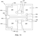
- FIGS. 11 and 12 illustrate further embodiments of routing (400, 500) on the interconnect layer 302.
- the at least one common source pad 280 is omitted for purposes of clarity in the figures.
- routing 400 includes two common source or Kelvin pads 470, and each common contact pad 470 is connected to two corresponding semiconductor devices 100 by trace connections 472.
- a gate bridge 490 includes a common gate pad 492 at least partially disposed in the overhang region 274 and gate contacts 496 connected by a trace connection 494 to each of the corresponding semiconductor devices 100.
- a routing 500 includes two common contact or Kelvin pads 570 at least partially disposed in the overhang region 274, and each common contact pad 570 is connected to two corresponding semiconductor devices 100 by the trace connections 572.
- the two common contact pads 570 are Kelvin contacts.
- a gate bridge 590 includes a common gate pad 592 at least partially disposed in the overhang region 274 and gate contacts 596 connected by a trace connection 594 to each of the corresponding semiconductor devices 100.
- the overhang region 274 and greater surface area of the POL-RDL package 250 facilitates using a wide range of common gate pads (292, 492, 592), common contact pads (370, 470, 570) and associated trace connections (294, 494, 594, 372, 472, 572). Placement of the common gate pads (292, 492, 592) and the at least one package contact pad 370 at least partially on the overhang region 274 also facilitates improved creepage control between components.
- the POL-RDL package 250 also enables an improved elastic (Young's) modulus of the first interconnect layer 260, which reduces bonding stress on the semiconductor devices 100.
- the first interconnect layer 260 of the POL-RDL package 250 may be polyimide, which has an elastic modulus of approximately 2.5 GPa, whereas the semiconductor devices 100, which may be SiO 2 , may have an elastic modulus of approximately 70 GPa.
- the lower elastic modulus is capable of absorbing bonding stress, thereby reducing bonding stress on the semiconductor devices 100.
- the POL-RDL package 250 can thus buffer the stresses during wire bonding to protect semiconductor devices 100.
- the trace connections (294, 494, 594, 372, 472, 572) may have varying resistivity values and various trace configuration structures. Using different types of trace configurations enables selectively tuning of the resistivity value between the common gate pad (292, 492, 592) and gate contacts (296, 496, 596).
- the common gate pads and common contact pads may be subsequently connected to package gate pads and package contact pads on additional interconnect layers. Notably, additional resistance reduces crosstalk, thus improving efficiency of the semiconductor devices 100.
- the resistance values can be selectively adjusted for specific applications without altering the semiconductor devices 100 during fabrication and assembly. This allows for simplified fabrication of the plurality of semiconductor devices 100 and binning during fabrication.
- the resistivity value of the trace connections (294, 494, 594, 372, 472, 572) can be altered by depositing the trace connection with material having different resistivities, by modifying a width of the trace connection, and/or by modifying a deposition thickness of the trace connection.
- An exemplary trace connection (294, 494, 594, 372, 472, 572) having a length of 2 mm, a width of 35 mm and a thickness of 10 mm has a resistance of approximately 0.1 ⁇ .
- the trace connection (294, 494, 594, 372, 472, 572) has a thickness in the range of 5-25 mm, and a trace width of approximately 25 mm.
- the trace connection (294, 494, 594, 372, 472, 572) deposition depth is in a range from 50 nanometers (nm) to 50 micrometers ( ⁇ m).
- the resistivity value of the trace connections (294, 494, 594, 372, 472, 572) is tuned or altered by changing the volume of the trace connection (294, 494, 594, 372, 472, 572), changing the cross-sectional area of the trace connection (294, 494, 594, 372, 472, 572), and/or changing the material of the trace connection (294, 494, 594, 372, 472, 572).
- the trace connection (294, 494, 594, 372, 472, 572) is made from a combination of a first material having a first resistivity value and a second material having a second resistivity value, and the second material is laminated or otherwise layered over the first material.
- the resistivity value of the trace connection (294, 494, 594, 372, 472, 572) may be selectively adjustable within a range of 10mQ (micro-ohms) to 100mS2.
- the trace connection (294, 494, 594, 372, 472, 572) is a resistor.
- the trace connection (294, 494, 594, 372, 472, 572) is a surface-mounted resistor.
- the resistor 176 can be connected post-fabrication, enabling resistance values to be changed to meet different application needs post-fabrication.
- the at least one common source pad 280 and the common gate pad 292 of the gate bridge 290 must have a sufficient surface area to make the electrical connection.
- the complexity and the surface area of the at least one common source pad 280 and the gate bridge 290 are ultimately limited by the overall surface area of the first interconnect layer 260.
- gate pads in a POL package may have a surface area of up to 0.6 square millimeters (mm 2 ) without the benefit of the overhang region 274.
- the common gate pad 292 of the gate bridge 290 has a surface area in the range of 0.5 mm 2 to 1.5 mm 2 while still maintaining the current rating of the multi-chip semiconductor package 200.
- the overhang region 274 of the POL-RDL package 250 allows for redistribution and more complex configurations of the common gate pad 292 of the gate bridge 290 while still maintaining the current rating of the semiconductor device 100 as shown in FIGS. 9-12 .
- the overhang region 274 of the POL-RDL package 250 allows for redistribution and more complex routing configurations of additional interconnect layers while still maintaining the current rating of the multi-chip semiconductor package 200 as shown in FIGS. 9-12 .
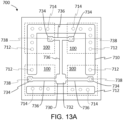
- FIG. 13A illustrates an alternative embodiment of routing 702 disposed on a first interconnect layer
- FIG. 13B illustrates associated routing 800 of a interconnect layer disposed over the first interconnect layer.
- the first and interconnect layers include components similar to the first interconnect layer 260 and the interconnect layer 302 previously described with reference to FIGS. 1-10B .
- the routing 700 of the first interconnect layer includes a first common source pad 710, a second common source pad 712 and a gate bridge 730.
- the common source pads (710, 712) are electrically connected to underlying semiconductor devices 100 by source via pathways 714 extending through the first interconnect layer.
- the gate bridge 730 includes a common gate pad 732 and gate contacts 734 connected by trace connections 736.
- the trace connections 736 are electrically connected to underlying semiconductor devices 100 by gate via pathways 738 extending through the first interconnect layer. As shown in FIG.
- the routing 800 of the interconnect layer includes a package contact pad 810 electrically connected to the first common source pad 710 and second common source pad 712, and a package gate pad 830 electrically connected to the common gate pad 732.
- the package contact pad 810 is electrically connected to the first common source pad 710 and second common source pad 712 by an intermediate metal interconnect layer 802.
- a gate attachment pad 832 is electrically connected to the common gate pad 732 (of FIG. 13A ), and the gate attachment pad 832 is connected to the package gate pad 830 by a trace connection 834.
- the trace connection 834 includes a surface-mounted resistor 836.
- the resistor 836 can be connected post-fabrication, enabling resistance values to be changed to meet different application needs post-fabrication.
- the trace connection 834 includes attachment pads for mounting the surface-mounted resistor 836 post-fabrication.
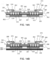
- FIGS. 14A-14B illustrate cross-sectional views of backside structures 900 connected to a bottom surface 111 of the semiconductor devices 100.
- the cross-sectional views are taken along line C-C' of FIG. 9B .
- the bottom surface 111 of the semiconductor devices 100 includes a drain pad and remains exposed.
- a sputter layer 902 is sputtered on the bottom surface 111 of the drain pad.
- the sputter layer 902 facilitates electrical and thermal contact to the backside using solder, sinter silver or conductive paste.
- the sputter layer 902 substantially covers the entire bottom surface 111 of the semiconductor devices 100, and in some embodiments, the sputter layer 902 substantially covers the molding.
- an electrically conductive plate 904 is then applied to the sputter layer 902.
- the electrically conductive plate 720 is a direct-bond copper DBC-type substrate.
- sputter layer 902 and the electrically conductive plate 904 are applied to the bottom surface 111 of the semiconductor devices 100 prior to applying the molding 102.
- the molding 102 extends below the bottom surface 111 of the semiconductor devices 100 and the bottom surface 111 of the semiconductor devices 100 remains partially exposed such that a partial encasement is formed.
- the sputter layer 902 is filled within gaps of the encasement such that the sputter layer 902 is co-planar with the molding 102.
- the electrically conductive plate 904 is then applied to the sputter layer 902.
- FIGS. 15A-15B illustrate one embodiment of a method 1000 of manufacturing a multi-chip semiconductor package, such as the previously described multi-chip semiconductor package 200.
- the method 1000 includes adhering 1002 an adhesive layer to a first interconnect layer of a POL-RDL package and forming 1004 at least one source via pathway and at least one gate via pathway through the first interconnect layer and the adhesive layer.
- the method 1000 further includes aligning 1006 at least one source pad and a gate pad of a plurality of semiconductor devices with the least one source via pathway and the at least one gate via pathway respectively, and adhering 1008 the plurality of semiconductor devices to the adhesive layer.
- the method further includes filling 1010 the least one source via pathway and the at least one gate via pathway respectively defined in the first interconnect layer with at least one metallization via.
- the method 1000 further includes depositing 1012 at least one common source pad and a gate bridge over the at least one gate via pathway respectively.
- the method 1000 further includes layering 1014 a interconnect layer over the first interconnect layer and forming 1016 least one source via pathway and at least one gate via pathway in the interconnect layer.
- the method 1000 further includes filling 1018 the least one source via pathway and the at least one gate via pathway respectively defined in the interconnect layer with at least one metallization via.
- the method 1000 further includes depositing 1020 a package contact pad and a package gate pad over the least one source via pathway and the at least one gate via pathway respectively defined in the interconnect layer.
- the method 1000 further includes depositing 1022 a sputter layer layered over a bottom surface of said plurality of semiconductor devices, said sputter layer electrically connected to drain connections of said at least one common source pad of said plurality of semiconductor devices. In some embodiments, the method 1000 further includes applying 1024 an electrically conductive plate over a bottom surface of said sputter layer.
- the metallization layers are formed through a combination of sputtering and electroplating applications, although it is recognized that other electroless methods of metal deposition could also be used.
- a titanium adhesion layer and a copper seed layer may first be applied via a sputtering process, followed by an electroplating process that increases a thickness of the copper to a desired level.
- the applied metal material is then subsequently patterned into metal interconnects having a desired shape and that function as vertical feed-throughs formed through the interconnect layer and the adhesive layer.
- the embodiments overcome at least some disadvantages of semiconductor devices. Specifically, the embodiments improve surface bonding onto contact pads of a POL structure.
- the overhang region of the POL structure reduces bonding stresses on the semiconductor devices.
- the overhang region of the POL structure allows for redistribution of the components of the POL-RDL package and the second laminated interconnect layers and allows for contact pads having a greater surface areas.
- the overhang region also allows for a wider range of utilization of trace connections with varying resistivity.
- the POL-RDL package also allows for multiple semiconductor devices to operate as a single device having a common gate pad and a common source pad.
- the individual semiconductor devices can be binned and grouped into devices having similar characteristics, thereby eliminating devices that have wafer defects. This permits the formation of multi-chip semiconductor packages that go beyond practical yield limits as opposed to fabricating a single large and complex semiconductor package.
- the multi-chip semiconductor device allows for 5mOHM device when tiled together. By way of example, but not limitation, binning four 20mOHM semiconductor devices into the multi-chip semiconductor package and connecting the semiconductor devices in parallel with the common gate pad and the common source pad results in a 5mOHM device.
- combining together multiple semiconductor devices into a multi-chip semiconductor package requires matching semiconductor devices having similar characteristics due to semiconductor manufacturing and fabrication processes inherently having yield variance of the individual semiconductor devices.
- density limitations of multi-chip semiconductor package manufacturing and assembly increases complexity of multi-chip semiconductor package designs. Such factors may alter the characteristics of the semiconductor device.
- the POL-RDL package and the described systems and methods facilitate tiling semiconductor devices together.
- Each semiconductor device may be individually binned for improved packaging without having to overcome variances in defect densities of larger semiconductor devices.
Landscapes
- Internal Circuitry In Semiconductor Integrated Circuit Devices (AREA)
- Physics & Mathematics (AREA)
- Geometry (AREA)
Abstract
Description
- The present disclosure relates generally to semiconductor packages, and more particularly to a multi-chip semiconductor package having an interconnecting power overlay structure.
- Power semiconductor devices, such as switches and rectifiers, are key components of power electronic circuits (e.g., switched mode power supplies, inverters, rectifiers, and the like). High power applications typically require multi-chip assemblies comprising multiple power semiconductor devices connected together to carry large amounts of current and to support high voltages. When connecting individual devices into multi-chip assemblies, it is important to maintain layout symmetry and low inductance interconnect in order to ensure good load sharing, minimize voltage and current overshoots, and reduce switching losses. A top surface of each power semiconductor device, such as metal oxide semiconductor field effect transistor (MOSFET), includes a gate pad and at least one source pad which are electrically connected to gate and source pads of other devices in the multi-chip assembly. The electrical connections of multiple gate pads and source pads are typically formed using wire bonds and complex routing configurations to a common gate pad and at least one common source pad. The common gate pad and at least one common source pad of the multi-chip semiconductor assembly may be connected to an external power electronic circuit such that the multi-chip semiconductor assembly operates as a singular power processing unit.
- An alternative to the wire bonding of gate pads and source pads may be the use of one or more planar interconnect layers separated by interconnect layers disposed over the top surfaces of the semiconductor devices. The interconnect layers may include metallization vias which extend through the interconnect layer to electrically couple the source pads and gate pads to the common gate pad and the common source pad disposed on upper interconnect layers of the multi-chip semiconductor assembly to deliver power to the semiconductor devices through the metallization vias.
- To establish a proper electrical connection to external power electronic circuitry, the common gate pad and the common source pad on an uppermost interconnect layer require sufficient surface area to solder, sinter, copper-bond, copper-clip, or otherwise connect the common gate pad and the source pad of the multi-chip assembly with the external power electronic circuitry. However, the available surface area of the common gate pad and the common source pad are generally limited by the overall surface area of the multi-chip semiconductor assembly. Further, direct soldering, sintering, copper-bonding, and copper-clipping onto smaller common gate pads and common source pads introduce bonding stresses onto the multi-chip semiconductor assembly and form less reliable interconnections.
- Additionally, connecting together multiple gate pads into the common gate pad and multiple source pads into the common source pad of a multi-chip semiconductor assembly requires good layout symmetry resulting in matched inductances of individual connections to ensure good load sharing among individual devices. Realizing high current power modules requires paralleling multiple semiconductor devices. For example, building a 480A power module will require paralleling of eight devices, each rated for approximately 60A. Paralleling eight devices is challenging from the aspect of ensuring all eight devices share current equally, due to their varying individual characteristics and the challenge to connect each device to the external power electronic circuitry such that each switch receives the signal to turn on or off at the same time. This is driven by gate-source parasitic impedance, which is driven by the geometry of traces connections between devices. The more devices in parallel, the more complicated it is to balance the impedance to ensure each device switches at the same time and shares current. One solution is to parallel two larger semiconductor devices, each rated at approximately 240A. A device rated at 240A is significantly larger than a device rated for 60A. This will make the packaging and interconnection easier, however, the device yield will be significantly lower.
- Finally, semiconductor fabrication processes inherently result in varying characteristics of individual semiconductor devices within wafer and wafer-to-wafer. Therefore, building multi-chip semiconductor assemblies from individual devices with similar characteristics will further maintain full performance of individual devices within a multi-chip assembly.
- In one aspect, a multi-chip semiconductor package is disclosed. The package includes an interconnect layer having an upper surface and a bottom surface, wherein the interconnect layer includes a dielectric material, at least one common source pad disposed on the upper surface of the interconnect layer, at least one common gate pad disposed on the upper surface of the interconnect layer, and a plurality of semiconductor devices each including a gate pad and at least one source pad adhered onto the interconnect layer, wherein the source pads of the plurality of semiconductor devices are electrically connected to the at least one common source pad, and wherein the source pads of the plurality of semiconductor devices are electrically connected in parallel with one another, and wherein the gate pads of the plurality of semiconductor devices are electrically connected to the common gate pad, and wherein the gate pads of the plurality of semiconductor devices are electrically connected in parallel with one another.
- In another aspect, a method of manufacturing a multi-chip semiconductor package is disclosed. The method includes forming at least one source via pathway and at least one gate via pathway through an interconnect layer, aligning at least one source pad and a gate pad of a plurality of semiconductor devices with the least one source via pathway and the at least one gate via pathway, respectively, and adhering the plurality of semiconductor devices to the interconnect layer, wherein a surface area of the interconnect layer is substantially equal to a surface area of a footprint defined by the plurality of semiconductor devices
- The subject-matter of the disclosure will be explained in more detail in the following text with reference to exemplary embodiments which are illustrated in the attached drawings.
-
FIG. 1 is a perspective view of one embodiment of a semiconductor device; -
FIG. 2 is perspective view of a one embodiment of a molding of a multi-chip semiconductor package; -
FIG. 3 is a perspective view of one embodiment of a multi-chip semiconductor package; -
FIG. 4 is a plan view of the multi-chip semiconductor package ofFIG. 3 ; -
FIG. 5 is an exploded view of the multi-chip semiconductor package ofFIG. 3 ; -
FIG. 6 is an exploded view of the multi-chip semiconductor package ofFIG. 3 ; -
FIG. 7 is a cross-sectional view of the multi-chip semiconductor package ofFIG. 3 taken along line A-A'; -
FIG. 8 is a cross-sectional view of the multi-chip semiconductor package ofFIG. 3 taken along line B-B'; -
FIG. 9A is a plan view of an example interconnect layer and associated routing in accordance with one or more embodiments of the present disclosure; -
FIG. 9B is a translucent plan view of an example interconnect layer and associated routing in accordance with one or more embodiments of the present disclosure; -
FIG. 9C is a cross-sectional view of the interconnect layer and associated routing ofFIG. 9B taken along line C-C'; -
FIG. 9D is a cross-sectional view of the interconnect layer and associated routing ofFIG. 9B taken along line D-D'; -
FIG. 10A is a plan view of an example interconnect layer and associated routing in accordance with one or more embodiments of the present disclosure; -
FIG. 10B is a plan view of an example interconnect layer and associated routing in accordance with one or more embodiments of the present disclosure; -
FIGS. 11 and12 are plan views of an example interconnect layer and associated routing in accordance with one or more embodiments of the present disclosure; -
FIG. 13A is a plan view of an example first interconnect layer and associated routing in accordance with one or more embodiments of the present disclosure; -
FIG. 13B is a plan view of an example interconnect layer and associated routing in accordance with one or more embodiments of the present disclosure; -
FIG. 13C is a plan view of an example interconnect layer and associated routing in accordance with one or more embodiments of the present disclosure; -
FIGS. 14A-14B are cross-sectional views of example backside structures; and, -
FIG. 15A-15B illustrate one embodiment of a method of manufacturing a multi-chip semiconductor package. - The reference symbols used in the drawings, and their meanings, are listed in summary form in the list of reference symbols. In principle, identical parts are provided with the same reference symbols in the figures.
- In the following specification and the claims, reference will be made to a number of terms, which shall be defined to have the following meanings.
- As used herein, the singular forms "a," "an," and "the" include plural references unless the context clearly dictates otherwise. The terms "comprising," "including," and "having" are intended to be inclusive and mean that there may be additional elements other than the listed elements. The terms "optional" or "optionally" means that the subsequently described event or circumstance may or may not occur, and that the description includes instances where the event occurs and instances where it does not.
- Unless otherwise indicated, approximating language, such as "generally," "substantially," and "about," as used herein indicates that the term so modified may apply to only an approximate degree, as would be recognized by one of ordinary skill in the art, rather than to an absolute or perfect degree. Accordingly, a value modified by a term or terms, such as "about," "approximately," and "substantially," is not to be limited to the precise value specified. In at least some instances, the approximating language may correspond to the precision of an instrument for measuring the value. Here and throughout the specification and claims, range limitations may be identified. Such ranges may be combined and/or interchanged, and include all the sub-ranges contained therein unless context or language indicates otherwise.
- Additionally, unless otherwise indicated, the terms "first," "second," etc. are used herein merely as labels, and are not intended to impose ordinal, positional, or hierarchical requirements on the items to which these terms refer. Moreover, reference to, for example, a "second" item does not require or preclude the existence of, for example, a "first" or lower-numbered item or a "third" or higher-numbered item.
- Embodiments of the disclosure relate generally to structures and methods for packaging multiple semiconductor devices and, more particularly to multi-chip semiconductor package having an interconnecting power overlay (POL) structure. The methods, systems, and apparatus described herein overcome at least some disadvantages of at least some known multi-chip semiconductor packages. More specifically, the systems and apparatus described herein provide a POL package configured as a redistribution layer (RDL) positioned directly over multiple semiconductor devices. Accordingly, the POL package is also referred to herein as a POL-RDL package. The POL-RDL package includes an oversized surface area relative to a footprint of the molding defined by the semiconductor devices (or more generally to a footprint of the semiconductor devices), which improves available surface area for placement of common gate pads, common source pads and overlayed contact pads. The oversized surface area also allows for placement of more complex configurations of common source pads, common gate pads and gate bridges, and additional interconnect layers and interconnect layers.
- A multi-chip semiconductor package is disclosed. The multi-chip semiconductor package includes least one interconnect layer having an upper surface and a bottom surface, at least one common source pad disposed on the upper surface of the at least one interconnect layer, at least one common gate pad disposed on the upper surface of the at least one interconnect layer and, a plurality of semiconductor devices. Each of the semiconductor devices have a gate pad and at least one source pad adhered onto a bottom surface of a first interconnect layer of the at least one interconnect layer. The bottom surface of the first interconnect layer has an adhesive layer. The source pads of the plurality of semiconductor devices are electrically connected to the at least one common source pad, and the source pads of the plurality of semiconductor devices are electrically connected in parallel with one another. The gate pads of the plurality of semiconductor devices are electrically connected to the at least one common gate pad, and the gate pads of the plurality of semiconductor devices are electrically connected in parallel with one another.
- As used herein, the term "routing" refers to metallization vias disposed within via pathways of a interconnect layer and to trace connections, pads, contacts and contact pads disposed on the interconnect layer. The routing may also include surface-mount resistors, thin film resistors and associated pads for placement of surface-mount resistors post-fabrication.
- Additional interconnect layers and routing may be laminated or otherwise fabricated over a first interconnect layer to facilitate additional routing configurations. As used herein, the terms "package gate pad" and "package source pad" refer to common gate pads and common source pads on an uppermost interconnect layer which are electrically connected to external power electronic circuitry. Any of the first interconnect layer and additional interconnect layers disclosed herein may be directly connected to external power electronic circuitry or may have additional interconnect layers and routing. Therefore, the terms "package gate pad," "package source pad," "common gate pads," and "common source pads" are used interchangeably.
-
FIG. 1 illustrates a perspective view of one embodiment of asemiconductor device 100.FIG. 2 illustrates a perspective view of amolding 102 including at least two semiconductor devices 100 (also referred to as a plurality of semiconductor devices 100). As shown inFIGS. 1 and 2 , thesemiconductor device 100 includes adielectric material 106 that defines anupper surface 101. Thesemiconductor device 100 further includes at least onesource pad 110 and agate pad 120 disposed on theupper surface 101 of thesemiconductor device 100. The at least onesource pad 110 includes atop contact surface 112. Likewise, thegate pad 120 includes atop contact surface 122. - The
top contact surfaces gate pad 120 and each of the at least onesource pad 110 are electrically isolated from each other by thedielectric material 106. In some embodiments, at least a portion of thegate pad 120 and the at least onesource pad 110 at least partially extend below theupper surface 101. In some embodiments, thetop contact surface 112 of the at least onesource pad 110 and thetop contact surface 122 of thegate pad 120 are flush with the surface of thedielectric material 106. In some embodiments, thetop contact surface 112 of the at least onesource pad 110 and thetop contact surface 122 of thegate pad 120 are below the surface of thedielectric material 106. In some embodiments, thetop contact surface 112 of the at least onesource pad 110 and thetop contact surface 122 of thegate pad 120 are above the surface of thedielectric material 106. - As shown in
FIG. 2 , themolding 102 includes aunderfill material 103 that defines anupper surface 104, and a plurality ofsemiconductor devices 100 at least partially disposed in themolding 102 and surrounded by theunderfill material 103. The plurality ofsemiconductor devices 100 embedded in themolding 102 define a footprint 105 (as best shown inFIG. 4 ).FIGS. 3-8 illustrate one or more embodiments of amulti-chip semiconductor package 200.FIG. 3 illustrates a perspective view of themulti-chip semiconductor package 200,FIG. 4 illustrates a plan, partially transparent view of thesemiconductor package 200 andFIGS. 5 and6 illustrate exploded views of thesemiconductor package 200.FIGS. 7 and 8 illustrate cross-sectional views of thesemiconductor package 200 taken along lines A-A' and B-B' ofFIG. 4 , respectively. - The
multi-chip semiconductor package 200 operates as a metal-oxide-semiconductor field-effect transistor (MOSFET) having two ormore semiconductor devices 100. Themulti-chip semiconductor package 200 includes a POL-RDL package 250 having at least onecommon source pad 280 and agate bridge 290. The POL-RDL package 250 includes afirst interconnect layer 260 and anadhesive layer 262 disposed over the molding 102 (as best shown inFIG. 5 ). In some embodiments, thefirst interconnect layer 260 is in the form of a lamination or a film, and may be formed of one a plurality of dielectric materials, such as Kapton® polyimide, Ultem® polyetherimide, polytetrafluoroethylene (PTFE), Upilex®, polysulfone materials (e.g., Udel® polysulphone, Radel® polyphenolsulphone), or another polymer film, such as a liquid crystal polymer (LCP), Bismaleimide-Triazine resin, Ajinomoto Build-up Film® ABF or a polyimide material. In one embodiment, the POL-RDL package 250 has a total thickness in the range of 25 microns to 300 microns. - In some embodiments, the POL-RDL package 250 (which may include any number of
interconnect layers 260, trace connections, source and gate pads) is fully fabricated and positioned over the molding 102 (together with the plurality ofsemiconductor devices 100 embedded in the molding 102), and thefirst interconnect layer 260 is adhered to thesource pads 110 and thegate pads 120 by theadhesive layer 262. That is, theadhesive layer 262 is positioned between thefirst interconnect layer 260 and themolding 102. In some embodiments, thesemiconductor devices 100 may be adhered directly onto theadhesive layer 262 without a molding. A molding or an underfill material may be deposited between thesemiconductor devices 100 at a later stage. - In operation, metallization vias are formed in source via
pathways 264 and gate viapathways 266 extending through the first interconnect layer 260 (and in any number of additional interconnect layers as explained in further detail below with reference toFIGS. 9A - 14B ), associated metal interconnect structures and routing are built over the first interconnect layer 260 (and in any number of additional interconnect layers), and theadhesive layer 262 is applied to a bottom surface of thefirst interconnect layer 260. The semiconductor devices 100 (either as part of themolding 102 or individually) are aligned with the source viapathways 264 and gate viapathways 266 extending through the first interconnect layer 160 in accordance with one or more configurations, and themolding 102 is cured to form themulti-chip semiconductor package 200. It is understood that any of the steps in fabrication may be performed in a different sequence. By way of example, the source viapathways 264 and gate viapathways 266 may be filled prior to aligning and adhering the semiconductor devices 100 (either as part of themolding 102 or individually). - The at least one
common source pad 280 and thegate bridge 290 are formed on anupper surface 261 of thefirst interconnect layer 260. Source viapathways 264 and gate viapathways 266 extend through thefirst interconnect layer 260 and theadhesive layer 262. As best shown inFIGS. 7 and 8 , the POL-RDL package 250 of themulti-chip semiconductor package 200 also includes ametal interconnect structure 267 that extends through the source viapathways 264 and the gate viapathways 266. Themetal interconnect structure 267 electrically couples thetop contact surface 112 of each of thesource pads 110 to the at least onecommon source pad 280 of the POL-RDL package 250, and likewise themetal interconnect structure 267 electrically couples thetop contact surface 122 of thegate pad 120 to thegate bridge 290 of the POL-RDL package 250. - In some embodiments, the
metal interconnect structure 267 is formed by filling the source viapathways 264 and the gate viapathways 266 with a conductive material (i.e., conductive epoxy, paste, or solder and the like). In some embodiments, the vias have plated copper and a sputtered adhesion layer such as titanium or Ti-tungsten. In some embodiments, themetal interconnect structure 267 is formed during deposition of the at least onecommon source pad 280 and thegate bridge 290. By way of example, as the at least onecommon source pad 280 and thegate bridge 290 are deposited, the source viapathways 264 and the gate viapathways 266 are also filled. Subsequently, the at least onecommon source pad 280 and thegate bridge 290 are electroplated or otherwise plated or fabricated to a desired thickness. - In some embodiments, the
gate bridge 290 includes acommon gate pad 292 andgate contacts 296 connected bytrace connections 294. As best shown inFIG. 6 , each of thegate contacts 296 of thegate bridge 290 are aligned with thegate pads 120 of the plurality ofsemiconductor devices 100. As shown inFIGS. 7 and 8 , thecommon gate pad 292, thetrace connection 294, and thegate contacts 296 are disposed on thefirst interconnect layer 260 of the POL-RDL package 250, and thegate contacts 296 are electrically connected to thegate pads 120 by themetal interconnect structure 267. Thetrace connection 294 extends from thecommon gate pad 292 to thegate contacts 296, and may have any number of branches and bends to establish the electrical connection between thecommon gate pad 292 and thegate contacts 296. In the illustrated embodiments, thegate bridge 290 has an I-shape with each end being a pair ofgate contacts 296 that align withgate pads 120 of the plurality ofsemiconductor devices 100, however as shown inFIGS. 11 through 13A , thegate bridge 290 can have other shapes and configurations but maintain equal path lengths, as explained in further detail below. - As shown in
FIG. 4 , thetrace connections 294 of thegate bridge 290 have the same length between thecommon gate pad 292 andgate contacts 296 such that there are equal resistivity values between thecommon gate pad 292 andgate contacts 296. The length of thetrace connections 294 impacts inductance. To alternatively achieve substantially equal resistivities, thecommon gate pad 292 and the length of thetrace connections 294 can be made similar to all thegate pads 120 of thesemiconductor devices 100. However, depending on how the source is connected, it may create asymmetry in the gate source loop inductance which is a key parameter. The POL-RDL package 250 provides for flexibility in optimizing the gate-source loop inductance depending on how it is oriented and connected to the next level circuit. For example, the resistivity and trance length of two of thesemiconductor devices 100 to be different than the other twosemiconductor devices 100 so that the eventual gate source loops to each device is similar/equal. - To achieve
trace connections 294 having equal length and equal resistivity values, thesemiconductor devices 100 can be oriented or positioned on theadhesive layer 262 and thefirst interconnect layer 260 such that thegate pad 120 of each of the semiconductor devices are an equal length from thecommon gate pad 292 of thegate bridge 290. In some embodiments, any one of thetrace connections 294 may include a surface-mount resistor or a thin-film resistor to balance resistivity values. - As shown in
FIGS. 2 ,4 , and7 , an outerperipheral edge 108 of theunderfill material 103 defines a surface area of themolding 102. Each of the plurality of thesemiconductor devices 100 are spaced from the outerperipheral edge 108 of themolding 102, and the placement of the plurality of thesemiconductor devices 100 in themolding 102 defines afootprint 105 of the molding 102 (please note thefootprint 105, as defined herein, generally has a smaller surface than themolding 102 itself). It is understood that in some embodiments, the plurality of thesemiconductor devices 100 are directly adhered to the first interconnect layer 260 (and adhesive layer 262) without the use of themolding 102, and in such embodiments, thefootprint 105 is defined as the placement of the plurality ofsemiconductor devices 100 on the bottom surface of thefirst interconnect layer 260. Thefootprint 105 is therefore defined as the outermost peripheral edges of the plurality of thesemiconductor devices 100. - The
first interconnect layer 260 of the POL-RDL package 250 is generally placed over theentire molding 102 and has a surface area greater than thefootprint 105 of themolding 102 such that an outerperipheral edge 268 of thefirst interconnect layer 260 extends beyond thefootprint 105 of themolding 102 and the outermost peripheral edges of the plurality of semiconductor devices 100 (please note that the outerperipheral edge 268 does not extend beyond a perimeter of the molding itself 102). In some embodiments, theadhesive layer 262 extends to the outerperipheral edge 268 of thefirst interconnect layer 260. - In some embodiments, the
overhang region 274 of the POL-RDL package 250 increases available surface area of thefirst interconnect layer 260 for placement of a largercommon source pad 280 and a larger common gate pad 292.Theoverhang region 274 also allows for placement of more complex configurations ofcommon source pads 280, gate bridges 290,common gate pads 292 and trace connections for thecommon source pads 280 andcommon gate pads 292 as explained in further detail below. The POL-RDL package 250 thus facilitates improved routing and more robust connections of the at least onecommon source pad 280 and thecommon gate pad 292 to external power electronic circuitry or to additional interconnect layers disposed over the first interconnect layer 260 (as explained in further detail below). Connection of external power electronic circuitry - either directly onto the at least onecommon source pad 280 and thecommon gate pad 292 or by the additional interconnect layers - enables thesource pads 110 of the plurality ofsemiconductor devices 100 to be used for electricity control and conversion. By way of example, thesource pads 110 of the plurality ofsemiconductor devices 100 may be configured to turn power received fromrespective gate pads 120 on and off thousands of times per second. The at least onecommon source pad 280 and thecommon gate pad 292 establish an input-output (I/O) connection for thesource pads 110 andrespective gate pads 120 by way of themetal interconnect structure 267. The input-output (I/O) connection enables connection of themulti-chip semiconductor package 200 to an external power electronic circuit, such as a printed circuit board (PCB). - In at least some embodiments, a surface area of the POL-RDL package 250 (e.g., a surface area of the first interconnect layer 260) is substantially equal to a surface area of the
footprint 105 defined by the plurality ofsemiconductor devices 100. For example, the surface area of the POL-RDL package 250 may be between 10% larger than the surface area of thefootprint footprint 105 and 5% smaller than the surface area of the footprint, and even more particularly may be between 2% larger than the surface area of thefootprint 105 and 5% smaller than the surface area of the footprint. -
FIGS. 9A though 9D illustrate embodiments of routing 300 of ainterconnect layer 302 positioned over thefirst interconnect layer 260.FIG. 9A illustrates a top view of theinterconnect layer 302 and associatedrouting 300.FIG. 9B illustrates a top translucent view of theinterconnect layer 302 and associatedrouting 300.FIG. 9C illustrates a cross-sectional view of theinterconnect layer 302 and associated routing 300 taken along line C-C', andFIG. 9D illustrates a cross-sectional view of the of theinterconnect layer 302 and associatedrouting 300. Theinterconnect layer 302 is layered on the POL-RDL package 250 (and thefirst interconnect layer 260 specifically), and includes pads and trace connections similar to components shown in themulti-chip semiconductor package 200 ofFIGS. 1-8 . - The
interconnect layer 302 is applied over thefirst interconnect layer 260 of the POL-RDL package 250. Theinterconnect layer 302 includes at least onepackage contact pad 370 and apackage gate pad 390 which facilitate connection of themulti-chip semiconductor package 200 to external power electronic circuitry. The electrical connections include one or more of soldering, sintering, copper-bonding, copper-clipping and the like. In some embodiments, additional interconnect layers may be laminated over theinterconnect layer 302 to facilitate more complex routing from the at least onepackage contact pad 370 and thepackage gate pad 390. In some embodiments, the at least onepackage contact pad 370 is a Kelvin contact. -
Trace connections 372 extend from the at least onepackage contact pad 370 toattachment pads 374, and may have any number of branches and bends to establish an electrical connection to underlying structures such as thecommon source pad 280 of thefirst interconnect layer 260. Thecommon source pad 280 of thefirst interconnect layer 260 is electrically connected to theattachment pads 374 by metal interconnect viapathways 362 extending through theinterconnect layer 302. The interconnect viapathways 362 are aligned with the at least onecommon source pad 280 for deposition of a metal interconnect structure that extends through the interconnect viapathways 362. - The
interconnect layer 302 includes gate viapathways 392 for connecting thecommon gate pad 292 to thepackage gate pad 390 on theinterconnect layer 302. In some embodiments, the metal interconnect structure is formed by filling the interconnect viapathways 362 and the gate viapathways 392 with a conductive material (i.e., conductive epoxy, paste, or solder and the like). In some embodiments, the metal interconnect structure is formed during deposition of the at least onepackage contact pad 370,trace connections 372,attachment pads 374 and thepackage gate pad 390. - The
overhang region 274 and greater surface area of the POL-RDL package 250 facilitate complex routing. As shown inFig. 9B , thetrace connections 372 extend into the overhang region, however it is understood that thetrace connections 372 may extend across the at least onecommon source pad 280 of thefirst interconnect layer 260. By way of example, but not limitation,FIG. 10A illustrates an embodiment where thetrace connections 372 extend across the at least onecommon source pad 280 of thefirst interconnect layer 260. - Referring back to
FIGS. 9A and9B , thetrace connections 372 at least partially extend into theoverhang region 274, and thegate bridge 290 has an I-shape. Each of thegate contacts 296 and thetrace connections 294 of thegate bridge 290 are equidistant from thecommon gate pad 292 such that thegate contacts 296 have the same resistivity. In the illustrated embodiment, theinterconnect layer 302 includes twocommon contact pads 370, and eachcommon contact pad 370 is connected to twocorresponding semiconductor devices 100 by theattachment pads 374 and thetrace connections 372. In some embodiments, there is at least oneattachment pad 374 for eachsemiconductor device 100. The twocommon contact pads 370 and thecommon gate pad 292 are configured as an input-output (I/O) connection for themulti-chip semiconductor package 200 to external power electronic circuitry. - As shown in
FIG. 10B , in some embodiments, agate attachment pad 394 is electrically connected to thecommon gate pad 292 of the gate bridge 290 (as shown inFIG. 9B ) by the gate viapathways 392. Thepackage gate pad 390 is electrically connected to thegate attachment pad 394 by atrace connection 396. In some embodiments, thetrace connection 396 includes a surface-mountedresistor 398. In some embodiments, theresistor 398 can be connected post-fabrication, enabling resistance values to be changed to meet different application needs post-fabrication. In some embodiments, thetrace connection 396 includes attachment pads for mounting the surface-mountedresistor 398 post-fabrication. -
FIGS. 11 and12 illustrate further embodiments of routing (400, 500) on theinterconnect layer 302. InFIGS. 11 and12 , the at least onecommon source pad 280 is omitted for purposes of clarity in the figures. - As shown in
FIG. 11 , one embodiment ofrouting 400 includes two common source orKelvin pads 470, and eachcommon contact pad 470 is connected to twocorresponding semiconductor devices 100 bytrace connections 472. Agate bridge 490 includes acommon gate pad 492 at least partially disposed in theoverhang region 274 andgate contacts 496 connected by atrace connection 494 to each of thecorresponding semiconductor devices 100. - As shown in
FIG. 12 , another embodiment of arouting 500 includes two common contact orKelvin pads 570 at least partially disposed in theoverhang region 274, and eachcommon contact pad 570 is connected to twocorresponding semiconductor devices 100 by the trace connections 572. In some embodiments, the twocommon contact pads 570 are Kelvin contacts. Agate bridge 590 includes acommon gate pad 592 at least partially disposed in theoverhang region 274 andgate contacts 596 connected by atrace connection 594 to each of thecorresponding semiconductor devices 100. - The
overhang region 274 and greater surface area of the POL-RDL package 250 facilitates using a wide range of common gate pads (292, 492, 592), common contact pads (370, 470, 570) and associated trace connections (294, 494, 594, 372, 472, 572). Placement of the common gate pads (292, 492, 592) and the at least onepackage contact pad 370 at least partially on theoverhang region 274 also facilitates improved creepage control between components. The POL-RDL package 250 also enables an improved elastic (Young's) modulus of thefirst interconnect layer 260, which reduces bonding stress on thesemiconductor devices 100. Thefirst interconnect layer 260 of the POL-RDL package 250 may be polyimide, which has an elastic modulus of approximately 2.5 GPa, whereas thesemiconductor devices 100, which may be SiO2, may have an elastic modulus of approximately 70 GPa. The lower elastic modulus is capable of absorbing bonding stress, thereby reducing bonding stress on the semiconductor devices 100.The POL-RDL package 250 can thus buffer the stresses during wire bonding to protectsemiconductor devices 100. - The trace connections (294, 494, 594, 372, 472, 572) may have varying resistivity values and various trace configuration structures. Using different types of trace configurations enables selectively tuning of the resistivity value between the common gate pad (292, 492, 592) and gate contacts (296, 496, 596). The common gate pads and common contact pads may be subsequently connected to package gate pads and package contact pads on additional interconnect layers. Notably, additional resistance reduces crosstalk, thus improving efficiency of the
semiconductor devices 100. In accordance with the embodiments described herein, the resistance values can be selectively adjusted for specific applications without altering thesemiconductor devices 100 during fabrication and assembly. This allows for simplified fabrication of the plurality ofsemiconductor devices 100 and binning during fabrication. - For example, the resistivity value of the trace connections (294, 494, 594, 372, 472, 572) can be altered by depositing the trace connection with material having different resistivities, by modifying a width of the trace connection, and/or by modifying a deposition thickness of the trace connection. An exemplary trace connection (294, 494, 594, 372, 472, 572) having a length of 2 mm, a width of 35 mm and a thickness of 10 mm has a resistance of approximately 0.1 Ω. In some embodiments, the trace connection (294, 494, 594, 372, 472, 572) has a thickness in the range of 5-25 mm, and a trace width of approximately 25 mm. In some embodiments, the trace connection (294, 494, 594, 372, 472, 572) deposition depth is in a range from 50 nanometers (nm) to 50 micrometers (µm). In some embodiments, the resistivity value of the trace connections (294, 494, 594, 372, 472, 572) is tuned or altered by changing the volume of the trace connection (294, 494, 594, 372, 472, 572), changing the cross-sectional area of the trace connection (294, 494, 594, 372, 472, 572), and/or changing the material of the trace connection (294, 494, 594, 372, 472, 572). In some embodiments, the trace connection (294, 494, 594, 372, 472, 572) is made from a combination of a first material having a first resistivity value and a second material having a second resistivity value, and the second material is laminated or otherwise layered over the first material. The resistivity value of the trace connection (294, 494, 594, 372, 472, 572) may be selectively adjustable within a range of 10mQ (micro-ohms) to 100mS2. In some embodiments, the trace connection (294, 494, 594, 372, 472, 572) is a resistor. Further, in some embodiments, the trace connection (294, 494, 594, 372, 472, 572) is a surface-mounted resistor. In some embodiments, the resistor 176 can be connected post-fabrication, enabling resistance values to be changed to meet different application needs post-fabrication.
- To establish a proper connection to external power electronic circuitry, the at least one
common source pad 280 and thecommon gate pad 292 of thegate bridge 290 must have a sufficient surface area to make the electrical connection. However, the complexity and the surface area of the at least onecommon source pad 280 and thegate bridge 290 are ultimately limited by the overall surface area of thefirst interconnect layer 260. By way of example, in at least some known semiconductor assemblies, gate pads in a POL package may have a surface area of up to 0.6 square millimeters (mm2) without the benefit of theoverhang region 274. Without the benefit of the additional surface area provided by theoverhang region 274, a larger gate pad would necessarily reduce the available area for placement of a source pad, resulting in a lower current rating of each of themulti-chip semiconductor package 200. In contrast, in at least some of the embodiments described herein, thecommon gate pad 292 of thegate bridge 290, given the benefit of theoverhang region 274, has a surface area in the range of 0.5 mm2 to 1.5 mm2 while still maintaining the current rating of themulti-chip semiconductor package 200. Theoverhang region 274 of the POL-RDL package 250 allows for redistribution and more complex configurations of thecommon gate pad 292 of thegate bridge 290 while still maintaining the current rating of thesemiconductor device 100 as shown inFIGS. 9-12 . Similar to thegate bridge 290, theoverhang region 274 of the POL-RDL package 250 allows for redistribution and more complex routing configurations of additional interconnect layers while still maintaining the current rating of themulti-chip semiconductor package 200 as shown inFIGS. 9-12 . -
FIG. 13A illustrates an alternative embodiment of routing 702 disposed on a first interconnect layer, andFIG. 13B illustrates associated routing 800 of a interconnect layer disposed over the first interconnect layer. The first and interconnect layers include components similar to thefirst interconnect layer 260 and theinterconnect layer 302 previously described with reference toFIGS. 1-10B . - As shown in
FIG. 13A , therouting 700 of the first interconnect layer includes a firstcommon source pad 710, a secondcommon source pad 712 and agate bridge 730. The common source pads (710, 712) are electrically connected tounderlying semiconductor devices 100 by source viapathways 714 extending through the first interconnect layer. Thegate bridge 730 includes acommon gate pad 732 andgate contacts 734 connected bytrace connections 736. Thetrace connections 736 are electrically connected tounderlying semiconductor devices 100 by gate viapathways 738 extending through the first interconnect layer. As shown inFIG. 13B , therouting 800 of the interconnect layer includes apackage contact pad 810 electrically connected to the firstcommon source pad 710 and secondcommon source pad 712, and apackage gate pad 830 electrically connected to thecommon gate pad 732. Thepackage contact pad 810 is electrically connected to the firstcommon source pad 710 and secondcommon source pad 712 by an intermediatemetal interconnect layer 802. - As shown in
FIG. 13C , in some embodiments agate attachment pad 832 is electrically connected to the common gate pad 732 (ofFIG. 13A ), and thegate attachment pad 832 is connected to thepackage gate pad 830 by atrace connection 834. In some embodiments, thetrace connection 834 includes a surface-mountedresistor 836. In some embodiments, theresistor 836 can be connected post-fabrication, enabling resistance values to be changed to meet different application needs post-fabrication. In some embodiments, thetrace connection 834 includes attachment pads for mounting the surface-mountedresistor 836 post-fabrication. -
FIGS. 14A-14B illustrate cross-sectional views of backside structures 900 connected to abottom surface 111 of thesemiconductor devices 100. The cross-sectional views are taken along line C-C' ofFIG. 9B . - As shown in
FIG. 14A , thebottom surface 111 of thesemiconductor devices 100 includes a drain pad and remains exposed. Asputter layer 902 is sputtered on thebottom surface 111 of the drain pad. Thesputter layer 902 facilitates electrical and thermal contact to the backside using solder, sinter silver or conductive paste. Thesputter layer 902 substantially covers the entirebottom surface 111 of thesemiconductor devices 100, and in some embodiments, thesputter layer 902 substantially covers the molding. As shown inFIG. 14B , an electricallyconductive plate 904 is then applied to thesputter layer 902. In some embodiments, the electrically conductive plate 720 is a direct-bond copper DBC-type substrate. - As shown in
FIG. 14A ,sputter layer 902 and the electricallyconductive plate 904 are applied to thebottom surface 111 of thesemiconductor devices 100 prior to applying the molding 102.As shown inFIG. 14B , themolding 102 extends below thebottom surface 111 of thesemiconductor devices 100 and thebottom surface 111 of thesemiconductor devices 100 remains partially exposed such that a partial encasement is formed. Thesputter layer 902 is filled within gaps of the encasement such that thesputter layer 902 is co-planar with themolding 102. The electricallyconductive plate 904 is then applied to thesputter layer 902. -
FIGS. 15A-15B illustrate one embodiment of amethod 1000 of manufacturing a multi-chip semiconductor package, such as the previously describedmulti-chip semiconductor package 200. Themethod 1000 includes adhering 1002 an adhesive layer to a first interconnect layer of a POL-RDL package and forming 1004 at least one source via pathway and at least one gate via pathway through the first interconnect layer and the adhesive layer. - The
method 1000 further includes aligning 1006 at least one source pad and a gate pad of a plurality of semiconductor devices with the least one source via pathway and the at least one gate via pathway respectively, and adhering 1008 the plurality of semiconductor devices to the adhesive layer. The method further includes filling 1010 the least one source via pathway and the at least one gate via pathway respectively defined in the first interconnect layer with at least one metallization via. Themethod 1000 further includes depositing 1012 at least one common source pad and a gate bridge over the at least one gate via pathway respectively. - In some embodiments, the
method 1000 further includes layering 1014 a interconnect layer over the first interconnect layer and forming 1016 least one source via pathway and at least one gate via pathway in the interconnect layer. Themethod 1000 further includes filling 1018 the least one source via pathway and the at least one gate via pathway respectively defined in the interconnect layer with at least one metallization via. Themethod 1000 further includes depositing 1020 a package contact pad and a package gate pad over the least one source via pathway and the at least one gate via pathway respectively defined in the interconnect layer. - In some embodiments, the
method 1000 further includes depositing 1022 a sputter layer layered over a bottom surface of said plurality of semiconductor devices, said sputter layer electrically connected to drain connections of said at least one common source pad of said plurality of semiconductor devices. In some embodiments, themethod 1000 further includes applying 1024 an electrically conductive plate over a bottom surface of said sputter layer. - In some embodiments, the metallization layers are formed through a combination of sputtering and electroplating applications, although it is recognized that other electroless methods of metal deposition could also be used. For example, a titanium adhesion layer and a copper seed layer may first be applied via a sputtering process, followed by an electroplating process that increases a thickness of the copper to a desired level. The applied metal material is then subsequently patterned into metal interconnects having a desired shape and that function as vertical feed-throughs formed through the interconnect layer and the adhesive layer.
- The above-described embodiments overcome at least some disadvantages of semiconductor devices. Specifically, the embodiments improve surface bonding onto contact pads of a POL structure. In particular, the overhang region of the POL structure reduces bonding stresses on the semiconductor devices. The overhang region of the POL structure allows for redistribution of the components of the POL-RDL package and the second laminated interconnect layers and allows for contact pads having a greater surface areas. The overhang region also allows for a wider range of utilization of trace connections with varying resistivity.
- The POL-RDL package also allows for multiple semiconductor devices to operate as a single device having a common gate pad and a common source pad. The individual semiconductor devices can be binned and grouped into devices having similar characteristics, thereby eliminating devices that have wafer defects. This permits the formation of multi-chip semiconductor packages that go beyond practical yield limits as opposed to fabricating a single large and complex semiconductor package. Furthermore, the multi-chip semiconductor device allows for 5mOHM device when tiled together. By way of example, but not limitation, binning four 20mOHM semiconductor devices into the multi-chip semiconductor package and connecting the semiconductor devices in parallel with the common gate pad and the common source pad results in a 5mOHM device.
- As previously set forth. combining together multiple semiconductor devices into a multi-chip semiconductor package requires matching semiconductor devices having similar characteristics due to semiconductor manufacturing and fabrication processes inherently having yield variance of the individual semiconductor devices. In addition density limitations of multi-chip semiconductor package manufacturing and assembly increases complexity of multi-chip semiconductor package designs. Such factors may alter the characteristics of the semiconductor device. The POL-RDL package and the described systems and methods facilitate tiling semiconductor devices together. Each semiconductor device may be individually binned for improved packaging without having to overcome variances in defect densities of larger semiconductor devices.
- The methods, systems, and compositions disclosed herein are not limited to the specific embodiments described herein, but rather, steps of the methods, elements of the systems, and/or elements of the compositions may be utilized independently and separately from other steps and/or elements described herein.
- Although specific features of various embodiments may be shown in some drawings and not in others, this is for convenience only. Moreover, references to "one embodiment" in the above description are not intended to be interpreted as excluding the existence of additional embodiments that also incorporate the recited features. In accordance with the principles of the disclosure, any feature of a drawing may be referenced and/or claimed in combination with any feature of any other drawing.
- This written description uses examples, including the best mode, to enable any person skilled in the art to practice the disclosure, including making and using any devices or systems and performing any incorporated methods. The patentable scope of the disclosure is defined by the claims, and may include other examples that occur to those skilled in the art. Such other examples are intended to be within the scope of the claims if they have structural elements that do not differ from the literal language of the claims, or if they include equivalent structural elements with insubstantial differences from the literal languages of the claims.
- Further aspects of the disclosure are provided by the subject matter of the following clauses.
- 1. A multi-chip semiconductor package comprising:
- an interconnect layer having an upper surface and a bottom surface, wherein said interconnect layer comprises a dielectric material,
- at least one common source pad disposed on said upper surface of said interconnect layer;
- at least one common gate pad disposed on said upper surface of said interconnect layer; and
- a plurality of semiconductor devices each comprising a gate pad and at least one source pad adhered onto said interconnect layer;
- wherein said source pads of said plurality of semiconductor devices are electrically connected to said at least one common source pad, and wherein said source pads of said plurality of semiconductor devices are electrically connected in parallel with one another; and
- wherein said gate pads of said plurality of semiconductor devices are electrically connected to said common gate pad, and wherein said gate pads of said plurality of semiconductor devices are electrically connected in parallel with one another.
- 2. The multi-chip semiconductor package of any preceding clause, further comprising an adhesive layer disposed on said bottom surface of said interconnect layer.
- 3. The multi-chip semiconductor package of any preceding clause, further comprising a plurality of gate contacts disposed on said interconnect layer and electrically connected to said common gate pad by trace connections, wherein each gate pad of each of said plurality of semiconductor devices is connected to an associated gate contact of said plurality of gate contacts.
- 4. The multi-chip semiconductor package of any preceding clause, wherein said plurality of gate contacts are equidistant from said common gate pad.
- 5. The multi-chip semiconductor package of any preceding clause, wherein said gate trace connections have an equal resistivity value.
- 6. The multi-chip semiconductor package of any preceding clause, wherein at least one trace connection of said trace connections comprises one of a surface-mount resistor and a thin-film resistor.
- 7. The multi-chip semiconductor package of any preceding clause, wherein said common gate pad and said at least one common source pad are configured to be electrically connected to external power electronic circuitry such that said POL-RDL package operates as a singular processing unit.
- 8. The multi-chip semiconductor package of any preceding clause, further comprising a Kelvin contact electrically connected to said at least one common source pad to facilitate connecting said at least one common source pad to the external power electronic circuitry.
- 9. The multi-chip semiconductor package of any preceding clause, further comprising:
- an additional interconnect layer disposed over said interconnect layer;
- a package gate pad disposed on said additional interconnect layer and electrically connected to said common gate pad of said interconnect layer; and
- at least one package source pad disposed on said additional interconnect layer and electrically connected to said at least one common source pad of said interconnect layer.
- 10. The multi-chip semiconductor package of any preceding clause, wherein said package gate pad is electrically connected to a gate attachment pad by a trace connection, said gate attachment pad connected to said common gate pad of said interconnect layer.
- 11. The multi-chip semiconductor package of any preceding clause, wherein said trace connection electrically connected to said package gate pad comprises one of a surface-mount resistor and a thin-film resistor.
- 12. The multi-chip semiconductor package of any preceding clause, wherein said package gate pad and said at least one package source pad are configured to be electrically connected to external power electronic circuitry such that said POL-RDL package operates as a singular power switching unit.
- 13. The multi-chip semiconductor package of any preceding clause, wherein a surface area of said interconnect layer is substantially equal to a surface area of a footprint defined by the plurality of semiconductor devices.
- 14. The multi-chip semiconductor package of any preceding clause, wherein a backside of the semiconductor devices are electrically connected together by an electrically conductive plate such that a common drain connection is formed.
- 15. The multi-chip semiconductor package of any preceding clause, further comprising a molding disposed between said interconnect layer and said electrically conductive plate.
- 16. A method of manufacturing a multi-chip semiconductor package, the method comprising:
- forming at least one source via pathway and at least one gate via pathway through an interconnect layer, the interconnect layer including a dielectric material;
- aligning at least one source pad and a gate pad of a plurality of semiconductor devices with the least one source via pathway and the at least one gate via pathway, respectively; and
- adhering the plurality of semiconductor devices to the interconnect layer, wherein a surface area of the interconnect layer is substantially equal to a surface area of a footprint defined by the plurality of semiconductor devices.
- 17. The method of any preceding clause, further comprising:
- filling the least one source via pathway and the at least one gate via pathway with at least one metallization via; and
- depositing at least one common source pad and a gate bridge over the at least one gate via pathway.
- 18. The method of any preceding clause, further comprising:
- layering an additional interconnect layer over the first interconnect layer;
- forming least one source via pathway and at least one gate via pathway in the additional interconnect layer; and,
- filling the least one source via pathway and the at least one gate via pathway respectively defined in the additional interconnect layer with at least one second metallization via.
- 19. The method of any preceding clause, further comprising depositing a package contact pad and a package gate pad over the least one source via pathway and the at least one gate via pathway respectively defined in the additional interconnect layer.
- 20. The method of any preceding clause, further comprising:
- depositing a sputter layer layered over a bottom surface of the plurality of semiconductor devices to form a common drain connection; and
- applying an electrically conductive plate over a bottom surface of the sputter layer.
Claims (15)
- A multi-chip semiconductor package (200) comprising:an interconnect layer (260) having an upper surface (261) and a bottom surface, wherein said interconnect layer comprises a dielectric material,at least one common source pad (280) disposed on said upper surface of said interconnect layer;at least one common gate pad (292) disposed on said upper surface of said interconnect layer; anda plurality of semiconductor devices (100) each comprising a gate pad (120) and at least one source pad (110) adhered onto said interconnect layer;wherein said source pads of said plurality of semiconductor devices are electrically connected to said at least one common source pad, and wherein said source pads of said plurality of semiconductor devices are electrically connected in parallel with one another; andwherein said gate pads of said plurality of semiconductor devices are electrically connected to said common gate pad, and wherein said gate pads of said plurality of semiconductor devices are electrically connected in parallel with one another.
- The multi-chip semiconductor package (200) of claim 1 further comprising an adhesive layer (262) disposed on said bottom surface of said interconnect layer (260).
- The multi-chip semiconductor package (200) of any preceding claim, further comprising a plurality of gate contacts (296) disposed on said interconnect layer (260) and electrically connected to said common gate pad (292) by trace connections (294), wherein each gate pad (120) of each of said plurality of semiconductor devices (100) is connected to an associated gate contact of said plurality of gate contacts.
- The multi-chip semiconductor package (200) of claim 3, wherein said plurality of gate contacts (296) are equidistant from said common gate pad (292).
- The multi-chip semiconductor package (200) of any preceding claim, wherein said gate trace connections (294) have an equal resistivity value.
- The multi-chip semiconductor package (200) of claim 5, wherein at least one trace connection (294) of said trace connections comprises one of a surface-mount resistor and a thin-film resistor.
- The multi-chip semiconductor package (200) of claim 3, wherein said common gate pad (292) and said at least one common source pad (280) are configured to be electrically connected to external power electronic circuitry such that said POL-RDL package (250) operates as a singular processing unit.
- The multi-chip semiconductor package (200) of claim 7 further comprising a Kelvin contact (470) electrically connected to said at least one common source pad (280) to facilitate connecting said at least one common source pad to the external power electronic circuitry.
- The multi-chip semiconductor (200) package of claim 1, further comprising:an additional interconnect layer (302) disposed over said interconnect layer (260);a package gate pad (390) disposed on said additional interconnect layer and electrically connected to said common gate pad (292) of said interconnect layer; andat least one package source pad (280) disposed on said additional interconnect layer and electrically connected to said at least one common source pad of said interconnect layer.
- The multi-chip semiconductor package (200) of claim 9, wherein said package gate pad (390) is electrically connected to a gate attachment pad (394) by a trace connection (396), said gate attachment pad connected to said common gate pad of said interconnect layer (260).
- The multi-chip semiconductor package (200) of claim 10, wherein said trace connection (396) electrically connected to said package gate pad (390) comprises one of a surface-mount resistor and a thin-film resistor.
- The multi-chip semiconductor package (200) of any one of claims 9-11, wherein said package gate pad (390) and said at least one package source pad are configured to be electrically connected to external power electronic circuitry such that said POL-RDL package (250) operates as a singular power switching unit.
- The multi-chip semiconductor package (200) of any preceding claim, wherein a surface area of said interconnect layer (260) is substantially equal to a surface area of a footprint defined by the plurality of semiconductor devices (100).
- The multi-chip semiconductor package (200) of any preceding claim, wherein a backside of the semiconductor devices (100) are electrically connected together by an electrically conductive plate (720) such that a common drain connection is formed.
- The multi-chip semiconductor package (200) of claim 14 further comprising a molding (102) disposed between said interconnect layer (260) and said electrically conductive plate (720).
Applications Claiming Priority (1)
| Application Number | Priority Date | Filing Date | Title |
|---|---|---|---|
| US18/234,603 US20250062280A1 (en) | 2023-08-16 | 2023-08-16 | Power overlay structure for a multi-chip semiconductor package |
Publications (1)
| Publication Number | Publication Date |
|---|---|
| EP4510185A1 true EP4510185A1 (en) | 2025-02-19 |
Family
ID=92264099
Family Applications (1)
| Application Number | Title | Priority Date | Filing Date |
|---|---|---|---|
| EP24193418.1A Pending EP4510185A1 (en) | 2023-08-16 | 2024-08-07 | Power overlay structure for a multi-chip semiconductor package |
Country Status (5)
| Country | Link |
|---|---|
| US (1) | US20250062280A1 (en) |
| EP (1) | EP4510185A1 (en) |
| JP (1) | JP7786790B2 (en) |
| KR (1) | KR102930577B1 (en) |
| CN (1) | CN119495676A (en) |
Citations (4)
| Publication number | Priority date | Publication date | Assignee | Title |
|---|---|---|---|---|
| US20100109052A1 (en) * | 2008-11-05 | 2010-05-06 | Renesas Technology Corp. | Semiconductor device and manufacturing method thereof |
| US20160126212A1 (en) * | 2014-10-31 | 2016-05-05 | Infineon Technologies Ag | Chip assemblage, press pack cell and method for operating a press pack cell |
| US11177188B1 (en) * | 2020-07-23 | 2021-11-16 | Actron Technology Corporation | Heat dissipation substrate for multi-chip package |
| US20220115298A1 (en) * | 2020-10-12 | 2022-04-14 | Nxp Usa, Inc. | Power amplifier modules with flip-chip and non-flip-chip power transistor dies |
Family Cites Families (14)
| Publication number | Priority date | Publication date | Assignee | Title |
|---|---|---|---|---|
| JP3712111B2 (en) * | 2001-03-30 | 2005-11-02 | ユーディナデバイス株式会社 | Power amplification semiconductor device |
| US8629453B2 (en) * | 2008-04-28 | 2014-01-14 | International Rectifier Corporation | Externally configurable integrated circuits |
| JP2012104513A (en) * | 2010-11-05 | 2012-05-31 | Toshiba Corp | Semiconductor device, semiconductor assembly member, and manufacturing method of the semiconductor device |
| JP2013149805A (en) * | 2012-01-19 | 2013-08-01 | Fuji Electric Co Ltd | Semiconductor device and method of manufacturing semiconductor device |
| US10312167B2 (en) * | 2017-02-15 | 2019-06-04 | Infineon Technologies Ag | Semiconductor package, assembly and module arrangements for measuring gate-to-emitter/source voltage |
| EP3376539A1 (en) * | 2017-03-14 | 2018-09-19 | HS Elektronik Systeme GmbH | Stackable power module |
| CN111033735B (en) * | 2017-09-04 | 2023-05-23 | 三菱电机株式会社 | Semiconductor module and power conversion device |
| US10354871B2 (en) * | 2017-09-11 | 2019-07-16 | General Electric Company | Sputtering system and method for forming a metal layer on a semiconductor device |
| JP7367506B2 (en) * | 2019-12-12 | 2023-10-24 | 株式会社プロテリアル | semiconductor module |
| JP7494613B2 (en) * | 2020-07-17 | 2024-06-04 | 富士電機株式会社 | Semiconductor Device |
| JP7407675B2 (en) * | 2020-08-18 | 2024-01-04 | 株式会社 日立パワーデバイス | Power semiconductor modules and power conversion devices |
| US11515235B2 (en) * | 2020-10-30 | 2022-11-29 | Gan Systems Inc. | Device topology for lateral power transistors with low common source inductance |
| JP7856283B2 (en) * | 2021-11-26 | 2026-05-11 | 国立大学法人東北大学 | Power semiconductor elements and power semiconductor modules |
| WO2025211720A1 (en) * | 2024-04-01 | 2025-10-09 | 주식회사 엘엑스세미콘 | Power semiconductor module and power conversion apparatus |
-
2023
- 2023-08-16 US US18/234,603 patent/US20250062280A1/en active Pending
-
2024
- 2024-08-07 EP EP24193418.1A patent/EP4510185A1/en active Pending
- 2024-08-14 KR KR1020240108975A patent/KR102930577B1/en active Active
- 2024-08-14 CN CN202411112699.0A patent/CN119495676A/en active Pending
- 2024-08-16 JP JP2024136985A patent/JP7786790B2/en active Active
Patent Citations (4)
| Publication number | Priority date | Publication date | Assignee | Title |
|---|---|---|---|---|
| US20100109052A1 (en) * | 2008-11-05 | 2010-05-06 | Renesas Technology Corp. | Semiconductor device and manufacturing method thereof |
| US20160126212A1 (en) * | 2014-10-31 | 2016-05-05 | Infineon Technologies Ag | Chip assemblage, press pack cell and method for operating a press pack cell |
| US11177188B1 (en) * | 2020-07-23 | 2021-11-16 | Actron Technology Corporation | Heat dissipation substrate for multi-chip package |
| US20220115298A1 (en) * | 2020-10-12 | 2022-04-14 | Nxp Usa, Inc. | Power amplifier modules with flip-chip and non-flip-chip power transistor dies |
Also Published As
| Publication number | Publication date |
|---|---|
| KR102930577B1 (en) | 2026-02-25 |
| US20250062280A1 (en) | 2025-02-20 |
| JP2025028043A (en) | 2025-02-28 |
| KR20250027490A (en) | 2025-02-26 |
| JP7786790B2 (en) | 2025-12-16 |
| CN119495676A (en) | 2025-02-21 |
Similar Documents
| Publication | Publication Date | Title |
|---|---|---|
| US10497648B2 (en) | Embedded electronics package with multi-thickness interconnect structure and method of making same | |
| US7977763B2 (en) | Chip package with die and substrate | |
| KR102392414B1 (en) | Electrical interconnect structure for an embedded semiconductor device package and method of manufacturing thereof | |
| US9589920B2 (en) | Chip package | |
| US10504826B1 (en) | Device almost last embedded device structure and method of manufacturing thereof | |
| US8653670B2 (en) | Electrical interconnect for an integrated circuit package and method of making same | |
| CN110970387B (en) | Semiconductor device and method of forming semiconductor device | |
| US20190043802A1 (en) | Method of manufacturing an electronics package using device-last or device-almost last placement | |
| US9570376B2 (en) | Electrical interconnect for an integrated circuit package and method of making same | |
| US20130333924A1 (en) | Multilayer electronic support structure with integral metal core | |
| US10692737B2 (en) | Multilayer interconnect structure with buried conductive via connections and method of manufacturing thereof | |
| US20250062280A1 (en) | Power overlay structure for a multi-chip semiconductor package | |
| US11869844B2 (en) | Semiconductor device | |
| US20230145182A1 (en) | Semiconductor device | |
| US12635544B2 (en) | Power overlay package for a semiconductor device coupled to a POL-RDL package | |
| EP4560703A2 (en) | Power overlay package for a semiconductor device | |
| JP2023071300A (en) | Semiconductor device | |
| JP2023071585A (en) | Semiconductor device |
Legal Events
| Date | Code | Title | Description |
|---|---|---|---|
| PUAI | Public reference made under article 153(3) epc to a published international application that has entered the european phase |
Free format text: ORIGINAL CODE: 0009012 |
|
| STAA | Information on the status of an ep patent application or granted ep patent |
Free format text: STATUS: THE APPLICATION HAS BEEN PUBLISHED |
|
| AK | Designated contracting states |
Kind code of ref document: A1 Designated state(s): AL AT BE BG CH CY CZ DE DK EE ES FI FR GB GR HR HU IE IS IT LI LT LU LV MC ME MK MT NL NO PL PT RO RS SE SI SK SM TR |
|
| STAA | Information on the status of an ep patent application or granted ep patent |
Free format text: STATUS: REQUEST FOR EXAMINATION WAS MADE |
|
| 17P | Request for examination filed |
Effective date: 20250811 |
|
| REG | Reference to a national code |
Ref country code: DE Ref legal event code: R079 Free format text: PREVIOUS MAIN CLASS: H01L0023640000 Ipc: H01L0023000000 |
|
| GRAP | Despatch of communication of intention to grant a patent |
Free format text: ORIGINAL CODE: EPIDOSNIGR1 |
|
| STAA | Information on the status of an ep patent application or granted ep patent |
Free format text: STATUS: GRANT OF PATENT IS INTENDED |
|
| RIC1 | Information provided on ipc code assigned before grant |
Ipc: H01L 23/00 20060101AFI20251112BHEP Ipc: H01L 25/07 20060101ALI20251112BHEP |
|
| INTG | Intention to grant announced |
Effective date: 20251205 |
|
| GRAJ | Information related to disapproval of communication of intention to grant by the applicant or resumption of examination proceedings by the epo deleted |
Free format text: ORIGINAL CODE: EPIDOSDIGR1 |
|
| STAA | Information on the status of an ep patent application or granted ep patent |
Free format text: STATUS: REQUEST FOR EXAMINATION WAS MADE |
|
| REG | Reference to a national code |
Ref country code: DE Ref legal event code: R079 Free format text: PREVIOUS MAIN CLASS: H01L0023000000 Ipc: H10W0070600000 |
|
| GRAP | Despatch of communication of intention to grant a patent |
Free format text: ORIGINAL CODE: EPIDOSNIGR1 |
|
| STAA | Information on the status of an ep patent application or granted ep patent |
Free format text: STATUS: GRANT OF PATENT IS INTENDED |
|
| INTC | Intention to grant announced (deleted) | ||
| RIC1 | Information provided on ipc code assigned before grant |
Ipc: H10W 70/60 20260101AFI20260323BHEP Ipc: H10W 90/00 20260101ALI20260323BHEP |
|
| INTG | Intention to grant announced |
Effective date: 20260402 |