EP4510170A1 - Josephson junction element, quantum device, and production method for josephson junction element - Google Patents
Josephson junction element, quantum device, and production method for josephson junction element Download PDFInfo
- Publication number
- EP4510170A1 EP4510170A1 EP22937398.0A EP22937398A EP4510170A1 EP 4510170 A1 EP4510170 A1 EP 4510170A1 EP 22937398 A EP22937398 A EP 22937398A EP 4510170 A1 EP4510170 A1 EP 4510170A1
- Authority
- EP
- European Patent Office
- Prior art keywords
- insulating film
- film
- superconducting
- region
- superconducting film
- Prior art date
- Legal status (The legal status is an assumption and is not a legal conclusion. Google has not performed a legal analysis and makes no representation as to the accuracy of the status listed.)
- Pending
Links
Images








Classifications
-
- H—ELECTRICITY
- H10—SEMICONDUCTOR DEVICES; ELECTRIC SOLID-STATE DEVICES NOT OTHERWISE PROVIDED FOR
- H10N—ELECTRIC SOLID-STATE DEVICES NOT OTHERWISE PROVIDED FOR
- H10N60/00—Superconducting devices
- H10N60/10—Junction-based devices
- H10N60/12—Josephson-effect devices
-
- H—ELECTRICITY
- H10—SEMICONDUCTOR DEVICES; ELECTRIC SOLID-STATE DEVICES NOT OTHERWISE PROVIDED FOR
- H10N—ELECTRIC SOLID-STATE DEVICES NOT OTHERWISE PROVIDED FOR
- H10N60/00—Superconducting devices
- H10N60/01—Manufacture or treatment
- H10N60/0912—Manufacture or treatment of Josephson-effect devices
Definitions
- the present disclosure relates to a Josephson junction device, a quantum device, and a method for manufacturing the Josephson junction device.
- the Josephson junction device includes two superconducting films and an insulating film between the two superconducting films.
- one superconducting film included in a Josephson junction device is processed by reactive ion etching after film formation, and damage inevitably occurs in the vicinity of a side surface of the superconducting film remaining after the processing.
- damage occurs in the superconducting film
- properties of the Josephson junction between a region where this damage has occurred and the other superconducting film can vary.
- damage inevitably occurs also in the insulating film.
- the Josephson junction includes a region of the insulating film where damage has occurred, the properties of the Josephson junction can vary.
- An object of the present disclosure is to provide a Josephson junction device, a quantum device, and a method for manufacturing the Josephson junction device capable of obtaining stable properties.
- a Josephson junction device including: a first superconducting film; a first insulating film provided over the first superconducting film; and a second superconducting film provided over the first insulating film, in which a surface layer portion of the first insulating film includes a first region and a second region around the first region, electrical insulation properties of the first region are higher than the electrical insulation properties of the second region, and the second superconducting film is located at an inner side of a boundary between the first region and the second region in plan view.
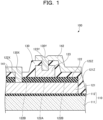
- FIG. 1 is a cross-sectional view illustrating a Josephson junction device according to the first embodiment.
- FIG. 2 is a plan view illustrating the Josephson junction device according to the first embodiment.
- FIG. 1 corresponds to a cross-sectional view taken along line I-I in FIG. 2 .
- a wire line 141, a wire line 142, and an insulating film 130 are omitted.
- a Josephson junction device 100 mainly includes a substrate 110, a superconducting film 121, an insulating film 122, a superconducting film 123, the insulating film 130, the wire line 141, and the wire line 142.
- the substrate 110 includes, for example, a silicon (Si) substrate 111 and an insulating film 112.
- the insulating film 112 is formed over the silicon substrate 111.
- the insulating film 112 is, for example, a silicon oxide film.
- the substrate 110 is a so-called oxide film-attached substrate.
- the superconducting film 121 is provided over the insulating film 112.
- the superconducting film 121 is, for example, a niobium (Nb) film having a thickness of about 200 nm.
- the insulating film 122 is provided over the superconducting film 121.
- the insulating film 122 is, for example, an aluminum oxide (Al) film having a thickness of about 20 nm.
- the superconducting film 123 is provided over the insulating film 122.
- the superconducting film 123 is, for example, a niobium film having a thickness of about 200 nm.
- the superconducting film 121 is an example of a first superconducting film
- the insulating film 122 is an example of a first insulating film
- the superconducting film 123 is an example of a second superconducting film.
- a surface layer portion of the insulating film 122 includes a first region 122A and a second region 122B around the first region 122A. Greater damage has occurred in the second region 122B than the first region 122A, and the electrical insulation properties of the second region 122B are lower than the electrical insulation properties of the first region 122A. That is, the electrical insulation properties of the first region 122A are higher than the electrical insulation properties of the second region 122B.
- the superconducting film 123 is provided over the first region 122A. In plan view, the superconducting film 123 is located at an inner side of a boundary between first region 122A and second region 122B.
- the magnitude of damage in the first region 122A and the second region 122B can be specified using, for example, a transmission electron microscope (TEM).
- TEM transmission electron microscope
- a groove 121Z is formed in the superconducting film 121, and a groove 122Z is formed in the insulating film 122.
- the groove 122Z communicates with the groove 121Z, and the insulating film 112 is exposed through the grooves 121Z and 122Z.
- the grooves 121Z and 122Z are, for example, grooves for device separation.
- the insulating film 130 covers the substrate 110, the superconducting film 121, the insulating film 122, and the superconducting film 123.
- the insulating film 130 is, for example, a silicon oxide film.
- a contact hole 122X is formed in the insulating film 122, and a contact hole 130X is formed in the insulating film 130.
- the contact hole 130X communicates with the contact hole 122X, and the superconducting film 121 is exposed through the contact holes 122X and 130X.
- the contact hole 122X passes through the second region 122B, for example.
- the wire line 141 is provided over the insulating film 130 and also is in contact with the superconducting film 121 through the contact holes 122X and 130X.
- the wire line 141 is, for example, a niobium film.
- a contact hole 130Y is formed in the insulating film 130.
- the superconducting film 123 is exposed through the contact hole 130Y.
- a recess 123Y communicating with the contact hole 130Y may be formed on a surface of the superconducting film 123.
- the wire line 142 is provided over the insulating film 130 and also is in contact with the superconducting film 123 through the contact hole 130Y.
- the wire line 142 is, for example, a niobium film.
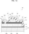
- FIGs. 3 to 12 are cross-sectional views illustrating a method for manufacturing the Josephson junction device according to the first embodiment.
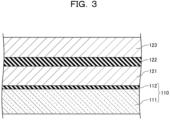
- the substrate 110 including the silicon substrate 111 and the insulating film 112 is prepared, and the superconducting film 121, the insulating film 122, and the superconducting film 123 are formed over the insulating film 112.
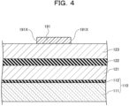
- a resist pattern 191 is formed over the superconducting film 123.
- the resist pattern 191 includes an opening 191X.
- the opening 191X approximately overlaps a region where the second region 122B of the insulating film 122 is to be formed.
- the superconducting film 123 is etched with the resist pattern 191 as a mask.
- This etching is, for example, reactive ion etching (RIE) using a reactive gas 150 containing sulfur hexafluoride (SF 6 ) as a main component.
- RIE reactive ion etching
- SF 6 sulfur hexafluoride
- This etching is performed until the insulating film 122 is exposed.
- a portion of the superconducting film 123 covered with the resist pattern 191 remains.
- a vicinity of a side surface of the remaining superconducting film 123 is damaged by etching, and a damaged region 123B is formed in the vicinity of the side surface of the superconducting film 123.
- the superconducting film 123 has an internal region 123A not damaged by etching on an inner side of the damaged region 123B.
- a vicinity of an upper surface of the insulating film 122 is also damaged by etching, and the first region 122A and the second region 122B around the first region 122A are formed in a surface layer portion of the insulating film 122.
- etching damage greater than the etching damage in the first region 122A has occurred, and the electrical insulation properties of the second region 122B becomes lower than the electrical insulation properties of the first region 122A.
- the first region 122A is formed at an inner side of an outer edge of the resist pattern 191 in plan view.
- the resist pattern 191 is removed.
- the damaged region 123B is removed by etching the superconducting film 123.
- This etching is, for example, isotropic etching such as wet etching.
- the superconducting film 123 is etched by about 20 nm in a direction parallel to a surface of the substrate 110. That is, the superconducting film 123 is reduced in plan view by isotropic etching.
- the superconducting film 123 is positioned over the first region 122A and is positioned at an inner side of the boundary between the first region 122A and the second region 122B in plan view.
- the etchant for example, a hydrogen fluoride (HF) solution, a mixed solution of HF and H 2 O 2 , a mixed solution of HF, H 2 SO 4 , and HNO 3 , or a mixed solution of HF and HNO 3 can be used.
- a hydrogen fluoride (HF) solution for example, a hydrogen fluoride (HF) solution, a mixed solution of HF and H 2 O 2 , a mixed solution of HF, H 2 SO 4 , and HNO 3 , or a mixed solution of HF and HNO 3
- a diluted hydrochloric acid (HCl) solution or a diluted H 2 SO 4 solution can be used as the etchant.
- a resist pattern 192 is formed over the insulating film 122 and the superconducting film 123.
- the resist pattern 192 includes an opening 192Z. In plan view, the opening 192Z overlaps a region where the grooves 121Z and 122Z are to be formed.
- the insulating film 122 is milled with the resist pattern 192 as a mask.
- the groove 122Z is formed in the insulating film 122.
- the superconducting film 123 is etched with the resist pattern 192 as a mask. This etching is, for example, RIE using a reactive gas containing sulfur hexafluoride as a main component.
- the groove 121Z is formed in the superconducting film 121.
- the resist pattern 192 is removed. Thereafter, the insulating film 130 covering the substrate 110, the superconducting film 121, the insulating film 122, and the superconducting film 123 is formed.
- the insulating film 130 is formed by, for example, a chemical vapor deposition (CVD) method.
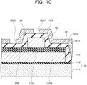
- a resist pattern 193 is formed over the insulating film 130.
- the resist pattern 193 includes openings 193X and 193Y.
- the opening 193X overlaps a region where the contact holes 122X and 130X are to be formed
- the opening 193Y overlaps a region where the contact hole 130Y is to be formed.
- the insulating film 130 is etched with the resist pattern 193 as a mask.
- This etching is, for example, RIE using a reactive gas containing fluorocarbon (CF 4 ) as a main component.
- CF 4 reactive gas containing fluorocarbon
- the contact holes 130X and 130Y are formed in the insulating film 130.
- the insulating film 122 is milled with the resist pattern 193 as a mask.
- the contact hole 130X is formed in the insulating film 122.
- the recess 123Y may be formed in a portion of the superconducting film 123 exposed from the contact hole 130Y.
- the wire line 141 in contact with the superconducting film 121 through the contact holes 122X and 130X and the wire line 142 in contact with the superconducting film 123 through the contact hole 130Y are formed over the insulating film 130.
- the Josephson junction device 100 can be manufactured. Since the miniaturization of the Josephson junction device increases the proportion of a region of the superconducting film where damage has occurred, a change in properties is likely to become significant. Therefore, the present invention is particularly effective in such a case.
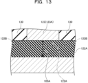
- FIG. 13 is an enlarged cross-sectional view illustrating a part of FIG. 1 .
- FIG. 14 is a cross-sectional view illustrating a portion corresponding to the Josephson junction device in FIG. 13 according to the reference example.
- the first region 122A and the second region 122B have been produced in the surface layer portion of the insulating film 122, and damage due to the RIE (see FIG. 5 ) has occurred in the second region 122B, whereas damage due to the RIE has not occurred in the first region 122A. That is, in the second region 122B, greater damage than damage in the first region 122A has occurred.
- the superconducting film 123 is located at an inner side of the boundary between the first region 122A and the second region 122B in plan view. Therefore, a Josephson junction 100A between the superconducting film 121 and the superconducting film 123 is spaced from the second region 122B. Consequently, according to the first embodiment, stable properties may be obtained.
- the superconducting film 123 includes the damaged region 123B, and the superconducting film 123 straddles the boundary between the first region 122A and the second region 122B and includes a portion outside this boundary in plan view.
- the superconducting film 121 and the superconducting film 123 there are not only the Josephson junction 100A spaced from the second region 122B, but also a Josephson junction 100B including the second region 122B.
- the Josephson junction 100B sometimes includes a Josephson junction between the superconducting film 121 and the damaged region 123B. Accordingly, in the reference example, the properties are easy to vary.
- FIG. 15 is a cross-sectional view illustrating a Josephson junction device according to the second embodiment.
- FIG. 16 is a plan view illustrating the Josephson junction device according to the second embodiment.
- FIG. 15 corresponds to a cross-sectional view taken along line XV-XV in FIG. 16 .
- a wire line 141, a wire line 142, and an insulating film 130 are omitted.
- a Josephson junction device 200 mainly includes a substrate 110, a superconducting film 121, an insulating film 122, a superconducting film 123, an insulating film 224, the insulating film 130, the wire line 141, and the wire line 142.
- the insulating film 224 is provided over the superconducting film 123.
- the insulating film 224 is, for example, an aluminum oxide film having a thickness of about 20 nm. That is, the material of the insulating film 224 is of the same type as the type of the material of the insulating film 122, and a thickness of the insulating film 224 is equal to a thickness of the insulating film 122.
- the insulating film 224 is an example of a second insulating film.
- the insulating film 130 covers the substrate 110, the superconducting film 121, the insulating film 122, the superconducting film 123, and the insulating film 224.
- the insulating film 130 is an example of a third insulating film.
- a contact hole 122X is formed in the insulating film 122, and a contact hole 130X is formed in the insulating film 130.
- the contact hole 130X communicates with the contact hole 122X, and the superconducting film 121 is exposed through the contact holes 122X and 130X.
- the contact hole 122X passes through a second region 122B, for example.
- the wire line 141 is provided over the insulating film 130 and also is in contact with the superconducting film 121 through the contact holes 122X and 130X.
- the wire line 141 is an example of a first wire line.
- the contact holes 122X and 130X are examples of a first opening.
- a contact hole 224Y is formed in the insulating film 224.
- a contact hole 130Y communicates with the contact hole 224Y, and the superconducting film 123 is exposed through the contact holes 224Y and 130Y.
- the recess 123Y is not formed on a surface of the superconducting film 123, and the surface of the superconducting film 123 is flat.
- the wire line 142 is provided over the insulating film 130 and also is in contact with the superconducting film 123 through the contact holes 224Y and 130Y.
- the wire line 142 is an example of a second wire line.
- the contact holes 224Y and 130Y are examples of a second opening.
- FIGs. 17 to 26 are cross-sectional views illustrating a method for manufacturing the Josephson junction device according to the second embodiment.
- the substrate 110 including a silicon substrate 111 and an insulating film 112 is prepared, and the superconducting film 121, the insulating film 122, the superconducting film 123, and the insulating film 224 are formed over the insulating film 112.
- a resist pattern 191 is formed over the insulating film 224.
- the resist pattern 191 includes an opening 191X.
- the opening 191X approximately overlaps a region where the second region 122B of the insulating film 122 is to be formed.
- the insulating film 224 is milled with the resist pattern 191 as a mask. Furthermore, similarly to the first embodiment, the superconducting film 123 is etched. As a result, a damaged region 123B is formed in the vicinity of a side surface of the superconducting film 123.
- the superconducting film 123 has an internal region 123A not damaged by etching on an inner side of the damaged region 123B.
- a first region 122A and the second region 122B around the first region 122A are formed in a surface layer portion of the insulating film 122.
- the resist pattern 191 is removed.
- isotropic etching for the superconducting film 123 is performed to remove the damaged region 123B. That is, the superconducting film 123 is reduced in plan view by isotropic etching. As a result, the superconducting film 123 is positioned over the first region 122A and is positioned at an inner side of the boundary between the first region 122A and the second region 122B in plan view.
- a resist pattern 192 is formed over the insulating film 122, the superconducting film 123, and the insulating film 224.
- the resist pattern 192 includes an opening 192Z. In plan view, the opening 192Z overlaps a region where grooves 121Z and 122Z are to be formed.
- the insulating film 122 is milled with the resist pattern 192 as a mask, similarly to the first embodiment.
- the groove 122Z is formed in the insulating film 122.
- the superconducting film 123 is etched with the resist pattern 192 as a mask.
- the groove 121Z is formed in the superconducting film 121.
- the resist pattern 192 is removed. Thereafter, the insulating film 130 covering the substrate 110, the superconducting film 121, the insulating film 122, the superconducting film 123, and the insulating film 224 is formed.
- the insulating film 130 is formed by, for example, the CVD method.
- a resist pattern 193 is formed over the insulating film 130, similarly to the first embodiment.
- the resist pattern 193 includes openings 193X and 193Y.
- the opening 193X overlaps a region where the contact holes 122X and 130X are to be formed
- the opening 193Y overlaps a region where the contact holes 224Y and 130Y are to be formed.
- the insulating film 130 is etched with the resist pattern 193 as a mask, similarly to the first embodiment. As a result, the contact holes 130X and 130Y are formed in the insulating film 130. Furthermore, the insulating films 122 and 224 are milled with the resist pattern 193 as a mask. As a result, the contact hole 130X is formed in the insulating film 122, and the contact hole 130Y is formed in the insulating film 224.
- the material of the insulating film 224 is of the same type as the type of the material of the insulating film 122 and a thickness of the insulating film 224 is equal to a thickness of the insulating film 122, if the milling of the insulating film 122 is stopped when the superconducting film 121 is exposed, the milling of the insulating film 224 is also stopped when the superconducting film 123 is exposed.
- the wire line 141 in contact with the superconducting film 121 through the contact holes 122X and 130X and the wire line 142 in contact with the superconducting film 123 through the contact holes 224Y and 130Y are formed over the insulating film 130.
- the Josephson junction device 200 according to the second embodiment can be manufactured.
- Effects similar to those of the first embodiment may also be exerted by the second embodiment.
- formation of the recess 123Y on the surface of the superconducting film 123 can be suppressed. Accordingly, damage to the superconducting film 123 caused by formation of the recess 123Y may be suppressed.
- a thickness of the insulating film 224 preferably coincides with a thickness of the insulating film 122, but the insulating film 224 may be thicker or thinner than the insulating film 122.
- the material of the insulating film 224 is preferably of the same type as the type of the material of the insulating film 122, but does not necessarily have to be the same. In any case, it is desirable that deviation of end timings is small between the milling of the insulating film 224 and the milling of the insulating film 122.
- the material of the superconducting films 121 and 123 is not particularly limited and may include, for example, niobium, aluminum, niobium nitride, or titanium nitride, or any combination thereof.
- the material of the insulating films 122 and 224 is also not particularly limited and may include aluminum oxide, aluminum nitride, hafnium oxide, or yttrium oxide, or any combination thereof.
- FIG. 27 is a diagram illustrating a quantum device according to the third embodiment.
- a quantum device 300 includes a qubit 310, a read circuit 320, and wire lines 331 and 332.
- the qubit 310 includes Josephson junction devices 311, 312, and 313.
- the read circuit 320 includes Josephson junction devices 321 and 322.
- the read circuit 320 is coupled between the wire lines 331 and 332.
- the qubit 310 is provided at an inner side of the read circuit 320.
- the read circuit 320 reads the state of the qubit 310.
- the Josephson junction devices 311, 312, 313, 321, and 322 are constituted by the Josephson junction device 100 or 200.
- the quantum device 300 since the quantum device 300 according to the third embodiment includes the Josephson junction device 100 or 200, stable properties may be obtained.
- the quantum device 300 can be used for, for example, a quantum computer.
Landscapes
- Engineering & Computer Science (AREA)
- Manufacturing & Machinery (AREA)
- Superconductor Devices And Manufacturing Methods Thereof (AREA)
Abstract
Description
- The present disclosure relates to a Josephson junction device, a quantum device, and a method for manufacturing the Josephson junction device.
- Application of a qubit including a Josephson junction device to a quantum computer has been studied. The Josephson junction device includes two superconducting films and an insulating film between the two superconducting films.
-
- Patent Document 1:
U.S. Patent Application Publication No. 2017/0179193 - Patent Document 2:
Japanese Laid-open Patent Publication No. 62-213287 - Patent Document 3:
Japanese Laid-open Patent Publication No. 5-145132 - Patent Document 4:
U.S. Patent Application Publication No. 2014/0357493 - Conventionally, one superconducting film included in a Josephson junction device is processed by reactive ion etching after film formation, and damage inevitably occurs in the vicinity of a side surface of the superconducting film remaining after the processing. When damage occurs in the superconducting film, properties of the Josephson junction between a region where this damage has occurred and the other superconducting film can vary. Furthermore, at the time of reactive ion etching on the superconducting film, damage inevitably occurs also in the insulating film. Also in a case where the Josephson junction includes a region of the insulating film where damage has occurred, the properties of the Josephson junction can vary.
- An object of the present disclosure is to provide a Josephson junction device, a quantum device, and a method for manufacturing the Josephson junction device capable of obtaining stable properties.
- According to one form of the present disclosure, there is provided a Josephson junction device including: a first superconducting film; a first insulating film provided over the first superconducting film; and a second superconducting film provided over the first insulating film, in which a surface layer portion of the first insulating film includes a first region and a second region around the first region, electrical insulation properties of the first region are higher than the electrical insulation properties of the second region, and the second superconducting film is located at an inner side of a boundary between the first region and the second region in plan view.
- According to the present disclosure, stable properties may be obtained.
-
-
FIG. 1 is a cross-sectional view illustrating a Josephson junction device according to a first embodiment. -
FIG. 2 is a plan view illustrating the Josephson junction device according to the first embodiment. -
FIG. 3 is a cross-sectional view (part 1) illustrating a method for manufacturing the Josephson junction device according to the first embodiment. -
FIG. 4 is a cross-sectional view (part 2) illustrating the method for manufacturing the Josephson junction device according to the first embodiment. -
FIG. 5 is a cross-sectional view (part 3) illustrating the method for manufacturing the Josephson junction device according to the first embodiment. -
FIG. 6 is a cross-sectional view (part 4) illustrating the method for manufacturing the Josephson junction device according to the first embodiment. -
FIG. 7 is a cross-sectional view (part 5) illustrating the method for manufacturing the Josephson junction device according to the first embodiment. -
FIG. 8 is a cross-sectional view (part 6) illustrating the method for manufacturing the Josephson junction device according to the first embodiment. -
FIG. 9 is a cross-sectional view (part 7) illustrating the method for manufacturing the Josephson junction device according to the first embodiment. -
FIG. 10 is a cross-sectional view (part 8) illustrating the method for manufacturing the Josephson junction device according to the first embodiment. -
FIG. 11 is a cross-sectional view (part 9) illustrating the method for manufacturing the Josephson junction device according to the first embodiment. -
FIG. 12 is a cross-sectional view (part 10) illustrating the method for manufacturing the Josephson junction device according to the first embodiment. -
FIG. 13 is an enlarged cross-sectional view illustrating a part ofFIG. 1 . -
FIG. 14 is a cross-sectional view illustrating a portion corresponding to the Josephson junction device inFIG. 13 according to a reference example. -
FIG. 15 is a cross-sectional view illustrating a Josephson junction device according to a second embodiment. -
FIG. 16 is a plan view illustrating the Josephson junction device according to the second embodiment. -
FIG. 17 is a cross-sectional view (part 1) illustrating a method for manufacturing the Josephson junction device according to the second embodiment. -
FIG. 18 is a cross-sectional view (part 2) illustrating the method for manufacturing the Josephson junction device according to the second embodiment. -
FIG. 19 is a cross-sectional view (part 3) illustrating the method for manufacturing the Josephson junction device according to the second embodiment. -
FIG. 20 is a cross-sectional view (part 4) illustrating the method for manufacturing the Josephson junction device according to the second embodiment. -
FIG. 21 is a cross-sectional view (part 5) illustrating the method for manufacturing the Josephson junction device according to the second embodiment. -
FIG. 22 is a cross-sectional view (part 6) illustrating the method for manufacturing the Josephson junction device according to the second embodiment. -
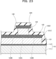
FIG. 23 is a cross-sectional view (part 7) illustrating the method for manufacturing the Josephson junction device according to the second embodiment. -
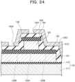
FIG. 24 is a cross-sectional view (part 8) illustrating the method for manufacturing the Josephson junction device according to the second embodiment. -
FIG. 25 is a cross-sectional view (part 9) illustrating the method for manufacturing the Josephson junction device according to the second embodiment. -
FIG. 26 is a cross-sectional view (part 10) illustrating the method for manufacturing the Josephson junction device according to the second embodiment. -
FIG. 27 is a diagram illustrating a quantum device according to a third embodiment. - Hereinafter, embodiments of the present disclosure will be specifically described with reference to the accompanying drawings. Note that, in the present description and the drawings, constituent elements having substantially the same functional configuration will be denoted by the same reference sign, and redundant explanation will sometimes not be made.
- First, a first embodiment is described. The first embodiment relates to a Josephson junction device.
FIG. 1 is a cross-sectional view illustrating a Josephson junction device according to the first embodiment.FIG. 2 is a plan view illustrating the Josephson junction device according to the first embodiment.FIG. 1 corresponds to a cross-sectional view taken along line I-I inFIG. 2 . InFIG. 2 , awire line 141, awire line 142, and aninsulating film 130 are omitted. - As illustrated in
FIGs. 1 and2 , a Josephsonjunction device 100 according to the first embodiment mainly includes asubstrate 110, asuperconducting film 121, aninsulating film 122, asuperconducting film 123, theinsulating film 130, thewire line 141, and thewire line 142. - The
substrate 110 includes, for example, a silicon (Si)substrate 111 and aninsulating film 112. Theinsulating film 112 is formed over thesilicon substrate 111. Theinsulating film 112 is, for example, a silicon oxide film. Thesubstrate 110 is a so-called oxide film-attached substrate. Thesuperconducting film 121 is provided over theinsulating film 112. Thesuperconducting film 121 is, for example, a niobium (Nb) film having a thickness of about 200 nm. The insulatingfilm 122 is provided over thesuperconducting film 121. The insulatingfilm 122 is, for example, an aluminum oxide (Al) film having a thickness of about 20 nm. Thesuperconducting film 123 is provided over the insulatingfilm 122. Thesuperconducting film 123 is, for example, a niobium film having a thickness of about 200 nm. Thesuperconducting film 121 is an example of a first superconducting film, the insulatingfilm 122 is an example of a first insulating film, and thesuperconducting film 123 is an example of a second superconducting film. - A surface layer portion of the insulating
film 122 includes afirst region 122A and asecond region 122B around thefirst region 122A. Greater damage has occurred in thesecond region 122B than thefirst region 122A, and the electrical insulation properties of thesecond region 122B are lower than the electrical insulation properties of thefirst region 122A. That is, the electrical insulation properties of thefirst region 122A are higher than the electrical insulation properties of thesecond region 122B. Thesuperconducting film 123 is provided over thefirst region 122A. In plan view, thesuperconducting film 123 is located at an inner side of a boundary betweenfirst region 122A andsecond region 122B. The magnitude of damage in thefirst region 122A and thesecond region 122B can be specified using, for example, a transmission electron microscope (TEM). In other words, in TEM observation, since the phase contrast is different between a region with great damage and a region with small damage, thefirst region 122A and thesecond region 122B can be distinguished from each other. - A
groove 121Z is formed in thesuperconducting film 121, and agroove 122Z is formed in the insulatingfilm 122. Thegroove 122Z communicates with thegroove 121Z, and the insulatingfilm 112 is exposed through thegrooves grooves film 130 covers thesubstrate 110, thesuperconducting film 121, the insulatingfilm 122, and thesuperconducting film 123. The insulatingfilm 130 is, for example, a silicon oxide film. - A
contact hole 122X is formed in the insulatingfilm 122, and acontact hole 130X is formed in the insulatingfilm 130. Thecontact hole 130X communicates with thecontact hole 122X, and thesuperconducting film 121 is exposed through thecontact holes contact hole 122X passes through thesecond region 122B, for example. Thewire line 141 is provided over the insulatingfilm 130 and also is in contact with thesuperconducting film 121 through thecontact holes wire line 141 is, for example, a niobium film. - A
contact hole 130Y is formed in the insulatingfilm 130. Thesuperconducting film 123 is exposed through thecontact hole 130Y. Arecess 123Y communicating with thecontact hole 130Y may be formed on a surface of thesuperconducting film 123. Thewire line 142 is provided over the insulatingfilm 130 and also is in contact with thesuperconducting film 123 through thecontact hole 130Y. Thewire line 142 is, for example, a niobium film. - Next, a method for manufacturing the
Josephson junction device 100 according to the first embodiment will be described.FIGs. 3 to 12 are cross-sectional views illustrating a method for manufacturing the Josephson junction device according to the first embodiment. - First, as illustrated in
FIG. 3 , thesubstrate 110 including thesilicon substrate 111 and the insulatingfilm 112 is prepared, and thesuperconducting film 121, the insulatingfilm 122, and thesuperconducting film 123 are formed over the insulatingfilm 112. - Next, as illustrated in
FIG. 4 , a resistpattern 191 is formed over thesuperconducting film 123. The resistpattern 191 includes anopening 191X. In plan view, theopening 191X approximately overlaps a region where thesecond region 122B of the insulatingfilm 122 is to be formed. - Thereafter, as illustrated in
FIG. 5 , thesuperconducting film 123 is etched with the resistpattern 191 as a mask. This etching is, for example, reactive ion etching (RIE) using areactive gas 150 containing sulfur hexafluoride (SF6) as a main component. This etching is performed until the insulatingfilm 122 is exposed. As a result, a portion of thesuperconducting film 123 covered with the resistpattern 191 remains. A vicinity of a side surface of the remainingsuperconducting film 123 is damaged by etching, and a damagedregion 123B is formed in the vicinity of the side surface of thesuperconducting film 123. Thesuperconducting film 123 has aninternal region 123A not damaged by etching on an inner side of the damagedregion 123B. In addition, a vicinity of an upper surface of the insulatingfilm 122 is also damaged by etching, and thefirst region 122A and thesecond region 122B around thefirst region 122A are formed in a surface layer portion of the insulatingfilm 122. In thesecond region 122B, etching damage greater than the etching damage in thefirst region 122A has occurred, and the electrical insulation properties of thesecond region 122B becomes lower than the electrical insulation properties of thefirst region 122A. Thefirst region 122A is formed at an inner side of an outer edge of the resistpattern 191 in plan view. - Subsequently, as illustrated in
FIG. 6 , the resistpattern 191 is removed. Next, the damagedregion 123B is removed by etching thesuperconducting film 123. This etching is, for example, isotropic etching such as wet etching. For example, thesuperconducting film 123 is etched by about 20 nm in a direction parallel to a surface of thesubstrate 110. That is, thesuperconducting film 123 is reduced in plan view by isotropic etching. As a result, thesuperconducting film 123 is positioned over thefirst region 122A and is positioned at an inner side of the boundary between thefirst region 122A and thesecond region 122B in plan view. In a case where the material of thesuperconducting film 123 is niobium, as the etchant, for example, a hydrogen fluoride (HF) solution, a mixed solution of HF and H2O2, a mixed solution of HF, H2SO4, and HNO3, or a mixed solution of HF and HNO3 can be used. In a case where the material of thesuperconducting film 123 is aluminum, for example, a diluted hydrochloric acid (HCl) solution or a diluted H2SO4 solution can be used as the etchant. - Thereafter, as illustrated in
FIG. 7 , a resistpattern 192 is formed over the insulatingfilm 122 and thesuperconducting film 123. The resistpattern 192 includes anopening 192Z. In plan view, theopening 192Z overlaps a region where thegrooves - Subsequently, as illustrated in
FIG. 8 , the insulatingfilm 122 is milled with the resistpattern 192 as a mask. As a result, thegroove 122Z is formed in the insulatingfilm 122. Furthermore, thesuperconducting film 123 is etched with the resistpattern 192 as a mask. This etching is, for example, RIE using a reactive gas containing sulfur hexafluoride as a main component. As a result, thegroove 121Z is formed in thesuperconducting film 121. - Next, as illustrated in
FIG. 9 , the resistpattern 192 is removed. Thereafter, the insulatingfilm 130 covering thesubstrate 110, thesuperconducting film 121, the insulatingfilm 122, and thesuperconducting film 123 is formed. The insulatingfilm 130 is formed by, for example, a chemical vapor deposition (CVD) method. - Subsequently, as illustrated in
FIG. 10 , a resistpattern 193 is formed over the insulatingfilm 130. The resistpattern 193 includesopenings opening 193X overlaps a region where thecontact holes opening 193Y overlaps a region where thecontact hole 130Y is to be formed. - Next, as illustrated in
FIG. 11 , the insulatingfilm 130 is etched with the resistpattern 193 as a mask. This etching is, for example, RIE using a reactive gas containing fluorocarbon (CF4) as a main component. As a result, thecontact holes film 130. Furthermore, the insulatingfilm 122 is milled with the resistpattern 193 as a mask. As a result, thecontact hole 130X is formed in the insulatingfilm 122. At this time, therecess 123Y may be formed in a portion of thesuperconducting film 123 exposed from thecontact hole 130Y. - Thereafter, as illustrated in
FIG. 12 , thewire line 141 in contact with thesuperconducting film 121 through thecontact holes wire line 142 in contact with thesuperconducting film 123 through thecontact hole 130Y are formed over the insulatingfilm 130. - In this manner, the
Josephson junction device 100 according to the first embodiment can be manufactured. Since the miniaturization of the Josephson junction device increases the proportion of a region of the superconducting film where damage has occurred, a change in properties is likely to become significant. Therefore, the present invention is particularly effective in such a case. - Here, effects obtained by the
Josephson junction device 100 according to the first embodiment will be described in comparison with a reference example.FIG. 13 is an enlarged cross-sectional view illustrating a part ofFIG. 1 .FIG. 14 is a cross-sectional view illustrating a portion corresponding to the Josephson junction device inFIG. 13 according to the reference example. - As illustrated in
FIG. 13 , thefirst region 122A and thesecond region 122B have been produced in the surface layer portion of the insulatingfilm 122, and damage due to the RIE (seeFIG. 5 ) has occurred in thesecond region 122B, whereas damage due to the RIE has not occurred in thefirst region 122A. That is, in thesecond region 122B, greater damage than damage in thefirst region 122A has occurred. Then, in the first embodiment, thesuperconducting film 123 is located at an inner side of the boundary between thefirst region 122A and thesecond region 122B in plan view. Therefore, aJosephson junction 100A between thesuperconducting film 121 and thesuperconducting film 123 is spaced from thesecond region 122B. Consequently, according to the first embodiment, stable properties may be obtained. - On the other hand, as illustrated in
FIG. 14 , in the reference example, thesuperconducting film 123 includes the damagedregion 123B, and thesuperconducting film 123 straddles the boundary between thefirst region 122A and thesecond region 122B and includes a portion outside this boundary in plan view. Between thesuperconducting film 121 and thesuperconducting film 123, there are not only theJosephson junction 100A spaced from thesecond region 122B, but also aJosephson junction 100B including thesecond region 122B. In addition, theJosephson junction 100B sometimes includes a Josephson junction between thesuperconducting film 121 and the damagedregion 123B. Accordingly, in the reference example, the properties are easy to vary. - Next, a second embodiment will be described. The second embodiment relates to a Josephson junction device.
FIG. 15 is a cross-sectional view illustrating a Josephson junction device according to the second embodiment.FIG. 16 is a plan view illustrating the Josephson junction device according to the second embodiment.FIG. 15 corresponds to a cross-sectional view taken along line XV-XV inFIG. 16 . InFIG. 16 , awire line 141, awire line 142, and an insulatingfilm 130 are omitted. - As illustrated in
FIGs. 15 and16 , aJosephson junction device 200 according to the second embodiment mainly includes asubstrate 110, asuperconducting film 121, an insulatingfilm 122, asuperconducting film 123, an insulatingfilm 224, the insulatingfilm 130, thewire line 141, and thewire line 142. - The insulating
film 224 is provided over thesuperconducting film 123. The insulatingfilm 224 is, for example, an aluminum oxide film having a thickness of about 20 nm. That is, the material of the insulatingfilm 224 is of the same type as the type of the material of the insulatingfilm 122, and a thickness of the insulatingfilm 224 is equal to a thickness of the insulatingfilm 122. The insulatingfilm 224 is an example of a second insulating film. - The insulating
film 130 covers thesubstrate 110, thesuperconducting film 121, the insulatingfilm 122, thesuperconducting film 123, and the insulatingfilm 224. The insulatingfilm 130 is an example of a third insulating film. - A
contact hole 122X is formed in the insulatingfilm 122, and acontact hole 130X is formed in the insulatingfilm 130. Thecontact hole 130X communicates with thecontact hole 122X, and thesuperconducting film 121 is exposed through thecontact holes contact hole 122X passes through asecond region 122B, for example. Thewire line 141 is provided over the insulatingfilm 130 and also is in contact with thesuperconducting film 121 through thecontact holes wire line 141 is an example of a first wire line. The contact holes 122X and 130X are examples of a first opening. - A
contact hole 224Y is formed in the insulatingfilm 224. Acontact hole 130Y communicates with thecontact hole 224Y, and thesuperconducting film 123 is exposed through thecontact holes recess 123Y is not formed on a surface of thesuperconducting film 123, and the surface of thesuperconducting film 123 is flat. Thewire line 142 is provided over the insulatingfilm 130 and also is in contact with thesuperconducting film 123 through thecontact holes wire line 142 is an example of a second wire line. The contact holes 224Y and 130Y are examples of a second opening. - Other constituent members are similar to those of the first embodiment.
- Next, a method for manufacturing the
Josephson junction device 200 according to the second embodiment will be described.FIGs. 17 to 26 are cross-sectional views illustrating a method for manufacturing the Josephson junction device according to the second embodiment. - First, as illustrated in
FIG. 17 , thesubstrate 110 including asilicon substrate 111 and an insulatingfilm 112 is prepared, and thesuperconducting film 121, the insulatingfilm 122, thesuperconducting film 123, and the insulatingfilm 224 are formed over the insulatingfilm 112. - Next, as illustrated in
FIG. 18 , a resistpattern 191 is formed over the insulatingfilm 224. The resistpattern 191 includes anopening 191X. In plan view, theopening 191X approximately overlaps a region where thesecond region 122B of the insulatingfilm 122 is to be formed. - Thereafter, as illustrated in
FIG. 19 , the insulatingfilm 224 is milled with the resistpattern 191 as a mask. Furthermore, similarly to the first embodiment, thesuperconducting film 123 is etched. As a result, a damagedregion 123B is formed in the vicinity of a side surface of thesuperconducting film 123. Thesuperconducting film 123 has aninternal region 123A not damaged by etching on an inner side of the damagedregion 123B. In addition, afirst region 122A and thesecond region 122B around thefirst region 122A are formed in a surface layer portion of the insulatingfilm 122. - Subsequently, as illustrated in
FIG. 20 , the resistpattern 191 is removed. Next, similarly to the first embodiment, isotropic etching for thesuperconducting film 123 is performed to remove the damagedregion 123B. That is, thesuperconducting film 123 is reduced in plan view by isotropic etching. As a result, thesuperconducting film 123 is positioned over thefirst region 122A and is positioned at an inner side of the boundary between thefirst region 122A and thesecond region 122B in plan view. - Thereafter, as illustrated in
FIG. 21 , a resistpattern 192 is formed over the insulatingfilm 122, thesuperconducting film 123, and the insulatingfilm 224. The resistpattern 192 includes anopening 192Z. In plan view, theopening 192Z overlaps a region wheregrooves - Subsequently, as illustrated in
FIG. 22 , the insulatingfilm 122 is milled with the resistpattern 192 as a mask, similarly to the first embodiment. As a result, thegroove 122Z is formed in the insulatingfilm 122. Furthermore, similarly to the first embodiment, thesuperconducting film 123 is etched with the resistpattern 192 as a mask. As a result, thegroove 121Z is formed in thesuperconducting film 121. - Next, as illustrated in
FIG. 23 , the resistpattern 192 is removed. Thereafter, the insulatingfilm 130 covering thesubstrate 110, thesuperconducting film 121, the insulatingfilm 122, thesuperconducting film 123, and the insulatingfilm 224 is formed. The insulatingfilm 130 is formed by, for example, the CVD method. - Subsequently, as illustrated in
FIG. 24 , a resistpattern 193 is formed over the insulatingfilm 130, similarly to the first embodiment. The resistpattern 193 includesopenings opening 193X overlaps a region where thecontact holes opening 193Y overlaps a region where thecontact holes - Next, as illustrated in
FIG. 25 , the insulatingfilm 130 is etched with the resistpattern 193 as a mask, similarly to the first embodiment. As a result, thecontact holes film 130. Furthermore, the insulatingfilms pattern 193 as a mask. As a result, thecontact hole 130X is formed in the insulatingfilm 122, and thecontact hole 130Y is formed in the insulatingfilm 224. Since the material of the insulatingfilm 224 is of the same type as the type of the material of the insulatingfilm 122 and a thickness of the insulatingfilm 224 is equal to a thickness of the insulatingfilm 122, if the milling of the insulatingfilm 122 is stopped when thesuperconducting film 121 is exposed, the milling of the insulatingfilm 224 is also stopped when thesuperconducting film 123 is exposed. - Thereafter, as illustrated in
FIG. 26 , thewire line 141 in contact with thesuperconducting film 121 through thecontact holes wire line 142 in contact with thesuperconducting film 123 through thecontact holes film 130. - In this manner, the
Josephson junction device 200 according to the second embodiment can be manufactured. - Effects similar to those of the first embodiment may also be exerted by the second embodiment. In addition, in the second embodiment, formation of the
recess 123Y on the surface of thesuperconducting film 123 can be suppressed. Accordingly, damage to thesuperconducting film 123 caused by formation of therecess 123Y may be suppressed. - Note that a thickness of the insulating
film 224 preferably coincides with a thickness of the insulatingfilm 122, but the insulatingfilm 224 may be thicker or thinner than the insulatingfilm 122. In addition, the material of the insulatingfilm 224 is preferably of the same type as the type of the material of the insulatingfilm 122, but does not necessarily have to be the same. In any case, it is desirable that deviation of end timings is small between the milling of the insulatingfilm 224 and the milling of the insulatingfilm 122. - The material of the
superconducting films films - Next, a third embodiment will be described. The third embodiment relates to a quantum device.
FIG. 27 is a diagram illustrating a quantum device according to the third embodiment. - A
quantum device 300 according to the third embodiment includes aqubit 310, aread circuit 320, andwire lines qubit 310 includesJosephson junction devices read circuit 320 includesJosephson junction devices read circuit 320 is coupled between thewire lines qubit 310 is provided at an inner side of the readcircuit 320. Theread circuit 320 reads the state of thequbit 310. TheJosephson junction devices Josephson junction device - Since the
quantum device 300 according to the third embodiment includes theJosephson junction device quantum device 300 can be used for, for example, a quantum computer. - Although the preferred embodiments and the like have been described in detail so far, the embodiments are not restricted to the above-described embodiments and the like, and various modifications and substitutions can be made to the embodiments and the like described above, without departing from the scope disclosed in the claims.
-
- 100, 200, 311, 312, 313, 321, 322 Josephson junction device
- 121, 123 Superconducting film
- 122, 130, 224 Insulating film
- 122A First region
- 122B Second region
- 123A Internal region
- 123B Damaged region
- 123Y Recess
- 122X, 130X, 130Y, 224Y Contact hole
- 141, 142 Wire line
- 300 Quantum device
- 310 Qubit
- 320 Read circuit
Claims (14)
- A Josephson junction device comprising:a first superconducting film;a first insulating film provided over the first superconducting film; anda second superconducting film provided over the first insulating film, whereina surface layer portion of the first insulating film includes:a first region; anda second region around the first region,electrical insulation properties of the first region are higher than the electrical insulation properties of the second region, andthe second superconducting film is located at an inner side of a boundary between the first region and the second region in plan view.
- The Josephson junction device according to claim 1, comprising:a second insulating film provided over the second superconducting film; anda third insulating film that covers the first insulating film, the second superconducting film, and the second insulating film, whereina first opening that reaches the first superconducting film is formed in the first insulating film and the third insulating film,a second opening that reaches the second superconducting film is formed in the second insulating film and the third insulating film, andthe Josephson junction device comprises: a first wire line coupled to the first superconducting film through the first opening; anda second wire line coupled to the second superconducting film through the second opening.
- The Josephson junction device according to claim 2, wherein materials of the second insulating film are of same types as the types of the materials of the first insulating film, and
a thickness of the second insulating film is equal to the thickness of the first insulating film. - The Josephson junction device according to claim 2 or 3, wherein the second superconducting film is located at an inner side of an outer edge of the second insulating film in plan view.
- The Josephson junction device according to any one of claims 1 to 3, wherein materials of the first insulating film include aluminum oxide, aluminum nitride, hafnium oxide, or yttrium oxide, or any combination of the aluminum oxide, the aluminum nitride, the hafnium oxide, and the yttrium oxide.
- The Josephson junction device according to any one of claims 1 to 3, wherein materials of the first superconducting film and the second superconducting film include niobium, aluminum, niobium nitride, or titanium nitride, or any combination of the niobium, the aluminum, the niobium nitride, and the titanium nitride.
- A quantum device comprising:
a Josephson junction device including:a first superconducting film;a first insulating film provided over the first superconducting film; anda second superconducting film provided over the first insulating film, whereina surface layer portion of the first insulating film includes:a first region; anda second region around the first region,electrical insulation properties of the first region are higher than the electrical insulation properties of the second region, andthe second superconducting film is located at an inner side of a boundary between the first region and the second region in plan view. - The quantum device according to claim 7, comprising:a second insulating film provided over the second superconducting film; anda third insulating film that covers the first insulating film, the second superconducting film, and the second insulating film, whereina first opening that reaches the first superconducting film is formed in the first insulating film and the third insulating film,a second opening that reaches the second superconducting film is formed in the second insulating film and the third insulating film, andthe Josephson junction device comprises: a first wire line coupled to the first superconducting film through the first opening; anda second wire line coupled to the second superconducting film through the second opening.
- The quantum device according to claim 8, wherein materials of the second insulating film are of same types as the types of the materials of the first insulating film, and
a thickness of the second insulating film is equal to the thickness of the first insulating film. - The quantum device according to claim 8 or 9, wherein the second superconducting film is located at an inner side of an outer edge of the second insulating film in plan view.
- The quantum device according to any one of claims 7 to 9, wherein materials of the first insulating film include aluminum oxide, aluminum nitride, hafnium oxide, or yttrium oxide, or any combination of the aluminum oxide, the aluminum nitride, the hafnium oxide, and the yttrium oxide.
- The quantum device according to any one of claims 7 to 9, wherein materials of the first superconducting film and the second superconducting film include niobium, aluminum, niobium nitride, or titanium nitride, or any combination of the niobium, the aluminum, the niobium nitride, and the titanium nitride.
- A method for manufacturing a Josephson junction device, comprising:providing a first insulating film over a first superconducting film;providing a second superconducting film over the first insulating film;processing the second superconducting film by reactive ion etching; andetching a sidewall of the processed second superconducting film.
- The method for manufacturing the Josephson junction device according to claim 13, comprising:between the providing the second superconducting film and the processing the second superconducting film,providing a second insulating film over the second superconducting film; andprocessing the second insulating film, and
comprising:after the etching the sidewall of the second superconducting film,providing a third insulating film that covers the first insulating film, the second superconducting film, and the second insulating film;forming a first opening that reaches the first superconducting film, in the first insulating film and the third insulating film, and forming a second opening that reaches the second superconducting film, in the second insulating film and the third insulating film; andproviding a first wire line coupled to the first superconducting film through the first opening, and a second wire line coupled to the second superconducting film through the second opening.
Applications Claiming Priority (1)
| Application Number | Priority Date | Filing Date | Title |
|---|---|---|---|
| PCT/JP2022/017665 WO2023199419A1 (en) | 2022-04-13 | 2022-04-13 | Josephson junction element, quantum device, and production method for josephson junction element |
Publications (2)
| Publication Number | Publication Date |
|---|---|
| EP4510170A1 true EP4510170A1 (en) | 2025-02-19 |
| EP4510170A4 EP4510170A4 (en) | 2025-09-24 |
Family
ID=88329252
Family Applications (1)
| Application Number | Title | Priority Date | Filing Date |
|---|---|---|---|
| EP22937398.0A Pending EP4510170A4 (en) | 2022-04-13 | 2022-04-13 | Josephson transition element, quantum device, and manufacturing method for a Josephson transition element |
Country Status (3)
| Country | Link |
|---|---|
| EP (1) | EP4510170A4 (en) |
| JP (1) | JPWO2023199419A1 (en) |
| WO (1) | WO2023199419A1 (en) |
Family Cites Families (12)
| Publication number | Priority date | Publication date | Assignee | Title |
|---|---|---|---|---|
| JPS62213287A (en) | 1986-03-14 | 1987-09-19 | Agency Of Ind Science & Technol | Manufacturing method of Josephson device |
| JPS6396973A (en) * | 1986-10-14 | 1988-04-27 | Fujitsu Ltd | Manufacture of josephson junction element |
| EP0476844A1 (en) | 1990-09-21 | 1992-03-25 | Trw Inc. | Method for fabricating Josephson tunnel junctions with accurate junction area control |
| JPH04188683A (en) * | 1990-11-19 | 1992-07-07 | Sanyo Electric Co Ltd | Planar tunnel Josephson device and its manufacturing method |
| US5625290A (en) * | 1994-02-23 | 1997-04-29 | Micontech, Inc. | Complex superconducting quantum interference device and circuit |
| JP2003218413A (en) * | 2002-01-22 | 2003-07-31 | National Institute Of Advanced Industrial & Technology | Superconducting radiation detector and manufacturing method thereof |
| US7060508B2 (en) * | 2003-02-12 | 2006-06-13 | Northrop Grumman Corporation | Self-aligned junction passivation for superconductor integrated circuit |
| US7615385B2 (en) | 2006-09-20 | 2009-11-10 | Hypres, Inc | Double-masking technique for increasing fabrication yield in superconducting electronics |
| JP5207271B2 (en) * | 2007-09-05 | 2013-06-12 | 独立行政法人物質・材料研究機構 | In-plane Josephson junction formation on high-temperature superconducting single crystals. |
| JP5801676B2 (en) * | 2011-10-04 | 2015-10-28 | 東京エレクトロン株式会社 | Manufacturing method of semiconductor device |
| US9355362B2 (en) | 2011-11-11 | 2016-05-31 | Northrop Grumman Systems Corporation | Quantum bits and method of forming the same |
| US9634224B2 (en) * | 2014-02-14 | 2017-04-25 | D-Wave Systems Inc. | Systems and methods for fabrication of superconducting circuits |
-
2022
- 2022-04-13 JP JP2024515226A patent/JPWO2023199419A1/ja active Pending
- 2022-04-13 EP EP22937398.0A patent/EP4510170A4/en active Pending
- 2022-04-13 WO PCT/JP2022/017665 patent/WO2023199419A1/en not_active Ceased
Also Published As
| Publication number | Publication date |
|---|---|
| WO2023199419A1 (en) | 2023-10-19 |
| JPWO2023199419A1 (en) | 2023-10-19 |
| EP4510170A4 (en) | 2025-09-24 |
Similar Documents
| Publication | Publication Date | Title |
|---|---|---|
| US6784077B1 (en) | Shallow trench isolation process | |
| US20090315021A1 (en) | Double-masking technique for increasing fabrication yield in superconducting electronics | |
| JP5105824B2 (en) | Method for forming mask structure and method for forming fine pattern using the same | |
| US20230163161A1 (en) | Metal insulator metal (mim) structure and manufacturing method thereof | |
| KR100270464B1 (en) | Method of forming recessed oxide isolation | |
| TWI859495B (en) | Superconducting device and methods for manufacturing a superconducting device | |
| US12211699B2 (en) | Method of removing step height on gate structure | |
| CN1956153A (en) | Method of forming a trench semiconductor device and structure therefor | |
| EP0743678A1 (en) | Planar isolation in integrated circuits | |
| WO2023199419A1 (en) | Josephson junction element, quantum device, and production method for josephson junction element | |
| US20240321779A1 (en) | Interconnection member and method of manufacturing the same | |
| EP4598330A1 (en) | Quantum device, quantum computer, and method for manufacturing quantum device | |
| CN108807267B (en) | Semiconductor device and method of manufacturing the same | |
| JP2757919B2 (en) | Method for manufacturing semiconductor device | |
| EP3330800B1 (en) | A photomask manufacturing method | |
| KR100303225B1 (en) | Semiconductor device and method of producing the same | |
| JP3571236B2 (en) | Method for manufacturing semiconductor device | |
| CN113764339B (en) | Semiconductor structure and method of forming the same | |
| US10607848B2 (en) | Method of fabricating semiconductor device | |
| JPH07183315A (en) | Semiconductor device and method of manufacturing semiconductor device | |
| EP4694659A1 (en) | Method of manufacturing quantum device and quantum device | |
| US10276563B2 (en) | Semiconductor devices and methods for forming the same | |
| US12439677B2 (en) | Method for manufacturing semiconductor device, and semiconductor device | |
| US20020093066A1 (en) | Method for forming a gate of a high integration semiconductor device | |
| CN118231238A (en) | Shallow trench sidewall and forming method |
Legal Events
| Date | Code | Title | Description |
|---|---|---|---|
| STAA | Information on the status of an ep patent application or granted ep patent |
Free format text: STATUS: THE INTERNATIONAL PUBLICATION HAS BEEN MADE |
|
| PUAI | Public reference made under article 153(3) epc to a published international application that has entered the european phase |
Free format text: ORIGINAL CODE: 0009012 |
|
| STAA | Information on the status of an ep patent application or granted ep patent |
Free format text: STATUS: REQUEST FOR EXAMINATION WAS MADE |
|
| 17P | Request for examination filed |
Effective date: 20240903 |
|
| AK | Designated contracting states |
Kind code of ref document: A1 Designated state(s): AL AT BE BG CH CY CZ DE DK EE ES FI FR GB GR HR HU IE IS IT LI LT LU LV MC MK MT NL NO PL PT RO RS SE SI SK SM TR |
|
| REG | Reference to a national code |
Ref country code: DE Ref legal event code: R079 Free format text: PREVIOUS MAIN CLASS: H99Z9999999999 Ipc: H10N0060010000 |
|
| RIC1 | Information provided on ipc code assigned before grant |
Ipc: H10N 60/12 20230101ALI20250415BHEP Ipc: H10N 60/01 20230101AFI20250415BHEP |
|
| DAV | Request for validation of the european patent (deleted) | ||
| DAX | Request for extension of the european patent (deleted) | ||
| A4 | Supplementary search report drawn up and despatched |
Effective date: 20250825 |
|
| RIC1 | Information provided on ipc code assigned before grant |
Ipc: H10N 60/01 20230101AFI20250819BHEP Ipc: H10N 60/12 20230101ALI20250819BHEP |