EP4507202A1 - All-digital phase-locked loop circuit - Google Patents
All-digital phase-locked loop circuit Download PDFInfo
- Publication number
- EP4507202A1 EP4507202A1 EP23784619.1A EP23784619A EP4507202A1 EP 4507202 A1 EP4507202 A1 EP 4507202A1 EP 23784619 A EP23784619 A EP 23784619A EP 4507202 A1 EP4507202 A1 EP 4507202A1
- Authority
- EP
- European Patent Office
- Prior art keywords
- output
- tdc
- time
- digital converter
- phase
- Prior art date
- Legal status (The legal status is an assumption and is not a legal conclusion. Google has not performed a legal analysis and makes no representation as to the accuracy of the status listed.)
- Pending
Links
Images








Classifications
-
- H—ELECTRICITY
- H03—ELECTRONIC CIRCUITRY
- H03L—AUTOMATIC CONTROL, STARTING, SYNCHRONISATION OR STABILISATION OF GENERATORS OF ELECTRONIC OSCILLATIONS OR PULSES
- H03L7/00—Automatic control of frequency or phase; Synchronisation
- H03L7/06—Automatic control of frequency or phase; Synchronisation using a reference signal applied to a frequency- or phase-locked loop
- H03L7/08—Details of the phase-locked loop
- H03L7/085—Details of the phase-locked loop concerning mainly the frequency- or phase-detection arrangement including the filtering or amplification of its output signal
-
- H—ELECTRICITY
- H03—ELECTRONIC CIRCUITRY
- H03L—AUTOMATIC CONTROL, STARTING, SYNCHRONISATION OR STABILISATION OF GENERATORS OF ELECTRONIC OSCILLATIONS OR PULSES
- H03L7/00—Automatic control of frequency or phase; Synchronisation
- H03L7/06—Automatic control of frequency or phase; Synchronisation using a reference signal applied to a frequency- or phase-locked loop
- H03L7/08—Details of the phase-locked loop
- H03L7/085—Details of the phase-locked loop concerning mainly the frequency- or phase-detection arrangement including the filtering or amplification of its output signal
- H03L7/087—Details of the phase-locked loop concerning mainly the frequency- or phase-detection arrangement including the filtering or amplification of its output signal using at least two phase detectors or a frequency and phase detector in the loop
-
- H—ELECTRICITY
- H03—ELECTRONIC CIRCUITRY
- H03L—AUTOMATIC CONTROL, STARTING, SYNCHRONISATION OR STABILISATION OF GENERATORS OF ELECTRONIC OSCILLATIONS OR PULSES
- H03L7/00—Automatic control of frequency or phase; Synchronisation
- H03L7/06—Automatic control of frequency or phase; Synchronisation using a reference signal applied to a frequency- or phase-locked loop
- H03L7/08—Details of the phase-locked loop
- H03L7/0802—Details of the phase-locked loop the loop being adapted for reducing power consumption
-
- H—ELECTRICITY
- H03—ELECTRONIC CIRCUITRY
- H03L—AUTOMATIC CONTROL, STARTING, SYNCHRONISATION OR STABILISATION OF GENERATORS OF ELECTRONIC OSCILLATIONS OR PULSES
- H03L7/00—Automatic control of frequency or phase; Synchronisation
- H03L7/06—Automatic control of frequency or phase; Synchronisation using a reference signal applied to a frequency- or phase-locked loop
- H03L7/08—Details of the phase-locked loop
- H03L7/099—Details of the phase-locked loop concerning mainly the controlled oscillator of the loop
- H03L7/0991—Details of the phase-locked loop concerning mainly the controlled oscillator of the loop the oscillator being a digital oscillator, e.g. composed of a fixed oscillator followed by a variable frequency divider
-
- H—ELECTRICITY
- H03—ELECTRONIC CIRCUITRY
- H03L—AUTOMATIC CONTROL, STARTING, SYNCHRONISATION OR STABILISATION OF GENERATORS OF ELECTRONIC OSCILLATIONS OR PULSES
- H03L7/00—Automatic control of frequency or phase; Synchronisation
- H03L7/06—Automatic control of frequency or phase; Synchronisation using a reference signal applied to a frequency- or phase-locked loop
- H03L7/16—Indirect frequency synthesis, i.e. generating a desired one of a number of predetermined frequencies using a frequency- or phase-locked loop
- H03L7/18—Indirect frequency synthesis, i.e. generating a desired one of a number of predetermined frequencies using a frequency- or phase-locked loop using a frequency divider or counter in the loop
- H03L7/197—Indirect frequency synthesis, i.e. generating a desired one of a number of predetermined frequencies using a frequency- or phase-locked loop using a frequency divider or counter in the loop a time difference being used for locking the loop, the counter counting between numbers which are variable in time or the frequency divider dividing by a factor variable in time, e.g. for obtaining fractional frequency division
-
- H—ELECTRICITY
- H03—ELECTRONIC CIRCUITRY
- H03L—AUTOMATIC CONTROL, STARTING, SYNCHRONISATION OR STABILISATION OF GENERATORS OF ELECTRONIC OSCILLATIONS OR PULSES
- H03L2207/00—Indexing scheme relating to automatic control of frequency or phase and to synchronisation
- H03L2207/50—All digital phase-locked loop
Definitions
- the present disclosure relates to an all digital phase-locked loop circuit, and in particular to an all digital phase-locked loop circuit that can be more easily designed.
- ADPLL all digital PLL circuit in which all components of a phase locked loop (PLL) circuit are digitized.
- the ADPLL circuit has a configuration in which a time to digital converter (TDC) is used to extract phase difference information of an output of a digitally controlled oscillator (DCO) that controls a frequency by digital control.
- TDC time to digital converter
- DCO digitally controlled oscillator
- Patent Documents 1 and 2 disclose configurations disclosed in Patent Documents 1 and 2.
- Patent Document 3 discloses a configuration of a TDC applicable to an ADPLL circuit.
- the present disclosure has been made in view of such a situation, and an object of the present disclosure is to enable design more easily.
- An all digital phase-locked loop circuit includes: a first time-to-digital converter that performs phase difference detection at a first resolution; and a second time-to-digital converter that performs phase difference detection at a second resolution finer than the first resolution and that is arranged in parallel with the first time-to-digital converter, in which the second time-to-digital converter is configured to allow being disabled, and the first time-to-digital converter outputs a clock synchronization selection signal used for synchronizing a reference clock signal to a clock synchronization unit that generates a clock signal of a digital part.
- a first time-to-digital converter that performs phase difference detection at a first resolution and a second time-to-digital converter that performs phase difference detection at a second resolution finer than the first resolution are arranged in parallel, in which the second time-to-digital converter is configured to allow being disabled, and the first time-to-digital converter outputs a clock synchronization selection signal used for synchronizing a reference clock signal to a clock synchronization unit that generates a clock signal of a digital part.
- all digital phase-locked loop circuit may be an independent device or an internal block configuring one device.
- Fig. 1 is a block diagram illustrating a configuration example of an embodiment of an ADPLL circuit to which the present disclosure is applied.
- An ADPLL circuit 10 is an all digital phase-locked loop circuit that generates an output from a DCO that controls a frequency by digital control, from a digital frequency control input (frequency command word (FCW)) and a reference frequency input (reference clock signal: REFCLK) from the outside, adjusts the DCO on the basis of a difference from the FCW obtained from the output signal, and performs an operation of adjusting the output to a control value by the FCW based on the reference frequency input.
- FCW frequency command word
- REFCLK reference clock signal
- the ADPLL circuit 10 includes a control unit 100, an REF accumulator 101, an adder 102, a loop filter 103, an OTW IF 104, a DCO 105, a frequency divider 106, a TDC 107, a clock synchronization unit 108, and an accumulator 109.
- the control unit 100 controls the operation of each unit of the ADPLL circuit 10.
- the DCO 105 is a digitally controlled oscillator that outputs a signal having an oscillation frequency indicated by an oscillator control word (oscillator tuning word (OTW)) input from the OTW IF 104.
- An output signal output from the DCO 105 is an output (clock signal: CLK) of the ADPLL circuit 10.
- the frequency divider 106 frequency-divides an output signal from the DCO 105 at a predetermined frequency division ratio, and outputs the signal to the TDC 107 as a frequency-divided output signal (VCLK).
- VCLK frequency-divided output signal
- the frequency divider 106 is provided as necessary, and in a case where the frequency divider 106 is not provided, the output signal from the DCO 105 is directly input to the TDC 107 as VCLK. In the following description, a case where the frequency divider 106 is provided as illustrated in Fig. 1 and VCLK from the frequency divider 106 is input to the TDC 107 will be described.
- the TDC 107 is a time-to-digital converter that detects phase difference information of an output signal of the DCO 105 from REFCLK input as a reference clock signal and VCLK input from the frequency divider 106.
- the TDC 107 outputs the phase difference information to the adder 102.
- the TDC 107 outputs a VCLK_DIV obtained by dividing VCLK at a predetermined frequency division ratio to the clock synchronization unit 108 and the accumulator 109.
- the TDC 107 outputs a clock synchronization selection signal (hereinafter, also referred to as a sel edge signal) used for synchronizing REFCLK with VCLK_DIV to the clock synchronization unit 108. Furthermore, an enable signal (hereinafter, also referred to as a fine TDC EN signal) and an output selection signal (hereinafter, also referred to as a PHF sel signal) are input to the TDC 107 under the control of the control unit 100. Details of the configuration of the TDC 107 will be described later with reference to Fig. 2 .
- the clock synchronization unit 108 generates RTREFCLK by synchronizing REFCLK input as a reference clock signal using the sel edge signal and VCLK_DIV input from the TDC 107, and outputs RTREFCLK to each unit.
- the RTREFCLK is a clock signal of the digital part of the ADPLL circuit 10.
- the accumulator 109 functions as a counter that accumulates a predetermined value (for example, 1) in synchronization with VCLK_DIV input from the TDC 107, and outputs the accumulated value to the adder 102.
- the REF accumulator 101 inputs phase control information obtained from FCW input thereto to the adder 102.
- the adder 102 adds the output (accumulated value as an integer part) from the accumulator 109 and the output (phase difference information as a decimal part) from the TDC 107 to obtain phase information. Furthermore, the adder 102 subtracts the phase information obtained by the addition from the phase control information input from the REF accumulator 101 to generate phase error information, and outputs the phase error information to the loop filter 103.
- the loop filter 103 performs filter processing on the phase error information input from the adder 102, generates a control value for the DCO 105, and outputs the control value to the OTW IF 104.
- the OTW IF 104 generates OTW on the basis of the control value input from the loop filter 103 and outputs OTW to the DCO 105.
- the oscillation frequency of the DCO 105 is controlled by repeating the above-described operation.
- Fig. 2 is a block diagram illustrating an example configuration of the TDC 107 illustrated in Fig. 1 .
- the TDC 107 includes an N frequency divider 131, a coarse TDC 132, a fine TDC 133, and an output generation unit 135.
- the fine TDC 133 includes a fine TDC main circuit 133A and a 1/N multiplier 134.
- a coarse TDC 132 and a fine TDC 133 are provided in parallel.
- the coarse TDC 132 performs phase difference detection at a first resolution.
- the fine TDC 133 performs phase difference detection at a second resolution finer than the first resolution.
- the fine TDC 133 can be disabled by the fine TDC EN signal.
- the coarse TDC 132 outputs the sel edge signal to the clock synchronization unit 108.
- the fine TDC 133 is disabled and only the coarse TDC 132 can be used to achieve a low power consumption operation.
- the fine TDC 133 is enabled and the coarse TDC 132 and the fine TDC 133 can be combined to achieve a high resolution operation.
- a clock skew time difference of clocks
- the sel edge signal generated on the basis of the phase difference information (phase difference information between REFCLK and VCLK_DIV) measured by the TDC 107 (coarse TDC 132) is transmitted to the clock synchronization unit 108, and in response, the clock synchronization unit 108 selects a VCLK_DIV edge to synchronize REFCLK.
- the sel edge signal is a signal indicating which of the rise and fall of VCLK_DIV is farther from REFCLK edge.
- the phase relationship between REFCLK and VCLK_DIV and the phase relationship with the coarse TDC 132 need to be the same, and thus minimization of the clock skew is required.
- the coarse TDC 132 having a coarse resolution and a small size can be arranged (physically) close to the clock synchronization unit 108 in the TDC 107, and the clock skew can be minimized.
- the TDC 107 can realize the operation mode switching function of performing the low power consumption operation using only the coarse TDC 132 in a case where a bad jitter is allowed, and performing the high resolution operation with the fine TDC 133 when a low jitter is required. Furthermore, in the TDC 107, the sel edge signal is output from the coarse TDC 132, which is easily downsized, so that a clock skew design that matches the clock synchronization unit 108 is facilitated.
- the output generation unit 135 outputs phase difference information (PHF) on the basis of the output of the coarse TDC 132 (PHF1), the output of the fine TDC 133 (PHF2), and the PHF sel signal.
- PHF phase difference information
- the fine TDC 133 is disabled, the phase difference information (PHF) is output on the basis of the output (PHF1) of the coarse TDC 132.
- the fine TDC 133 is enabled, the phase difference information (PHF) is output on the basis of the output (PHF1) of the coarse TDC 132, the output (PHF2) of the fine TDC 133, and the PHF sel.
- the output generation unit 135 outputs a combination of these TDC outputs.
- the output of the coarse TDC 132 is output as it is (or may be delayed).
- the output of the coarse TDC 132 can be output as it is or a value generated by combining the outputs of the coarse TDC 132 and the fine TDC 133 can be output on the basis of the PHF sel signal.
- the fine TDC 133 typically performs averaging processing to obtain the period of VCLK therein, and may output an instable value immediately after being enabled. Therefore, by controlling the output generation unit 135 using the PHF sel signal different from the fine TDC EN signal of the fine TDC 133, propagation of the instable value to subsequent stages, and then malfunction of the ADPLL circuit 10 can be prevented. Furthermore, the fine TDC 133 is enabled in advance, and the PHF sel signal is switched at a necessary timing after stabilization, whereby seamless operation mode switching can be realized.
- the output generation unit 135 can generate phase difference information by combining the output of the coarse TDC 132 and the output of the fine TDC 133. Furthermore, the output generation unit 135 performs output on the basis of the PHF sel signal different from the fine TDC EN signal of the fine TDC 133, so that it is possible to avoid the influence of the unstable operation immediately after enabling the fine TDC 133 on the loop operation and realize seamless operation mode switching.
- the N frequency divider 131 is provided for a VCLK input common to the coarse TDC 132, the clock synchronization unit 108, and the accumulator 109.
- N is an integer.
- the resolution of the coarse TDC 132 converted for the output needs to be finer than 1/N. That is, since the output conversion measurement range (hereinafter, also referred to as a measurement range) of the fine TDC 133 is 1/N and the measurement range converted for input of the fine TDC 133 matches the VCLK period, the resolution of the coarse TDC 132 is finer than VCLK period.
- the input conversion measurement range is assumed to match the period of the high-speed clock input (VCLK). Furthermore, it is assumed that the output of the TDC 107 is obtained by normalizing the time difference between REFCLK and VCLK by the period of the high-speed clock input (VCLK). That is, the output of the TDC 107 is in the range of 0 to 1.
- the denominator of normalization becomes N times
- the input range increases by N times
- the output value becomes 1/N times those in a case where the N frequency divider 131 is not provided, although the time difference is the same.
- the 1/N multiplier 134 is arranged at the subsequent stage of the fine TDC main circuit 133A that performs phase difference detection in order to match the input time difference with the relationship between the output values between the coarse TDC 132 and the fine TDC 133 in consideration of the change in the output of the coarse TDC 132 by the N frequency divider 131.
- the slow clock operation due to the N frequency divider 131 can reduce the power consumption of the coarse TDC 132, the clock synchronization unit 108, and the accumulator 109. Moreover, by restricting the resolution of the coarse TDC 132, the information of the coarse TDC 132 can be interpolated with the information of the fine TDC 133, and the phase difference information can be correctly obtained without missing any information.
- the output generation unit 135 includes a selector 151, a nearest neighbor correction unit 152, an adder 153, and an adder 154.
- the adder 153 adds a value (hereinafter, also referred to as a skew estimation value) corresponding to the skew between the coarse TDC 132 and the fine TDC 133 to the output of the fine TDC 133.
- a skew estimation value a value corresponding to the skew between the coarse TDC 132 and the fine TDC 133 to the output of the fine TDC 133.
- the selector 151 selects, on the basis of the PHF sel signal, the output of the coarse TDC 132 or the output generated on the basis of the output of the coarse TDC 132 and the output of the fine TDC 133, and outputs the selected output as phase difference information (PHF).
- the control unit 100 independently controls the fine TDC EN signal input to the fine TDC 133 and the PHF sel signal input to the selector 151.
- the TDC 107 is configured as described above. With this configuration, for example, the following effects can be obtained. That is, since the coarse TDC 132 and the fine TDC 133 that can be disabled are provided in parallel, it is possible to provide the operation mode switching function of performing the low power consumption operation using only the coarse TDC 132 in a case where a bad jitter is allowed, and performing the high resolution operation in which the coarse TDC 132 and the fine TDC 133 are combined when a low jitter is required. Furthermore, the sel edge signal is output from the coarse TDC 132, which is easily downsized, so that a skew design that matches the clock synchronization unit 108 can be easily realized.
- the power consumption of the coarse TDC 132, the clock synchronization unit 108, and the accumulator 109 is reduced by the slow clock operation due to the N frequency divider 131 while the information of the fine TDC 133 is interpolated in the information of the coarse TDC 132, so that the phase difference information can be correctly obtained without missing any information.
- a 2 frequency divider is used as the N frequency divider 131, and the resolution of the coarse TDC 132 converted for the output is set to 0.25.
- values stated herein are values normalized by one period of VCLK_DIV.
- Fig. 3 is a timing chart illustrating an operation example of the coarse TDC 132 and the fine TDC 133 of Fig. 2 .
- a of Fig. 3 illustrates a relationship between the TDC input timing chart and the measurement edge.
- VCLK_DIV and REFCLK are signals input to the coarse TDC 132
- VCLK_fine and REFCLK_fine are signals input to the fine TDC 133.
- the coarse TDC 132 measures the time from the rise of REFCLK to the rise of VCLK_DIV.
- the fine TDC 133 measures the time from the rise of REFCLK_fine (here, the same signal as REFCLK) to the rise of VCLK_fine.
- REFCLK (REFCLK_fine) rises at a position of 0.9 for the coarse TDC 132 and at a position of 0.4 for the fine TDC 133.
- Each of the coarse TDC 132 and the fine TDC 133 measures time corresponding to the rise timing.
- the output values are values obtained by rounding down by intervals determined by the resolutions.
- B of Fig. 3 illustrates the relationship between the rise timings of REFCLK and the TDC output.
- the horizontal axis represents the rising timing of REFCLK
- the vertical axis represents the output value of each TDC.
- the coarse TDC 132 is output in a coarse stepwise manner corresponding to the resolution 0.25.
- the fine TDC 133 has a fine resolution, and thus is output substantially linearly.
- the fine TDC 133 has an output conversion measurement range of 1/N, and when the output value exceeds 1/N, it is compared with the next edge of VCLK_fine, so that an output as folded back at 0.5 is obtained.
- a straight line indicated by a line L13 having a wide measurement range of the coarse TDC 132 and a fine resolution 133 of the fine TDC is desirable.
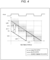
- Fig. 4 illustrates a method of combining the coarse TDC 132 and the fine TDC 133.
- lines L21 to L23 correspond to lines L11 to L13 in B of Fig. 3 .
- the nearest neighbor correction unit 152 and the adder 154 compare the output of the coarse TDC 132 with the output of the fine TDC 133, and select, among the numbers of integral multiples of 1/N, a value V n that makes the output of the fine TDC 133 closest to the range indicated by the output of the coarse TDC 132 when the value is added thereto, and add the selected value to the output of the fine TDC 133.
- the range corresponding to the region shaded with dots indicates the phase relationship of the coarse TDC 132 is in the range of 0.75 to 1 unless rounded down due to the resolution, and +0.5, which is a value that makes the output of the fine TDC 133 closest to the center of the range when the value is added thereto, is selected as V n and added (A11 in Fig. 4 ).
- Fig. 5 is a diagram illustrating an example of an operation table of the output generation unit 135.
- the operation table stores V n corresponding to the outputs of the coarse TDC 132 and the fine TDC 133.
- the nearest neighbor correction unit 152 and the adder 154 perform case classification according to the output of the coarse TDC 132 and the output of the fine TDC 133, and select the output V n from the operation table of Fig. 5 .
- a desired combined TDC output can be obtained.
- Fig. 6 is a timing chart illustrating an operation example of the coarse TDC 132 and the fine TDC 133 in a case where a clock skew exists. That is, the timing chart of Fig. 6 corresponds to the timing chart of Fig. 3 , and illustrates an example of a case where a clock skew that does not exist in a case of Fig. 3 exists.
- a of Fig. 6 illustrates a situation in which REFCLK_fine, which is an input of the fine TDC 133, is delayed by 0.2 with respect to REFCLK, which is an input of the coarse TDC 132.
- 1/N is equal to the output conversion measurement range of the fine TDC 133, and Rc represents the resolution of the coarse TDC 132 converted for the output.
- Fig. 7 is a diagram for describing addition of a skew estimation value.
- lines L41 and L42 correspond to the lines L31 and L32 in B of Fig. 6 , and indicate the output of the coarse TDC 132 and the output of the fine TDC 133.
- a line L43 indicates an output obtained by adding the skew estimation value to the output of the fine TDC 133.
- the adder 153 adds the skew estimation value to the output of the fine TDC 133.
- 0.2 is added to the output of the fine TDC 133 as the skew estimation value (A21 in the figure). Then, as illustrated in Fig.
- the nearest neighbor correction unit 152 and the adder 154 compare the output of the coarse TDC 132 with the output of the fine TDC 133, and select, among the numbers of integral multiples of 1/N, a value V n that makes the output of the fine TDC 133 closest to the range indicated by the output of the coarse TDC 132 when the value is added thereto, and add the selected value to the output of the fine TDC 133.
- FIG. 8 lines L51 and L52 correspond to the lines L41 and L43 in Fig. 7 , and indicate the output of the coarse TDC 132 and the output obtained by adding the skew estimation value to the output of the fine TDC 133. Furthermore, a line L53 indicates the combined TDC output. In Fig. 8 , V n of ⁇ 0.5 is selected and added to the output obtained by adding the skew estimation value to the fine TDC 133 so that the result of addition of the value becomes closest to the range of the value indicated by the output of the coarse TDC 132 (A31 and A32 in the figure).
- Fig. 9 is a diagram illustrating an example of an operation table of the output generation unit 135.
- the operation table stores V n corresponding to the outputs of the coarse TDC 132 and the fine TDC 133.
- the operation table of Fig. 9 is different from the operation table of Fig. 5 in that the range of possible values is enlarged because the output of the fine TDC 133 after the addition of the skew estimation value is used.
- the nearest neighbor correction unit 152 and the adder 154 perform case classification according to the output of the coarse TDC 132 and the output of the fine TDC 133 after the addition of the skew estimation value, and select the output V n from the operation table of Fig. 9 .
- the operation table of Fig. 9 is different from the operation table of Fig. 5 in that the possible range of the value is enlarged, but the operation is performed in the same manner as in Figs. 4 and 5 in that a value that makes the output closest to the range indicated by the output of the coarse TDC 132 when the value is added thereto is selected and added.
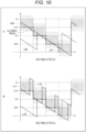
- Fig. 10 is a diagram for describing the influence of the skew estimation value error. In this condition, the above constraint is within ⁇ 0.125.
- lines L61 and L71 indicate the output of the coarse TDC 132
- lines L62 and L72 indicate the output of the fine TDC 133 after addition of the skew estimation value
- lines L63 and L73 indicate the combined TDC output.
- a of Fig. 10 illustrates a case where the error of the skew estimation value is -0.1 and within the constraint.
- the combined TDC output is generated to be a continuous value even at rising timings of REFCLK on the horizontal axis, as indicated by the line L63 in A of Fig. 10 .
- B of Fig. 10 illustrates a case where the error of the skew estimation value is -0.2 exceeding the above constraint.
- the combined TDC output becomes discontinuous at the rise timings of REFCLK.
- the above constraint corresponds to a value indicated by an arrow of "allowable error" in A of Fig. 10 , and this value matches the margin of the phase relationship having the smallest margin with respect to the nearest neighbor correction. That is, there is no problem even if there is an error in the skew estimation value up to the range ( ⁇ 0.125) corresponding to the region shaded by the dots in the figure. On the other hand, if there is an error in the skew estimation value exceeding the range ( ⁇ 0.125), the phase becomes discontinuous, which causes a problem.
- the results of the combined TDC output in the cases where there are different skew estimation errors obtained by the system simulation of the ADPLL circuit 10 are illustrated in Figs. 11 and 12 .
- the output frequency of the ADPLL circuit 10 is set such that the rise timing of REFCLK with respect to VCLK gradually shifts every cycle, and a skew of 0.2, which is normalized by VCLK_DIV, is provided between the coarse TDC 132 and the fine TDC 133.
- Fig. 11 illustrates a simulation result in a case where the skew estimation value is shifted by -0.1.
- this simulation result as indicated by a line L81 in Fig. 11 , a continuous combined TDC output as assumed in A in Fig. 10 described above is obtained.
- Fig. 12 illustrates a simulation result in a case where the skew estimation value is shifted by -0.2 (in a case where the skew estimation value exceeds the constraint of ⁇ 0.125 described above). In this simulation result, it is confirmed that a discontinuous output as assumed in B of Fig. 10 described above is obtained.
- the skew estimation value can be determined from a delay difference between the clock paths obtained by circuit simulation.
- the skew estimation value may be determined by sweeping the skew estimation value in actual measurement and determining a value that makes the combined TDC output continuous.
- Fig. 13 illustrates a system simulation result of the ADPLL circuit 10 when a skew of 250 psec exists between the coarse TDC 132 and the fine TDC 133 and the error of the skew estimation value is sufficiently small.
- the PHF sel signal is changed from “0" to "1" at 15000 cycles.
- the fine TDC 133 is enabled by the fine TDC EN signal to shift the operation to the normal operation (S16 and S17). Thereafter, the PHF sel signal is switched from "0" to "1" (S18). As a result, the outputs of the coarse TDC 132 and the fine TDC 133 are combined to output fine phase difference information.
- the fine TDC 133 is enabled after the phase lock of the ADPLL circuit 10.
- fine TDC 133 is not enabled ("No" in S15)
- coarse phase difference information is output using only the coarse TDC 132.
- the fine TDC 133 is enabled after the phase lead-in is started (S33) ("Yes" in S34).
- the fine TDC 133 is enabled and the operation shifts to the normal operation (S35 and S36).
- the PHF sel signal is switched to "1" (S37).
- the phase lead-in is continued (S38), and the phase is locked (S39). That is, in the operation of the ADPLL circuit 10 illustrated in Fig. 15 , the fine TDC 133 is enabled during the phase lead-in (before the phase lock).
- the fine TDC 133 is enabled and the operation shifts to the normal operation (S54 and S55). Thereafter, the PHF sel signal is switched to "1" (S56). Then, in the ADPLL circuit 10, the phase lead-in is started (S57), and the phase is locked (S58). That is, in the operation of the ADPLL circuit 10 illustrated in Fig. 16 , the fine TDC 133 is enabled before the phase lead-in.
- the coarse TDC 132 and the fine TDC 133 which are two TDCs having different resolutions are arranged in parallel, and the fine TDC 133 can be disabled. Therefore, it is possible to provide an operation mode switching function of performing a low power consumption operation using only the coarse TDC 132 in a case where a bad jitter is allowed, and performing a high resolution operation by combining the coarse TDC 132 and the fine TDC 133 in a case where a low jitter is required.
- the sel edge signal is output by the coarse TDC 132, which is easily downsized, so that a design such as a skew design that matches the clock synchronization unit 108 is facilitated. Moreover, an additional buffer or the like is unnecessary, and power consumption can be reduced.
- the output generation unit 135 can combine the outputs of the two TDCs, the coarse TDC 132 and the fine TDC 133, to generate and output the phase difference information.
- the phase difference information is output on the basis of the PHF sel signal different from the fine TDC EN signal of the fine TDC 133, so that the influence of the unstable operation immediately after enabling the fine TDC 133 on the loop operation is avoided and seamless operation mode switching can be realized.
- VCLK toward the coarse TDC 132, the clock synchronization unit 108, and the accumulator 109 can be replaced with VCLK_DIV obtained by dividing VCLK by N using the N frequency divider 131.
- the power consumption of the coarse TDC 132, the clock synchronization unit 108, and the accumulator 109 is reduced by the slow clock operation due to the N frequency divider 131 while the resolution of the information of the coarse TDC 132 is constrained and the information of the fine TDC 133 is interpolated in the information of the coarse TDC 132, so that the phase difference information can be correctly obtained without missing any information.
- the output generation unit 135 can add a skew estimation value corresponding to the skew between the coarse TDC 132 and the fine TDC 133 to the output of the fine TDC 133. Therefore, it is possible to correct the mismatch due to the clock skew between the coarse TDC 132 and the fine TDC 133 using the skew estimation value, and output correct phase difference information.
- a required jitter differs depending on use.
- the resolution required for the TDC also differs depending on the required jitter.
- a delay line TDC as disclosed in Patent Document 1 described above can be used.
- a vernier TDC as disclosed in Patent Document 3 described above can be used.
- Fig. 17 illustrates a configuration of a general ADPLL circuit 20.
- a control unit 200 to an accumulator 209 are illustrated corresponding to the control unit 100 to the accumulator 109 in Fig. 1 , but the configuration of the TDC207 in Fig. 17 is different from the configuration of the TDC 107 in Fig. 1 .
- the TDC207 can be configured using a delay line TDC or a vernier TDC, but is different from a configuration like the configuration of the TDC 107 in Fig. 1 , in which two TDCs, the coarse TDC 132 and the fine TDC 133 are arranged in parallel, and the fine TDC 133 can be disabled. Therefore, the enable signal (fine TDC EN signal) and the output selection signal (PHF sel signal) are not input to the TDC207.
- the configuration using the TDC207 having a high resolution is used so as to satisfy the requirement for low jitter applications.
- this configuration is used for applications in which low jitter is not required, power consumption increases as compared with the optimal design.
- the ratio of the power consumption of the TDC207 in the ADPLL circuit 20 is large and has a large influence. Therefore, it is desirable to reduce the resolution of the TDC in accordance with the jitter requirement, and the power consumption accordingly.
- the frequency divider 206 is not necessarily provided.
- Fig. 18 illustrates a configuration of an ADPLL circuit 30 that provides a resolution switching function with the current technology.
- a control unit 300 to an accumulator 309 are illustrated corresponding to the control unit 100 to the accumulator 109 in Fig. 1 , but the ADPLL circuit 30 has a configuration in which a TDC307-1 and a TDC307-2 in Fig. 18 are provided instead of the TDC 107 in Fig. 1 .
- the ADPLL circuit 30 of Fig. 18 has a configuration, in which the two independent TDCs, the TDC307-1 and the TDC307-2, are selectively used, and thus a selector 310 that selects one of the clock synchronization selection signals (sel edge signals) output from the two TDCs and outputs the selected signal to the clock synchronization unit 308 and a selector 311 that selects one of the outputs of the two TDCs are provided.
- a selector 310 that selects one of the clock synchronization selection signals (sel edge signals) output from the two TDCs and outputs the selected signal to the clock synchronization unit 308 and a selector 311 that selects one of the outputs of the two TDCs are provided.
- the coarse TDC 132 ( Fig. 2 ) having a coarse resolution and a small size can be arranged in the vicinity of the clock synchronization unit 108, and the clock skew can be minimized as described above.
- the frequency divider 306 is not necessarily provided.
- the configuration of the TDC 107 of Fig. 2 in which the N frequency divider 131 is provided has been described, but the N frequency divider 131 is not necessarily provided. Furthermore, the N frequency divider 131 may be configured to generate a multiphase clock.
- the fine TDC 133 that can be disabled may be enabled and then switched to disable by switching the input of the fine TDC EN signal.
- the fine TDC 133 is disabled as an initial setting, and then the fine TDC 133 can be enabled, but the enabled fine TDC 133 can be further disabled thereafter.
- the present disclosure can have the following configurations.
Landscapes
- Stabilization Of Oscillater, Synchronisation, Frequency Synthesizers (AREA)
Abstract
Description
- The present disclosure relates to an all digital phase-locked loop circuit, and in particular to an all digital phase-locked loop circuit that can be more easily designed.
- There is an all digital PLL (ADPLL) circuit in which all components of a phase locked loop (PLL) circuit are digitized. The ADPLL circuit has a configuration in which a time to digital converter (TDC) is used to extract phase difference information of an output of a digitally controlled oscillator (DCO) that controls a frequency by digital control.
- For example, as a configuration using a TDC in the ADPLL circuit, there are configurations disclosed in
Patent Documents -
- Patent Document 1:
Japanese Patent Application Laid-Open No. 2002-76886 - Patent Document 2:
Japanese Patent Application Laid-Open No. 2015-154444 - Patent Document 3:
Japanese Patent Application Laid-Open No. 2009-246484 - In a case where the configuration using the TDC in the ADPLL circuit is adopted, it is required to design the ADPLL circuit more easily.
- The present disclosure has been made in view of such a situation, and an object of the present disclosure is to enable design more easily.
- An all digital phase-locked loop circuit according to one aspect of the present disclosure includes: a first time-to-digital converter that performs phase difference detection at a first resolution; and a second time-to-digital converter that performs phase difference detection at a second resolution finer than the first resolution and that is arranged in parallel with the first time-to-digital converter, in which the second time-to-digital converter is configured to allow being disabled, and the first time-to-digital converter outputs a clock synchronization selection signal used for synchronizing a reference clock signal to a clock synchronization unit that generates a clock signal of a digital part.
- In an all digital phase-locked loop circuit according to one aspect of the present disclosure, a first time-to-digital converter that performs phase difference detection at a first resolution and a second time-to-digital converter that performs phase difference detection at a second resolution finer than the first resolution are arranged in parallel, in which the second time-to-digital converter is configured to allow being disabled, and the first time-to-digital converter outputs a clock synchronization selection signal used for synchronizing a reference clock signal to a clock synchronization unit that generates a clock signal of a digital part.
- Note that the all digital phase-locked loop circuit according to one aspect of the present disclosure may be an independent device or an internal block configuring one device.
-
-
Fig. 1 is a block diagram illustrating a configuration example of an embodiment of an ADPLL circuit to which the present disclosure is applied. -
Fig. 2 is a block diagram illustrating an example configuration of a TDC. -
Fig. 3 is a timing chart illustrating an operation example of a coarse TDC and a fine TDC. -
Fig. 4 is a timing chart illustrating an operation example of an output generation unit. -
Fig. 5 is a diagram illustrating an example of an operation table of the output generation unit. -
Fig. 6 is a timing chart illustrating an operation example of the coarse TDC and the fine TDC in a case where a clock skew exists. -
Fig. 7 is a diagram for describing an addition example of a skew estimation value. -
Fig. 8 is a timing chart illustrating an operation example of the output generation unit at the time of adding the skew estimation value. -
Fig. 9 is a diagram illustrating an example of an operation table of the output generation unit at the time of adding the skew estimation value. -
Fig. 10 is a diagram for describing the influence of a skew estimation value error. -
Fig. 11 is a diagram illustrating a first example of a combined TDC output according to a system simulation result of the ADPLL circuit in a case where a skew estimation value error exists. -
Fig. 12 is a diagram illustrating a second example of a combined TDC output according to a system simulation result of the ADPLL circuit in a case where a skew estimation value error exists. -
Fig. 13 is a diagram illustrating an example of a system simulation result of the ADPLL circuit. -
Fig. 14 is a flowchart for describing a first example of the operation of the ADPLL circuit. -
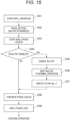
Fig. 15 is a flowchart illustrating a second example of the operation of the ADPLL circuit. -
Fig. 16 is a flowchart for describing a third example of the operation of the ADPLL circuit. -
Fig. 17 is a block diagram illustrating a configuration example of a general ADPLL circuit. -
Fig. 18 is a block diagram illustrating a configuration example of an ADPLL circuit that provides a resolution switching function with the current technology. -
Fig. 1 is a block diagram illustrating a configuration example of an embodiment of an ADPLL circuit to which the present disclosure is applied. - An
ADPLL circuit 10 is an all digital phase-locked loop circuit that generates an output from a DCO that controls a frequency by digital control, from a digital frequency control input (frequency command word (FCW)) and a reference frequency input (reference clock signal: REFCLK) from the outside, adjusts the DCO on the basis of a difference from the FCW obtained from the output signal, and performs an operation of adjusting the output to a control value by the FCW based on the reference frequency input. - In
Fig. 1 , theADPLL circuit 10 includes acontrol unit 100, anREF accumulator 101, anadder 102, aloop filter 103, an OTWIF 104, aDCO 105, afrequency divider 106, aTDC 107, aclock synchronization unit 108, and anaccumulator 109. Thecontrol unit 100 controls the operation of each unit of theADPLL circuit 10. - The
DCO 105 is a digitally controlled oscillator that outputs a signal having an oscillation frequency indicated by an oscillator control word (oscillator tuning word (OTW)) input from the OTW IF 104. An output signal output from theDCO 105 is an output (clock signal: CLK) of theADPLL circuit 10. The frequency divider 106 frequency-divides an output signal from theDCO 105 at a predetermined frequency division ratio, and outputs the signal to theTDC 107 as a frequency-divided output signal (VCLK). Note that thefrequency divider 106 is provided as necessary, and in a case where thefrequency divider 106 is not provided, the output signal from theDCO 105 is directly input to theTDC 107 as VCLK. In the following description, a case where thefrequency divider 106 is provided as illustrated inFig. 1 and VCLK from thefrequency divider 106 is input to theTDC 107 will be described. - The
TDC 107 is a time-to-digital converter that detects phase difference information of an output signal of theDCO 105 from REFCLK input as a reference clock signal and VCLK input from thefrequency divider 106. TheTDC 107 outputs the phase difference information to theadder 102. Furthermore, theTDC 107 outputs a VCLK_DIV obtained by dividing VCLK at a predetermined frequency division ratio to theclock synchronization unit 108 and theaccumulator 109. - The
TDC 107 outputs a clock synchronization selection signal (hereinafter, also referred to as a sel edge signal) used for synchronizing REFCLK with VCLK_DIV to theclock synchronization unit 108. Furthermore, an enable signal (hereinafter, also referred to as a fine TDC EN signal) and an output selection signal (hereinafter, also referred to as a PHF sel signal) are input to theTDC 107 under the control of thecontrol unit 100. Details of the configuration of theTDC 107 will be described later with reference toFig. 2 . - The
clock synchronization unit 108 generates RTREFCLK by synchronizing REFCLK input as a reference clock signal using the sel edge signal and VCLK_DIV input from theTDC 107, and outputs RTREFCLK to each unit. The RTREFCLK is a clock signal of the digital part of theADPLL circuit 10. Theaccumulator 109 functions as a counter that accumulates a predetermined value (for example, 1) in synchronization with VCLK_DIV input from theTDC 107, and outputs the accumulated value to theadder 102. - The
REF accumulator 101 inputs phase control information obtained from FCW input thereto to theadder 102. Theadder 102 adds the output (accumulated value as an integer part) from theaccumulator 109 and the output (phase difference information as a decimal part) from theTDC 107 to obtain phase information. Furthermore, theadder 102 subtracts the phase information obtained by the addition from the phase control information input from theREF accumulator 101 to generate phase error information, and outputs the phase error information to theloop filter 103. - The
loop filter 103 performs filter processing on the phase error information input from theadder 102, generates a control value for theDCO 105, and outputs the control value to the OTW IF 104. The OTW IF 104 generates OTW on the basis of the control value input from theloop filter 103 and outputs OTW to theDCO 105. The oscillation frequency of theDCO 105 is controlled by repeating the above-described operation. -
Fig. 2 is a block diagram illustrating an example configuration of theTDC 107 illustrated inFig. 1 . - In
Fig. 2 , the TDC 107 includes anN frequency divider 131, acoarse TDC 132, afine TDC 133, and anoutput generation unit 135. Thefine TDC 133 includes a fine TDCmain circuit 133A and a 1/N multiplier 134. - In the
TDC 107, acoarse TDC 132 and afine TDC 133 are provided in parallel. Thecoarse TDC 132 performs phase difference detection at a first resolution. Thefine TDC 133 performs phase difference detection at a second resolution finer than the first resolution. Thefine TDC 133 can be disabled by the fine TDC EN signal. Thecoarse TDC 132 outputs the sel edge signal to theclock synchronization unit 108. - In a case where a bad jitter is allowed in the
ADPLL circuit 10, thefine TDC 133 is disabled and only thecoarse TDC 132 can be used to achieve a low power consumption operation. On the other hand, in a case where a low jitter is required in theADPLL circuit 10, thefine TDC 133 is enabled and thecoarse TDC 132 and thefine TDC 133 can be combined to achieve a high resolution operation. - In general, it is necessary to minimize a clock skew (time difference of clocks) between the
clock synchronization unit 108 and the TDC 107 (coarse TDC 132). This is because the sel edge signal generated on the basis of the phase difference information (phase difference information between REFCLK and VCLK_DIV) measured by the TDC 107 (coarse TDC 132) is transmitted to theclock synchronization unit 108, and in response, theclock synchronization unit 108 selects a VCLK_DIV edge to synchronize REFCLK. The sel edge signal is a signal indicating which of the rise and fall of VCLK_DIV is farther from REFCLK edge. - At the time of synchronization, if the timings of the rise of REFCLK and the synchronization edge of VCLK_DIV are too close to each other, metastability occurs, and a problem occurs in subsequent signal processing. Therefore, a sel edge signal is used to avoid the problem. As a premise, in the
clock synchronization unit 108, the phase relationship between REFCLK and VCLK_DIV and the phase relationship with thecoarse TDC 132 need to be the same, and thus minimization of the clock skew is required. In theADPLL circuit 10, thecoarse TDC 132 having a coarse resolution and a small size can be arranged (physically) close to theclock synchronization unit 108 in theTDC 107, and the clock skew can be minimized. - As described above, the
TDC 107 can realize the operation mode switching function of performing the low power consumption operation using only thecoarse TDC 132 in a case where a bad jitter is allowed, and performing the high resolution operation with thefine TDC 133 when a low jitter is required. Furthermore, in theTDC 107, the sel edge signal is output from thecoarse TDC 132, which is easily downsized, so that a clock skew design that matches theclock synchronization unit 108 is facilitated. - In the
TDC 107, theoutput generation unit 135 outputs phase difference information (PHF) on the basis of the output of the coarse TDC 132 (PHF1), the output of the fine TDC 133 (PHF2), and the PHF sel signal. Here, when thefine TDC 133 is disabled, the phase difference information (PHF) is output on the basis of the output (PHF1) of thecoarse TDC 132. On the other hand, when thefine TDC 133 is enabled, the phase difference information (PHF) is output on the basis of the output (PHF1) of thecoarse TDC 132, the output (PHF2) of thefine TDC 133, and the PHF sel. - Since the
coarse TDC 132 and thefine TDC 133 have different outputs, theoutput generation unit 135 outputs a combination of these TDC outputs. In a case where thefine TDC 133 is disabled, the output of thecoarse TDC 132 is output as it is (or may be delayed). In a case where thefine TDC 133 is enabled, the output of thecoarse TDC 132 can be output as it is or a value generated by combining the outputs of thecoarse TDC 132 and thefine TDC 133 can be output on the basis of the PHF sel signal. - The
fine TDC 133 typically performs averaging processing to obtain the period of VCLK therein, and may output an instable value immediately after being enabled. Therefore, by controlling theoutput generation unit 135 using the PHF sel signal different from the fine TDC EN signal of thefine TDC 133, propagation of the instable value to subsequent stages, and then malfunction of theADPLL circuit 10 can be prevented. Furthermore, thefine TDC 133 is enabled in advance, and the PHF sel signal is switched at a necessary timing after stabilization, whereby seamless operation mode switching can be realized. - As described above, the
output generation unit 135 can generate phase difference information by combining the output of thecoarse TDC 132 and the output of thefine TDC 133. Furthermore, theoutput generation unit 135 performs output on the basis of the PHF sel signal different from the fine TDC EN signal of thefine TDC 133, so that it is possible to avoid the influence of the unstable operation immediately after enabling thefine TDC 133 on the loop operation and realize seamless operation mode switching. - The
N frequency divider 131 is provided for a VCLK input common to thecoarse TDC 132, theclock synchronization unit 108, and theaccumulator 109. Here, N is an integer. In this case, the resolution of thecoarse TDC 132 converted for the output needs to be finer than 1/N. That is, since the output conversion measurement range (hereinafter, also referred to as a measurement range) of thefine TDC 133 is 1/N and the measurement range converted for input of thefine TDC 133 matches the VCLK period, the resolution of thecoarse TDC 132 is finer than VCLK period. - Here, in the
TDC 107 of theADPLL circuit 10, as a general definition, the input conversion measurement range is assumed to match the period of the high-speed clock input (VCLK). Furthermore, it is assumed that the output of theTDC 107 is obtained by normalizing the time difference between REFCLK and VCLK by the period of the high-speed clock input (VCLK). That is, the output of theTDC 107 is in the range of 0 to 1. - In a case where the
N frequency divider 131 is provided, the denominator of normalization becomes N times, the input range increases by N times, and then the output value becomes 1/N times those in a case where theN frequency divider 131 is not provided, although the time difference is the same. In thefine TDC 133, the 1/N multiplier 134 is arranged at the subsequent stage of the fine TDCmain circuit 133A that performs phase difference detection in order to match the input time difference with the relationship between the output values between thecoarse TDC 132 and thefine TDC 133 in consideration of the change in the output of thecoarse TDC 132 by theN frequency divider 131. - As described above, the slow clock operation due to the
N frequency divider 131 can reduce the power consumption of thecoarse TDC 132, theclock synchronization unit 108, and theaccumulator 109. Moreover, by restricting the resolution of thecoarse TDC 132, the information of thecoarse TDC 132 can be interpolated with the information of thefine TDC 133, and the phase difference information can be correctly obtained without missing any information. - The restriction of the resolution of the
coarse TDC 132 described above means that 1 LSB of thecoarse TDC 132 <= the output conversion measurement range of the fine TDC 133 (=1/N) is required to fill the interval in the coarse 1 LSB of thecoarse TDC 132 with the fine resolution of thefine TDC 133. In a case where this is not satisfied, the interval in the 1 LSB of thecoarse TDC 132 cannot be filled without any gap. - The
output generation unit 135 includes aselector 151, a nearestneighbor correction unit 152, anadder 153, and anadder 154. - The nearest
neighbor correction unit 152 and theadder 154 add a value corresponding to an integral multiple of 1/N (= the output conversion measurement range of the fine TDC 133) (N is a frequency division ratio of the N frequency divider 131) to the output of thefine TDC 133 to correct the addition result to a value most matching the output of thecoarse TDC 132. That is, by performing such correction, the output of thecoarse TDC 132 and the output of thefine TDC 133 are specifically combined. Details of operations of the nearestneighbor correction unit 152 and theadder 154 in theoutput generation unit 135 will be described later with reference toFigs. 3 to 5 . - The
adder 153 adds a value (hereinafter, also referred to as a skew estimation value) corresponding to the skew between thecoarse TDC 132 and thefine TDC 133 to the output of thefine TDC 133. As a result, it is possible to correct the mismatch of the result due to the skew existing between thecoarse TDC 132 and thefine TDC 133 and output correct phase difference information. Details of the operation of theoutput generation unit 135 at the time of adding the skew estimation value will be described later with reference toFigs. 6 to 12 . - The
selector 151 selects, on the basis of the PHF sel signal, the output of thecoarse TDC 132 or the output generated on the basis of the output of thecoarse TDC 132 and the output of thefine TDC 133, and outputs the selected output as phase difference information (PHF). Thecontrol unit 100 independently controls the fine TDC EN signal input to thefine TDC 133 and the PHF sel signal input to theselector 151. - The
TDC 107 is configured as described above. With this configuration, for example, the following effects can be obtained. That is, since thecoarse TDC 132 and thefine TDC 133 that can be disabled are provided in parallel, it is possible to provide the operation mode switching function of performing the low power consumption operation using only thecoarse TDC 132 in a case where a bad jitter is allowed, and performing the high resolution operation in which thecoarse TDC 132 and thefine TDC 133 are combined when a low jitter is required. Furthermore, the sel edge signal is output from thecoarse TDC 132, which is easily downsized, so that a skew design that matches theclock synchronization unit 108 can be easily realized. - Furthermore, the power consumption of the
coarse TDC 132, theclock synchronization unit 108, and theaccumulator 109 is reduced by the slow clock operation due to theN frequency divider 131 while the information of thefine TDC 133 is interpolated in the information of thecoarse TDC 132, so that the phase difference information can be correctly obtained without missing any information. Moreover, it is possible to correct the mismatch due to the skew between thecoarse TDC 132 and thefine TDC 133 using the skew estimation value and output correct phase difference information. - Next, the operation content of the
output generation unit 135 will be described with reference toFigs. 3 to 5 . Here, a 2 frequency divider is used as theN frequency divider 131, and the resolution of thecoarse TDC 132 converted for the output is set to 0.25. In addition, values stated herein are values normalized by one period of VCLK_DIV. -
Fig. 3 is a timing chart illustrating an operation example of thecoarse TDC 132 and thefine TDC 133 ofFig. 2 . A ofFig. 3 illustrates a relationship between the TDC input timing chart and the measurement edge. In A ofFig. 3 , VCLK_DIV and REFCLK are signals input to thecoarse TDC 132, and VCLK_fine and REFCLK_fine are signals input to thefine TDC 133. - The
coarse TDC 132 measures the time from the rise of REFCLK to the rise of VCLK_DIV. Thefine TDC 133 measures the time from the rise of REFCLK_fine (here, the same signal as REFCLK) to the rise of VCLK_fine. - As illustrated in A of
Fig. 3 , REFCLK (REFCLK_fine) rises at a position of 0.9 for thecoarse TDC 132 and at a position of 0.4 for thefine TDC 133. Each of thecoarse TDC 132 and thefine TDC 133 measures time corresponding to the rise timing. However, since the resolution is finite, the output values are values obtained by rounding down by intervals determined by the resolutions. - B of
Fig. 3 illustrates the relationship between the rise timings of REFCLK and the TDC output. In B ofFig. 3 , the horizontal axis represents the rising timing of REFCLK, and the vertical axis represents the output value of each TDC. - As indicated by a line L11, the
coarse TDC 132 is output in a coarse stepwise manner corresponding to the resolution 0.25. As indicated by the line L12, thefine TDC 133 has a fine resolution, and thus is output substantially linearly. Thefine TDC 133 has an output conversion measurement range of 1/N, and when the output value exceeds 1/N, it is compared with the next edge of VCLK_fine, so that an output as folded back at 0.5 is obtained. - As a desired method of combining the
coarse TDC 132 and thefine TDC 133, a straight line indicated by a line L13 having a wide measurement range of thecoarse TDC 132 and afine resolution 133 of the fine TDC is desirable. -
Fig. 4 illustrates a method of combining thecoarse TDC 132 and thefine TDC 133. InFig. 4 , lines L21 to L23 correspond to lines L11 to L13 in B ofFig. 3 . In theoutput generation unit 135, the nearestneighbor correction unit 152 and theadder 154 compare the output of thecoarse TDC 132 with the output of thefine TDC 133, and select, among the numbers of integral multiples of 1/N, a value Vn that makes the output of thefine TDC 133 closest to the range indicated by the output of thecoarse TDC 132 when the value is added thereto, and add the selected value to the output of thefine TDC 133. - Specifically, in
Fig. 4 , for example, when thecoarse TDC 132 outputs 0.75, the range corresponding to the region shaded with dots indicates the phase relationship of thecoarse TDC 132 is in the range of 0.75 to 1 unless rounded down due to the resolution, and +0.5, which is a value that makes the output of thefine TDC 133 closest to the center of the range when the value is added thereto, is selected as Vn and added (A11 inFig. 4 ). -
Fig. 5 is a diagram illustrating an example of an operation table of theoutput generation unit 135. InFig. 5 , the operation table stores Vn corresponding to the outputs of thecoarse TDC 132 and thefine TDC 133. As a result, the nearestneighbor correction unit 152 and theadder 154 perform case classification according to the output of thecoarse TDC 132 and the output of thefine TDC 133, and select the output Vn from the operation table ofFig. 5 . With this combination method, a desired combined TDC output can be obtained. - Next, the operation content of the
output generation unit 135 at the time of adding skew estimation value will be described with reference toFigs. 6 to 12 . In a case where different delays (clock skew) exist on the clock paths of thecoarse TDC 132 and thefine TDC 133, the results of thecoarse TDC 132 and thefine TDC 133 have a mismatch relationship. -
Fig. 6 is a timing chart illustrating an operation example of thecoarse TDC 132 and thefine TDC 133 in a case where a clock skew exists. That is, the timing chart ofFig. 6 corresponds to the timing chart ofFig. 3 , and illustrates an example of a case where a clock skew that does not exist in a case ofFig. 3 exists. - In a case where a clock skew exists, the results of the
coarse TDC 132 and thefine TDC 133 have a mismatch relationship, and this relationship is illustrated in A ofFig. 6 . A ofFig. 6 illustrates a situation in which REFCLK_fine, which is an input of thefine TDC 133, is delayed by 0.2 with respect to REFCLK, which is an input of thecoarse TDC 132. - In this case, as illustrated in B of
Fig. 6 , the output of thefine TDC 133 is shifted leftward by 0.2 as a whole due to the influence of the skew. That is, in B ofFig. 6 , lines L31 to L33 correspond to the lines L11 to L13 in B ofFig. 3 , but only the line L32 indicating the output of thefine TDC 133 is shifted leftward. At this time, by simulation, evaluation, or the like, the skew is estimated with an error within a value obtained from the following Formula (1), and the configuration of theoutput generation unit 135 inFig. 2 enables correction for the influence of the skew using the skew estimation value, so that a correct output can be obtained.
- However, in Formula (1), 1/N is equal to the output conversion measurement range of the
fine TDC 133, and Rc represents the resolution of thecoarse TDC 132 converted for the output. Under the conditions in the figure, the allowable error is ±(0.5 - 0.25) ÷ 2 = ±0.125. -
Fig. 7 is a diagram for describing addition of a skew estimation value. InFig. 7 , lines L41 and L42 correspond to the lines L31 and L32 in B ofFig. 6 , and indicate the output of thecoarse TDC 132 and the output of thefine TDC 133. Furthermore, a line L43 indicates an output obtained by adding the skew estimation value to the output of thefine TDC 133. - As illustrated in
Fig. 7 , first, theadder 153 adds the skew estimation value to the output of thefine TDC 133. InFig. 7 , as illustrated by the relationship between the line L42 and the line L43, 0.2 is added to the output of thefine TDC 133 as the skew estimation value (A21 in the figure). Then, as illustrated inFig. 8 , the nearestneighbor correction unit 152 and theadder 154 compare the output of thecoarse TDC 132 with the output of thefine TDC 133, and select, among the numbers of integral multiples of 1/N, a value Vn that makes the output of thefine TDC 133 closest to the range indicated by the output of thecoarse TDC 132 when the value is added thereto, and add the selected value to the output of thefine TDC 133. - This procedure is similar to that of
Fig. 4 described above. With this procedure, a desired combined TDC output can be obtained. InFig. 8 , lines L51 and L52 correspond to the lines L41 and L43 inFig. 7 , and indicate the output of thecoarse TDC 132 and the output obtained by adding the skew estimation value to the output of thefine TDC 133. Furthermore, a line L53 indicates the combined TDC output. InFig. 8 , Vn of ±0.5 is selected and added to the output obtained by adding the skew estimation value to thefine TDC 133 so that the result of addition of the value becomes closest to the range of the value indicated by the output of the coarse TDC 132 (A31 and A32 in the figure). -
Fig. 9 is a diagram illustrating an example of an operation table of theoutput generation unit 135. InFig. 9 , the operation table stores Vn corresponding to the outputs of thecoarse TDC 132 and thefine TDC 133. The operation table ofFig. 9 is different from the operation table ofFig. 5 in that the range of possible values is enlarged because the output of thefine TDC 133 after the addition of the skew estimation value is used. - As a result, the nearest
neighbor correction unit 152 and theadder 154 perform case classification according to the output of thecoarse TDC 132 and the output of thefine TDC 133 after the addition of the skew estimation value, and select the output Vn from the operation table ofFig. 9 . The operation table ofFig. 9 is different from the operation table ofFig. 5 in that the possible range of the value is enlarged, but the operation is performed in the same manner as inFigs. 4 and5 in that a value that makes the output closest to the range indicated by the output of thecoarse TDC 132 when the value is added thereto is selected and added. - Here, a constraint within a value obtained from the above Formula (1) will be described with reference to
Fig. 10. Fig. 10 is a diagram for describing the influence of the skew estimation value error. In this condition, the above constraint is within ±0.125. In A and B ofFig. 10 , lines L61 and L71 indicate the output of thecoarse TDC 132, lines L62 and L72 indicate the output of thefine TDC 133 after addition of the skew estimation value, and lines L63 and L73 indicate the combined TDC output. - A of
Fig. 10 illustrates a case where the error of the skew estimation value is -0.1 and within the constraint. In a case where the error of the skew estimation value does not exceed the above constraint, the combined TDC output is generated to be a continuous value even at rising timings of REFCLK on the horizontal axis, as indicated by the line L63 in A ofFig. 10 . - On the other hand, B of
Fig. 10 illustrates a case where the error of the skew estimation value is -0.2 exceeding the above constraint. In this case, as indicated by the line L73 in B ofFig. 10 , the combined TDC output becomes discontinuous at the rise timings of REFCLK. - Note that the above constraint corresponds to a value indicated by an arrow of "allowable error" in A of
Fig. 10 , and this value matches the margin of the phase relationship having the smallest margin with respect to the nearest neighbor correction. That is, there is no problem even if there is an error in the skew estimation value up to the range (±0.125) corresponding to the region shaded by the dots in the figure. On the other hand, if there is an error in the skew estimation value exceeding the range (±0.125), the phase becomes discontinuous, which causes a problem. - Here, the results of the combined TDC output in the cases where there are different skew estimation errors obtained by the system simulation of the
ADPLL circuit 10 are illustrated inFigs. 11 and12 . In this simulation, the output frequency of theADPLL circuit 10 is set such that the rise timing of REFCLK with respect to VCLK gradually shifts every cycle, and a skew of 0.2, which is normalized by VCLK_DIV, is provided between thecoarse TDC 132 and thefine TDC 133. -
Fig. 11 illustrates a simulation result in a case where the skew estimation value is shifted by -0.1. In this simulation result, as indicated by a line L81 inFig. 11 , a continuous combined TDC output as assumed in A inFig. 10 described above is obtained. - On the other hand,
Fig. 12 illustrates a simulation result in a case where the skew estimation value is shifted by -0.2 (in a case where the skew estimation value exceeds the constraint of ±0.125 described above). In this simulation result, it is confirmed that a discontinuous output as assumed in B ofFig. 10 described above is obtained. - As a method of obtaining the skew estimation value, for example, the skew estimation value can be determined from a delay difference between the clock paths obtained by circuit simulation. Alternatively, the skew estimation value may be determined by sweeping the skew estimation value in actual measurement and determining a value that makes the combined TDC output continuous.
-
Fig. 13 illustrates a system simulation result of theADPLL circuit 10 when a skew of 250 psec exists between thecoarse TDC 132 and thefine TDC 133 and the error of the skew estimation value is sufficiently small. In this simulation, the PHF sel signal is changed from "0" to "1" at 15000 cycles. - That is, before 15000 cycles, coarse phase difference information is output using only the
coarse TDC 132, and after 15000 cycles, fine phase difference information is output using thecoarse TDC 132 and thefine TDC 133. As indicated by the change of a line L91 inFig. 13 , it is indicated that the resolution of the combined TDC is smoothly switched before and after the change. - Next, the operation of the
ADPLL circuit 10 will be described with reference to flowcharts ofFigs. 14 to 16 . First, a basic operation of theADPLL circuit 10 will be described with reference to the flowchart ofFig. 14 . - As illustrated in
Fig. 14 , when the operation of theADPLL circuit 10 is started (S11), thefine TDC 133 is disabled (S12) as the initial setting, and only thecoarse TDC 132 is used. Then, in theADPLL circuit 10, phase lead-in is started (S13), and the phase is locked (S14). - At this time, in a case where the
fine TDC 133 is enabled ("Yes" in S15), thefine TDC 133 is enabled by the fine TDC EN signal to shift the operation to the normal operation (S16 and S17). Thereafter, the PHF sel signal is switched from "0" to "1" (S18). As a result, the outputs of thecoarse TDC 132 and thefine TDC 133 are combined to output fine phase difference information. Here, thefine TDC 133 is enabled after the phase lock of theADPLL circuit 10. - Furthermore, in a case where the
fine TDC 133 is not enabled ("No" in S15), coarse phase difference information is output using only thecoarse TDC 132. - Next, a modification of the operation of the
ADPLL circuit 10 will be described with reference to the flowcharts ofFigs. 15 and16 . However, inFigs. 15 and16 , similarly toFig. 14 (S11 and S12), thefine TDC 133 is disabled as the initial setting at the start of the operation of the ADPLL circuit 10 (S31 and S32 inFig. 15 and S51 and S52 inFig. 16 ). - As illustrated in
Fig. 15 , in theADPLL circuit 10, in a case where thefine TDC 133 is enabled after the phase lead-in is started (S33) ("Yes" in S34), thefine TDC 133 is enabled and the operation shifts to the normal operation (S35 and S36). Thereafter, the PHF sel signal is switched to "1" (S37). Then, in theADPLL circuit 10, the phase lead-in is continued (S38), and the phase is locked (S39). That is, in the operation of theADPLL circuit 10 illustrated inFig. 15 , thefine TDC 133 is enabled during the phase lead-in (before the phase lock). - As illustrated in
Fig. 16 , in theADPLL circuit 10, in a case where thefine TDC 133 is enabled ("Yes" in S53), thefine TDC 133 is enabled and the operation shifts to the normal operation (S54 and S55). Thereafter, the PHF sel signal is switched to "1" (S56). Then, in theADPLL circuit 10, the phase lead-in is started (S57), and the phase is locked (S58). That is, in the operation of theADPLL circuit 10 illustrated inFig. 16 , thefine TDC 133 is enabled before the phase lead-in. - As described above, in the
ADPLL circuit 10 to which the present disclosure is applied, thecoarse TDC 132 and thefine TDC 133, which are two TDCs having different resolutions are arranged in parallel, and thefine TDC 133 can be disabled. Therefore, it is possible to provide an operation mode switching function of performing a low power consumption operation using only thecoarse TDC 132 in a case where a bad jitter is allowed, and performing a high resolution operation by combining thecoarse TDC 132 and thefine TDC 133 in a case where a low jitter is required. Furthermore, in theADPLL circuit 10, the sel edge signal is output by thecoarse TDC 132, which is easily downsized, so that a design such as a skew design that matches theclock synchronization unit 108 is facilitated. Moreover, an additional buffer or the like is unnecessary, and power consumption can be reduced. - Furthermore, in the
ADPLL circuit 10, theoutput generation unit 135 can combine the outputs of the two TDCs, thecoarse TDC 132 and thefine TDC 133, to generate and output the phase difference information. Here, the phase difference information is output on the basis of the PHF sel signal different from the fine TDC EN signal of thefine TDC 133, so that the influence of the unstable operation immediately after enabling thefine TDC 133 on the loop operation is avoided and seamless operation mode switching can be realized. - Furthermore, in the
ADPLL circuit 10, VCLK toward thecoarse TDC 132, theclock synchronization unit 108, and theaccumulator 109 can be replaced with VCLK_DIV obtained by dividing VCLK by N using theN frequency divider 131. In that case, the resolution of thecoarse TDC 132 is made finer than the VCLK period (= the output conversion measurement range of the fine TDC 133). As a result, the power consumption of thecoarse TDC 132, theclock synchronization unit 108, and theaccumulator 109 is reduced by the slow clock operation due to theN frequency divider 131 while the resolution of the information of thecoarse TDC 132 is constrained and the information of thefine TDC 133 is interpolated in the information of thecoarse TDC 132, so that the phase difference information can be correctly obtained without missing any information. - Furthermore, in the
ADPLL circuit 10, theoutput generation unit 135 can add a skew estimation value corresponding to the skew between thecoarse TDC 132 and thefine TDC 133 to the output of thefine TDC 133. Therefore, it is possible to correct the mismatch due to the clock skew between thecoarse TDC 132 and thefine TDC 133 using the skew estimation value, and output correct phase difference information. - Here, for the ADPLL circuit that is a clock source, a required jitter differs depending on use. The resolution required for the TDC also differs depending on the required jitter. In a case where the required resolution is not high, a delay line TDC as disclosed in
Patent Document 1 described above can be used. On the other hand, in a case where the required resolution is high, a vernier TDC as disclosed in Patent Document 3 described above can be used. -
Fig. 17 illustrates a configuration of ageneral ADPLL circuit 20. InFig. 17 , acontrol unit 200 to anaccumulator 209 are illustrated corresponding to thecontrol unit 100 to theaccumulator 109 inFig. 1 , but the configuration of the TDC207 inFig. 17 is different from the configuration of theTDC 107 inFig. 1 . That is, the TDC207 can be configured using a delay line TDC or a vernier TDC, but is different from a configuration like the configuration of theTDC 107 inFig. 1 , in which two TDCs, thecoarse TDC 132 and thefine TDC 133 are arranged in parallel, and thefine TDC 133 can be disabled. Therefore, the enable signal (fine TDC EN signal) and the output selection signal (PHF sel signal) are not input to the TDC207. - In a case where the one
ADPLL circuit 20 is used for various applications, the configuration using the TDC207 having a high resolution is used so as to satisfy the requirement for low jitter applications. On the other hand, in a case where this configuration is used for applications in which low jitter is not required, power consumption increases as compared with the optimal design. The ratio of the power consumption of the TDC207 in theADPLL circuit 20 is large and has a large influence. Therefore, it is desirable to reduce the resolution of the TDC in accordance with the jitter requirement, and the power consumption accordingly. Note that, also in theADPLL circuit 20 ofFig. 17 , thefrequency divider 206 is not necessarily provided. - It is possible to prepare two independent TDCs having different resolutions and use these two TDCs selectively even with the current technology.
Fig. 18 illustrates a configuration of anADPLL circuit 30 that provides a resolution switching function with the current technology. InFig. 18 , acontrol unit 300 to anaccumulator 309 are illustrated corresponding to thecontrol unit 100 to theaccumulator 109 inFig. 1 , but theADPLL circuit 30 has a configuration in which a TDC307-1 and a TDC307-2 inFig. 18 are provided instead of theTDC 107 inFig. 1 . - The
ADPLL circuit 30 ofFig. 18 has a configuration, in which the two independent TDCs, the TDC307-1 and the TDC307-2, are selectively used, and thus aselector 310 that selects one of the clock synchronization selection signals (sel edge signals) output from the two TDCs and outputs the selected signal to theclock synchronization unit 308 and aselector 311 that selects one of the outputs of the two TDCs are provided. In theADPLL circuit 30 ofFig. 18 , it is necessary to match a skew at three points including theclock synchronization unit 308 and two independent TDCs, the TDC307-1 and the TDC307-2, which makes it difficult to design. On the other hand, in theADPLL circuit 10 ofFig. 1 , the coarse TDC 132 (Fig. 2 ) having a coarse resolution and a small size can be arranged in the vicinity of theclock synchronization unit 108, and the clock skew can be minimized as described above. Note that, also in theADPLL circuit 30 ofFig. 18 , thefrequency divider 306 is not necessarily provided. - Furthermore, in a case where the resolution switching is realized by a 2-step TDC as disclosed in
Patent Document 2 stated above, other problems such as a complicated routing configuration of the 2-step TDC itself and occurrence of nonlinearity due to a time-amplifier occur. - In the above description, the configuration of the
TDC 107 ofFig. 2 , in which theN frequency divider 131 is provided has been described, but theN frequency divider 131 is not necessarily provided. Furthermore, theN frequency divider 131 may be configured to generate a multiphase clock. - In the
TDC 107, thefine TDC 133 that can be disabled may be enabled and then switched to disable by switching the input of the fine TDC EN signal. For example, in the ADPLL operation flow illustrated inFigs. 14 to 16 , thefine TDC 133 is disabled as an initial setting, and then thefine TDC 133 can be enabled, but theenabled fine TDC 133 can be further disabled thereafter. - Note that embodiments of the present disclosure are not limited to the embodiments described above, and various modifications are possible without departing from the scope of the present disclosure. Furthermore, the advantageous effects described in the present specification are merely illustrative and not restrictive. The present technology may produce other advantageous effects.
- Furthermore, the present disclosure can have the following configurations.
-
- (1) An all digital phase-locked loop circuit including:
- a first time-to-digital converter that performs phase difference detection at a first resolution; and
- a second time-to-digital converter that performs phase difference detection at a second resolution finer than the first resolution and that is arranged in parallel with the first time-to-digital converter, in which
- the second time-to-digital converter is configured to allow being disabled, and
- the first time-to-digital converter outputs a clock synchronization selection signal used for synchronizing a reference clock signal to a clock synchronization unit that generates a clock signal of a digital part.
- (2) The all digital phase-locked loop circuit according to (1) further including
an output generation unit that outputs the phase difference information on the basis of an output selection signal for selecting an output of the first time-to-digital converter, an output of the second time-to-digital converter, and an output of the phase difference information. - (3) The all digital phase-locked loop circuit according to (2), in which
- the output generation unit
- outputs the phase difference information on the basis of an output of the first time-to-digital converter when the second time-to-digital converter is disabled and
- outputs the phase difference information on the basis of an output of the first time-to-digital converter, an output of the second time-to-digital converter, and the output selection signal when the second time-to-digital converter is enabled.
- (4) The all digital phase-locked loop circuit according to (2) or (3), further including
- an N frequency divider for an output signal input in common to the first time-to-digital converter, the clock synchronization unit, and an accumulator that accumulates an accumulated value added to the phase difference information, in which
- the output signal is a signal output from a digitally controlled oscillator, and
- the accumulated value is obtained by accumulating a predetermined value in synchronization with the output signal.
- (5) The all digital phase-locked loop circuit according to (4), in which
a resolution of the first time-to-digital converter is finer than a period of the output signal. - (6) The all digital phase-locked loop circuit according to (3), in which
- the output generation unit includes a nearest neighbor correction unit and a first adder, and
- the nearest neighbor correction unit and the first adder add a value corresponding to an integral multiple of a measurement range of the second time-to-digital converter to an output of the second time-to-digital converter to correct a result of the addition to a value most matching the first time-to-digital converter.
- (7) The all digital phase-locked loop circuit according to (6), in which
the output generation unit further includes a second adder that adds a value corresponding to a skew between the first time-to-digital converter and the second time-to-digital converter to an output of the second time-to-digital converter. - (8) The all digital phase-locked loop circuit according to (7), in which
the output generation unit further includes a selector that selects, on the basis of the output selection signal, an output of the first time-to-digital converter or an output generated on the basis of an output of the first time-to-digital converter and an output of the second time-to-digital converter and outputs the selected output as the phase difference information. - (9) The all digital phase-locked loop circuit according to (8), further including
a control unit that independently controls an enable signal input to the second time-to-digital converter and the output selection signal input to the selector. - (10) The all digital phase-locked loop circuit according to (4), in which
the second time-to-digital converter includes a main circuit that performs phase difference detection at the second resolution and a 1/N multiplier arranged at a subsequent stage of the main circuit. - (11) The all digital phase-locked loop circuit according to (4), in which
- the digitally controlled oscillator outputs, as the output signal, a signal of an oscillation frequency indicated by an oscillator control word according to a control value obtained from phase error information, and
- the phase error information is generated by subtracting phase information obtained by adding the phase difference information and the accumulated value from phase control information obtained from a frequency control input.
-
- 10
- ADPLL circuit
- 100
- Control unit
- 101
- REF accumulator
- 102
- Adder
- 103
- Loop filter
- 104
- OTW IF
- 105
- DCO
- 106
- Frequency divider
- 107
- TDC
- 108
- Clock synchronization unit
- 109
- Accumulator
- 131
- N frequency divider
- 132
- coarse TDC
- 133
- fine TDC
- 133A
- fine TDC main circuit
- 134
- 1/N multiplier
- 135
- Output generation unit
- 151
- Selector
- 152
- Nearest neighbor correction unit
- 153
- Adder
- 154
- Adder
Claims (11)
- An all digital phase-locked loop circuit comprising:a first time-to-digital converter that performs phase difference detection at a first resolution; anda second time-to-digital converter that performs phase difference detection at a second resolution finer than the first resolution and that is arranged in parallel with the first time-to-digital converter, whereinthe second time-to-digital converter is configured to allow being disabled, andthe first time-to-digital converter outputs a clock synchronization selection signal used for synchronizing a reference clock signal to a clock synchronization unit that generates a clock signal of a digital part.
- The all digital phase-locked loop circuit according to claim 1 further comprising
an output generation unit that outputs the phase difference information on a basis of an output selection signal for selecting an output of the first time-to-digital converter, an output of the second time-to-digital converter, and an output of the phase difference information. - The all digital phase-locked loop circuit according to claim 2, whereinthe output generation unitoutputs the phase difference information on a basis of an output of the first time-to-digital converter when the second time-to-digital converter is disabled andoutputs the phase difference information on a basis of an output of the first time-to-digital converter, an output of the second time-to-digital converter, and the output selection signal when the second time-to-digital converter is enabled.
- The all digital phase-locked loop circuit according to claim 2, further comprisingan N frequency divider for an output signal input in common to the first time-to-digital converter, the clock synchronization unit, and an accumulator that accumulates an accumulated value added to the phase difference information, whereinthe output signal is a signal output from a digitally controlled oscillator, andthe accumulated value is obtained by accumulating a predetermined value in synchronization with the output signal.
- The all digital phase-locked loop circuit according to claim 4, wherein
a resolution of the first time-to-digital converter is finer than a period of the output signal. - The all digital phase-locked loop circuit according to claim 3, whereinthe output generation unit includes a nearest neighbor correction unit and a first adder, andthe nearest neighbor correction unit and the first adder add a value corresponding to an integral multiple of a measurement range of the second time-to-digital converter to an output of the second time-to-digital converter to correct a result of the addition to a value most matching the first time-to-digital converter.
- The all digital phase-locked loop circuit according to claim 6, wherein
the output generation unit further includes a second adder that adds a value corresponding to a skew between the first time-to-digital converter and the second time-to-digital converter to an output of the second time-to-digital converter. - The all digital phase-locked loop circuit according to claim 7, wherein
the output generation unit further includes a selector that selects, on a basis of the output selection signal, an output of the first time-to-digital converter or an output generated on a basis of an output of the first time-to-digital converter and an output of the second time-to-digital converter and outputs the selected output as the phase difference information. - The all digital phase-locked loop circuit according to claim 8, further comprising
a control unit that independently controls an enable signal input to the second time-to-digital converter and the output selection signal input to the selector. - The all digital phase-locked loop circuit according to claim 4, wherein
the second time-to-digital converter includes a main circuit that performs phase difference detection at the second resolution and a 1/N multiplier arranged at a subsequent stage of the main circuit. - The all digital phase-locked loop circuit according to claim 4, whereinthe digitally controlled oscillator outputs, as the output signal, a signal of an oscillation frequency indicated by an oscillator control word according to a control value obtained from phase error information, andthe phase error information is generated by subtracting phase information obtained by adding the phase difference information and the accumulated value from phase control information obtained from a frequency control input.
Applications Claiming Priority (2)
| Application Number | Priority Date | Filing Date | Title |
|---|---|---|---|
| JP2022063008 | 2022-04-05 | ||
| PCT/JP2023/010811 WO2023195329A1 (en) | 2022-04-05 | 2023-03-20 | All-digital phase-locked loop circuit |
Publications (2)
| Publication Number | Publication Date |
|---|---|
| EP4507202A1 true EP4507202A1 (en) | 2025-02-12 |
| EP4507202A4 EP4507202A4 (en) | 2025-07-30 |
Family
ID=88242736
Family Applications (1)
| Application Number | Title | Priority Date | Filing Date |
|---|---|---|---|
| EP23784619.1A Pending EP4507202A4 (en) | 2022-04-05 | 2023-03-20 | All-digital phase-locked loop circuit |
Country Status (4)
| Country | Link |
|---|---|
| US (1) | US20260005695A1 (en) |
| EP (1) | EP4507202A4 (en) |
| JP (1) | JPWO2023195329A1 (en) |
| WO (1) | WO2023195329A1 (en) |
Family Cites Families (11)
| Publication number | Priority date | Publication date | Assignee | Title |
|---|---|---|---|---|
| US6429693B1 (en) | 2000-06-30 | 2002-08-06 | Texas Instruments Incorporated | Digital fractional phase detector |
| US7888973B1 (en) * | 2007-06-05 | 2011-02-15 | Marvell International Ltd. | Matrix time-to-digital conversion frequency synthesizer |
| US8830001B2 (en) * | 2007-06-22 | 2014-09-09 | Texas Instruments Incorporated | Low power all digital PLL architecture |
| JP5183269B2 (en) | 2008-03-28 | 2013-04-17 | 株式会社アドバンテスト | Vernier delay circuit, time digital converter and test apparatus using the same |
| TWI356593B (en) * | 2009-06-29 | 2012-01-11 | Ind Tech Res Inst | Digital phase-locked loop and digital phase-freque |
| WO2012153375A1 (en) * | 2011-05-06 | 2012-11-15 | 富士通株式会社 | Clock generation circuit |
| JP6258722B2 (en) | 2014-02-19 | 2018-01-10 | 株式会社メガチップス | Time digital converter and calibration method used therefor |
| JP6872434B2 (en) * | 2017-06-15 | 2021-05-19 | ルネサスエレクトロニクス株式会社 | Wireless signal processing device, semiconductor device, and oscillation frequency fluctuation correction method |
| US10831159B2 (en) * | 2018-12-14 | 2020-11-10 | Silicon Laboratories Inc. | Apparatus for time-to-digital converters and associated methods |
| CN113985720B (en) * | 2020-07-27 | 2025-11-21 | 硅工厂股份有限公司 | Clock and data recovery circuit and source driver including the same |
| US11283459B1 (en) * | 2021-03-30 | 2022-03-22 | Skyworks Solutions, Inc. | Calibration of a time-to-digital converter using a virtual phase-locked loop |
-
2023
- 2023-03-20 US US18/841,566 patent/US20260005695A1/en active Pending
- 2023-03-20 EP EP23784619.1A patent/EP4507202A4/en active Pending
- 2023-03-20 JP JP2024514209A patent/JPWO2023195329A1/ja active Pending
- 2023-03-20 WO PCT/JP2023/010811 patent/WO2023195329A1/en not_active Ceased
Also Published As
| Publication number | Publication date |
|---|---|
| EP4507202A4 (en) | 2025-07-30 |
| JPWO2023195329A1 (en) | 2023-10-12 |
| WO2023195329A1 (en) | 2023-10-12 |
| US20260005695A1 (en) | 2026-01-01 |
Similar Documents
| Publication | Publication Date | Title |
|---|---|---|
| US7795937B2 (en) | Semi-digital delay locked loop circuit and method | |
| US7924071B2 (en) | Synchronization detection circuit, pulse width modulation circuit using the same, and synchronization detection method | |
| US6480047B2 (en) | Reduced jitter phase lock loop using a technique multi-stage digital delay line | |
| US8155256B2 (en) | Method and apparatus for asynchronous clock retiming | |
| EP3700091B1 (en) | Feedback control for accurate signal generation | |
| US7394319B2 (en) | Pulse width modulation circuit and multiphase clock generation circuit | |
| US8773183B2 (en) | Fractional PLL circuit | |
| US10018970B2 (en) | Time-to-digital system and associated frequency synthesizer | |
| US20140009192A1 (en) | Clock generation circuit and method for controlling clock generation circuit | |
| US10784844B2 (en) | Fractional frequency divider and frequency synthesizer | |
| US10234895B2 (en) | Clock synthesizer with hitless reference switching and frequency stabilization | |
| KR100824791B1 (en) | Clock multiplier and clock multiplying method | |
| US20030214332A1 (en) | Phase locked loop with low steady state phase errors and calibration circuit for the same | |
| US7683690B2 (en) | Multiphase clock generation circuit | |
| US8866556B2 (en) | Phase shift phase locked loop | |
| US20120076180A1 (en) | Phase-locked loop and radio communication device | |
| US11757454B2 (en) | Delay synchronization circuit, clock transmission circuit, and clock transmission and reception circuit | |
| US6239632B1 (en) | Method, architecture and/or circuitry for controlling the pulse width in a phase and/or frequency detector | |
| US20260005695A1 (en) | All digital phase-locked loop circuit | |
| JP4137005B2 (en) | Phase synchronization circuit | |
| JP2013005050A (en) | Clock generation device and electronic apparatus | |
| CN103051335B (en) | Frequency Synthesizer and Frequency Synthesis Method | |
| KR20050011586A (en) | Delay Locked Loop For Generating Multi-Phase Clocks Without Voltage-Controlled Oscillator | |
| EP3624344B1 (en) | Pll circuit | |
| KR102430593B1 (en) | Frequency synthesizing circuit |
Legal Events
| Date | Code | Title | Description |
|---|---|---|---|
| STAA | Information on the status of an ep patent application or granted ep patent |
Free format text: STATUS: THE INTERNATIONAL PUBLICATION HAS BEEN MADE |
|
| PUAI | Public reference made under article 153(3) epc to a published international application that has entered the european phase |
Free format text: ORIGINAL CODE: 0009012 |
|
| STAA | Information on the status of an ep patent application or granted ep patent |
Free format text: STATUS: REQUEST FOR EXAMINATION WAS MADE |
|
| 17P | Request for examination filed |
Effective date: 20241028 |
|
| AK | Designated contracting states |
Kind code of ref document: A1 Designated state(s): AL AT BE BG CH CY CZ DE DK EE ES FI FR GB GR HR HU IE IS IT LI LT LU LV MC ME MK MT NL NO PL PT RO RS SE SI SK SM TR |
|
| DAV | Request for validation of the european patent (deleted) | ||
| DAX | Request for extension of the european patent (deleted) | ||
| A4 | Supplementary search report drawn up and despatched |
Effective date: 20250626 |
|
| RIC1 | Information provided on ipc code assigned before grant |
Ipc: H03L 7/085 20060101AFI20250620BHEP Ipc: H03L 7/08 20060101ALI20250620BHEP |