EP4507196A2 - Quadrature phase shifted clock generation with duty cycle correction - Google Patents
Quadrature phase shifted clock generation with duty cycle correction Download PDFInfo
- Publication number
- EP4507196A2 EP4507196A2 EP24191118.9A EP24191118A EP4507196A2 EP 4507196 A2 EP4507196 A2 EP 4507196A2 EP 24191118 A EP24191118 A EP 24191118A EP 4507196 A2 EP4507196 A2 EP 4507196A2
- Authority
- EP
- European Patent Office
- Prior art keywords
- clock
- edge
- state
- reference clock
- delayed clock
- Prior art date
- Legal status (The legal status is an assumption and is not a legal conclusion. Google has not performed a legal analysis and makes no representation as to the accuracy of the status listed.)
- Pending
Links
Images





Classifications
-
- H—ELECTRICITY
- H03—ELECTRONIC CIRCUITRY
- H03K—PULSE TECHNIQUE
- H03K5/00—Manipulating of pulses not covered by one of the other main groups of this subclass
- H03K5/156—Arrangements in which a continuous pulse train is transformed into a train having a desired pattern
- H03K5/1565—Arrangements in which a continuous pulse train is transformed into a train having a desired pattern the output pulses having a constant duty cycle
-
- H—ELECTRICITY
- H03—ELECTRONIC CIRCUITRY
- H03K—PULSE TECHNIQUE
- H03K3/00—Circuits for generating electric pulses; Monostable, bistable or multistable circuits
- H03K3/01—Details
- H03K3/017—Adjustment of width or dutycycle of pulses
-
- H—ELECTRICITY
- H03—ELECTRONIC CIRCUITRY
- H03K—PULSE TECHNIQUE
- H03K5/00—Manipulating of pulses not covered by one of the other main groups of this subclass
- H03K5/13—Arrangements having a single output and transforming input signals into pulses delivered at desired time intervals
- H03K5/135—Arrangements having a single output and transforming input signals into pulses delivered at desired time intervals by the use of time reference signals, e.g. clock signals
-
- G—PHYSICS
- G06—COMPUTING OR CALCULATING; COUNTING
- G06F—ELECTRIC DIGITAL DATA PROCESSING
- G06F1/00—Details not covered by groups G06F3/00 - G06F13/00 and G06F21/00
- G06F1/04—Generating or distributing clock signals or signals derived directly therefrom
- G06F1/08—Clock generators with changeable or programmable clock frequency
-
- H—ELECTRICITY
- H03—ELECTRONIC CIRCUITRY
- H03K—PULSE TECHNIQUE
- H03K5/00—Manipulating of pulses not covered by one of the other main groups of this subclass
- H03K5/01—Shaping pulses
-
- H—ELECTRICITY
- H03—ELECTRONIC CIRCUITRY
- H03K—PULSE TECHNIQUE
- H03K5/00—Manipulating of pulses not covered by one of the other main groups of this subclass
- H03K5/13—Arrangements having a single output and transforming input signals into pulses delivered at desired time intervals
- H03K5/14—Arrangements having a single output and transforming input signals into pulses delivered at desired time intervals by the use of delay lines
-
- H—ELECTRICITY
- H03—ELECTRONIC CIRCUITRY
- H03K—PULSE TECHNIQUE
- H03K5/00—Manipulating of pulses not covered by one of the other main groups of this subclass
- H03K2005/00013—Delay, i.e. output pulse is delayed after input pulse and pulse length of output pulse is dependent on pulse length of input pulse
-
- H—ELECTRICITY
- H03—ELECTRONIC CIRCUITRY
- H03K—PULSE TECHNIQUE
- H03K5/00—Manipulating of pulses not covered by one of the other main groups of this subclass
- H03K2005/00286—Phase shifter, i.e. the delay between the output and input pulse is dependent on the frequency, and such that a phase difference is obtained independent of the frequency
Definitions
- This disclosure relates generally to electronic circuits, and more specifically to the generation of a quadrature phase shifted clock from a reference clock having an arbitrary input duty cycle.
- timing the charging and discharging of crystal nodes at exactly their maxima and minima is important for efficient operation and to minimize power consumption. Accordingly, it is advantageous to delay both edges of a delayed clock to be properly centered with respect to a respective high or low phase of a reference clock, from which the delayed clock is derived. Furthermore, the timing of the edges of the delayed clock should not be sensitive to changes in the duty cycle of the reference clock.
- Embodiments described herein provide for the centering and alignment of one or both edges of a delayed clock relative to a reference clock used to derive the delayed clock.
- Edge alignment is achieved over an entire input duty range of the reference clock by using a feedback loop that adjusts the edge by determining a control value.
- the control value may be determined from a combination of charging and discharging a capacitor, by integrating an inductive current or by other methods used to determine a measure of elapsed time between the edge of the delayed clock and the beginning and end of a high state or low state of the reference clock, from which the delayed clock is derived.
- a rising edge of the delayed clock may be adjusted to be centered between logic high state of reference clock (or similarly for the corresponding fall edges of the delayed and reference clocks). Centering of the edges may be achieved within limits of environmental and manufacturing tolerances of an apparatus used to achieve the same.
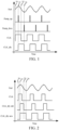
- FIG. 1 shows the timing of signals used to control a crystal oscillator ("Xtal") in switched oscillator topology from a reference clock having a 50% input duty cycle.
- a rising edge of a reference clock (“CLK”) is delayed to produce a rising edge of a delayed clock (“CLK_dly”) at 12.
- CLK_dly a rising edge of a delayed clock
- a falling edge of the clock is delayed to produce a falling edge of the delayed clock at 16.
- the rising and falling edges of the delayed clock may be used to generate short timing signals "Pump_up” and "Pump_dwn” at the crests and troughs of the crystal oscillator.
- FIG. 2 shows the timing of signals used to control a switched crystal oscillator when the reference clock has a 30% input duty cycle.
- CLK a rising edge of the reference clock
- CLK_dly old a delayed clock
- CLK_dly new a delayed clock
- the delayed clock shown by "CLK_dly old” has a falling edge at 24, in contrast to the delayed clock shown by "CLK_dly new” which has a falling edge at 26.
- the falling edge at 24 is not properly centered at a trough of the crystal oscillator, unlike the properly aligned edge at 26, which is centered at the trough and the low state of the reference clock "CLK”. Accordingly, there are advantages for crystal oscillator control as well as DDR applications and other non-limiting applications, to generating a delayed clock with both rising and falling edges properly centered within corresponding high and low states of the reference clock, from which the delayed clock is derived.
- FIG. 3 shows an embodiment 30 of a quadrature phase shifted clock generation circuit with duty cycle correction, in accordance with the present disclosure.
- a reference clock 32 is delayed by a delay circuit 34 to generate a delayed clock 36.
- An Exclusive-NOR (XNOR) logical gate 38 generates a control "Cntrl” signal 40 from the reference clock 32 and the delayed clock 36.
- the "Cntrl” signal 40 is inverted by an inverter 42 to generate a "Cntrl_b” signal 44.
- a charging and discharging circuit is configured to modify a ripple voltage 46 and is formed between a supply voltage 48 and ground 50.
- a current source 52 in series with a P-channel Field Effect Transistor (PFET) will increase the ripple voltage 46 when Cntrl 40 is in a high state.
- PFET P-channel Field Effect Transistor
- NFET N-channel Field Effect Transistor
- a second branch is formed with a PFET 60 between the current source 52 and a current source 62 and an NFET 66 between a current source 64 and the current source 58.
- the purpose of this second branch is to divert current from the current source 52 to the current source (e.g. sink) 62 when the ripple voltage 46 is not being charged through the PFET 54.
- the second branch also diverts current from the current source 64 to the current source (e.g. sink) 58 when the ripple voltage 46 is not being discharged through the NFET 56.
- the embodiment 30 may operate in an ultra-low current application where control of parasitic effects is important. An implementation based on current mirroring devices would require large transistor device sizes with correspondingly large parasitic effects. Thus, to reduce non-ideality arising from the larger parasitic effects of mirrored current devices, alternate current paths are provided rather than switching off the current sources 52 and 58.
- the ripple voltage 46 may be increased or decreased (e.g., charged or discharged) based on a first, second, third or fourth combination of the states (e.g. high or low) of the reference clock 32 and the delayed clock 36.
- the first combination reference clock 32 high and delayed clock 36 low
- the third combination reference clock 32 low and delayed clock 36 high
- the XNOR gate 38 will be decoded by the XNOR gate 38 to drive the Cntrl signal 40 low, thereby activating the PFET 54 to charge the ripple voltage 46 from the current source 52.
- the second combination (reference clock 32 high and delayed clock 36 high) and the fourth combination (reference clock 32 low and delayed clock 36 low) will result in the Cntrl signal 40 driven high and the ripple voltage 46 discharging through the NFET 56 and the current source 58.
- the charging and discharging of the ripple voltage 46 during the high state of the reference clock 32 is used to adjust and center a rising edge of the delayed clock 36 within the high state of the reference clock 32. Accordingly, during the high state of the reference clock 32, the ripple voltage 46 is allowed to pass through a transmission gate 70 to a node Vriph 72 and may be stored on a capacitor 74. The transmission gate is enabled to allow coupling of the ripple voltage 46 to the node 72 with the reference clock 32 and an inverted reference clock (“Clk_"b) 76. Similarly, the charging and discharging of the ripple voltage 46 during the low state of the reference clock 32 is used to adjust and center a falling edge of the delayed clock 36 within the low state of the reference clock 32.
- the ripple voltage 46 is allowed to pass through a transmission gate 80 to a node Vripl 82 and may be stored on a capacitor 84.
- the transmission gate is enabled to allow coupling of the ripple voltage 46 to the node 82 with the reference clock 32 and the inverted reference clock ("Clk_"b) 76.
- the value of the ripple voltage 46 subsequently stored on the respective capacitors 74 and 84 may be referred to as a respective edge value.
- the ripple voltage on the nodes Vriph 72 and Vripl 82 are alternately multiplexed and coupled to the control voltage 94 with transmission gates 90 and 96.
- the control voltage 94 is driven (by coupling) to the ripple voltage on the Vriph node 72 when the delayed clock 36 is low (e.g. Clk_dly 36 is high and Clk_dly_b 92 is low).
- the control voltage 94 is driven (by coupling) to the ripple voltage on the Vripl node 82 when the delayed clock 36 is high.
- the falling edge of the reference clock 32 is delayed by the delay circuit 34 with a fully integrated (charged) ripple voltage 46 before generating the falling edge of the delayed clock 36.
- the rising edge of the reference clock 32 is delayed by the delay circuit 34 with a fully integrated (charged) ripple voltage 46 before generating the rising edge of the delayed clock 36.
- the delay circuit 34 is initialized to provide a zero-time delay using a PFET 98 controlled by an Enable ("En") signal 100.
- the delay circuit 34 may comprise a cascaded plurality of inverters 102, whose bias current (e.g., IDS) may be sourced by a respective NFET 104 connected to ground 50. For example, increasing the control voltage 94 will result in more current sunk from the NEFT 104 to ground 50, thereby increasing the transconductance of the transistors comprising each inverter 102 and reducing the transit delay therethrough.
- the output of the delay circuit 34 may be further buffered by inverters 106 and 108 to generate the delayed clock 36.
- FIG. 4 shows the generated timing signals of the embodiment 30 of FIG. 3 with a 50% input duty cycle of the reference clock 32.
- the first combination of the states of the reference clock 32 and the delayed clock 36 is defined between a rising edge 110 of the reference clock 32 and a rising edge 112 of the delayed clock 36.
- the second combination of the states of the reference clock 32 and the delayed clock 36 is defined between the rising edge 112 of the delayed clock 36 and a falling edge 114 of the reference clock 32.
- the third combination of the states of the reference clock 32 and the delayed clock 36 is defined between the falling edge 114 of the reference clock 32 and a falling edge 116 of the delayed clock 36.
- the fourth combination of the states of the reference clock 32 and the delayed clock 36 is defined between the falling edge 116 of the delayed clock 36 and a rising edge 118 of the reference clock 32.
- the ripple voltage 46 includes both a voltage increase and decrease (e.g. charging and discharging) to center both the rising and falling edges of the delayed clock 36.
- the voltage control 94 is multiplexed between the voltages on the Vriph node 72 and the Vripl node 82 using the delayed clock 36 and the inverted delayed clock 92.
- coincident traces for the ripple voltage 46 and the control voltage 94 are offset in FIG. 4 and subsequent similar figures so that the behavior of these voltages may be more clearly visualized and understood.
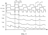
- FIG. 5 shows the generated timing signals during the initialization of embodiment 30 of FIG. 3 with a 50% input duty cycle of the reference clock 32.
- the rising edge 120 of the reference clock 32 generates a corresponding rising edge 122 of the delayed clock 36, which initially is poorly centered within the high state of the reference clock 32.
- the falling edge 124 of the reference clock 32 generates a corresponding rising edge 126 of the delayed clock 36, which initially is poorly centered within the low state of the reference clock 32.
- the closed loop system of FIG. 3 converges with both centered falling edge 130 and centered rising edge 132 of the delayed clock 36.
- FIG. 6 and FIG. 7 show the convergence of aligning rising and falling edges of the delayed clock 36 for a reference clock 32 having an input duty cycle of 25% and 75% respectively.
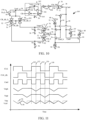
- FIG. 8 shows an embodiment 140 of a quadrature phase shifted clock generation circuit with duty cycle correction and ripple masking, in accordance with the present disclosure.
- FIG. 9 shows the generated timing signals from the embodiment 140 of FIG. 8 .
- FIG. 9 and in contrast to FIG. 3 and FIG. 4 , a ripple mask is formed in the embodiment 140 in the negative feedback loop. Specifically, the transfer of the ripple voltage 46 to the multiplexer formed by transmission gates 90 and 96 is buffered in two stages so that more stability is provided to delay circuit 34 controlled by the control voltage 94.
- the ripple voltage 46 is transferred to the Vriph node 72 during a high state of the reference clock 32, then through a transmission gate 142 to a node 144 having a storage capacitor 146 during a low state of the reference clock 32.
- the ripple voltage 46 is transferred to the Vripl node 82 during a low state of the reference clock 32, then through a transmission gate 152 to a node 154 having a storage capacitor 156 during a high state of the reference clock 32.
- control voltage 94 are preferably masked to ensure predictable delays from the rising edge 110 of the reference clock 32 to the rising edge 112 of the delayed clock 36 and from the falling edge 114 of the reference clock 32 to the falling edge 116 of the delayed clock 36.
- FIG. 10 shows an embodiment 160 of a quadrature phase shifted clock generation circuit with duty cycle correction with a PFET based delay control, in accordance with the present disclosure.
- FIG. 11 shows the corresponding generation of timing signals for the embodiment 160 of FIG. 10 .
- a delay circuit 162 is formed with a cascaded plurality of inverters 164 whose bias current (e.g., IDS) may be provided by a respective PFET 166 connect to the voltage source 48.
- IDS bias current
- decreasing the control voltage 94 will result in more current sourced from the PFET 166 from the supply 48, thereby increasing the transconductance of the transistors comprising each inverter 164 and reducing the transit delay therethrough.
- the function of the Cntrl signal 40 is also modified by generating an inverted signal Cntrl_b 44 with an inverter 43.
- the inverted signal Cntrl_b44 now drives the gates of the PFET 54 and NFET 56 respectively.
- the delay circuit 162 is initialized to provide a zero-time delay using an NFET 168 controlled by an inverted Enable (“En_b”) signal 170.
- FIG. 12 shows an embodiment 180 of a quadrature phase shifted clock generation circuit modified to control the rising edge of the delayed clock without changing duty cycle, in accordance with an embodiment of the present disclosure.
- the embodiment 180 is simplified over previously described embodiments at the expense of controlling only one edge of the delayed clock 36, while still being able to operate over a full input duty cycle range of the reference clock 32.
- FIG. 13 shows the generated timing signals from the embodiment 180 of FIG. 12 .
- a bistable device e.g.
- a "flip-flop" 182 captures various combinations of the reference clock 32 and the delayed clock 36 to generate a discharge signal ("Out_Dwn") 184, an inverted discharge signal (“Out_Dwn_b”) 186 from inverter 185, an inverted charging signal (“Out_Up_b”) 188 from a NOR gate 189 and a charging signal (“Out_Up”) 190 from an inverter 191.
- the ripple voltage 46 may be stored on a capacitor 192 and initialized with a PFET 194 controlled by the enable signal (“En”) 100.
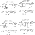
- FIG. 14 to FIG. 17 show alternative embodiments 210, 212, 214 and 216 respectively with the embodiment 210 included in the embodiment 180 of FIG. 12 .
- the embodiment 180 of FIG. 12 includes the embodiment 210 of FIG. 14 . Accordingly tg_gate 196 may be driven by Clk_Dly_b 92 and tg_gate_b 197 may be driven by Clk_Dly 36.
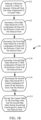
- FIG. 18 shows an embodiment 220 of a method for quadrature phase shifted clock generation with duty cycle correction.
- a reference clock 32 is delayed (by the delay circuit 34) to generate a delayed clock 36, the delay proportional to a control value 94.
- a first edge value (Vriph 72 associated with the rising edge at 112), is increased based on a first combination of states (between edges 110 and 112) of the reference clock 32 and the delayed clock 36.
- the first edge value is decreased based on a second combination of states (between edges 112 and 114).
- a second edge value (Vripl 82 associated with the falling edge at 114), is increased based on a third combination of states (between edges 114 and 116).
- the second edge value is decreased based on a fourth combination of states (between edges 116 and 118).
- the control value 94 is driven to the first edge value Vriph 72 and the second edge value Vripl 82 during second (high) and first (low) respective states of the delayed clock 36.
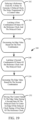
- FIG. 19 shows an embodiment 240 of a method for quadrature phase shifted clock generation with extended input duty range.
- a reference clock 32 is delayed by a delay to generate a delayed clock 36, where the delay is proportional to a control value 94.
- a first combination of states of the reference clock 32 and the delayed clock 36 is latched (with the flip-flop 182).
- an edge value 198 is decreased based on the first combination.
- a second combination of states of the reference clock 32 and the delayed clock 36 is latched (with the flip-flop 182).
- the edge value 198 is increased based on the second combination.
- the control value 94 is driven to the edge value 46 during a second state (low) state of the delayed clock 36 to center an edge 198 of the delayed clock 36 during a first state (high) of the reference clock 32.
- a method for quadrature phase shifted clock generation with duty cycle correction comprises delaying a reference clock with a delay circuit to generate a delayed clock, wherein a delay of the delay circuit is proportional to a control value, and each of the reference clock and the delayed clock comprise a plurality of states comprising a first state and a second state.
- a first edge value is increased in response to a first combination of the states of the reference clock and the delayed clock.
- the first edge value is decreased in response to a second combination of the states of the reference clock and the delayed clock.
- a second edge value is increased in response to a third combination of the states of the reference clock and the delayed clock.
- the second edge value is decreased in response to a fourth combination of the states of the reference clock and the delayed clock.
- the control value is driven to the first edge value during the second state of the delayed clock.
- the control value is driven to the second edge value during the first state of the delayed clock.
- Alternative embodiments of the method for quadrature phase shifted clock generation with duty cycle correction include one of the following features, or any combination thereof. At least one of increasing and decreasing each of the first edge value and the second edge value is responsive to changing a respective charge on a respective capacitor of the first edge value and the second edge value.
- Driving the control value comprises multiplexing one of the first edge value and the second edge value, wherein the control value controls a voltage controlled current source of the delay circuit configured to modify a bias current of a cascaded plurality of inverters between the reference clock and the delayed clock.
- Driving the control value to the first edge value further comprises decoupling the first edge value from the control value during the first state of the reference clock and driving the control value to the second edge value further comprises decoupling the second edge value from the control value during the second state of the reference clock.
- the first combination of the states comprises the first state of the reference clock and the second state of the delayed clock.
- the second combination of the states comprises the first state of the reference clock and the first state of the delayed clock.
- the third combination of the states comprises the second state of the reference clock and the first state of the delayed clock.
- the fourth combination of the states comprises the second state of the reference clock and the second state of the delayed clock.
- the method for quadrature phase shifted clock generation with duty cycle correction is applied to the delayed clock to generate a second delayed clock, and to recover a radio frequency signal with a double data rate clock formed by the delayed clock and the second delayed clock.
- an apparatus comprises a delay circuit configured to generate a delayed clock from a reference clock, wherein a first edge of the delayed clock is delayed by a first delay in response to a first control value and a second edge of the delayed clock is delayed by a second delay in response to a second control value, and wherein each of the reference clock and the delayed clock comprise a plurality of states comprising a first state and a second state.
- a first control circuit is configured to determine the first control value by increasing a first voltage for a first time interval spanning a first edge of the first state of the reference clock and the first edge of the delayed clock, and decreasing the first voltage for a second time interval spanning the second edge of the first state of the reference clock and the first edge of the delayed clock.
- a second control circuit is configured to determine the second control value by increasing a second voltage for a third time period spanning a first edge of the second state of the reference clock and a second edge of the delayed clock and decreasing the second voltage for a fourth time period spanning a second edge of the second state of the reference clock and the second edge of the delayed clock.
- a first capacitor is configured to store a first charge alterable by at least one of increasing and decreasing the first voltage
- a second capacitor is configured to store a second charge alterable by at least one of increasing and decreasing the second voltage.
- a multiplexer is configured to couple the first control value to the delay circuit in response to the second state of the delayed clock, and to couple the second control value to the delay circuit in response to the first state of the delayed clock.
- a first transmission gate is configured to decouple the first control value from a control input to the delay circuit during the first state of the reference clock and to decouple the second control value from the control input to the delay circuit during the second state of the reference clock.
- the delay circuit comprises a cascaded plurality of inverters between the reference clock and the delayed clock, and at least two of the invertors comprise a bias current responsive to the first control value and the second control value.
- the bias current is sourced by a N-channel Field Effect Transistor and the first delay and the second delay are each inversely proportional to the control input to the delay circuit.
- the bias current is sourced by a P-channel Field Effect Transistor and the first delay and the second delay are each proportional to the control input to the delay circuit.
- the delayed clock from the apparatus is coupled to a second instance of the apparatus to generate a second delayed clock, wherein the delayed clock and the second delayed clock each are duty cycle corrected and are combined to form a double data rate clock having twice the frequency of the reference clock.
- a method for quadrature phase shifted clock generation with extended input duty range comprises delaying a reference clock with a delay circuit to generate a delayed clock, wherein a delay of the delay circuit is proportional to a control value, and each of the reference clock and the delayed clock comprise a plurality of states comprising a first state and a second state.
- a first combination of the respective states of the reference clock and the delayed clock is latched.
- An edge value is decreased in response to the first combination of the respective states of the reference clock and the delayed clock.
- a second combination of the respective states of the reference clock and the delayed clock is latched.
- the edge value is increased in response to the second combination of the respective states of the reference clock and the delayed clock.
- the control value is driven to the edge value during the second state of the delayed clock to center an edge of the delayed clock during the first state of the reference clock.
- Alternative embodiments of the method for quadrature phase shifted clock generation with extended input duty range include one of the following features, or any combination thereof.
- the edge value is increased in response to a first signal determined by a logical OR function of a transmission gating signal and an output of a latch configured to latch the first combination and the second combination, wherein the transmission gating signal is used to couple the edge value to the control value during the second state of the delayed clock.
Landscapes
- Physics & Mathematics (AREA)
- Nonlinear Science (AREA)
- Engineering & Computer Science (AREA)
- Theoretical Computer Science (AREA)
- General Engineering & Computer Science (AREA)
- General Physics & Mathematics (AREA)
- Pulse Circuits (AREA)
Abstract
Description
- This disclosure relates generally to electronic circuits, and more specifically to the generation of a quadrature phase shifted clock from a reference clock having an arbitrary input
duty cycle. - In switched crystal oscillator circuits, timing the charging and discharging of crystal nodes at exactly their maxima and minima is important for efficient operation and to minimize power consumption. Accordingly, it is advantageous to delay both edges of a delayed clock to
be properly centered with respect to a respective high or low phase of a reference clock, from which the delayed clock is derived. Furthermore, the timing of the edges of the delayed clock should not be sensitive to changes in the duty cycle of the reference clock. - Many high-speed circuits and logic families use double data rate technology, where both rising and falling edges of the delayed clock may be used to trigger different events. In
addition, with respect to the use of high frequency clocks, symmetry between high time and low time is desired to minimize constraints on set-up & hold timings, arising from non-ideal input duty cycle and to allow proper functioning at higher frequencies. - The present invention is illustrated by way of example and is not limited by the accompanying figures, in which like references indicate similar elements. Elements in the figures are illustrated for simplicity and clarity and have not necessarily been drawn to scale.
-
FIG. 1 is a graphical view of generated timing signals from an embodiment of clock delay circuit having an input reference clock with a 50% input duty cycle. -
FIG. 2 is a graphical view of generated timing signals from an embodiment of clock delay circuit having an input reference clock with a 30% input duty cycle. -
FIG. 3 is a schematic view of a quadrature phase shifted clock generation circuit with duty cycle correction, in accordance with an embodiment of the present disclosure. -
FIG. 4 is a graphical view of generated timing signals from the embodiment ofFIG. 3 using an input reference clock with a 50% input duty cycle. -
FIG. 5 is a graphical view of generated timing signals during initialization of the embodiment ofFIG. 3 using an input reference clock with a 50% input duty cycle. -
FIG. 6 is a graphical view of generated timing signals from the embodiment ofFIG. 3 using an input reference clock with a 25% input duty cycle. -
FIG. 7 is a graphical view of generated timing signals from the embodiment ofFIG. 3 using an input reference clock with a 75% input duty cycle. -
FIG. 8 is a schematic view of a quadrature phase shifted clock generation circuit with ripple masking, in accordance with an embodiment of the present disclosure. -
FIG. 9 is a graphical view of generated timing signals from the embodiment ofFIG. 8 using an input reference clock with a 50% input duty cycle. -
FIG. 10 is a schematic view of the quadrature phase shifted clock generation circuit ofFIG. 3 with a modified delay line, in accordance with an embodiment of the present disclosure. -
FIG. 11 is a graphical view of generated timing signals from the embodiment ofFIG. 10 using an input reference clock with a 50% input duty cycle. -
FIG. 12 is a schematic view of a quadrature phase shifted clock generation circuit modified to control only one edge of the delayed clock, in accordance with an embodiment of the present disclosure. -
FIG. 13 is a graphical view of generated timing signals from the embodiment ofFIG. 12 using an input reference clock with a 50% input duty cycle. -
FIG. 14 to FIG. 17 are schematic views of alternative embodiments modifying the embodiment ofFIG. 12 , in accordance with an embodiment of the present disclosure. -
FIG. 18 is a flowchart representation of a method for quadrature phase shifted clock generation with duty cycle correction, in accordance with an embodiment of the present disclosure. -
FIG. 19 is a flowchart representation of another method for quadrature phase shifted clock generation with extended input duty range, in accordance with an embodiment of the present disclosure. - Embodiments described herein provide for the centering and alignment of one or both edges of a delayed clock relative to a reference clock used to derive the delayed clock. Edge alignment is achieved over an entire input duty range of the reference clock by using a feedback loop that adjusts the edge by determining a control value. The control value may be determined from a combination of charging and discharging a capacitor, by integrating an inductive current or by other methods used to determine a measure of elapsed time between the edge of the delayed clock and the beginning and end of a high state or low state of the reference clock, from which the delayed clock is derived. By further determining a difference between the elapsed time and the edges of the reference clock, a rising edge of the delayed clock may be adjusted to be centered between logic high state of reference clock (or similarly for the corresponding fall edges of the delayed and reference clocks). Centering of the edges may be achieved within limits of environmental and manufacturing tolerances of an apparatus used to achieve the same.
-
FIG. 1 shows the timing of signals used to control a crystal oscillator ("Xtal") in switched oscillator topology from a reference clock having a 50% input duty cycle. At 10, a rising edge of a reference clock ("CLK") is delayed to produce a rising edge of a delayed clock ("CLK_dly") at 12. Similarly, at 14, a falling edge of the clock is delayed to produce a falling edge of the delayed clock at 16. The rising and falling edges of the delayed clock may be used to generate short timing signals "Pump_up" and "Pump_dwn" at the crests and troughs of the crystal oscillator. - In contrast to
FIG. 1, FIG. 2 shows the timing of signals used to control a switched crystal oscillator when the reference clock has a 30% input duty cycle. At 20, a rising edge of the reference clock ("CLK") may be used to generate a delayed clock (CLK_dly old or CLK_dly new) with a rising edge at 22, properly centered within a high state of the reference clock. The delayed clock shown by "CLK_dly old" has a falling edge at 24, in contrast to the delayed clock shown by "CLK_dly new" which has a falling edge at 26. The falling edge at 24 is not properly centered at a trough of the crystal oscillator, unlike the properly aligned edge at 26, which is centered at the trough and the low state of the reference clock "CLK". Accordingly, there are advantages for crystal oscillator control as well as DDR applications and other non-limiting applications, to generating a delayed clock with both rising and falling edges properly centered within corresponding high and low states of the reference clock, from which the delayed clock is derived. -
FIG. 3 shows anembodiment 30 of a quadrature phase shifted clock generation circuit with duty cycle correction, in accordance with the present disclosure. Areference clock 32 is delayed by adelay circuit 34 to generate adelayed clock 36. An Exclusive-NOR (XNOR)logical gate 38 generates a control "Cntrl"signal 40 from thereference clock 32 and thedelayed clock 36. The "Cntrl"signal 40 is inverted by aninverter 42 to generate a "Cntrl_b"signal 44. A charging and discharging circuit is configured to modify aripple voltage 46 and is formed between asupply voltage 48 andground 50. Acurrent source 52 in series with a P-channel Field Effect Transistor (PFET) will increase theripple voltage 46 whenCntrl 40 is in a high state. Conversely, an N-channel Field Effect Transistor (NFET) 56 in series with acurrent source 58 will discharge theripple voltage 46 whenCntrl 40 is in a low state. - A second branch is formed with a
PFET 60 between thecurrent source 52 and acurrent source 62 and an NFET 66 between acurrent source 64 and thecurrent source 58. The purpose of this second branch is to divert current from thecurrent source 52 to the current source (e.g. sink) 62 when theripple voltage 46 is not being charged through thePFET 54. Conversely, the second branch also diverts current from thecurrent source 64 to the current source (e.g. sink) 58 when theripple voltage 46 is not being discharged through theNFET 56. Theembodiment 30 may operate in an ultra-low current application where control of parasitic effects is important. An implementation based on current mirroring devices would require large transistor device sizes with correspondingly large parasitic effects. Thus, to reduce non-ideality arising from the larger parasitic effects of mirrored current devices, alternate current paths are provided rather than switching off thecurrent sources - The
ripple voltage 46 may be increased or decreased (e.g., charged or discharged) based on a first, second, third or fourth combination of the states (e.g. high or low) of thereference clock 32 and thedelayed clock 36. In one embodiment, the first combination (reference clock 32 high anddelayed clock 36 low), and the third combination (reference clock 32 low anddelayed clock 36 high) will be decoded by the XNORgate 38 to drive theCntrl signal 40 low, thereby activating thePFET 54 to charge theripple voltage 46 from thecurrent source 52. Conversely, the second combination (reference clock 32 high anddelayed clock 36 high) and the fourth combination (reference clock 32 low anddelayed clock 36 low) will result in theCntrl signal 40 driven high and theripple voltage 46 discharging through theNFET 56 and thecurrent source 58. - In one embodiment, the charging and discharging of the
ripple voltage 46 during the high state of thereference clock 32 is used to adjust and center a rising edge of thedelayed clock 36 within the high state of thereference clock 32. Accordingly, during the high state of thereference clock 32, theripple voltage 46 is allowed to pass through atransmission gate 70 to a node Vriph 72 and may be stored on acapacitor 74. The transmission gate is enabled to allow coupling of theripple voltage 46 to thenode 72 with thereference clock 32 and an inverted reference clock ("Clk_"b) 76. Similarly, the charging and discharging of theripple voltage 46 during the low state of thereference clock 32 is used to adjust and center a falling edge of thedelayed clock 36 within the low state of thereference clock 32. Accordingly, during the low state of thereference clock 32, theripple voltage 46 is allowed to pass through atransmission gate 80 to anode Vripl 82 and may be stored on acapacitor 84. The transmission gate is enabled to allow coupling of theripple voltage 46 to thenode 82 with thereference clock 32 and the inverted reference clock ("Clk_"b) 76. In some embodiments, the value of theripple voltage 46 subsequently stored on therespective capacitors 74 and 84 (e.g.,Vriph 72 and Vripl 82), may be referred to as a respective edge value. - The ripple voltage on the nodes Vriph 72 and
Vripl 82 are alternately multiplexed and coupled to thecontrol voltage 94 withtransmission gates control voltage 94 is driven (by coupling) to the ripple voltage on theVriph node 72 when the delayedclock 36 is low (e.g.Clk_dly 36 is high andClk_dly_b 92 is low). Thecontrol voltage 94 is driven (by coupling) to the ripple voltage on theVripl node 82 when the delayedclock 36 is high. In so doing, the falling edge of thereference clock 32 is delayed by thedelay circuit 34 with a fully integrated (charged)ripple voltage 46 before generating the falling edge of the delayedclock 36. Similarly, the rising edge of thereference clock 32 is delayed by thedelay circuit 34 with a fully integrated (charged)ripple voltage 46 before generating the rising edge of the delayedclock 36. - In one embodiment, the
delay circuit 34 is initialized to provide a zero-time delay using aPFET 98 controlled by an Enable ("En")signal 100. Thedelay circuit 34 may comprise a cascaded plurality ofinverters 102, whose bias current (e.g., IDS) may be sourced by arespective NFET 104 connected to ground 50. For example, increasing thecontrol voltage 94 will result in more current sunk from theNEFT 104 to ground 50, thereby increasing the transconductance of the transistors comprising eachinverter 102 and reducing the transit delay therethrough. In one embodiment, the output of thedelay circuit 34 may be further buffered byinverters clock 36. -
FIG. 4 shows the generated timing signals of theembodiment 30 ofFIG. 3 with a 50% input duty cycle of thereference clock 32. Specifically, the first combination of the states of thereference clock 32 and the delayedclock 36 is defined between a risingedge 110 of thereference clock 32 and a risingedge 112 of the delayedclock 36. The second combination of the states of thereference clock 32 and the delayedclock 36 is defined between the risingedge 112 of the delayedclock 36 and a fallingedge 114 of thereference clock 32. The third combination of the states of thereference clock 32 and the delayedclock 36 is defined between the fallingedge 114 of thereference clock 32 and a fallingedge 116 of the delayedclock 36. The fourth combination of the states of thereference clock 32 and the delayedclock 36 is defined between the fallingedge 116 of the delayedclock 36 and a risingedge 118 of thereference clock 32. As discussed with the reference toFIG. 3 , theripple voltage 46 includes both a voltage increase and decrease (e.g. charging and discharging) to center both the rising and falling edges of the delayedclock 36. Thevoltage control 94 is multiplexed between the voltages on theVriph node 72 and theVripl node 82 using the delayedclock 36 and the inverted delayedclock 92. For ease of illustration, coincident traces for theripple voltage 46 and thecontrol voltage 94 are offset inFIG. 4 and subsequent similar figures so that the behavior of these voltages may be more clearly visualized and understood. -
FIG. 5 with continued reference toFIG. 3 shows the generated timing signals during the initialization ofembodiment 30 ofFIG. 3 with a 50% input duty cycle of thereference clock 32. As shown inFIG. 5 , the risingedge 120 of thereference clock 32 generates a corresponding risingedge 122 of the delayedclock 36, which initially is poorly centered within the high state of thereference clock 32. Similarly, the fallingedge 124 of thereference clock 32 generates a corresponding risingedge 126 of the delayedclock 36, which initially is poorly centered within the low state of thereference clock 32. After several cycles, the closed loop system ofFIG. 3 converges with both centered fallingedge 130 and centered risingedge 132 of the delayedclock 36. Similarly,FIG. 6 and FIG. 7 show the convergence of aligning rising and falling edges of the delayedclock 36 for areference clock 32 having an input duty cycle of 25% and 75% respectively. -
FIG. 8 shows anembodiment 140 of a quadrature phase shifted clock generation circuit with duty cycle correction and ripple masking, in accordance with the present disclosure.FIG. 9 shows the generated timing signals from theembodiment 140 ofFIG. 8 . With reference toFIG. 8, FIG. 9 and in contrast toFIG. 3 andFIG. 4 , a ripple mask is formed in theembodiment 140 in the negative feedback loop. Specifically, the transfer of theripple voltage 46 to the multiplexer formed bytransmission gates circuit 34 controlled by thecontrol voltage 94. Specifically, theripple voltage 46 is transferred to theVriph node 72 during a high state of thereference clock 32, then through atransmission gate 142 to anode 144 having astorage capacitor 146 during a low state of thereference clock 32. Similarly, theripple voltage 46 is transferred to theVripl node 82 during a low state of thereference clock 32, then through atransmission gate 152 to anode 154 having astorage capacitor 156 during a high state of thereference clock 32. While the closed loop system ofembodiment 140 may ensure proper edge centering, variation in thecontrol voltage 94 are preferably masked to ensure predictable delays from the risingedge 110 of thereference clock 32 to the risingedge 112 of the delayedclock 36 and from the fallingedge 114 of thereference clock 32 to the fallingedge 116 of the delayedclock 36. -
FIG. 10 shows anembodiment 160 of a quadrature phase shifted clock generation circuit with duty cycle correction with a PFET based delay control, in accordance with the present disclosure.FIG. 11 shows the corresponding generation of timing signals for theembodiment 160 ofFIG. 10 . - With reference to
FIG. 10, FIG. 11 and in contrast toFIG. 3 andFIG. 4 , adelay circuit 162 is formed with a cascaded plurality ofinverters 164 whose bias current (e.g., IDS) may be provided by arespective PFET 166 connect to thevoltage source 48. For example, decreasing thecontrol voltage 94 will result in more current sourced from thePFET 166 from thesupply 48, thereby increasing the transconductance of the transistors comprising eachinverter 164 and reducing the transit delay therethrough. The function of theCntrl signal 40 is also modified by generating aninverted signal Cntrl_b 44 with aninverter 43. The inverted signal Cntrl_b44 now drives the gates of thePFET 54 andNFET 56 respectively. In one embodiment, thedelay circuit 162 is initialized to provide a zero-time delay using anNFET 168 controlled by an inverted Enable ("En_b")signal 170. -
FIG. 12 shows anembodiment 180 of a quadrature phase shifted clock generation circuit modified to control the rising edge of the delayed clock without changing duty cycle, in accordance with an embodiment of the present disclosure. Theembodiment 180 is simplified over previously described embodiments at the expense of controlling only one edge of the delayedclock 36, while still being able to operate over a full input duty cycle range of thereference clock 32.FIG. 13 shows the generated timing signals from theembodiment 180 ofFIG. 12 . Referring toFIG. 12 and FIG. 13 , a bistable device (e.g. a "flip-flop") 182 captures various combinations of thereference clock 32 and the delayedclock 36 to generate a discharge signal ("Out_Dwn") 184, an inverted discharge signal ("Out_Dwn_b") 186 frominverter 185, an inverted charging signal ("Out_Up_b") 188 from a NORgate 189 and a charging signal ("Out_Up") 190 from aninverter 191. In addition, in one embodiment theripple voltage 46 may be stored on acapacitor 192 and initialized with aPFET 194 controlled by the enable signal ("En") 100. - In steady state, when both the
reference clock 32 and the delayedclock 36 are in a high state, the discharge signal ("Out_Dwn") 184 is in a high state and theripple voltage 46 discharges with a constant current set by thecurrent source 58. When thereference clock 32 transitions low (at 199), the flip-flop 182 is reset and the Out_Dwn signal 184 transitions low. When thereference clock 32 is low and the delayedclock 36 is high, theOut_Up signal 190 goes low and theripple voltage 46 then charges with a constant current defined by thecurrent source 52. When the delayedclock 36 is low (betweenedges 199 and 200), both charging and discharging is disabled, hence theripple voltage 46 is stable and thetransmission gate 195 is opened (with a high value ontg_gate 196 and a low value on tg_gate_b 197) thus shorting theripple voltage 46 to thecontrol voltage 94. Accordingly, theripple voltage 46 is discharged from a risingedge 198 of the delayedclock 36 to the fallingedge 199 of thereference clock 32 and charged from the fallingedge 199 of thereference clock 32 to the fallingedge 200 of the delayedclock 36.FIG. 14 to FIG. 17 showalternative embodiments embodiment 210 included in theembodiment 180 ofFIG. 12 . Theembodiment 180 ofFIG. 12 includes theembodiment 210 ofFIG. 14 . Accordingly tg_gate 196 may be driven byClk_Dly_b 92 andtg_gate_b 197 may be driven byClk_Dly 36. -
FIG. 18 shows anembodiment 220 of a method for quadrature phase shifted clock generation with duty cycle correction. With reference toFIG. 3 ,FIG. 4 andFIG. 18 , at 222 areference clock 32 is delayed (by the delay circuit 34) to generate a delayedclock 36, the delay proportional to acontrol value 94. At 224, a first edge value (Vriph 72 associated with the rising edge at 112), is increased based on a first combination of states (betweenedges 110 and 112) of thereference clock 32 and the delayedclock 36. At 226, the first edge value is decreased based on a second combination of states (betweenedges 112 and 114). At 228, a second edge value (Vripl 82 associated with the falling edge at 114), is increased based on a third combination of states (betweenedges 114 and 116). At 230, the second edge value is decreased based on a fourth combination of states (betweenedges 116 and 118). At 232, thecontrol value 94 is driven to the firstedge value Vriph 72 and the secondedge value Vripl 82 during second (high) and first (low) respective states of the delayedclock 36. -
FIG. 19 shows anembodiment 240 of a method for quadrature phase shifted clock generation with extended input duty range. With reference toFIG. 12, FIG. 13 andFIG. 19 , at 242 areference clock 32 is delayed by a delay to generate a delayedclock 36, where the delay is proportional to acontrol value 94. At 244, a first combination of states of thereference clock 32 and the delayedclock 36 is latched (with the flip-flop 182). At 246, anedge value 198 is decreased based on the first combination. At 248, a second combination of states of thereference clock 32 and the delayedclock 36 is latched (with the flip-flop 182). At 250, theedge value 198 is increased based on the second combination. At 252, thecontrol value 94 is driven to theedge value 46 during a second state (low) state of the delayedclock 36 to center anedge 198 of the delayedclock 36 during a first state (high) of thereference clock 32. - As will be appreciated, at least some of the embodiments as disclosed include at least the following. In one embodiment, a method for quadrature phase shifted clock generation with duty cycle correction comprises delaying a reference clock with a delay circuit to generate a delayed clock, wherein a delay of the delay circuit is proportional to a control value, and each of the reference clock and the delayed clock comprise a plurality of states comprising a first state and a second state. A first edge value is increased in response to a first combination of the states of the reference clock and the delayed clock. The first edge value is decreased in response to a second combination of the states of the reference clock and the delayed clock. A second edge value is increased in response to a third combination of the states of the reference clock and the delayed clock. The second edge value is decreased in response to a fourth combination of the states of the reference clock and the delayed clock. The control value is driven to the first edge value during the second state of the delayed clock. The control value is driven to the second edge value during the first state of the delayed clock.
- Alternative embodiments of the method for quadrature phase shifted clock generation with duty cycle correction include one of the following features, or any combination thereof. At least one of increasing and decreasing each of the first edge value and the second edge value is responsive to changing a respective charge on a respective capacitor of the first edge value and the second edge value. Driving the control value comprises multiplexing one of the first edge value and the second edge value, wherein the control value controls a voltage controlled current source of the delay circuit configured to modify a bias current of a cascaded plurality of inverters between the reference clock and the delayed clock. Driving the control value to the first edge value further comprises decoupling the first edge value from the control value during the first state of the reference clock and driving the control value to the second edge value further comprises decoupling the second edge value from the control value during the second state of the reference clock. The first combination of the states comprises the first state of the reference clock and the second state of the delayed clock. The second combination of the states comprises the first state of the reference clock and the first state of the delayed clock. The third combination of the states comprises the second state of the reference clock and the first state of the delayed clock. The fourth combination of the states comprises the second state of the reference clock and the second state of the delayed clock. The method for quadrature phase shifted clock generation with duty cycle correction is applied to the delayed clock to generate a second delayed clock, and to recover a radio frequency signal with a double data rate clock formed by the delayed clock and the second delayed clock.
- In another embodiment, an apparatus comprises a delay circuit configured to generate a delayed clock from a reference clock, wherein a first edge of the delayed clock is delayed by a first delay in response to a first control value and a second edge of the delayed clock is delayed by a second delay in response to a second control value, and wherein each of the reference clock and the delayed clock comprise a plurality of states comprising a first state and a second state. A first control circuit is configured to determine the first control value by increasing a first voltage for a first time interval spanning a first edge of the first state of the reference clock and the first edge of the delayed clock, and decreasing the first voltage for a second time interval spanning the second edge of the first state of the reference clock and the first edge of the delayed clock. A second control circuit is configured to determine the second control value by increasing a second voltage for a third time period spanning a first edge of the second state of the reference clock and a second edge of the delayed clock and decreasing the second voltage for a fourth time period spanning a second edge of the second state of the reference clock and the second edge of the delayed clock.
- Alternative embodiments of the apparatus include one of the following features, or any combination thereof. A first capacitor is configured to store a first charge alterable by at least one of increasing and decreasing the first voltage, and a second capacitor is configured to store a second charge alterable by at least one of increasing and decreasing the second voltage. A multiplexer is configured to couple the first control value to the delay circuit in response to the second state of the delayed clock, and to couple the second control value to the delay circuit in response to the first state of the delayed clock. A first transmission gate is configured to decouple the first control value from a control input to the delay circuit during the first state of the reference clock and to decouple the second control value from the control input to the delay circuit during the second state of the reference clock. The delay circuit comprises a cascaded plurality of inverters between the reference clock and the delayed clock, and at least two of the invertors comprise a bias current responsive to the first control value and the second control value. The bias current is sourced by a N-channel Field Effect Transistor and the first delay and the second delay are each inversely proportional to the control input to the delay circuit. The bias current is sourced by a P-channel Field Effect Transistor and the first delay and the second delay are each proportional to the control input to the delay circuit. The delayed clock from the apparatus is coupled to a second instance of the apparatus to generate a second delayed clock, wherein the delayed clock and the second delayed clock each are duty cycle corrected and are combined to form a double data rate clock having twice the frequency of the reference clock.
- In another embodiment, a method for quadrature phase shifted clock generation with extended input duty range comprises delaying a reference clock with a delay circuit to generate a delayed clock, wherein a delay of the delay circuit is proportional to a control value, and each of the reference clock and the delayed clock comprise a plurality of states comprising a first state and a second state. A first combination of the respective states of the reference clock and the delayed clock is latched. An edge value is decreased in response to the first combination of the respective states of the reference clock and the delayed clock. A second combination of the respective states of the reference clock and the delayed clock is latched. The edge value is increased in response to the second combination of the respective states of the reference clock and the delayed clock. The control value is driven to the edge value during the second state of the delayed clock to center an edge of the delayed clock during the first state of the reference clock.
- Alternative embodiments of the method for quadrature phase shifted clock generation with extended input duty range include one of the following features, or any combination thereof. The edge value is increased in response to a first signal determined by a logical OR function of a transmission gating signal and an output of a latch configured to latch the first combination and the second combination, wherein the transmission gating signal is used to couple the edge value to the control value during the second state of the delayed clock.
- Although the invention is described herein with reference to specific embodiments, various modifications and changes can be made without departing from the scope of the present invention as set forth in the claims below. Accordingly, the specification and figures are to be regarded in an illustrative rather than a restrictive sense, and all such modifications are intended to be included within the scope of the present invention. Any benefits, advantages, or solutions to problems that are described herein with regard to specific embodiments are not intended to be construed as a critical, required, or essential feature or element of any or all the claims.
- Unless stated otherwise, terms such as "first" and "second" are used to arbitrarily distinguish between the elements such terms describe. Thus, these terms are not necessarily intended to indicate temporal or other prioritization of such elements.
Claims (15)
- An apparatus comprising:a delay circuit configured to generate a delayed clock from a reference clock, wherein a first edge of the delayed clock is delayed by a first delay in response to a first control value and a second edge of the delayed clock is delayed by a second delay in response to a second control value, and wherein each of the reference clock and the delayed clock comprise a plurality of states comprising a first state and a second state;a first control circuit configured to determine the first control value by increasing a first voltage for a first time interval spanning a first edge of the first state of the reference clock and the first edge of the delayed clock, and decreasing the first voltage for a second time interval spanning the second edge of the first state of the reference clock and the first edge of the delayed clock; anda second control circuit configured to determine the second control value by increasing a second voltage for a third time period spanning a first edge of the second state of the reference clock and a second edge of the delayed clock and decreasing the second voltage for a fourth time period spanning a second edge of the second state of the reference clock and the second edge of the delayed clock.
- The apparatus of claim 1 further comprising a first capacitor configured to store a first charge alterable by at least one of increasing and decreasing the first voltage, and a second capacitor configured to store a second charge alterable by at least one of increasing and decreasing the second voltage.
- The apparatus of claim 1 or 2 further comprising a multiplexer configured to couple the first control value to the delay circuit in response to the second state of the delayed clock, and to couple the second control value to the delay circuit in response to the first state of the delayed clock.
- The apparatus of any claim of claims 1 to 3 further comprising a first transmission gate configured to decouple the first control value from a control input to the delay circuit during the first
state of the reference clock and to decouple the second control value from the control input to the delay circuit during the second state of the reference clock. - The apparatus of any claim of claims 1 to 4 wherein the delay circuit comprises a cascaded plurality of inverters between the reference clock and the delayed clock,
and at least two of the invertors comprise a bias current responsive to the first control value and the second control value. - The apparatus of claim 5 wherein the bias current is sourced by a N-channel Field Effect Transistor and the first delay and the second delay are each inversely proportional to the control input to the delay circuit.
- The apparatus of claim 5 or 6 wherein the bias current is sourced by a P-channel Field Effect Transistor and the first delay and the second delay are each proportional to the control input to the delay circuit.
- The apparatus of any claim of claims 1 to 7 further comprising coupling the delayed clock from the apparatus to a second instance of the apparatus to generate a second delayed clock, wherein the delayed clock and the second delayed clock each are duty cycle corrected and are combined to form a double data rate clock having twice the frequency of the reference clock.
- A method for quadrature phase shifted clock generation with duty cycle correction comprising:delaying a reference clock with a delay circuit to generate a delayed clock, wherein a delay of the delay circuit is proportional to a control value, and each of the reference clock and the delayed clock comprise a plurality of states comprising a first state and a second state;increasing a first edge value in response to a first combination of the states of the reference clock and the delayed clock;decreasing the first edge value in response to a second combination of the states of the reference clock and the delayed clock;increasing a second edge value in response to a third combination of the states of the reference clock and the delayed clock;decreasing the second edge value in response to a fourth combination of the states of the reference clock and the delayed clock;driving the control value to the first edge value during the second state of the delayed clock; anddriving the control value to the second edge value during the first state of the delayed clock.
- The method of claim 9 wherein at least one of increasing and decreasing each of the first edge value and the second edge value is responsive to changing a respective charge on a respective capacitor of the first edge value and the second edge value.
- The method of claim 9 or 10 wherein driving the control value comprises multiplexing one of the first edge value and the second edge value, wherein the control value controls a voltage controlled current source of the delay circuit configured to modify a bias current of a cascaded plurality of inverters between the reference clock and the delayed clock.
- The method of any claim of claims 9 to 11 wherein driving the control value to the first edge value further comprises decoupling the first edge value from the control value during the first state of the reference clock and driving the control value to the second edge value further comprises decoupling the second edge value from the control value during the second state of the reference clock.
- The method of any claim of claims 9 to 12 wherein the first combination of the states comprises the first state of the reference clock and the second state of the delayed clock.
- The method of any claim of claims 9 to 13 wherein the second combination of the states comprises the first state of the reference clock and the first state of the delayed clock.
- The method of any claim of claims 9 to 14 wherein the third combination of the states comprises the second state of the reference clock and the first state of the delayed clock.
Applications Claiming Priority (1)
| Application Number | Priority Date | Filing Date | Title |
|---|---|---|---|
| IN202311053451 | 2023-08-09 |
Publications (2)
| Publication Number | Publication Date |
|---|---|
| EP4507196A2 true EP4507196A2 (en) | 2025-02-12 |
| EP4507196A3 EP4507196A3 (en) | 2025-02-26 |
Family
ID=92106953
Family Applications (1)
| Application Number | Title | Priority Date | Filing Date |
|---|---|---|---|
| EP24191118.9A Pending EP4507196A3 (en) | 2023-08-09 | 2024-07-26 | Quadrature phase shifted clock generation with duty cycle correction |
Country Status (3)
| Country | Link |
|---|---|
| US (1) | US12609679B2 (en) |
| EP (1) | EP4507196A3 (en) |
| CN (1) | CN119483553A (en) |
Families Citing this family (1)
| Publication number | Priority date | Publication date | Assignee | Title |
|---|---|---|---|---|
| US12609679B2 (en) * | 2023-08-09 | 2026-04-21 | Nxp B.V. | Quadrature phase shifted clock generation with duty cycle correction |
Family Cites Families (20)
| Publication number | Priority date | Publication date | Assignee | Title |
|---|---|---|---|---|
| US5399995A (en) | 1994-04-08 | 1995-03-21 | Raytheon Company | CMOS circuit providing 90 degree phase delay |
| US5687202A (en) | 1995-04-24 | 1997-11-11 | Cyrix Corporation | Programmable phase shift clock generator |
| US5923621A (en) | 1995-06-07 | 1999-07-13 | Cirrus Logic, Inc. | Clock doubler circuit with duty cycle control |
| DE69808611T2 (en) * | 1998-07-30 | 2003-02-06 | Stmicroelectronics S.R.L., Agrate Brianza | Frequency doubler with 50% duty cycle at the output |
| FR2783649B1 (en) | 1998-09-17 | 2000-11-17 | St Microelectronics Sa | CIRCUIT FOR FILTERING A CLOCK SIGNAL |
| US6285226B1 (en) | 1999-10-25 | 2001-09-04 | Xilinx, Inc. | Duty cycle correction circuit and method |
| US6690223B1 (en) | 2001-12-27 | 2004-02-10 | Bay Microsystems, Inc. | System and method for shifting the phase of a clock signal |
| US20030179842A1 (en) * | 2002-03-22 | 2003-09-25 | Kane Michael G. | Digital pattern sequence generator |
| TW200427224A (en) * | 2003-05-21 | 2004-12-01 | Myson Century Inc | Clock multiplier |
| US6967508B2 (en) * | 2004-03-04 | 2005-11-22 | Texas Instruments Incorporated | Compact frequency doubler/multiplier circuitry |
| US7332947B2 (en) | 2005-03-15 | 2008-02-19 | Intel Corporation | Method and apparatus for distorting duty cycle of a clock |
| US7724100B2 (en) | 2007-01-31 | 2010-05-25 | Infineon Technologies Austria Ag | Oscillator structure |
| US7683683B1 (en) * | 2007-08-06 | 2010-03-23 | Marvell International Ltd. | Frequency doubler with duty-cycle correction and associated methods |
| US7576584B2 (en) | 2007-12-14 | 2009-08-18 | Analog Devices, Inc. | Clock generators for generation of in-phase and quadrature clock signals |
| US8248130B2 (en) | 2010-05-25 | 2012-08-21 | Freescale Semiconductor, Inc. | Duty cycle correction circuit |
| US9124250B2 (en) * | 2013-07-30 | 2015-09-01 | Qualcomm Incorporated | Clock doubler including duty cycle correction |
| KR101591679B1 (en) * | 2014-08-04 | 2016-02-05 | 서울대학교산학협력단 | Delay-Locked Loop Based Forwarded Clock Receiver |
| WO2021092601A2 (en) | 2020-09-25 | 2021-05-14 | Futurewei Technologies, Inc. | Techniques for calibrating 50% duty cycle differential frequency doubler |
| US12164326B2 (en) | 2022-12-09 | 2024-12-10 | Nxp B.V. | Phase shifted clock generator |
| US12609679B2 (en) * | 2023-08-09 | 2026-04-21 | Nxp B.V. | Quadrature phase shifted clock generation with duty cycle correction |
-
2024
- 2024-07-12 US US18/771,327 patent/US12609679B2/en active Active
- 2024-07-26 EP EP24191118.9A patent/EP4507196A3/en active Pending
- 2024-08-09 CN CN202411091942.5A patent/CN119483553A/en active Pending
Also Published As
| Publication number | Publication date |
|---|---|
| US20250055446A1 (en) | 2025-02-13 |
| CN119483553A (en) | 2025-02-18 |
| EP4507196A3 (en) | 2025-02-26 |
| US12609679B2 (en) | 2026-04-21 |
Similar Documents
| Publication | Publication Date | Title |
|---|---|---|
| US6369660B1 (en) | Circuit and method for preventing runaway in a phase lock loop | |
| US7199634B2 (en) | Duty cycle correction circuits suitable for use in delay-locked loops and methods of correcting duty cycles of periodic signals | |
| US20080180144A1 (en) | Phase detector circuit and method therefor | |
| US10763833B2 (en) | Multiphase oscillator circuit | |
| US6573775B2 (en) | Integrated circuit flip-flops that utilize master and slave latched sense amplifiers | |
| US6731147B2 (en) | Method and architecture for self-clocking digital delay locked loop | |
| US20170324402A1 (en) | Power efficient high speed latch circuits and systems | |
| US12609679B2 (en) | Quadrature phase shifted clock generation with duty cycle correction | |
| KR100724559B1 (en) | Level shifter | |
| US20070165476A1 (en) | Clock signal generating circuit | |
| EP2916441B1 (en) | Charge pump circuit | |
| EP1777818A1 (en) | Master-slave flip-flop, trigger flip-flop and counter | |
| US12308846B2 (en) | Clock generation circuit and voltage generation circuit including the clock generation circuit | |
| EP4383569A1 (en) | Phase shifted clock generator | |
| US20100013535A1 (en) | Latch circuit | |
| US6861911B2 (en) | Self-regulating voltage controlled oscillator | |
| US6900684B2 (en) | Pulse processing circuit and frequency multiplier circuit | |
| KR100800143B1 (en) | Phase locked loop and phase locked method | |
| CN105306017B (en) | Signal generating circuit and work period adjustment circuit | |
| JPH0629835A (en) | Loop type phase adjusting circuit | |
| JP3033719B2 (en) | Low power semiconductor integrated circuit | |
| US20080258782A1 (en) | Oscillating divider topology | |
| US12418279B2 (en) | Low power voltage controllable oscillator with rail-to-rail output | |
| CN121791858A (en) | High-speed level conversion circuit applied to phase-locked loop and phase-locked loop | |
| KR100349688B1 (en) | Lock Detector of Phase Locked Loop |
Legal Events
| Date | Code | Title | Description |
|---|---|---|---|
| PUAI | Public reference made under article 153(3) epc to a published international application that has entered the european phase |
Free format text: ORIGINAL CODE: 0009012 |
|
| STAA | Information on the status of an ep patent application or granted ep patent |
Free format text: STATUS: THE APPLICATION HAS BEEN PUBLISHED |
|
| PUAL | Search report despatched |
Free format text: ORIGINAL CODE: 0009013 |
|
| AK | Designated contracting states |
Kind code of ref document: A2 Designated state(s): AL AT BE BG CH CY CZ DE DK EE ES FI FR GB GR HR HU IE IS IT LI LT LU LV MC ME MK MT NL NO PL PT RO RS SE SI SK SM TR |
|
| AK | Designated contracting states |
Kind code of ref document: A3 Designated state(s): AL AT BE BG CH CY CZ DE DK EE ES FI FR GB GR HR HU IE IS IT LI LT LU LV MC ME MK MT NL NO PL PT RO RS SE SI SK SM TR |
|
| RIC1 | Information provided on ipc code assigned before grant |
Ipc: H03K 5/156 20060101AFI20250122BHEP |
|
| STAA | Information on the status of an ep patent application or granted ep patent |
Free format text: STATUS: REQUEST FOR EXAMINATION WAS MADE |
|
| 17P | Request for examination filed |
Effective date: 20250826 |