EP4502773A1 - Controller device and sensor - Google Patents
Controller device and sensor Download PDFInfo
- Publication number
- EP4502773A1 EP4502773A1 EP22933452.9A EP22933452A EP4502773A1 EP 4502773 A1 EP4502773 A1 EP 4502773A1 EP 22933452 A EP22933452 A EP 22933452A EP 4502773 A1 EP4502773 A1 EP 4502773A1
- Authority
- EP
- European Patent Office
- Prior art keywords
- electrostatic capacitance
- sensor
- main body
- controller
- electrode
- Prior art date
- Legal status (The legal status is an assumption and is not a legal conclusion. Google has not performed a legal analysis and makes no representation as to the accuracy of the status listed.)
- Pending
Links
Images



Classifications
-
- G—PHYSICS
- G06—COMPUTING OR CALCULATING; COUNTING
- G06F—ELECTRIC DIGITAL DATA PROCESSING
- G06F3/00—Input arrangements for transferring data to be processed into a form capable of being handled by the computer; Output arrangements for transferring data from processing unit to output unit, e.g. interface arrangements
- G06F3/01—Input arrangements or combined input and output arrangements for interaction between user and computer
- G06F3/03—Arrangements for converting the position or the displacement of a member into a coded form
-
- G—PHYSICS
- G06—COMPUTING OR CALCULATING; COUNTING
- G06F—ELECTRIC DIGITAL DATA PROCESSING
- G06F3/00—Input arrangements for transferring data to be processed into a form capable of being handled by the computer; Output arrangements for transferring data from processing unit to output unit, e.g. interface arrangements
- G06F3/01—Input arrangements or combined input and output arrangements for interaction between user and computer
- G06F3/03—Arrangements for converting the position or the displacement of a member into a coded form
- G06F3/041—Digitisers, e.g. for touch screens or touch pads, characterised by the transducing means
- G06F3/044—Digitisers, e.g. for touch screens or touch pads, characterised by the transducing means by capacitive means
- G06F3/0443—Digitisers, e.g. for touch screens or touch pads, characterised by the transducing means by capacitive means using a single layer of sensing electrodes
-
- A—HUMAN NECESSITIES
- A63—SPORTS; GAMES; AMUSEMENTS
- A63F—CARD, BOARD, OR ROULETTE GAMES; INDOOR GAMES USING SMALL MOVING PLAYING BODIES; VIDEO GAMES; GAMES NOT OTHERWISE PROVIDED FOR
- A63F13/00—Video games, i.e. games using an electronically generated display having two or more dimensions
- A63F13/20—Input arrangements for video game devices
- A63F13/24—Constructional details thereof, e.g. game controllers with detachable joystick handles
-
- A—HUMAN NECESSITIES
- A63—SPORTS; GAMES; AMUSEMENTS
- A63F—CARD, BOARD, OR ROULETTE GAMES; INDOOR GAMES USING SMALL MOVING PLAYING BODIES; VIDEO GAMES; GAMES NOT OTHERWISE PROVIDED FOR
- A63F13/00—Video games, i.e. games using an electronically generated display having two or more dimensions
- A63F13/25—Output arrangements for video game devices
- A63F13/28—Output arrangements for video game devices responding to control signals received from the game device for affecting ambient conditions, e.g. for vibrating players' seats, activating scent dispensers or affecting temperature or light
- A63F13/285—Generating tactile feedback signals via the game input device, e.g. force feedback
-
- G—PHYSICS
- G06—COMPUTING OR CALCULATING; COUNTING
- G06F—ELECTRIC DIGITAL DATA PROCESSING
- G06F3/00—Input arrangements for transferring data to be processed into a form capable of being handled by the computer; Output arrangements for transferring data from processing unit to output unit, e.g. interface arrangements
- G06F3/01—Input arrangements or combined input and output arrangements for interaction between user and computer
- G06F3/017—Gesture based interaction, e.g. based on a set of recognized hand gestures
Definitions
- the present invention relates to a sensor and a controller apparatus equipped with the sensor.
- controllers for use with video games have been formed of plastics and like materials that are relatively resistant to elastic deformation.
- the present invention has been made in view of the above circumstances and provides, as an object, a controller apparatus equipped with a sensor fit for the case where the main body of the controller apparatus is made deformable.
- a controller apparatus including a controller main body configured to be deformable, and at least one sensor configured to be disposed on or in the vicinity of the surface of the controller main body.
- the sensor has an electrode formed of an elastic conductive material.
- a controller apparatus equipped with a sensor fit for the case where the main body of the controller apparatus is made deformable.
- a controller apparatus 10 as one embodiment of the present invention is configured to have a controller main body 11, sensors (e.g., electrostatic capacitance sensors 12 in this case) disposed on or in the vicinity of the surface of the controller main body 11, and a circuit part 13, as depicted in FIG. 1 .
- the controller apparatus 10 is communicably connected with an information processing apparatus 20 in a wired or wireless manner.
- the controller main body 11 is formed of deformable materials such as polymer gel materials including silicon-based polymer gel materials and urethane-based gel materials; or elastically deformable materials such as elastomer materials including polystylene-based elastomer, olefin-based elastomer, polyvinyl chloride-based elastomer, polyurethane-based elastomer, polyester-based elastomer, and polyamide-based elastomer.
- the deformation here is meant to include elastic deformation, bending, sliding, and twisting.
- the controller main body 11 has a predetermined shape such as a sphere or a cuboid when not subjected to an external force.
- the controller main body 11 changes its shape elastically in response to the external force applied thereto by the user with fingertips, for example.
- At least one electrostatic capacitance sensor 12 is disposed on or in the vicinity of the surface of the controller main body 11. Further, the circuit part 13 is disposed inside the controller main body 11.
- the vicinity of the surface in this context means an internal space of the controller main body 11 relatively close to its surface.
- the vicinity of the surface refers to a range in which the sensors such as electrostatic capacitance sensors 12 can detect the user's action on the controller main body 11. Accordingly, the range of the vicinity varies for each sensor and depending on the material of the controller main body 11.
- the vicinity is defined as the range in which user's physical contact with the surface of the controller main body 11 can be detected by the sensors.
- the sensors are not limited to the electrostatic capacitance sensors 12 as in the above example, the electrostatic capacitance sensors will be used in the description below for the purpose of clarification.
- Each of the electrostatic capacitance sensors 12 is configured to have a base part 120, an electrode 121, a lead part 122, and a wiring part 123 as depicted in FIG. 2 .
- the base part 120 is a thin film-like member formed by use of an elastic insulating material (e.g., an insulating organic silicon compound).
- the electrode 121 and the lead part 122 are formed on the base part 120.
- the base part 120 may be formed integrally with the controller main body 11.
- the electrode 121 is formed of an elastic conductive material on the base part 120.
- the electrode 121 is formed to have a predetermined shape having a predetermined area.
- a conductive ink material may be used as the conductive material forming the electrode 121.
- the predetermined shape of the electrode 121 in this case may be circular, elliptical, rectangular, coiled, or polygonal, for example.
- the electrode 121 may be ring-like in shape and have an outer periphery of one of the above shapes.
- the lead part 122 has an end 122a electrically connected to the electrode 121.
- the lead part 122 is formed of an elastic conductive material in a line shape having a predetermined width on the base part 120.
- a conductive ink material for example, may be used as the conductive material with which to form the lead part 122.
- One end of the wiring part 123 is electrically connected to the end 122b opposite to the end 122a connected to the electrode 121.
- the other end of the wiring part 123 is connected to the circuit part 13.
- the wiring part 123 is disposed in such a manner as not to come into electrical contact with the wiring part 123 of any other electrostatic capacitance sensor 12 disposed on or in the vicinity of the surface of the controller main body 11.
- the electrostatic capacitance sensors 12 of this example may be self-capacitance sensors or mutual capacitance sensors. It is preferred here that the Young's modulus of the base part 120 be less than that of the controller main body 11 (i.e., the base part 120 should preferably be more elastic than the controller main body 11). It is also preferred that the Young's moduli of the electrode 121 and the lead part 122 be less than the Young's modulus of the base part 120.
- the circuit part 13 is disposed in the central part of the controller main body 11 of the controller apparatus 10 (at a location as far from the surface as possible).
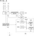
- the circuit part 13 includes an oscillation circuit part 131, an analog multiplexer (MPX) 132, a capacitance detection circuit part 133, an analog/digital (A/D) conversion part 134, a band pass filter (BPS) part 135, and a control part 136.
- the control part 136 includes a digital signal processor (DSP) 1361, a central processing unit (CPU) 1362, a storage part 1363, and a communication part 1364.
- DSP digital signal processor
- CPU central processing unit
- storage part 1363 storage part 1363
- the communication part 1364 are connected with each other via a bus (BUS) .
- the oscillation circuit part 131 is an oscillation circuit that oscillates a sine wave of a predetermined frequency f.
- the oscillation circuit part 131 outputs the oscillated sine wave signal to the analog multiplexer 132, the A/D conversion part 134, the BPF part 135, and the control part 136.
- the analog multiplexer 132 selects one of the multiple electrostatic capacitance sensor 12 after another at a predetermined timing (in a predetermined cycle T sufficiently larger than the cycle t of the sine wave signal, i.e., T>>t), and outputs the sine wave signal output from the oscillation circuit part 131, to the selected electrostatic capacitance sensor 12.
- the capacitance detection circuit part 133 includes an inductor-capacitor (LC) resonant circuit, for example, outputting a resonance signal in resonance with the sine wave signal output to the electrostatic capacitance sensor 12 currently selected by the analog multiplexer 132.
- the frequency f' of the resonance signal varies depending on the distance from the electrostatic capacitance sensor 12 selected by the analog multiplexer 132 to the user's hand or fingertips or on a push-in force (contact area) applied by the user's hand or fingertips to the electrostatic capacitance sensor 12.
- the A/D conversion part 134 converts, to a digital signal, the signal of the frequency f' output from the capacitance detection circuit part 133, and outputs the digital signal resulting from the conversion.
- the BPF part 135 is a digital band-pass filter. From among the digital signals (signals of the frequency f') output from the A/D conversion part 134, the BPF part 135 extracts signals of a frequency component near a predetermined frequency f0.
- the DSP 1361 of the control part 136 performs predetermined digital signal processing on the signal output from the BPF part 135, and outputs the processed signal to the CPU 1362.
- the CPU 1362 operates in accordance with programs stored in the storage part 1363, and determines differences between the signal output from the DSP 1361 and the signal of the frequency f output from the oscillation circuit part 131. On the basis of the detected differences, the CPU 1362 obtains information regarding the electrostatic capacitance sensor 12 currently selected by the analog multiplexer 132, regarding the distance from the selected sensor to the user's hand or fingertip, or regarding a pressing force applied by the user's hand or fingertips to the electrostatic capacitance sensor 12 before outputting the acquired information (referred to as the proximity contact information).
- the storage part 1363 holds the programs to be executed by the CPU 1362.
- the programs may be provided and recorded on non-transitory computer-readable storage media and may be copied into the storage part 1363.
- the storage part 1363 also serves as a work memory for the CPU 1362.
- the communication part 1364 may be a wireless communication interface such as a wireless local area network (LAN) interface or Bluetooth (registered trademark). In accordance with instructions input from the CPU 1362, the communication part 1364 outputs information to the information processing apparatus 20. The communication part 1364 also outputs the information received from the information processing apparatus 20 to the CPU 1362.
- LAN wireless local area network
- Bluetooth registered trademark
- the CPU 1362 of the controller apparatus 10 detects the electrostatic capacitance of each of the electrostatic capacitance sensors 12 selected successively by the analog multiplexer 132 and, on the basis of the detected electrostatic capacitance, outputs, to the information processing apparatus 20, the distance from the sensor to the user's hand or fingertip or the proximity contact information regarding the pressing force applied by the user's hand or fingertips to the electrostatic capacitance sensor 12.
- the CPU 1362 of the controller apparatus 10 is initialized (S11) on startup (at power-on).
- the CPU 1362 detects changes in the electrostatic capacitance of each electrostatic capacitance sensor 12 disposed on or in the vicinity of the surface of the controller main body 11 (S12).
- the CPU 1362 determines whether or not there is any change in electrostatic capacitance exceeding a predetermined threshold value (S13).
- the CPU 1362 stores information identifying the electrostatic capacitance sensor 12 (i.e., information identifying the disposed location) in association with a value indicative of the magnitude of the detected change (S14). The CPU 1362 then returns to step S12 to continue processing the next electrostatic capacitance sensor 12.
- step S13 If, in step S13, the change in electrostatic capacitance detected in step S12 is not found to exceed the predetermined threshold value (S13: No), the CPU 1362 returns to step S12 to continue processing the next electrostatic capacitance sensor 12.
- the CPU 1362 repeatedly executes steps S12 through S14 on each electrostatic capacitance sensor 12. Upon completing the processing of all electrostatic capacitance sensors 12, the CPU 1362 outputs to the information processing apparatus 20 (S15) the information identifying the electrostatic capacitance sensor 12 of which the electrostatic capacitance has changed beyond the predetermined threshold value (information identifying the disposed location) and the information giving the value indicative of the magnitude of the detected change (proximity contact information).
- the CPU 1362 repeatedly executes steps S12 through S14 on each electrostatic capacitance sensor 12 and also performs step S15 until power-off.
- the information processing apparatus 20 may be a home-use game machine, a personal computer, or some other computer devices, for example.
- the information processing apparatus 20 is communicably connected with the controller apparatus 10.
- the information processing apparatus 20 acquires the distance from each electrostatic capacitance sensor 12 disposed on or in the vicinity of the controller main body 11 of the controller apparatus 10 to the user's hand or fingertip, or the proximity contact information regarding the pressing force applied by the user's hand or fingertips to each electrostatic capacitance sensor 12, the distance and the proximity contact information being received from the controller apparatus 10.
- the information processing apparatus 20 estimates the deformation of the controller main body 11. For example, as depicted conceptually in Subfigure (a) of FIG. 5 , it is assumed that the electrostatic capacitance sensors 12a, 12b, 12c, and 12d are disposed at intervals of 90 degrees on a virtual great circle C on the surface of the controller main body 11 that substantially forms a sphere.
- the controller apparatus 10 outputs, for example, the proximity contact information such as the following:
- the information processing apparatus 20 Upon receipt of the proximity contact information, the information processing apparatus 20 estimates that there is no change in the electrostatic capacitance of each of the electrostatic capacitance sensors 12b and 12d not identified by information included in the proximity contact information and that the user's pressing pressure at these locations is zero.
- the information processing apparatus 20 also estimates the user's pressing force F at the locations where the electrostatic capacitance sensors 12 identified by information included in the proximity contact information are disposed, on the basis of the values of the corresponding changes in electrostatic capacitance.
- Well-known methods can be adopted to estimate the pressing force based on the changes in electrostatic capacitance.
- the information processing apparatus 20 thus estimates the user's pressing force F at the location where each electrostatic capacitance sensor 12 of the controller apparatus 10 is disposed in a manner such as the following:
- the information processing apparatus 20 estimates the deformation of the controller main body 11 by use of such pieces of the estimated information. Specifically, in the above example, the information processing apparatus 20 estimates that the electrostatic capacitance sensors 12a and 12c of the controller main body 11 are pressed from both sides so that the controller main body 11 is deformed into a flat shape.
- the above estimation is only an example.
- the information processing apparatus 20 is only required to estimate the deformation of the controller apparatus 10 on the basis of the proximity contact information obtained therefrom and according to experimentally and previously obtained relations between proximity contact information and the deformation of the controller apparatus 10.
- a sensor fit for the case where the main body of the controller apparatus is made deformable.
- the electrode 121 and the lead part 122 of the sensor are disposed in a manner avoiding the wiring of other sensors, which prevents interference between the wiring parts in terms of electrostatic capacitance.
- the electrostatic capacitance sensor 12 of this embodiment is not limited to the configuration in which the electrode 121 and the lead part 122 are disposed on the base part 120 and the lead part 122 is connected with the wiring part 123, as depicted in FIG. 2 .
- the electrode 121 and the lead part 122 may be disposed on the base part 120, the lead part 122 being connected with the wiring part 123, the lead part 122 being further covered at least partially by a covering body 125.
- the covering body 125 is made by use of an elastic insulating material (e.g., insulating organic silicon compound) as with the base part 120.
- the covering body 125 is formed as a thin film-like member as in the case of the base part 120.
- the electrode 121 is formed of an elastic conductive material such as a conductive ink material.
- the lead part 122 also has the end 122a electrically connected to the electrode 121 and is formed of an elastic conductive material in a line shape having a predetermined width on the base part 120.
- the electrostatic capacitance sensor 12 is constituted by the base part 120 as a base layer formed of an elastic insulating material starting from near the inside of the controller main body 11, by the electrode 121 and lead part 122 each formed of an elastic insulating material, and by the covering body 125 as a covering layer at least partially covering the lead part 122, all stacked in this order.
- the covering body 125 may partially expose (not cover) the end of the lead part 122 on the side of the electrode 121 while covering the end of the lead part 122 on the side of the wiring part 123.
- the Young's modulus of the covering body 125 serving as the covering layer be approximately equivalent to that of the base part 120 (i.e., the covering body 125 and the base part 120 should preferably have an approximately equivalent level of elasticity).
- the value of the change in electrostatic capacitance upon contact with the electrode 121 is made different from the value of the change in electrostatic capacitance upon contact with the lead part 122, which improves the accuracy of detection.
- the lead parts 122 of other electrostatic capacitance sensors 12 overlap with each other, the lead parts 122 do not come into electrical contact with one another.
- the electrostatic capacitance sensors 12 do not interfere with each other in terms of electrostatic capacitance, which enhances the degree of freedom in disposing the electrostatic capacitance sensors 12.
Landscapes
- Engineering & Computer Science (AREA)
- General Engineering & Computer Science (AREA)
- Theoretical Computer Science (AREA)
- Multimedia (AREA)
- Human Computer Interaction (AREA)
- Physics & Mathematics (AREA)
- General Physics & Mathematics (AREA)
- Input From Keyboards Or The Like (AREA)
- Measurement Of Length, Angles, Or The Like Using Electric Or Magnetic Means (AREA)
Abstract
Description
- The present invention relates to a sensor and a controller apparatus equipped with the sensor.
- Heretofore, controllers for use with video games have been formed of plastics and like materials that are relatively resistant to elastic deformation.
- Meanwhile, recent years have witnessed an increasing use of techniques for vibration and kinesthetic sense presentation intended to enhance users' gaming experiences.
- Under the above circumstances, proposals have been made to fabricate a controller main body using deformable materials to provide a controller apparatus capable of enhancing haptic experiences.
- However, attempts to arrange electrostatic capacitance sensors designed to detect, for example, physical contact of the user with the surface of the controller main body formed of the deformable materials have met difficulty in causing free deformation of the controller main body because of the electrodes of existing electrostatic capacitance sensors not being deformable. This has led to the problem of the users losing the sense of unity with the controller in terms of touch feel.
- The present invention has been made in view of the above circumstances and provides, as an object, a controller apparatus equipped with a sensor fit for the case where the main body of the controller apparatus is made deformable.
- In order to solve the above problem, according to one embodiment of the present invention, there is provided a controller apparatus including a controller main body configured to be deformable, and at least one sensor configured to be disposed on or in the vicinity of the surface of the controller main body. The sensor has an electrode formed of an elastic conductive material.
- According to the present invention, there is provided a controller apparatus equipped with a sensor fit for the case where the main body of the controller apparatus is made deformable.
-
- [
FIG. 1 ]
FIG. 1 is a schematic block diagram depicting a configuration and connection example of a controller apparatus according to an embodiment of the present invention. - [
FIG. 2 ]
FIG. 2 is a schematic perspective view of an exemplary electrostatic capacitance sensor disposed in the controller apparatus according to the embodiment of the present invention. - [
FIG. 3 ]
FIG. 3 is a block diagram depicting an exemplary circuit part of the controller apparatus according to the embodiment of the present invention. - [
FIG. 4 ]
FIG. 4 is a flowchart indicating an example of information processing by the controller apparatus according to the embodiment of the present invention. - [
FIG. 5 ]
FIG. 5 depicts explanatory diagrams depicting exemplary states of elastic deformation of the controller apparatus according to the embodiment of the present invention. - [
FIG. 6 ]
FIG. 6 depicts schematic perspective views of another exemplary electrostatic capacitance sensor disposed in the controller apparatus according to the embodiment of the present invention. - A preferred embodiment of the present invention is described below with reference to the accompanying drawings. A
controller apparatus 10 as one embodiment of the present invention is configured to have a controllermain body 11, sensors (e.g.,electrostatic capacitance sensors 12 in this case) disposed on or in the vicinity of the surface of the controllermain body 11, and acircuit part 13, as depicted inFIG. 1 . Thecontroller apparatus 10 is communicably connected with aninformation processing apparatus 20 in a wired or wireless manner. - The controller
main body 11 is formed of deformable materials such as polymer gel materials including silicon-based polymer gel materials and urethane-based gel materials; or elastically deformable materials such as elastomer materials including polystylene-based elastomer, olefin-based elastomer, polyvinyl chloride-based elastomer, polyurethane-based elastomer, polyester-based elastomer, and polyamide-based elastomer. The deformation here is meant to include elastic deformation, bending, sliding, and twisting. - The controller
main body 11 has a predetermined shape such as a sphere or a cuboid when not subjected to an external force. - The controller
main body 11 changes its shape elastically in response to the external force applied thereto by the user with fingertips, for example. At least oneelectrostatic capacitance sensor 12 is disposed on or in the vicinity of the surface of the controllermain body 11. Further, thecircuit part 13 is disposed inside the controllermain body 11. - It is to be noted that the vicinity of the surface in this context means an internal space of the controller
main body 11 relatively close to its surface. Specifically, the vicinity of the surface refers to a range in which the sensors such aselectrostatic capacitance sensors 12 can detect the user's action on the controllermain body 11. Accordingly, the range of the vicinity varies for each sensor and depending on the material of the controllermain body 11. For example, in the case where theelectrostatic capacitance sensors 12 are adopted as the sensors, the vicinity is defined as the range in which user's physical contact with the surface of the controllermain body 11 can be detected by the sensors. - Although the sensors are not limited to the
electrostatic capacitance sensors 12 as in the above example, the electrostatic capacitance sensors will be used in the description below for the purpose of clarification. - Each of the
electrostatic capacitance sensors 12 is configured to have abase part 120, anelectrode 121, alead part 122, and awiring part 123 as depicted inFIG. 2 . Here, thebase part 120 is a thin film-like member formed by use of an elastic insulating material (e.g., an insulating organic silicon compound). Theelectrode 121 and thelead part 122 are formed on thebase part 120. Thebase part 120 may be formed integrally with the controllermain body 11. - The
electrode 121 is formed of an elastic conductive material on thebase part 120. Theelectrode 121 is formed to have a predetermined shape having a predetermined area. For example, a conductive ink material may be used as the conductive material forming theelectrode 121. The predetermined shape of theelectrode 121 in this case may be circular, elliptical, rectangular, coiled, or polygonal, for example. Theelectrode 121 may be ring-like in shape and have an outer periphery of one of the above shapes. - The
lead part 122 has anend 122a electrically connected to theelectrode 121. Thelead part 122 is formed of an elastic conductive material in a line shape having a predetermined width on thebase part 120. As in the case of theelectrode 121, a conductive ink material, for example, may be used as the conductive material with which to form thelead part 122. - One end of the
wiring part 123 is electrically connected to theend 122b opposite to theend 122a connected to theelectrode 121. The other end of thewiring part 123 is connected to thecircuit part 13. Thewiring part 123 is disposed in such a manner as not to come into electrical contact with thewiring part 123 of any otherelectrostatic capacitance sensor 12 disposed on or in the vicinity of the surface of the controllermain body 11. - It is to be noted that the
electrostatic capacitance sensors 12 of this example may be self-capacitance sensors or mutual capacitance sensors. It is preferred here that the Young's modulus of thebase part 120 be less than that of the controller main body 11 (i.e., thebase part 120 should preferably be more elastic than the controller main body 11). It is also preferred that the Young's moduli of theelectrode 121 and thelead part 122 be less than the Young's modulus of thebase part 120. - The
circuit part 13 is disposed in the central part of the controllermain body 11 of the controller apparatus 10 (at a location as far from the surface as possible). As depicted inFIG. 3 , for example, thecircuit part 13 includes anoscillation circuit part 131, an analog multiplexer (MPX) 132, a capacitancedetection circuit part 133, an analog/digital (A/D)conversion part 134, a band pass filter (BPS)part 135, and acontrol part 136. Thecontrol part 136 includes a digital signal processor (DSP) 1361, a central processing unit (CPU) 1362, astorage part 1363, and acommunication part 1364. The DSP 1361, theCPU 1362, thestorage part 1363, and thecommunication part 1364 are connected with each other via a bus (BUS) . - The
oscillation circuit part 131 is an oscillation circuit that oscillates a sine wave of a predetermined frequency f. Theoscillation circuit part 131 outputs the oscillated sine wave signal to theanalog multiplexer 132, the A/D conversion part 134, theBPF part 135, and thecontrol part 136. - When multiple
electrostatic capacitance sensors 12 are disposed on or in the vicinity of the surface of the controllermain body 11, theanalog multiplexer 132 selects one of the multipleelectrostatic capacitance sensor 12 after another at a predetermined timing (in a predetermined cycle T sufficiently larger than the cycle t of the sine wave signal, i.e., T>>t), and outputs the sine wave signal output from theoscillation circuit part 131, to the selectedelectrostatic capacitance sensor 12. - The capacitance
detection circuit part 133 includes an inductor-capacitor (LC) resonant circuit, for example, outputting a resonance signal in resonance with the sine wave signal output to theelectrostatic capacitance sensor 12 currently selected by theanalog multiplexer 132. The frequency f' of the resonance signal varies depending on the distance from theelectrostatic capacitance sensor 12 selected by theanalog multiplexer 132 to the user's hand or fingertips or on a push-in force (contact area) applied by the user's hand or fingertips to theelectrostatic capacitance sensor 12. - The A/
D conversion part 134 converts, to a digital signal, the signal of the frequency f' output from the capacitancedetection circuit part 133, and outputs the digital signal resulting from the conversion. TheBPF part 135 is a digital band-pass filter. From among the digital signals (signals of the frequency f') output from the A/D conversion part 134, theBPF part 135 extracts signals of a frequency component near a predetermined frequency f0. - The
DSP 1361 of thecontrol part 136 performs predetermined digital signal processing on the signal output from theBPF part 135, and outputs the processed signal to theCPU 1362. TheCPU 1362 operates in accordance with programs stored in thestorage part 1363, and determines differences between the signal output from theDSP 1361 and the signal of the frequency f output from theoscillation circuit part 131. On the basis of the detected differences, theCPU 1362 obtains information regarding theelectrostatic capacitance sensor 12 currently selected by theanalog multiplexer 132, regarding the distance from the selected sensor to the user's hand or fingertip, or regarding a pressing force applied by the user's hand or fingertips to theelectrostatic capacitance sensor 12 before outputting the acquired information (referred to as the proximity contact information). - The
storage part 1363 holds the programs to be executed by theCPU 1362. The programs may be provided and recorded on non-transitory computer-readable storage media and may be copied into thestorage part 1363. Thestorage part 1363 also serves as a work memory for theCPU 1362. - The
communication part 1364 may be a wireless communication interface such as a wireless local area network (LAN) interface or Bluetooth (registered trademark). In accordance with instructions input from theCPU 1362, thecommunication part 1364 outputs information to theinformation processing apparatus 20. Thecommunication part 1364 also outputs the information received from theinformation processing apparatus 20 to theCPU 1362. - In this embodiment, the
CPU 1362 of thecontroller apparatus 10 detects the electrostatic capacitance of each of theelectrostatic capacitance sensors 12 selected successively by theanalog multiplexer 132 and, on the basis of the detected electrostatic capacitance, outputs, to theinformation processing apparatus 20, the distance from the sensor to the user's hand or fingertip or the proximity contact information regarding the pressing force applied by the user's hand or fingertips to theelectrostatic capacitance sensor 12. - Specifically, as depicted in
FIG. 4 , theCPU 1362 of thecontroller apparatus 10 is initialized (S11) on startup (at power-on). TheCPU 1362 then detects changes in the electrostatic capacitance of eachelectrostatic capacitance sensor 12 disposed on or in the vicinity of the surface of the controller main body 11 (S12). TheCPU 1362 determines whether or not there is any change in electrostatic capacitance exceeding a predetermined threshold value (S13). - If the change in electrostatic capacitance is found here to exceed the predetermined threshold value (S13: Yes), the
CPU 1362 stores information identifying the electrostatic capacitance sensor 12 (i.e., information identifying the disposed location) in association with a value indicative of the magnitude of the detected change (S14). TheCPU 1362 then returns to step S12 to continue processing the nextelectrostatic capacitance sensor 12. - If, in step S13, the change in electrostatic capacitance detected in step S12 is not found to exceed the predetermined threshold value (S13: No), the
CPU 1362 returns to step S12 to continue processing the nextelectrostatic capacitance sensor 12. - The
CPU 1362 repeatedly executes steps S12 through S14 on eachelectrostatic capacitance sensor 12. Upon completing the processing of allelectrostatic capacitance sensors 12, theCPU 1362 outputs to the information processing apparatus 20 (S15) the information identifying theelectrostatic capacitance sensor 12 of which the electrostatic capacitance has changed beyond the predetermined threshold value (information identifying the disposed location) and the information giving the value indicative of the magnitude of the detected change (proximity contact information). - Thereafter, the
CPU 1362 repeatedly executes steps S12 through S14 on eachelectrostatic capacitance sensor 12 and also performs step S15 until power-off. - The
information processing apparatus 20 may be a home-use game machine, a personal computer, or some other computer devices, for example. Theinformation processing apparatus 20 is communicably connected with thecontroller apparatus 10. In this embodiment, theinformation processing apparatus 20 acquires the distance from eachelectrostatic capacitance sensor 12 disposed on or in the vicinity of the controllermain body 11 of thecontroller apparatus 10 to the user's hand or fingertip, or the proximity contact information regarding the pressing force applied by the user's hand or fingertips to eachelectrostatic capacitance sensor 12, the distance and the proximity contact information being received from thecontroller apparatus 10. - On the basis of the proximity contact information regarding each
electrostatic capacitance sensor 12, theinformation processing apparatus 20 estimates the deformation of the controllermain body 11. For example, as depicted conceptually in Subfigure (a) ofFIG. 5 , it is assumed that theelectrostatic capacitance sensors main body 11 that substantially forms a sphere. - Here, if the user pushes the
electrostatic capacitance sensors 12c 12d from both sides to deform the controllermain body 11 into a flat shape as depicted in Subfigure (b) ofFIG. 5 , a pressing force F is applied by the user's fingertips to theelectrostatic capacitance sensors electrostatic capacitance sensors controller apparatus 10 outputs, for example, the proximity contact information such as the following: -
electrostatic capacitance sensor 12a: C1 -
electrostatic capacitance sensor 12c: C2 - where, C1 and C2 represent the changes in the electrostatic capacitance of each of the
electrostatic capacitance sensors - Upon receipt of the proximity contact information, the
information processing apparatus 20 estimates that there is no change in the electrostatic capacitance of each of theelectrostatic capacitance sensors - The
information processing apparatus 20 also estimates the user's pressing force F at the locations where theelectrostatic capacitance sensors 12 identified by information included in the proximity contact information are disposed, on the basis of the values of the corresponding changes in electrostatic capacitance. Well-known methods can be adopted to estimate the pressing force based on the changes in electrostatic capacitance. - The
information processing apparatus 20 thus estimates the user's pressing force F at the location where eachelectrostatic capacitance sensor 12 of thecontroller apparatus 10 is disposed in a manner such as the following: -
electrostatic capacitance sensor 12a: F -
electrostatic capacitance sensor 12b: 0 -
electrostatic capacitance sensor 12c: F -
electrostatic capacitance sensor 12d: 0 - The
information processing apparatus 20 estimates the deformation of the controllermain body 11 by use of such pieces of the estimated information. Specifically, in the above example, theinformation processing apparatus 20 estimates that theelectrostatic capacitance sensors main body 11 are pressed from both sides so that the controllermain body 11 is deformed into a flat shape. - The above estimation is only an example. The
information processing apparatus 20 is only required to estimate the deformation of thecontroller apparatus 10 on the basis of the proximity contact information obtained therefrom and according to experimentally and previously obtained relations between proximity contact information and the deformation of thecontroller apparatus 10. - According to the example of the embodiment discussed above, there is provided a sensor fit for the case where the main body of the controller apparatus is made deformable. The
electrode 121 and thelead part 122 of the sensor are disposed in a manner avoiding the wiring of other sensors, which prevents interference between the wiring parts in terms of electrostatic capacitance. - The
electrostatic capacitance sensor 12 of this embodiment is not limited to the configuration in which theelectrode 121 and thelead part 122 are disposed on thebase part 120 and thelead part 122 is connected with thewiring part 123, as depicted inFIG. 2 . - In another example, as depicted in the perspective view ((a) and the cross-sectional view (b)) of
FIG. 6 , theelectrode 121 and thelead part 122 may be disposed on thebase part 120, thelead part 122 being connected with thewiring part 123, thelead part 122 being further covered at least partially by a coveringbody 125. - The covering
body 125 is made by use of an elastic insulating material (e.g., insulating organic silicon compound) as with thebase part 120. The coveringbody 125 is formed as a thin film-like member as in the case of thebase part 120. - In this example, too, the
electrode 121 is formed of an elastic conductive material such as a conductive ink material. Thelead part 122 also has theend 122a electrically connected to theelectrode 121 and is formed of an elastic conductive material in a line shape having a predetermined width on thebase part 120. - In this example, that is, the
electrostatic capacitance sensor 12 is constituted by thebase part 120 as a base layer formed of an elastic insulating material starting from near the inside of the controllermain body 11, by theelectrode 121 andlead part 122 each formed of an elastic insulating material, and by the coveringbody 125 as a covering layer at least partially covering thelead part 122, all stacked in this order. For example, the coveringbody 125 may partially expose (not cover) the end of thelead part 122 on the side of theelectrode 121 while covering the end of thelead part 122 on the side of thewiring part 123. - Here, it is preferred that the Young's modulus of the covering
body 125 serving as the covering layer be approximately equivalent to that of the base part 120 (i.e., the coveringbody 125 and thebase part 120 should preferably have an approximately equivalent level of elasticity). - When the
electrostatic capacitance sensors 12 of this example are used on or in the proximity of the surface of the controllermain body 11, the value of the change in electrostatic capacitance upon contact with theelectrode 121 is made different from the value of the change in electrostatic capacitance upon contact with thelead part 122, which improves the accuracy of detection. In addition, even if thelead parts 122 of otherelectrostatic capacitance sensors 12 overlap with each other, thelead parts 122 do not come into electrical contact with one another. Thus disposed, theelectrostatic capacitance sensors 12 do not interfere with each other in terms of electrostatic capacitance, which enhances the degree of freedom in disposing theelectrostatic capacitance sensors 12. -
- 10: Controller apparatus
- 11: Controller main body
- 12: Electrostatic capacitance sensor
- 13: Circuit part
- 20: Information processing apparatus
- 120: Base part
- 121: Electrode
- 122: Lead part
- 123: Wiring part
- 125: Covering body
- 131: Oscillation circuit part
- 132: Analog multiplexer
- 133: Capacitance detection circuit part
- 134: A/D conversion part
- 135: BPF part
- 136: Control part
- 1361: DSP
- 1362: CPU
- 1363: Storage part
- 1364: Communication part
Claims (6)
- A controller apparatus comprising:a controller main body configured to be deformable; andat least one sensor configured to be disposed on or in a vicinity of a surface of the controller main body, whereinthe sensor has an electrode formed of an elastic conductive material.
- The controller apparatus according to claim 1, whereinthe sensor has the electrode formed of the elastic conductive material and a lead part electrically connected to the electrode and formed of an elastic conductive material, andthe lead part is covered at least partially by an elastic insulating material.
- The controller apparatus according to claim 1 or 2, whereinthe sensor includes a base layer formed of an elastic insulating material starting from near an inside of the controller main body, and an electrode layer having the electrode formed of the elastic conductive material, andthe electrode layer has a lead part electrically connected to the electrode and formed of an elastic conductive material, the lead part being covered at least partially by a covering layer formed of an elastic insulating material.
- The controller apparatus according to any one of claims 1 to 3, wherein the sensor is an electrostatic capacitance sensor.
- The controller apparatus according to any one of claims 1 to 4, wherein the controller main body is elastically deformable.
- A sensor disposed on or in a vicinity of a surface of a deformable controller main body, the sensor comprising:
an electrode formed of an elastic conductive material.
Applications Claiming Priority (1)
| Application Number | Priority Date | Filing Date | Title |
|---|---|---|---|
| PCT/JP2022/014190 WO2023181312A1 (en) | 2022-03-24 | 2022-03-24 | Controller device and sensor |
Publications (2)
| Publication Number | Publication Date |
|---|---|
| EP4502773A1 true EP4502773A1 (en) | 2025-02-05 |
| EP4502773A4 EP4502773A4 (en) | 2026-01-28 |
Family
ID=88100785
Family Applications (1)
| Application Number | Title | Priority Date | Filing Date |
|---|---|---|---|
| EP22933452.9A Pending EP4502773A4 (en) | 2022-03-24 | 2022-03-24 | Controller device and sensor |
Country Status (4)
| Country | Link |
|---|---|
| US (1) | US20250190079A1 (en) |
| EP (1) | EP4502773A4 (en) |
| JP (1) | JPWO2023181312A1 (en) |
| WO (1) | WO2023181312A1 (en) |
Family Cites Families (13)
| Publication number | Priority date | Publication date | Assignee | Title |
|---|---|---|---|---|
| JP5441299B2 (en) * | 2006-11-01 | 2014-03-12 | 株式会社ソニー・コンピュータエンタテインメント | Controller device |
| KR101661526B1 (en) * | 2012-04-08 | 2016-10-04 | 삼성전자주식회사 | Flexible display apparatus and user interface providing method thereof |
| US20150277617A1 (en) * | 2014-03-28 | 2015-10-01 | Paul Gwin | Flexible sensor |
| GB201511042D0 (en) * | 2015-06-23 | 2015-08-05 | Royal College Of Art And Kong Ming | Sensor device and method |
| US10427397B2 (en) * | 2016-01-27 | 2019-10-01 | Palo Alto Research Center Incorporated | Structural designs for stretchable, conformal electrical interconnects |
| EP3216499A1 (en) * | 2016-03-08 | 2017-09-13 | iibip ApS | Responsive training device |
| KR102632730B1 (en) * | 2016-03-23 | 2024-02-06 | 삼성디스플레이 주식회사 | Electronic device |
| CN109074153A (en) * | 2016-03-29 | 2018-12-21 | 斋藤创造研究所株式会社 | A kind of input unit and image display system |
| KR102347989B1 (en) * | 2017-04-14 | 2022-01-10 | 삼성디스플레이 주식회사 | Electronic device |
| GB2573752B (en) * | 2018-05-11 | 2022-12-07 | Tangi0 Ltd | Sensor device and method |
| US10838486B2 (en) * | 2019-02-28 | 2020-11-17 | Microsoft Technology Licensing, Llc | Virtual reality controller |
| US12274934B2 (en) * | 2020-03-25 | 2025-04-15 | Sony Interactive Entertainment Inc. | Controller |
| US20240269465A1 (en) * | 2021-06-22 | 2024-08-15 | Niche Biomedical, Inc. | Multi-electrode pad for transcutaneous stimulation |
-
2022
- 2022-03-24 US US18/843,521 patent/US20250190079A1/en active Pending
- 2022-03-24 WO PCT/JP2022/014190 patent/WO2023181312A1/en not_active Ceased
- 2022-03-24 JP JP2024509620A patent/JPWO2023181312A1/ja active Pending
- 2022-03-24 EP EP22933452.9A patent/EP4502773A4/en active Pending
Also Published As
| Publication number | Publication date |
|---|---|
| JPWO2023181312A1 (en) | 2023-09-28 |
| EP4502773A4 (en) | 2026-01-28 |
| US20250190079A1 (en) | 2025-06-12 |
| WO2023181312A1 (en) | 2023-09-28 |
Similar Documents
| Publication | Publication Date | Title |
|---|---|---|
| CN114205706B (en) | Force-activated headphones | |
| US10871830B2 (en) | Proximity detection for an input mechanism of an electronic device | |
| US11537230B2 (en) | Electronic device for identifying gesture performed by stylus pen and method for operating the same | |
| CN108700970B (en) | Input device with force sensor | |
| CN110138372B (en) | Touch button assemblies, control circuits and electronic equipment | |
| US20190204929A1 (en) | Devices and methods for dynamic association of user input with mobile device actions | |
| CN113918027B (en) | Gesture finger stall control method, gesture finger stall, system, equipment and storage medium | |
| JP2013222283A (en) | Electronic device, and method and program for controlling the same | |
| EP3677924A1 (en) | Method and electronic device for correcting measurement value of sensor | |
| CN211268917U (en) | Intelligent ring with rotation control function | |
| US20250190079A1 (en) | Controller apparatus and sensor | |
| US20100164759A1 (en) | Input Arrangement | |
| CN107050853A (en) | A kind of game paddle and its touch control detecting method, a kind of game station | |
| CN116166135A (en) | Intelligent ring, interaction method based on intelligent ring, intelligent glasses assembly and computer readable storage medium | |
| CN112449297B (en) | A kind of detection method of earphone wearing state | |
| JP2011150964A (en) | Switch | |
| US20240314480A1 (en) | Method for sensing wearing of electronic device, and electronic device | |
| US10534435B2 (en) | Handheld interface device having a plurality of electrostatic friction (ESF) electrodes | |
| US20250303312A1 (en) | Interaction apparatus | |
| JPWO2006049275A1 (en) | Coordinate indicating system and method | |
| KR20190089201A (en) | Method and system for capacitive handle | |
| CN114594896A (en) | Gesture finger stall control method, gesture finger stall, system, equipment and storage medium | |
| KR101545702B1 (en) | A mobile terminal operating based on detection data and a method of operation thereof | |
| CN107995968B (en) | Wire-controlled device and wire-controlled method of user terminal | |
| KR20220149355A (en) | Electronic device including sensor device and method for thereof |
Legal Events
| Date | Code | Title | Description |
|---|---|---|---|
| STAA | Information on the status of an ep patent application or granted ep patent |
Free format text: STATUS: THE INTERNATIONAL PUBLICATION HAS BEEN MADE |
|
| PUAI | Public reference made under article 153(3) epc to a published international application that has entered the european phase |
Free format text: ORIGINAL CODE: 0009012 |
|
| STAA | Information on the status of an ep patent application or granted ep patent |
Free format text: STATUS: REQUEST FOR EXAMINATION WAS MADE |
|
| 17P | Request for examination filed |
Effective date: 20240907 |
|
| AK | Designated contracting states |
Kind code of ref document: A1 Designated state(s): AL AT BE BG CH CY CZ DE DK EE ES FI FR GB GR HR HU IE IS IT LI LT LU LV MC MK MT NL NO PL PT RO RS SE SI SK SM TR |
|
| DAV | Request for validation of the european patent (deleted) | ||
| DAX | Request for extension of the european patent (deleted) | ||
| A4 | Supplementary search report drawn up and despatched |
Effective date: 20260107 |
|
| RIC1 | Information provided on ipc code assigned before grant |
Ipc: G06F 3/041 20060101AFI20251222BHEP Ipc: A63F 13/24 20140101ALI20251222BHEP Ipc: A63F 13/285 20140101ALI20251222BHEP |