EP4501661A1 - Anti-counterfeiting object and methods for manufacture and authenticate it - Google Patents
Anti-counterfeiting object and methods for manufacture and authenticate it Download PDFInfo
- Publication number
- EP4501661A1 EP4501661A1 EP23306327.0A EP23306327A EP4501661A1 EP 4501661 A1 EP4501661 A1 EP 4501661A1 EP 23306327 A EP23306327 A EP 23306327A EP 4501661 A1 EP4501661 A1 EP 4501661A1
- Authority
- EP
- European Patent Office
- Prior art keywords
- substance
- terminals
- phase
- xrd
- conductor
- Prior art date
- Legal status (The legal status is an assumption and is not a legal conclusion. Google has not performed a legal analysis and makes no representation as to the accuracy of the status listed.)
- Withdrawn
Links
Images


Classifications
-
- B—PERFORMING OPERATIONS; TRANSPORTING
- B42—BOOKBINDING; ALBUMS; FILES; SPECIAL PRINTED MATTER
- B42D—BOOKS; BOOK COVERS; LOOSE LEAVES; PRINTED MATTER CHARACTERISED BY IDENTIFICATION OR SECURITY FEATURES; PRINTED MATTER OF SPECIAL FORMAT OR STYLE NOT OTHERWISE PROVIDED FOR; DEVICES FOR USE THEREWITH AND NOT OTHERWISE PROVIDED FOR; MOVABLE-STRIP WRITING OR READING APPARATUS
- B42D25/00—Information-bearing cards or sheet-like structures characterised by identification or security features; Manufacture thereof
- B42D25/30—Identification or security features, e.g. for preventing forgery
- B42D25/305—Associated digital information
-
- B—PERFORMING OPERATIONS; TRANSPORTING
- B42—BOOKBINDING; ALBUMS; FILES; SPECIAL PRINTED MATTER
- B42D—BOOKS; BOOK COVERS; LOOSE LEAVES; PRINTED MATTER CHARACTERISED BY IDENTIFICATION OR SECURITY FEATURES; PRINTED MATTER OF SPECIAL FORMAT OR STYLE NOT OTHERWISE PROVIDED FOR; DEVICES FOR USE THEREWITH AND NOT OTHERWISE PROVIDED FOR; MOVABLE-STRIP WRITING OR READING APPARATUS
- B42D25/00—Information-bearing cards or sheet-like structures characterised by identification or security features; Manufacture thereof
- B42D25/30—Identification or security features, e.g. for preventing forgery
- B42D25/36—Identification or security features, e.g. for preventing forgery comprising special materials
-
- B—PERFORMING OPERATIONS; TRANSPORTING
- B42—BOOKBINDING; ALBUMS; FILES; SPECIAL PRINTED MATTER
- B42D—BOOKS; BOOK COVERS; LOOSE LEAVES; PRINTED MATTER CHARACTERISED BY IDENTIFICATION OR SECURITY FEATURES; PRINTED MATTER OF SPECIAL FORMAT OR STYLE NOT OTHERWISE PROVIDED FOR; DEVICES FOR USE THEREWITH AND NOT OTHERWISE PROVIDED FOR; MOVABLE-STRIP WRITING OR READING APPARATUS
- B42D25/00—Information-bearing cards or sheet-like structures characterised by identification or security features; Manufacture thereof
- B42D25/30—Identification or security features, e.g. for preventing forgery
- B42D25/36—Identification or security features, e.g. for preventing forgery comprising special materials
- B42D25/373—Metallic materials
-
- G—PHYSICS
- G07—CHECKING-DEVICES
- G07D—HANDLING OF COINS OR VALUABLE PAPERS, e.g. TESTING, SORTING BY DENOMINATIONS, COUNTING, DISPENSING, CHANGING OR DEPOSITING
- G07D7/00—Testing specially adapted to determine the identity or genuineness of valuable papers or for segregating those which are unacceptable, e.g. banknotes that are alien to a currency
- G07D7/004—Testing specially adapted to determine the identity or genuineness of valuable papers or for segregating those which are unacceptable, e.g. banknotes that are alien to a currency using digital security elements, e.g. information coded on a magnetic thread or strip
- G07D7/0043—Testing specially adapted to determine the identity or genuineness of valuable papers or for segregating those which are unacceptable, e.g. banknotes that are alien to a currency using digital security elements, e.g. information coded on a magnetic thread or strip using barcodes
-
- G—PHYSICS
- G07—CHECKING-DEVICES
- G07D—HANDLING OF COINS OR VALUABLE PAPERS, e.g. TESTING, SORTING BY DENOMINATIONS, COUNTING, DISPENSING, CHANGING OR DEPOSITING
- G07D7/00—Testing specially adapted to determine the identity or genuineness of valuable papers or for segregating those which are unacceptable, e.g. banknotes that are alien to a currency
- G07D7/02—Testing electrical properties of the materials thereof
- G07D7/023—Measuring conductivity by direct contact
-
- G—PHYSICS
- G07—CHECKING-DEVICES
- G07D—HANDLING OF COINS OR VALUABLE PAPERS, e.g. TESTING, SORTING BY DENOMINATIONS, COUNTING, DISPENSING, CHANGING OR DEPOSITING
- G07D7/00—Testing specially adapted to determine the identity or genuineness of valuable papers or for segregating those which are unacceptable, e.g. banknotes that are alien to a currency
- G07D7/06—Testing specially adapted to determine the identity or genuineness of valuable papers or for segregating those which are unacceptable, e.g. banknotes that are alien to a currency using wave or particle radiation
Definitions
- the invention purpose is to provide an identification substance to build an anti-counterfeiting object
- Counterfeiting is a longstanding problem that is growing in scope and magnitude. Counterfeiting is a concern to businesses because of the impact that it has on sales, brand value and a firm's reputation, as well as on the ability to benefit from technical innovations. Consumers are of course also victims of counterfeiting, being defrauded of the genuine product they have paid for and, with regard to e.g. goods such as mechanical parts or drugs, running significant health and safety risks. At State level, counterfeiting is a concern for governments because of the threat it poses to the welfare and health of consumers, the negative impact it can have on innovation, and the substantial resources channeled to criminal networks, organized crime and other groups that disrupt and corrupt society.
- One particular challenge of anti-counterfeiting measures is the difficulty to prevent copying of the RFID device, taggant, hologram or other fingerprint.
- US 2007/0121181 discloses a method of labeling and identifying an item based on X-ray diffraction (XRD) analysis.
- the method employs an optical identification element formed by powdered crystal materials in a binder to provide a composite X-ray diffraction pattern when illuminated by an X-ray beam.
- the composite X-ray diffraction pattern is indicative of the item.
- the method further relies on the use of a composite X-ray diffraction pattern "encoded" by the selection and omission of one or more of the four different crystalline materials.
- Document EP 3428628 A1 uses also a method of marking and identifying an item based on X-ray diffraction (XRD) analysis. For that, a identification substance including amorphous phase, crystalline phase and complex metallic phase is manufactured to give a specific XRD signature to the item by adjusting geometry and composition of said identification substance. It has not be demonstrated that such an item could be reproduced by retro engineering. Thus, items can be authenticated with a high level of security.
- XRD X-ray diffraction
- the method has the disadvantage of requiring unusual analysis resources.
- the invention has for object a method of building an anti-counterfeiting object, said method comprising the steps of:
- incorporating a conductor allows to confer a specific characteristic to the object, i. e. that there is an electrical conduction between the two terminals, or that a resistance can be measured between them.
- the presence or the lack of the electrical continuity can be checked very easily with an electrical tester.
- the value of the resistance can be easily accessed with a simple ohmmeter.
- a plurality of conductors will be used in the object in the goal of multiplying possible combination of continuity or resistance.
- the anti-counterfeiting object can be the product itself, a taggant incorporated in the product or in the packaging of the product.
- XRD signature is used herein to designate at least a part of the XRD diffraction pattern measured for a reference identification substance or a candidate that contains characteristic values of the XRD pattern.
- the XRD signature can be stored graphically or as a data set; also, only a part, or some parts, of the XRD pattern may be used for authentication purposes.
- the XRD signature preferably comprises a characteristic set of angles and intensity values representative of the analyzed sample.
- the step of comparing the measured XRD signature to the reference sample thus consists in comparing the correspondence of the respective XRD signatures (graphically or numerically).
- the candidate and reference XRD signatures are considered to match when the angular positions of the peaks and intensities correspond exactly or are within a certain tolerance range.
- the comparison step will mainly involve comparing angular positions of representative/characteristic peaks and/or comparing relative intensities between representative/characteristic peaks.
- the identification substance preferably comprises a known calibration crystal, such as e.g. a silicon. This will allow precise positioning along the x axis (theta) of the diffraction diagram.
- the object can be manufactured by injecting first the identification substance in a first volume, then by injecting the substrate substance around a part of the first volume.
- the identification substance is preferably changed between each object to present changed characteristics as the conductivity.
- the form of the first volume is changed, for example with a modular mold.
- the conductive microparticles or nanoparticles are chosen in group including carbon, graphene and graphite. Such particles are enough conductive without altering the other properties of the substance.
- the present method can be easily implemented with present technologies.
- a variety of materials are available to provide the four required phases.
- X-ray diffraction analysis is a standard technology and any appropriate X-ray diffraction measurement system may be used.
- the sample substance to be analyzed does not need particular preparation.
- the obtained diffraction patterns and corresponding signatures can be stored on any computer readable support.
- an amorphous or semi-crystalline polymer can be used as matrix, to which particles containing the other required phases are added.
- particles containing the other required phases are added.
- powders and finer or coarser particulate material containing one or more crystalline phases, one or more complex metallic phases and conductive particles are selected and added to the polymer matrix according to predetermined amounts, depending on the desired mixture.
- amorphous phase is used in its conventional meaning, generally designating non-periodic 3D structural arrangement, lacking the long-range order that is characteristic of a crystal.
- X-rays will be scattered in many directions leading to only broad peaks characteristic of not well-defined short-range order.
- the amorphous phase is provided by a polymer.
- crystalline phase is used in its classical crystallographic meaning, designating crystal structure, i.e. an ordered arrangement of atoms, ions or molecules, forming symmetric patterns that repeat periodically along the principal directions of the three-dimensional space in matter.
- the term “crystalline phase” thus covers the historic definition of crystals, and does not encompass so-called “quasicrystals” or more generally “complex metallic alloys”, as defined below.
- Crystalline phases have powder XRD patterns characterized by a finite set of sharp and intense diffraction peaks.
- complex metallic alloy designates an alloy that is either a quasi-crystalline phase strictly speaking, or else so-called approximant phases.
- Quasi-crystalline phases in the strict sense are phases presenting forbidden rotational symmetries that are normally incompatible with translational symmetry characteristic of classical crystals: i.e. rotational symmetries of order 5, 8, 10, or 12.
- rotational symmetries of order 5, 8, 10, or 12.
- Approximant phases or approximant compounds are true crystals insofar as their crystallographic structure remains compatible with translational symmetry with short range order similar to that of quasi-crystals, but in an electron diffraction shot they present diffraction patterns of symmetry close to symmetry of order 5, 8, 10, or 12. They are phases characterized by an elementary mesh containing several tens or even several hundreds of atoms, and in which local order presents arrangements of almost icosahedral or decagonal symmetry similar to the related quasi-crystalline phases.
- Complex metallic alloys have powder XRD characterized by a dense set of sharp and intense diffraction peaks, significantly more complex than regular metallic alloys.
- the invention concerns an anti-counterfeiting object comprising at least a substrate substance which is electrically insulating material, at least one conductor included in the substrate substance, characterized in that the at least one conductor is of an identification substance as previously described.
- the XRD signature is a mix of the answer of the substrate substance and the identification substance, according to the respective volume and to the location of the substances inside the object within the analyzed area.
- the object comprises at least two accessible terminals electrically connected together via the at least one conductor.
- the terminals have a surface which is conductive, such that one can establish a circuit including the at least one conductor, in particular to test the conductivity or to measure the resistance.
- Some terminals can be common to more than one conductor.
- a test device comprising connectors and being configured so that each connector is in contact with one of the terminals of the object in a test position, the test device comprising at least one electrical continuity tester between at least two connectors, the tester giving a positive indication when it detects electrical continuity provided by the object between two connectors.
- FIG. 1 An object 1 according to a first embodiment of the invention is shown in Figure 1 .
- This object 1 has a parallelepiped shape with, in particular, an upper face 10 on which four terminals 11, 12, 13, 14 are flush.
- a first conductor 15 connects a first and a second of the terminals 11, 12.
- a second conductor 16 connects the second terminal 12 to a third of the terminals 13.
- a third conductor 17 connects the third to a fourth of the terminals 13, 14.
- the resistance of each of the three conductors 15, 16, 17 can be measured between the terminals 11, 12, 13, 14 which connect the ends of the conductor to be measured, for example between the first and second terminals 11, 12 for the first conductor 15.
- the resistance value is almost always greater than 10 kQ, often greater than 100 kQ, or even greater than 1 MS2.
- the object 1 is manufactured by additive manufacturing using molten wire deposition, known also as fused filament fabrication (FFF).
- FFF fused filament fabrication
- a first layer is deposited on a plate to form the lower face, opposite to the upper face 10. Layers are then formed on top of the previous layer and parallel to it, the stacking of layers thus producing the complete object 1.
- the filament used as the second material i.e. the identification substance used for printing all objects is made for example of 70% mass of polymer containing an amorphous phase (e.g. PLA), 12.5% mass of approximant metallic alloy, 12.5% mass of quasi crystalline alloy and graphene particles at 5% mass.
- Conductive particles size is preferably between 1 and 100 micrometers.
- Such objects are manufactured in batches, and at least one parameter for at least one of the conductors 15, 16, 17 is modified from one object 1 to another so as to modify the resistance value of said conductor.
- the parameters that can be modified are the path of the conductor, the cross-section of the conductor over at least part of the path, the material of the conductor, and a number of passes through the conductor.
- the paths of the three conductors 15', 16', 17' have been modified compared to the example in figure 1 , while the terminals 11', 12', 13', 14' are in the same place.
- the resistance value of each of the three conductors between the terminals is measured after manufacture.
- a record of the three values measured for the object is created in a register.
- the resistance values for each of the object's conductors are measured and compared with the values in the records of the register.
- the object to be authenticated is considered authentic if there is a record for which the three resistance values measured correspond to that of the record.
- the next step is to carry out an XRD analysis of the sample. Whether XRD pattern reveals presence of expected material, by representative set of angles and intensity values or not, allow to act proper authentic substance is used.
- the object may be the product itself, which the consumer buys and wants to be guaranteed by the manufacture. They can take the resistance measurements themselves or with the help of a retailer, and submit them to the manufacturer, who holds the register and can in turn indicate whether the object is an original.
- the object may be incorporated into the product in such a way that it can only be removed by breaking off part of the product or object.
- the object may also be incorporated into a container or packaging of the product.
- FIG. 3 An object 2 according to a second embodiment of the invention is shown in Figure 3 .
- This object 2 is substantially in the form of a pentagonal-shaped plate.
- Five terminals 21, 22, 23, 24, 25 are provided flush with the face seen in Figure 3 , distributed regularly at the vertices of a pentagon inscribed in the contour of the plate.
- the terminals are distributed in a regularly repeated pattern around the center of the pentagon.
- Conductors 26, 27 connect terminals 21, 25 and 22, 25 respectively.
- a control device 3, as shown in Figure 4 is also substantially in the form of a pentagonal-shaped plate.
- Five connectors 31, 32, 33, 34, 35 project from the surface to come into contact with the terminals 21, 22, 23, 24, 25 of the object 2, placing the object 2 and the testing device 3 opposite each other.
- the testing device comprises an electrical continuity tester, connector 35 and the group of connectors 31 and 32. When the connectors are pressed against the terminals, electrical contact is established between connector 31 and terminal 21, between connector 32 and terminal 22, and between connector 35 and terminal 25.
- the tester then gives a positive indication because it detects electrical continuity passing through connector 35, terminal 25, conductor 26, terminal 21 and connector 31.
- the positive indication also comes from the electrical continuity detected passing through connector 35, terminal 25, conductor 27, terminal 22 and connector 32.
- object 4 differs from that of Figure 3 in that it has a conductor between terminals 41, 45 and another between terminals 42, 44.
- the testing device not shown but identical in appearance to that of Figure 4 , comprises a first electrical continuity tester between connector 35 and connector 31, and a second continuity tester between connectors 32 and 34.
- the first tester gives a positive indication because it detects electrical continuity passing through connector 35, terminal 45, conductor 46, terminal 41 and connector 31.
- the second tester also gives a positive indication because it detects electrical continuity passing through connector 32, terminal 42, conductor 47, terminal 44 and connector 34. The test is considered positive when both testers give a positive indication.
- the object differs from that of the second embodiment in that it comprises ten terminals, numbered 0 to 9 in Figure 6 , distributed at the vertices of a regular decagon.
- Conductors connect terminals 1-2, 4-10 and 5-9.
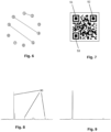
- the object shown in figure 7 , has a QR code printed at its surface.
- the black parts are in the identification substance and the white parts are in the substrate substance, like PLA.
- the object has three terminals 51, 52, 53 included in the QR code, and a first conductor connects first and second terminal 51, 52 and a second conductor connects second and third terminals 52, 53. Conductors are realized with the identification substance and are not visible from the surface, they are included in underlying layers under the QR code.
- the XRD signature is measured as well as the resistances of the first and second conductors, and the measures are stored in the register.
- the resistances between first and second terminals, then second and third terminals, are measured.
- the QR code allows to know which record in the register matches the object.
- the values of resistances are compared to the ones from the register and the object is considered as counterfeiting if there is no conduction or the resistance do not match, to within measurement errors.
- a second test can be conducted, by submitting the object to a XRD analysis.
- the diagram of figure 8 is the result of the XRD analysis of the identification substance used for building authentic object and is registered.
- the diagram of figure 9 is the result of the XRD analysis of a counterfeiting object. In the case of figure 9 , the lack of representative peaks in comparison with the peaks 80 in diagram of figure 8 acts the object tested to be a copy.
- the resistance test is conducted first, and if resistances match, the XRD analyse is also conducted to confirm the authenticity.
- the resistance test is conducted first, and if resistances match, we consider that the object is authentic. If they don't match and we think that the mismatch is because of a breakage of the object, a XRD analysis is conducted and the object is considered authentic if the diagram of the analysis match the diagram of the register.
Landscapes
- Physics & Mathematics (AREA)
- General Physics & Mathematics (AREA)
- Health & Medical Sciences (AREA)
- General Health & Medical Sciences (AREA)
- Toxicology (AREA)
- Engineering & Computer Science (AREA)
- Computer Security & Cryptography (AREA)
- Credit Cards Or The Like (AREA)
Abstract
A method of building an anti-counterfeiting object (1, 1', 2, 3, 4) comprises the steps of:
a) manufacturing an identification substance including at least one amorphous phase, at least one crystalline phase, at least one complex metallic phase and at least one conductive material;
b) selecting at least one substrate substance which is electrically insulating material;
c) associating an amount of said identification substance to the substrate substance to form an object, the identification substance realizing at least one conductor (15, 16, 17, 15', 16', 17', 26, 27, 46, 47) between at least two terminals (11, 12, 13, 14, 21, 22, 23, 24, 25, 41, 45, 51, 52, 53).
a) manufacturing an identification substance including at least one amorphous phase, at least one crystalline phase, at least one complex metallic phase and at least one conductive material;
b) selecting at least one substrate substance which is electrically insulating material;
c) associating an amount of said identification substance to the substrate substance to form an object, the identification substance realizing at least one conductor (15, 16, 17, 15', 16', 17', 26, 27, 46, 47) between at least two terminals (11, 12, 13, 14, 21, 22, 23, 24, 25, 41, 45, 51, 52, 53).
Object build with this method and method of identifying such an object.
Description
- The invention purpose is to provide an identification substance to build an anti-counterfeiting object
- Counterfeiting is a longstanding problem that is growing in scope and magnitude. Counterfeiting is a concern to businesses because of the impact that it has on sales, brand value and a firm's reputation, as well as on the ability to benefit from technical innovations. Consumers are of course also victims of counterfeiting, being defrauded of the genuine product they have paid for and, with regard to e.g. goods such as mechanical parts or drugs, running significant health and safety risks. At State level, counterfeiting is a concern for governments because of the threat it poses to the welfare and health of consumers, the negative impact it can have on innovation, and the substantial resources channeled to criminal networks, organized crime and other groups that disrupt and corrupt society.
- Today, there are a multitude of technologies that can be used in the fight against counterfeit goods. Current anti-counterfeiting technology options comprise a range of overt and covert measures which encompass product authentication and security. The anti-counterfeiting market can be mainly categorized into two segments, namely authentication technologies (the technologies providing overt and covert security features); and Track & Trace Technologies (the technologies facilitating visibility of products throughout the supply chain).
- These technology options include serial numbers, barcodes, datamatrix and RFID for identification, and holograms, biometric solutions, watermarks and taggants for security. These technologies have their own limitations at different levels and are not foolproof.
- One particular challenge of anti-counterfeiting measures is the difficulty to prevent copying of the RFID device, taggant, hologram or other fingerprint.
-
US 2007/0121181 discloses a method of labeling and identifying an item based on X-ray diffraction (XRD) analysis. The method employs an optical identification element formed by powdered crystal materials in a binder to provide a composite X-ray diffraction pattern when illuminated by an X-ray beam. The composite X-ray diffraction pattern is indicative of the item. The method further relies on the use of a composite X-ray diffraction pattern "encoded" by the selection and omission of one or more of the four different crystalline materials. - Document
EP 3428628 A1 uses also a method of marking and identifying an item based on X-ray diffraction (XRD) analysis. For that, a identification substance including amorphous phase, crystalline phase and complex metallic phase is manufactured to give a specific XRD signature to the item by adjusting geometry and composition of said identification substance. It has not be demonstrated that such an item could be reproduced by retro engineering. Thus, items can be authenticated with a high level of security. - Despite these advantages, the method has the disadvantage of requiring unusual analysis resources.
- This is an objective of the invention to provide an improved method to build an object and check it to be sure of its authenticity and which can be implemented quickly and without sophisticated means. This is another objective to provide a substance which can be used with such a method. This is another objective to provide an object build with such a substance.
- With this objective in view, the invention has for object a method of building an anti-counterfeiting object, said method comprising the steps of:
- a) manufacturing an identification substance including at least one amorphous phase, at least one crystalline phase, at least one complex metallic phase and at least one conductive material;
- b) selecting at least one substrate substance which is electrically insulating material;
- c) associating an amount of said identification substance to the substrate substance to form an object, the identification substance realizing at least one conductor between at least two terminals.
- When manufacturing such an anti-counterfeiting object, incorporating a conductor allows to confer a specific characteristic to the object, i. e. that there is an electrical conduction between the two terminals, or that a resistance can be measured between them. The presence or the lack of the electrical continuity can be checked very easily with an electrical tester. The value of the resistance can be easily accessed with a simple ohmmeter. In practice, a plurality of conductors will be used in the object in the goal of multiplying possible combination of continuity or resistance. The anti-counterfeiting object can be the product itself, a taggant incorporated in the product or in the packaging of the product. Even if it is possible to reproduce such an object with approximant values of resistance, in practice the dispersion of the manufacturing doesn't allow to have a predictable result. The manufacturer hasn't this difficulty because he will measure and register the value a posteriori, after the build. The mixing of an identification substance which have a specific XRD signature with conductive material allows to implement the two methods within the same manufacturing steps and to check the anti-counterfeiting object with the two methods, one which can be implemented quickly and detect counterfeiting which doesn't try to reproduce conductors, and one more accurate but which needs unusual analysis hardware.
- The term "XRD signature" is used herein to designate at least a part of the XRD diffraction pattern measured for a reference identification substance or a candidate that contains characteristic values of the XRD pattern. The XRD signature can be stored graphically or as a data set; also, only a part, or some parts, of the XRD pattern may be used for authentication purposes. In practice, the XRD signature preferably comprises a characteristic set of angles and intensity values representative of the analyzed sample.
- The step of comparing the measured XRD signature to the reference sample thus consists in comparing the correspondence of the respective XRD signatures (graphically or numerically). The candidate and reference XRD signatures are considered to match when the angular positions of the peaks and intensities correspond exactly or are within a certain tolerance range. Hence, the comparison step will mainly involve comparing angular positions of representative/characteristic peaks and/or comparing relative intensities between representative/characteristic peaks.
- For ease of calibration, the identification substance preferably comprises a known calibration crystal, such as e.g. a silicon. This will allow precise positioning along the x axis (theta) of the diffraction diagram.
- The object can be manufactured by injecting first the identification substance in a first volume, then by injecting the substrate substance around a part of the first volume. In this case, the identification substance is preferably changed between each object to present changed characteristics as the conductivity. Alternatively, the form of the first volume is changed, for example with a modular mold.
- According to an aspect, the step c) comprises:
- depositing a plurality of layers of substrate material in molten state:
- depositing the identification substance inside layers of substrate material realizing the at least one conductor and the at least two terminals. Thus a well-known manufacturing method can be used. Additive manufacturing using molten wire deposition can be used to produce individual objects. During the manufacturing process, the conductor is incorporated to give the object a specific characteristic. The material of conductors and eventual additional zones are constituting a mass which responds to the XRD analysis.
- According to an embodiment, the identification substance comprises at least one amorphous phase, at least one crystalline phase, at least one complex metallic phase and at least one conductive material. Such identification substance has a unique diffraction pattern that constitutes a unique signature or fingerprint, and its composition cannot be determined after manufacturing. It should be appreciated that there is no available analysis techniques today that would allow precisely determining the nature and quantities of the respective constituents. In particular, chemical analysis does not allow deciphering the composition providing a characteristic X-ray diffraction pattern; it simply identifies the different elements without distinguishing the structures and relations between the different crystallographic phases. XRD analysis is also unable to determine the compositions of such identification substance, since it does not allow identifying the respective volume fractions of each phase.
- According to an embodiment, the at least one conductive material comprises conductive microparticles or nanoparticles. Including microparticles or nanoparticles of conductive material is enough for rendering conductive the identification substance without altering the ability to have a specific XRD signature.
- According to an embodiment, the conductive microparticles or nanoparticles are chosen in group including carbon, graphene and graphite. Such particles are enough conductive without altering the other properties of the substance.
- The present method can be easily implemented with present technologies. A variety of materials are available to provide the four required phases. X-ray diffraction analysis is a standard technology and any appropriate X-ray diffraction measurement system may be used. The sample substance to be analyzed does not need particular preparation. The obtained diffraction patterns and corresponding signatures can be stored on any computer readable support.
- Also, the identification substance used in the present invention can be adapted and formed by means of any polymer technology, e.g. additive manufacturing, laser sintering or stereolithography.
- In this connection, to take advantage of polymer technologies which allow easy production of the identification substance, an amorphous or semi-crystalline polymer can be used as matrix, to which particles containing the other required phases are added. Preferably, powders and finer or coarser particulate material containing one or more crystalline phases, one or more complex metallic phases and conductive particles are selected and added to the polymer matrix according to predetermined amounts, depending on the desired mixture.
- In the present specification, the term "amorphous phase" is used in its conventional meaning, generally designating non-periodic 3D structural arrangement, lacking the long-range order that is characteristic of a crystal. Typically, in an amorphous phase, X-rays will be scattered in many directions leading to only broad peaks characteristic of not well-defined short-range order. Preferably, the amorphous phase is provided by a polymer.
- In the present specification, the term "crystalline phase" is used in its classical crystallographic meaning, designating crystal structure, i.e. an ordered arrangement of atoms, ions or molecules, forming symmetric patterns that repeat periodically along the principal directions of the three-dimensional space in matter. As used herein, the term "crystalline phase" thus covers the historic definition of crystals, and does not encompass so-called "quasicrystals" or more generally "complex metallic alloys", as defined below. Crystalline phases have powder XRD patterns characterized by a finite set of sharp and intense diffraction peaks.
- In the present specification, the term "complex metallic alloy" designates an alloy that is either a quasi-crystalline phase strictly speaking, or else so-called approximant phases. Quasi-crystalline phases in the strict sense are phases presenting forbidden rotational symmetries that are normally incompatible with translational symmetry characteristic of classical crystals: i.e. rotational symmetries of
order - Approximant phases or approximant compounds are true crystals insofar as their crystallographic structure remains compatible with translational symmetry with short range order similar to that of quasi-crystals, but in an electron diffraction shot they present diffraction patterns of symmetry close to symmetry of
order - According to a second aspect, the invention concerns an anti-counterfeiting object comprising at least a substrate substance which is electrically insulating material, at least one conductor included in the substrate substance, characterized in that the at least one conductor is of an identification substance as previously described. The XRD signature is a mix of the answer of the substrate substance and the identification substance, according to the respective volume and to the location of the substances inside the object within the analyzed area.
- According to a practical disposition, the object comprises at least two accessible terminals electrically connected together via the at least one conductor. The terminals have a surface which is conductive, such that one can establish a circuit including the at least one conductor, in particular to test the conductivity or to measure the resistance. Some terminals can be common to more than one conductor.
- According to a third aspect, the invention concerns a method of identifying an object as previously described, said method comprising the steps of:
- a) subjecting said object to XRD analysis to determine an XRD signature thereof and storing the latter as reference XRD signature;
- b) measuring the electrical resistance between the at least two terminals of said object and storing it as reference resistance;
- c) subjecting an object to be identified to XRD analysis to determine an XRD signature of said object;
- d) measuring the electrical resistance between the at least two terminals;
- e) comparing said XRD signature of said object to said reference XRD signature, and said resistance reference to said resistance, and concluding to the authenticity of said object to be identified when its XRD signature substantially matches said reference XRD signature and the resistance matches said reference resistance.
- According to a practical disposition of the method, a test device is used, the test device comprising connectors and being configured so that each connector is in contact with one of the terminals of the object in a test position, the test device comprising at least one electrical continuity tester between at least two connectors, the tester giving a positive indication when it detects electrical continuity provided by the object between two connectors.
- The invention will be better understood and more advantages will appear when reading the following description, which refers to annexed drawings in which:
- [
Fig. 1 ] is a perspective view of an object in accordance with a first embodiment of the invention; - [
Fig. 2 ] is a view similar toFigure 1 of another object conforming to the invention; - [
Fig. 3 ] is a front view of an object conforming to the invention according to a second embodiment; - [
Fig. 4 ] is a view of a control device for the object inFigure 3 ; - [
Fig. 5 ] is a similar view tofigure 3 in a third embodiment; - [
Fig. 6 ] is a view similar tofigure 3 in a fourth embodiment - [
Fig.7 ] is a view of an object in accordance with a fifth embodiment of the invention; - [
Fig. 8 ] is a diagram of XRD analysis of the identification substance used to build the authentic object of [Fig.7 ]; - [
Fig.9 ] is a diagram of XRD analysis of a counterfeiting object. - An
object 1 according to a first embodiment of the invention is shown inFigure 1 . Thisobject 1 has a parallelepiped shape with, in particular, anupper face 10 on which fourterminals first conductor 15 connects a first and a second of theterminals second conductor 16 connects thesecond terminal 12 to a third of theterminals 13. Athird conductor 17 connects the third to a fourth of theterminals conductors terminals second terminals first conductor 15. The resistance value is almost always greater than 10 kQ, often greater than 100 kQ, or even greater than 1 MS2. - The
object 1 is manufactured by additive manufacturing using molten wire deposition, known also as fused filament fabrication (FFF). A first layer is deposited on a plate to form the lower face, opposite to theupper face 10. Layers are then formed on top of the previous layer and parallel to it, the stacking of layers thus producing thecomplete object 1. - The bulk of the part is made by depositing a substrate insulating thermoplastic material, for example PLA, ABS, PETG, PA or PEEK. The conductors are integrated into these layers by depositing a second conductive material separated from the substrate material. The deposit may be in the form of a continuous bead, several contiguous beads on the same layer or on superimposed layer, or portions of contiguous beads in continuous contact. The second material comprises a matrix of thermoplastic material and fillers in the form of conductive particles such as carbon, graphite or graphene microparticles or nanoparticles and complex metallic alloys microparticles (quasicristalline + approximant phases).
Terminals - The filament used as the second material, i.e. the identification substance used for printing all objects is made for example of 70% mass of polymer containing an amorphous phase (e.g. PLA), 12.5% mass of approximant metallic alloy, 12.5% mass of quasi crystalline alloy and graphene particles at 5% mass. Conductive particles size is preferably between 1 and 100 micrometers.
- Such objects are manufactured in batches, and at least one parameter for at least one of the
conductors object 1 to another so as to modify the resistance value of said conductor. The parameters that can be modified are the path of the conductor, the cross-section of the conductor over at least part of the path, the material of the conductor, and a number of passes through the conductor. In the example of object 1' shown infigure 2 , the paths of the three conductors 15', 16', 17' have been modified compared to the example infigure 1 , while the terminals 11', 12', 13', 14' are in the same place. - For each object in the batch, the resistance value of each of the three conductors between the terminals is measured after manufacture. A record of the three values measured for the object is created in a register.
- To determine whether an object to be authenticated is original, the resistance values for each of the object's conductors are measured and compared with the values in the records of the register. The object to be authenticated is considered authentic if there is a record for which the three resistance values measured correspond to that of the record.
- If any doubt in determining the object as original appears, such as tiny but sufficient discard in measures, the next step is to carry out an XRD analysis of the sample. Whether XRD pattern reveals presence of expected material, by representative set of angles and intensity values or not, allow to act proper authentic substance is used.
- The object may be the product itself, which the consumer buys and wants to be guaranteed by the manufacture. They can take the resistance measurements themselves or with the help of a retailer, and submit them to the manufacturer, who holds the register and can in turn indicate whether the object is an original.
- Alternatively, the object may be incorporated into the product in such a way that it can only be removed by breaking off part of the product or object. The object may also be incorporated into a container or packaging of the product.
- An
object 2 according to a second embodiment of the invention is shown inFigure 3 . Thisobject 2 is substantially in the form of a pentagonal-shaped plate. Fiveterminals Figure 3 , distributed regularly at the vertices of a pentagon inscribed in the contour of the plate. The terminals are distributed in a regularly repeated pattern around the center of the pentagon.Conductors terminals - A
control device 3, as shown inFigure 4 , is also substantially in the form of a pentagonal-shaped plate. Fiveconnectors terminals object 2, placing theobject 2 and thetesting device 3 opposite each other. The testing device comprises an electrical continuity tester,connector 35 and the group ofconnectors connector 31 andterminal 21, betweenconnector 32 andterminal 22, and betweenconnector 35 andterminal 25. The tester then gives a positive indication because it detects electrical continuity passing throughconnector 35,terminal 25,conductor 26,terminal 21 andconnector 31. The positive indication also comes from the electrical continuity detected passing throughconnector 35,terminal 25,conductor 27,terminal 22 andconnector 32. - In a third embodiment, shown in
Figure 5 ,object 4 differs from that ofFigure 3 in that it has a conductor betweenterminals terminals Figure 4 , comprises a first electrical continuity tester betweenconnector 35 andconnector 31, and a second continuity tester betweenconnectors connector 31 andterminal 41, betweenconnector 32 andterminal 42, betweenconnector 34 andterminal 44 and betweenconnector 35 andterminal 45. The first tester then gives a positive indication because it detects electrical continuity passing throughconnector 35,terminal 45, conductor 46,terminal 41 andconnector 31. The second tester also gives a positive indication because it detects electrical continuity passing throughconnector 32,terminal 42,conductor 47,terminal 44 andconnector 34. The test is considered positive when both testers give a positive indication. - In a fourth embodiment, shown in
Figure 6 , the object differs from that of the second embodiment in that it comprises ten terminals, numbered 0 to 9 inFigure 6 , distributed at the vertices of a regular decagon. Conductors connect terminals 1-2, 4-10 and 5-9. - In a fifth embodiment, the object, shown in
figure 7 , has a QR code printed at its surface. The black parts are in the identification substance and the white parts are in the substrate substance, like PLA. The object has threeterminals second terminal third terminals - After the fabrication, the XRD signature is measured as well as the resistances of the first and second conductors, and the measures are stored in the register.
- When controlling the object, the resistances between first and second terminals, then second and third terminals, are measured. The QR code allows to know which record in the register matches the object. The values of resistances are compared to the ones from the register and the object is considered as counterfeiting if there is no conduction or the resistance do not match, to within measurement errors.
- If the measures match or not, a second test can be conducted, by submitting the object to a XRD analysis. The diagram of
figure 8 is the result of the XRD analysis of the identification substance used for building authentic object and is registered. The diagram offigure 9 is the result of the XRD analysis of a counterfeiting object. In the case offigure 9 , the lack of representative peaks in comparison with thepeaks 80 in diagram offigure 8 acts the object tested to be a copy. - If we want a high level of security, the resistance test is conducted first, and if resistances match, the XRD analyse is also conducted to confirm the authenticity.
- If we accept a least level of security, the resistance test is conducted first, and if resistances match, we consider that the object is authentic. If they don't match and we think that the mismatch is because of a breakage of the object, a XRD analysis is conducted and the object is considered authentic if the diagram of the analysis match the diagram of the register.
Claims (13)
- Method of building an anti-counterfeiting object, said method comprising the steps of:a) manufacturing an identification substance including at least one amorphous phase, at least one crystalline phase, at least one complex metallic phase and at least one conductive material;b) selecting at least one substrate substance which is electrically insulating material;c) associating an amount of said identification substance to the substrate substance to form an object, the identification substance realizing at least one conductor between at least two terminals.
- Method according to claim 1, wherein step c) comprises:- depositing a plurality of layers of substrate material in molten state:- depositing the identification substance inside layers of substrate material realizing the at least one conductor and the at least two terminals.
- Identification substance comprising at least one amorphous phase, at least one crystalline phase, at least one complex metallic phase and at least one conductive material.
- Substance according to claim 3, wherein the at least one conductive material comprises conductive microparticles or nanoparticles.
- Substance according to claim 4, wherein conductive microparticles or nanoparticles are chosen in group including carbon, graphene and graphite.
- Substance according to one of claims 3 to 5, wherein it comprises at least one polymer as the amorphous phase, said at least one polymer preferably forming a matrix of said substance.
- Substance according to one of claims 3 to 6, wherein at least one complex metallic phase comprises a metallic alloy with at least one approximant metallic phase.
- Substance according to one of claims 3 to 7, wherein at least one complex metallic phase comprises a metallic alloy with at least one quasi-crystalline phase.
- Substance according to one of claims 3 to 8, wherein it consists of a polymer matrix with at least one amorphous phase embedded particles of a complex metallic alloy comprising at least one crystalline phase and at least one complex metallic phase.
- Anti-counterfeiting object comprising at least a substrate substance which is electrically insulating material, at least one conductor included in the substrate substance, characterized in that the at least one conductor is of an identification substance according to one of claims 3 to 9.
- Object according to claim 10, wherein it comprises at least two accessible terminals electrically connected together via the at least one conductor.
- Method of identifying an object according to claim 10 or 11, said method comprising the steps of:a) subjecting said object to XRD analysis to determine an XRD signature thereof and storing the latter as reference XRD signature;b) measuring the electrical resistance between the at least two terminals of said object and storing it as reference resistance;c) subjecting an object to be identified to XRD analysis to determine an XRD signature of said object;d) measuring the electrical resistance between the at least two terminals;e) comparing said XRD signature of said object to said reference XRD signature, and said resistance reference to said resistance, and concluding to the authenticity of said object to be identified when its XRD signature substantially matches said reference XRD signature and the resistance matches said reference resistance.
- Method according to claim 12, wherein a test device is used, the test device comprising connectors and being configured so that each connector is in contact with one of the terminals of the object in a test position, the test device comprising at least one electrical continuity tester between at least two connectors, the tester giving a positive indication when it detects electrical continuity provided by the object between two connectors.
Priority Applications (2)
| Application Number | Priority Date | Filing Date | Title |
|---|---|---|---|
| EP23306327.0A EP4501661A1 (en) | 2023-08-02 | 2023-08-02 | Anti-counterfeiting object and methods for manufacture and authenticate it |
| PCT/EP2024/071170 WO2025026880A1 (en) | 2023-08-02 | 2024-07-25 | Anti-counterfeiting object and methods for manufacture and authenticate it |
Applications Claiming Priority (1)
| Application Number | Priority Date | Filing Date | Title |
|---|---|---|---|
| EP23306327.0A EP4501661A1 (en) | 2023-08-02 | 2023-08-02 | Anti-counterfeiting object and methods for manufacture and authenticate it |
Publications (1)
| Publication Number | Publication Date |
|---|---|
| EP4501661A1 true EP4501661A1 (en) | 2025-02-05 |
Family
ID=87748065
Family Applications (1)
| Application Number | Title | Priority Date | Filing Date |
|---|---|---|---|
| EP23306327.0A Withdrawn EP4501661A1 (en) | 2023-08-02 | 2023-08-02 | Anti-counterfeiting object and methods for manufacture and authenticate it |
Country Status (2)
| Country | Link |
|---|---|
| EP (1) | EP4501661A1 (en) |
| WO (1) | WO2025026880A1 (en) |
Citations (2)
| Publication number | Priority date | Publication date | Assignee | Title |
|---|---|---|---|---|
| US20070121181A1 (en) | 2005-11-22 | 2007-05-31 | Cyvera Corporation | Method and apparatus for labeling using optical identification elements characterized by X-ray diffraction |
| EP3428628A1 (en) | 2017-07-11 | 2019-01-16 | Centre National De La Recherche Scientifique | Method of authenticating an object with x-ray diffraction |
-
2023
- 2023-08-02 EP EP23306327.0A patent/EP4501661A1/en not_active Withdrawn
-
2024
- 2024-07-25 WO PCT/EP2024/071170 patent/WO2025026880A1/en active Pending
Patent Citations (2)
| Publication number | Priority date | Publication date | Assignee | Title |
|---|---|---|---|---|
| US20070121181A1 (en) | 2005-11-22 | 2007-05-31 | Cyvera Corporation | Method and apparatus for labeling using optical identification elements characterized by X-ray diffraction |
| EP3428628A1 (en) | 2017-07-11 | 2019-01-16 | Centre National De La Recherche Scientifique | Method of authenticating an object with x-ray diffraction |
Also Published As
| Publication number | Publication date |
|---|---|
| WO2025026880A1 (en) | 2025-02-06 |
Similar Documents
| Publication | Publication Date | Title |
|---|---|---|
| Gulʹ | Structure and properties of conducting polymer composites | |
| EP3652526B1 (en) | Method of authenticating an object with x-ray diffraction | |
| Slotwinski et al. | Characterization of metal powders used for additive manufacturing | |
| US8584961B2 (en) | Marking verification system | |
| Eisenbarth et al. | Unique coding for authentication and anti-counterfeiting by controlled and random process variation in L-PBF and L-DED | |
| US20130021758A1 (en) | Interconnect Schemes, and Materials and Methods for Producing the Same | |
| US20120273564A1 (en) | Product authentication and item identification | |
| WO2007106512A2 (en) | Three-dimensional authentication of microparticle mark | |
| KR20100127748A (en) | Security element | |
| US11328193B2 (en) | Optically deriving information from a security element | |
| WO2025026880A1 (en) | Anti-counterfeiting object and methods for manufacture and authenticate it | |
| JP7698627B2 (en) | Anti-counterfeiting objects | |
| CA3135066A1 (en) | Method for the detection and/or identification of magnetic supraparticles by means of magnetic particle spectroscopy or magnetic particle imaging | |
| EP3610704B1 (en) | Label with graphene layer and system authentication of label | |
| US20250116619A1 (en) | Anti-counterfeiting object, method for manufacturing same, and use thereof | |
| KR20160024872A (en) | Anti-counterfeit signature | |
| EP2930662B1 (en) | Bar code holder particle, preparation and use | |
| US20230219292A1 (en) | Printing tamper evident security structures | |
| JP7483728B2 (en) | Use of magnetic oxide particles for magnetic marking of metals. | |
| US20240300017A1 (en) | Security signatures in binding agent jetting parts | |
| JP2015058693A (en) | Counterfeit prevention display body capable of authenticity determination, manufacturing method thereof, and authenticity determination method | |
| US20150163902A1 (en) | Z-axis ink and applications thereof | |
| Fujikawa et al. | Multimodal artifact metrics for valuable resin card | |
| Schwarzer | Modelling of the contact mechanics of thin films using analytical linear elastic approaches | |
| GR1010167B (en) | Gold bullion origination and verification system with unique identification by embedding traceable ingredients |
Legal Events
| Date | Code | Title | Description |
|---|---|---|---|
| PUAI | Public reference made under article 153(3) epc to a published international application that has entered the european phase |
Free format text: ORIGINAL CODE: 0009012 |
|
| STAA | Information on the status of an ep patent application or granted ep patent |
Free format text: STATUS: THE APPLICATION HAS BEEN PUBLISHED |
|
| AK | Designated contracting states |
Kind code of ref document: A1 Designated state(s): AL AT BE BG CH CY CZ DE DK EE ES FI FR GB GR HR HU IE IS IT LI LT LU LV MC ME MK MT NL NO PL PT RO RS SE SI SK SM TR |
|
| STAA | Information on the status of an ep patent application or granted ep patent |
Free format text: STATUS: THE APPLICATION IS DEEMED TO BE WITHDRAWN |
|
| 18D | Application deemed to be withdrawn |
Effective date: 20250806 |