EP4498645A1 - Decision feedback equalizer for minimizing number of comparators in decoder and operation method thereof - Google Patents
Decision feedback equalizer for minimizing number of comparators in decoder and operation method thereof Download PDFInfo
- Publication number
- EP4498645A1 EP4498645A1 EP24190937.3A EP24190937A EP4498645A1 EP 4498645 A1 EP4498645 A1 EP 4498645A1 EP 24190937 A EP24190937 A EP 24190937A EP 4498645 A1 EP4498645 A1 EP 4498645A1
- Authority
- EP
- European Patent Office
- Prior art keywords
- signal
- bit
- pam
- voltage
- input voltage
- Prior art date
- Legal status (The legal status is an assumption and is not a legal conclusion. Google has not performed a legal analysis and makes no representation as to the accuracy of the status listed.)
- Pending
Links
- 238000000034 method Methods 0.000 title claims description 14
- 238000010586 diagram Methods 0.000 description 14
- 238000013507 mapping Methods 0.000 description 3
- 238000005516 engineering process Methods 0.000 description 2
- 230000005540 biological transmission Effects 0.000 description 1
- 238000011084 recovery Methods 0.000 description 1
Images




Classifications
-
- H—ELECTRICITY
- H04—ELECTRIC COMMUNICATION TECHNIQUE
- H04L—TRANSMISSION OF DIGITAL INFORMATION, e.g. TELEGRAPHIC COMMUNICATION
- H04L25/00—Baseband systems
- H04L25/02—Details ; arrangements for supplying electrical power along data transmission lines
- H04L25/03—Shaping networks in transmitter or receiver, e.g. adaptive shaping networks
- H04L25/03006—Arrangements for removing intersymbol interference
- H04L25/03012—Arrangements for removing intersymbol interference operating in the time domain
- H04L25/03114—Arrangements for removing intersymbol interference operating in the time domain non-adaptive, i.e. not adjustable, manually adjustable, or adjustable only during the reception of special signals
- H04L25/03146—Arrangements for removing intersymbol interference operating in the time domain non-adaptive, i.e. not adjustable, manually adjustable, or adjustable only during the reception of special signals with a recursive structure
-
- H—ELECTRICITY
- H04—ELECTRIC COMMUNICATION TECHNIQUE
- H04L—TRANSMISSION OF DIGITAL INFORMATION, e.g. TELEGRAPHIC COMMUNICATION
- H04L25/00—Baseband systems
- H04L25/02—Details ; arrangements for supplying electrical power along data transmission lines
- H04L25/03—Shaping networks in transmitter or receiver, e.g. adaptive shaping networks
- H04L25/03006—Arrangements for removing intersymbol interference
- H04L25/03012—Arrangements for removing intersymbol interference operating in the time domain
- H04L25/03019—Arrangements for removing intersymbol interference operating in the time domain adaptive, i.e. capable of adjustment during data reception
- H04L25/03057—Arrangements for removing intersymbol interference operating in the time domain adaptive, i.e. capable of adjustment during data reception with a recursive structure
-
- H—ELECTRICITY
- H04—ELECTRIC COMMUNICATION TECHNIQUE
- H04L—TRANSMISSION OF DIGITAL INFORMATION, e.g. TELEGRAPHIC COMMUNICATION
- H04L25/00—Baseband systems
- H04L25/38—Synchronous or start-stop systems, e.g. for Baudot code
- H04L25/40—Transmitting circuits; Receiving circuits
- H04L25/49—Transmitting circuits; Receiving circuits using code conversion at the transmitter; using predistortion; using insertion of idle bits for obtaining a desired frequency spectrum; using three or more amplitude levels ; Baseband coding techniques specific to data transmission systems
- H04L25/497—Transmitting circuits; Receiving circuits using code conversion at the transmitter; using predistortion; using insertion of idle bits for obtaining a desired frequency spectrum; using three or more amplitude levels ; Baseband coding techniques specific to data transmission systems by correlative coding, e.g. partial response coding or echo modulation coding transmitters and receivers for partial response systems
-
- H—ELECTRICITY
- H04—ELECTRIC COMMUNICATION TECHNIQUE
- H04L—TRANSMISSION OF DIGITAL INFORMATION, e.g. TELEGRAPHIC COMMUNICATION
- H04L25/00—Baseband systems
- H04L25/38—Synchronous or start-stop systems, e.g. for Baudot code
- H04L25/40—Transmitting circuits; Receiving circuits
- H04L25/49—Transmitting circuits; Receiving circuits using code conversion at the transmitter; using predistortion; using insertion of idle bits for obtaining a desired frequency spectrum; using three or more amplitude levels ; Baseband coding techniques specific to data transmission systems
- H04L25/4917—Transmitting circuits; Receiving circuits using code conversion at the transmitter; using predistortion; using insertion of idle bits for obtaining a desired frequency spectrum; using three or more amplitude levels ; Baseband coding techniques specific to data transmission systems using multilevel codes
-
- H—ELECTRICITY
- H04—ELECTRIC COMMUNICATION TECHNIQUE
- H04L—TRANSMISSION OF DIGITAL INFORMATION, e.g. TELEGRAPHIC COMMUNICATION
- H04L25/00—Baseband systems
- H04L25/02—Details ; arrangements for supplying electrical power along data transmission lines
- H04L25/03—Shaping networks in transmitter or receiver, e.g. adaptive shaping networks
- H04L25/03878—Line equalisers; line build-out devices
Definitions
- Embodiments of the present disclosure described herein relate to a decision feedback equalizer capable of minimizing the number of comparators in a PAM-4 decoder and an operation method thereof.
- the transceiver may include a continuous time linear equalizer, a decision feedback equalizer, etc.
- a continuous time linear equalizer a decision feedback equalizer
- the transceiver may include a continuous time linear equalizer, a decision feedback equalizer, etc.
- Embodiments of the present disclosure provide a decision feedback equalizer for minimizing the number of comparators in a PAM-4 decoder and an operation method thereof.
- a decision feedback equalizer includes a summator that receives a gray code-based PAM-4 signal, a first bit signal, and a second bit signal, and outputs an input voltage obtained by adding a preset coefficient to a voltage level of the PAM-4 signal in response to the first bit signal and the second bit signal, and a decoder that receives the input voltage and a first reference voltage, a second reference voltage, and a third reference voltage of the PAM-4 signal and outputs the first bit signal and the second bit signal, and the decoder includes a first comparator that outputs the first bit signal by comparing a magnitude of the input voltage with a magnitude of the first reference voltage, and a second comparator that outputs the second bit signal by comparing charge-discharge intensities of the input voltage and the second and third reference voltages.
- the second comparator when the input voltage is greater than the second reference voltage and less than the third reference voltage, may output the second bit signal as "0", and the second comparator, when the input voltage is less than the second reference voltage and greater than the third reference voltage, may output the second bit signal as "1".
- the summator may include a first tap that outputs an odd signal of the input voltage using odd bits of the first and second bit signals, and a second tap that outputs an even signal of the input voltage using even bits of the first and second bit signals.
- the summator when the first and second bit signals are "1 " and “0", respectively, may add a first coefficient to the voltage level of the PAM-4 signal
- the summator, when the first and second bit signals are "1" and “1", respectively may add a second coefficient to the voltage level of the PAM-4 signal
- the summator, when the first and second bit signals are "0" and “1", respectively may add a third coefficient to the voltage level of the PAM-4 signal
- the summator, when the first and second bit signals are "0" and "0", respectively, may add a fourth coefficient to the voltage level of the PAM-4 signal.
- the decision feedback equalizer may further include a continuous time linear equalizer that receives a data signal, uniformly equalizes all frequency components of the data signal, and outputs the PAM-4 signal, a variable gain amplifier that receives the PAM-4 signal and amplifies intervals between the voltage level of the PAM-4 signal and the first to third reference voltages, and a compensation circuit that keeps a common mode of the summator uniform.
- a method of operating a decision feedback equalizer includes receiving a gray code-based PAM-4 signal, a first bit signal, and a second bit signal, and outputting an input voltage obtained by adding a preset coefficient to a voltage level of the PAM-4 signal in response to the first bit signal and the second bit signal, and receiving the input voltage and first to third reference voltages of the PAM-4 signal, and outputting the first bit signal and the second bit signal, and the outputting of the first bit signal and the second bit signal includes outputting the first bit signal by comparing a magnitude of the input voltage with a magnitude of the first reference voltage, and outputting the second bit signal by comparing charge-discharge intensities of the input voltage and the second and third reference voltages.
- the outputting of the second bit signal when the input voltage is greater than the second reference voltage and less than the third reference voltage, may include outputting the second bit signal as "0", and when the input voltage is less than the second reference voltage and greater than the third reference voltage, may include outputting the second bit signal as "1".
- the outputting of the input voltage may include outputting an odd signal of the input voltage using odd bits of the first and second bit signals, and outputting an even signal of the input voltage using even bits of the first and second bit signals.
- the outputting of the input voltage may include, when the first and second bit signals are "1" and “0", respectively, adding a first coefficient to the voltage level of the PAM-4 signal, when the first and second bit signals are “1" and “1”, respectively, adding a second coefficient to the voltage level of the PAM-4 signal, when the first and second bit signals are "0" and “1", respectively, adding a third coefficient to the voltage level of the PAM-4 signal, and when the first and second bit signals are "0" and "0", respectively, adding a fourth coefficient to the voltage level of the PAM-4 signal.
- the method may further include receiving a data signal, uniformly equalizing all frequency components of the data signal, and outputting the PAM-4 signal, receiving the PAM-4 signal and amplifying intervals between the voltage level of the PAM-4 signal and the first to third reference voltages, and keeping a common mode of the outputting the input voltage uniform.
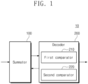
- FIG. 1 is a block diagram illustrating a decision feedback equalizer, according to an embodiment of the present disclosure.
- a decision feedback equalizer 10 may be implemented in a receiving device that receives a 4-Level Plus Amplitude Modulation (PAM-4) signal in Gray Code.
- the decision feedback equalizer 10 may be implemented in the receiving device of various devices such as desktop computers, laptop computers, tablet computers, smart phones, wearable devices, video game consoles, home appliances, medical devices, etc.
- the decision feedback equalizer 10 includes a summator 100 and a decoder 200.
- the summator 100 may receive a PAM-4 signal based on the Gray code and first and second bit signals, and may output an input voltage obtained by adding a preset coefficient to a voltage level of the PAM-4 signal in response to the first and second bit signals.
- the decoder 200 may receive the input voltage and first to third reference voltages of the PAM-4 signal, and may output the first and second bit signals. To this end, the decoder 200 includes a first comparator 210 and a second comparator 220.
- the first comparator 210 may compare a magnitude of the input voltage with a magnitude of the first reference voltage and may output the first bit signal as "0" or "1". For example, the first comparator 210 may output the first bit signal as "1" when the input voltage is greater than the first reference voltage, and may output the first bit signal as "0" when the input voltage is less than the first reference voltage.
- the second comparator 220 may compare charge-discharge intensities of the input voltage and the second and third reference voltages and may output the second bit signal as "0" or "1". For example, the second comparator 220 may output the second bit signal as "0" when the input voltage is greater than the second reference voltage and less than the third reference voltage, and may output the second bit signal as "1" when the input voltage is less than the second reference voltage and greater than the third reference voltage.
- FIGS. 4A and 4B A more detailed description of the first and second comparators 210 and 220 will be provided in FIGS. 4A and 4B .
- the decision feedback equalizer 10 may decode data through the first and second comparators 210 and 220 of the decoder 200, and the decoder 200 may feedback the first and second bit signals, which are Return-To-Zero (RZ) data, to the summator 100. Accordingly, the decoder 200 may reduce a feedback loop delay of the decoder 200 by omitting the additional process of converting to NRZ (Non-Return-To-Zero) data.
- RZ Return-To-Zero
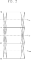
- FIG. 2 is a diagram describing first to third reference voltages of a PAM-4 signal, according to an embodiment of the present disclosure.
- the lowest first level of the PAM-4 signal may be mapped to 2-bit data '00', and the highest fourth level of the PAM-4 signal may be mapped to 2-bit data '10'.
- a second level of the PAM-4 signal may be mapped to 2-bit data '01', and a third level of the PAM-4 signal may be mapped to 2-bit data '11'.
- a first reference voltage VREF of the PAM-4 signal may be a voltage level between the second level and the third level
- a second reference voltage VREFP of the PAM-4 signal may be a voltage level between the third level and the fourth level
- a third reference voltage VREFN of the PAM-4 signal may be a voltage level between the first level and the second level.
- FIG. 3 is a block diagram illustrating an example of a comparator, according to an embodiment of the present disclosure.
- the decoder 200 may implement an even path and an odd path to decode a first bit signal MSB and a second bit signal LSB. Meanwhile, the even path and the odd path of the decoder 200 are the same path with the only difference being the bit signal. Therefore, hereinafter, for convenience of description, the odd path will be representatively described.
- the first comparator 210 of the odd path may output first odd bit signals MSB_ODD and MSBB_ODD for input voltages VINP and VINN in response to an odd clock signal CLK_ODD.
- the second comparator 220 of the odd path may output second odd bit signals LSB_ODD and LSBB_ODD for the input voltages VINP and VINN in response to the odd clock signal CLK_ODD.
- the decoder 200 may feedback the first odd bit signals MSB_ODD and MSBB_ODD and the second odd bit signals LSB _ODD and LSBB_ODD to the summator 100.
- the decoder 200 may convert the first odd bit signals MSB _ODD and MSBB_ODD and the second odd bit signals LSB _ODD and LSBB_ODD through an SR latch 230 to output odd decoding signals MSB_ODD_SR and LSB_ODD_SR.
- the decoder 200 distinguishes the odd path and the even path for the bit signal to facilitate an intuitive expression of the bit value of the PAM-4 signal and a signal recovery.
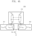
- FIGS. 4A and 4B are circuit diagrams illustrating an example of a comparator, according to embodiments of the present disclosure.
- FIG. 4A is a circuit diagram illustrating an example of the first comparator 210
- FIG. 4B is a circuit diagram illustrating an example of the second comparator 220.
- the first comparator 210 may be implemented with a first input terminal 211, a second input terminal 212, and a first output terminal 213.
- the first input terminal 211 may include a plurality of transistors including gates to which the positive input voltage VINP and the first reference voltage VREF are applied, respectively
- the second input terminal 212 may include a plurality of transistors including gates to which the negative input voltage VINN and the first reference voltage VREF are applied, respectively.
- the first comparator 210 may perform a comparison operation when a first transistor TR1 is turned on in response to a common signal. The first comparator 210 may receive the positive input voltage VINP and the first reference voltage VREF through the first input terminal 211.
- the first comparator 210 may receive the negative input voltage VINN and the first reference voltage VREF through the second input terminal 212.
- the first comparator 210 may compare the received information of the first input terminal 211 and the second input terminal 212 and may output the first bit signal MSB of "0" or "1" through the first output terminal 213. For example, when an input voltage VINP, VINN is greater than the first reference voltage VREF, the first comparator 210 may output the first bit signal MSB as "1", and when the input voltage VINP, VINN is less than the first reference voltage VREF, the first comparator 210 may output the first bit signal MSB as "0".
- the second comparator 220 may be implemented with a third input terminal 221, a fourth input terminal 222, and a second output terminal 223.
- the third input terminal 221 may include a plurality of transistors including gates to which the positive input voltage VINP and the negative input voltage VINN are applied, respectively
- the fourth input terminal 222 may include a plurality of transistors including gates to which the second reference voltage VREFP and the third reference voltage VREFN are applied, respectively.
- the second comparator 220 may perform a comparison operation when a second transistor TR2 is turned on in response to a common signal. The second comparator 220 may receive the positive input voltage VINP and the negative input voltage VINN through the third input terminal 221.
- the second comparator 220 may receive the second reference voltage VREFP and the third reference voltage VREFN through the fourth input terminal 222.
- the second comparator 220 may compare the received information of the third input terminal 221 and the fourth input terminal 222 and may output the second bit signal LSB as "0" or "1" through the second output terminal 223.
- the second comparator 220 may compare different charge-discharge intensities of the third input terminal 221 and the fourth input terminal 222 and may output the second bit signal as "0" or "1". For example, the second comparator 220 may output the second bit signal LSB as "0" when the input voltages VINP and VINN are greater than the second reference voltage VREFP and less than the third reference voltage VREFN. Additionally, the second comparator 220 may output the second bit signal LSB as "1" when the input voltages VINP and VINN are less than the second reference voltage VREFP and greater than the third reference voltage VREFN.
- the decoder 200 may output the first bit signal MSB by comparing the magnitude of the input voltages VINP and VINN with the magnitude of the first reference voltage VREF, and the decoder 200 may output the second bit signal LSB by comparing the charge-discharge intensities of the input voltages VINP and VINN and the second and third reference voltages VREFP and VREFN. Accordingly, the decoder 200 may minimize the number of comparators that output the first and second bit signals MSB and LSB and may implement a 1-stage structure that may perform a decision feedback equalization operation.
- FIG. 5 is a circuit diagram illustrating an example of a summator, according to an embodiment of the present disclosure.
- the summator 100 may output the input voltages VINP and VINN obtained by adding first to fourth coefficients to the voltage level of the PMA-4 signal in response to the first and second bit signals MSB and LSB.
- the summator 100 includes a first tap 110 and a second tap 120.
- the first tap 110 and the second tap 120 of the summator 100 are implemented with the same circuit except that bit signals are different from each other. Therefore, hereinafter, for convenience of description, the first tap 110 will be described as a representative example.
- the first tap 110 may output an even bit signals of the input voltages VINP and VINN obtained by adding the first to fourth coefficients to the voltage level of the PAM-4 signal using first and second even bit signals MSB_EVEN and LSB_EVEN.
- the first tap 110 may include a plurality of transistors including gates to which the first and second even bit signals MSB_EVEN and LSB_EVEN and operating voltages V1 and V2 are applied, respectively.
- the first tap 110 may add the first coefficient to the voltage level of the PAM-4 signal when the first and second even bit signals MSB_EVEN and LSB_EVEN are "1" and "0", respectively, and may add the second coefficient to the voltage level of the PAM-4 signal when the first and second even bit signals MSB_EVEN and LSB_EVEN are "1" and "1", respectively.
- the first tap 110 may add the third coefficient to the voltage level of the PAM-4 signal, and when the first and second even bit signals MSB_EVEN and LSB_EVEN are "0" and "0", respectively, the first tap 110 may add the fourth coefficient to the voltage level of the PAM-4 signal.
- the first to fourth coefficients which are added to the voltage level of the PAM-4 signal may be +3, +1, -1, and -3, respectively, but are not limited thereto.
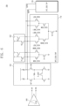
- FIG. 6 is a block diagram illustrating another embodiment of a decision feedback equalizer.
- FIG. 6 illustrates an example that further includes a continuous time linear equalizer 300, a variable gain amplifier 400, and a compensation circuit 500.
- the configuration of FIG. 7 other than the above configuration is similar to that of FIG. 5 . Therefore, the same or similar other component are denoted using the same or similar reference numerals, and additional descriptions will be omitted to avoid redundancy.
- a decision feedback equalizer 10A may further include the continuous time linear equalizer 300, the variable gain amplifier 400, and the compensation circuit 500.
- the continuous time linear equalizer 300 may receive a data signal from a transmitter, may amplify the magnitude of the high-frequency component of the data signal, and may generate a PAM-4 signal in which all frequency components of the data signal are uniformly equalized.
- the continuous time linear equalizer 300 may receive the data signal that may represent four data values 00, 01, 10, and 11 and may equalize the data signal by performing a sample/hold operation.
- the variable gain amplifier 400 may receive the PAM-4 signal from the continuous time linear equalizer 300 and may amplify intervals between the voltage level of the PAM-4 signal and the first to third reference voltages. For example, the variable gain amplifier 400 may adjust the voltage gain using a variable gain control signal R_CONT for controlling a variable resistance.
- the compensation circuit 500 may maintain the common mode uniform.
- the common mode of the overall circuit is reduced due to the summator 100 generating the charge-discharge. Accordingly, the compensation circuit 500 may maintain the common mode of the overall circuit uniform by pulling up the current applied to the summator 100 using a plurality of PMOS transistors.
- the compensation circuit 500 may include a plurality of PMOS transistors connected to a plurality of transistors of the first tap 110.
- the decision feedback equalizer 10A does not change the operating range of the circuit and may easily measure the voltage level of the PAM-4 signal and the first to third reference voltages.
- FIG. 7 is a flowchart illustrating an operation of a decision feedback equalizer, according to an embodiment of the present disclosure.
- the summator 100 may output the input voltages VINP and VINN obtained by adding a preset coefficient to the voltage level of the PAM-4 signal in response to the first and second bit signals MSB and LSB.
- the first comparator 210 of the decoder 200 may compare the magnitude of the input voltages VINP and VINN with the first reference voltage VREF and may output the first bit signal MSB.
- the second comparator 220 of the decoder 200 may compare the charge-discharge intensities of the input voltages VINP and VINN and the second and third reference voltages VREFP and VREFN to output the second bit signal LSB.
- the decoder 200 may output the first and second bit signals MSB and LSB, which are the RZ data, as even and odd signals, and may input the output bit signals to the summator 100.
- the decision feedback equalizer that minimizes the number of comparators in decoder may implement a decision feedback equalization circuit using the RZ signal. Accordingly, the present disclosure may reduce the power consumption of the overall circuit and may reduce the feedback loop delay.
Landscapes
- Engineering & Computer Science (AREA)
- Computer Networks & Wireless Communication (AREA)
- Signal Processing (AREA)
- Physics & Mathematics (AREA)
- Spectroscopy & Molecular Physics (AREA)
- Power Engineering (AREA)
- Cable Transmission Systems, Equalization Of Radio And Reduction Of Echo (AREA)
- Dc Digital Transmission (AREA)
Abstract
Disclosed is a decision feedback equalizer, which includes a summator that receives a gray code-based PAM-4 signal, a first bit signal, and a second bit signal, and outputs an input voltage obtained by adding a preset coefficient to a voltage level of the PAM-4 signal in response to the first bit signal and the second bit signal, and a decoder that receives the input voltage and first to third reference voltages of the PAM-4 signal and outputs the first bit signal and the second bit signal, and the decoder includes a first comparator that outputs the first bit signal by comparing a magnitude of the input voltage with a magnitude of the first reference voltage, and a second comparator that outputs the second bit signal by comparing charge-discharge intensities of the input voltage and the second and third reference voltages.
Description
- This application claims priority to
Korean Patent Application No. 10-2023-0096721 filed on July 25, 2023 - Embodiments of the present disclosure described herein relate to a decision feedback equalizer capable of minimizing the number of comparators in a PAM-4 decoder and an operation method thereof.
- Recently, as a transmission speed of wired transceivers has increased, the hardware cost to transmit high-speed clocks to entire chips is increasing, and power consumption is also increasing. Accordingly, technology using a multi-phase architecture is required for transceivers to process vast amounts of data signals transmitted at high speeds.
- To this end, the transceiver may include a continuous time linear equalizer, a decision feedback equalizer, etc. However, due to the increasing the number of comparators in the decoder, there are issues that power consumption in data paths and clock paths increases and a bandwidth is limited.
- Embodiments of the present disclosure provide a decision feedback equalizer for minimizing the number of comparators in a PAM-4 decoder and an operation method thereof.
- According to an embodiment of the present disclosure, a decision feedback equalizer includes a summator that receives a gray code-based PAM-4 signal, a first bit signal, and a second bit signal, and outputs an input voltage obtained by adding a preset coefficient to a voltage level of the PAM-4 signal in response to the first bit signal and the second bit signal, and a decoder that receives the input voltage and a first reference voltage, a second reference voltage, and a third reference voltage of the PAM-4 signal and outputs the first bit signal and the second bit signal, and the decoder includes a first comparator that outputs the first bit signal by comparing a magnitude of the input voltage with a magnitude of the first reference voltage, and a second comparator that outputs the second bit signal by comparing charge-discharge intensities of the input voltage and the second and third reference voltages.
- According to an embodiment, the second comparator, when the input voltage is greater than the second reference voltage and less than the third reference voltage, may output the second bit signal as "0", and the second comparator, when the input voltage is less than the second reference voltage and greater than the third reference voltage, may output the second bit signal as "1".
- According to an embodiment, the summator may include a first tap that outputs an odd signal of the input voltage using odd bits of the first and second bit signals, and a second tap that outputs an even signal of the input voltage using even bits of the first and second bit signals.
- According to an embodiment, the summator, when the first and second bit signals are "1 " and "0", respectively, may add a first coefficient to the voltage level of the PAM-4 signal, the summator, when the first and second bit signals are "1" and "1", respectively, may add a second coefficient to the voltage level of the PAM-4 signal, the summator, when the first and second bit signals are "0" and "1", respectively, may add a third coefficient to the voltage level of the PAM-4 signal, and the summator, when the first and second bit signals are "0" and "0", respectively, may add a fourth coefficient to the voltage level of the PAM-4 signal.
- According to an embodiment, the decision feedback equalizer may further include a continuous time linear equalizer that receives a data signal, uniformly equalizes all frequency components of the data signal, and outputs the PAM-4 signal, a variable gain amplifier that receives the PAM-4 signal and amplifies intervals between the voltage level of the PAM-4 signal and the first to third reference voltages, and a compensation circuit that keeps a common mode of the summator uniform.
- According to an embodiment of the present disclosure, a method of operating a decision feedback equalizer, includes receiving a gray code-based PAM-4 signal, a first bit signal, and a second bit signal, and outputting an input voltage obtained by adding a preset coefficient to a voltage level of the PAM-4 signal in response to the first bit signal and the second bit signal, and receiving the input voltage and first to third reference voltages of the PAM-4 signal, and outputting the first bit signal and the second bit signal, and the outputting of the first bit signal and the second bit signal includes outputting the first bit signal by comparing a magnitude of the input voltage with a magnitude of the first reference voltage, and outputting the second bit signal by comparing charge-discharge intensities of the input voltage and the second and third reference voltages.
- According to an embodiment, the outputting of the second bit signal, when the input voltage is greater than the second reference voltage and less than the third reference voltage, may include outputting the second bit signal as "0", and when the input voltage is less than the second reference voltage and greater than the third reference voltage, may include outputting the second bit signal as "1".
- According to an embodiment, the outputting of the input voltage may include outputting an odd signal of the input voltage using odd bits of the first and second bit signals, and outputting an even signal of the input voltage using even bits of the first and second bit signals.
- According to an embodiment, the outputting of the input voltage may include, when the first and second bit signals are "1" and "0", respectively, adding a first coefficient to the voltage level of the PAM-4 signal, when the first and second bit signals are "1" and "1", respectively, adding a second coefficient to the voltage level of the PAM-4 signal, when the first and second bit signals are "0" and "1", respectively, adding a third coefficient to the voltage level of the PAM-4 signal, and when the first and second bit signals are "0" and "0", respectively, adding a fourth coefficient to the voltage level of the PAM-4 signal.
- According to an embodiment, the method may further include receiving a data signal, uniformly equalizing all frequency components of the data signal, and outputting the PAM-4 signal, receiving the PAM-4 signal and amplifying intervals between the voltage level of the PAM-4 signal and the first to third reference voltages, and keeping a common mode of the outputting the input voltage uniform.
- The above and other objects and features of the present disclosure will become apparent by describing in detail embodiments thereof with reference to the accompanying drawings.
-
FIG. 1 is a block diagram illustrating a decision feedback equalizer, according to an embodiment of the present disclosure. -
FIG. 2 is a diagram describing first to third reference voltages of a PAM-4 signal, according to an embodiment of the present disclosure. -
FIG. 3 is a block diagram illustrating an example of a comparator, according to an embodiment of the present disclosure. -
FIGS. 4A and4B are circuit diagrams illustrating an example of a comparator, according to embodiments of the present disclosure. -
FIG. 5 is a circuit diagram illustrating an example of a summator, according to an embodiment of the present disclosure. -
FIG. 6 is a block diagram illustrating another embodiment of a decision feedback equalizer. -
FIG. 7 is a flowchart illustrating an operation of a decision feedback equalizer, according to an embodiment of the present disclosure. - Hereinafter, embodiments of the present disclosure will be described in detail and clearly to such an extent that an ordinary one in the art easily implements the present disclosure.
-
FIG. 1 is a block diagram illustrating a decision feedback equalizer, according to an embodiment of the present disclosure. - A
decision feedback equalizer 10 according to an embodiment of the present disclosure may be implemented in a receiving device that receives a 4-Level Plus Amplitude Modulation (PAM-4) signal in Gray Code. For example, thedecision feedback equalizer 10 may be implemented in the receiving device of various devices such as desktop computers, laptop computers, tablet computers, smart phones, wearable devices, video game consoles, home appliances, medical devices, etc. - To be described in more detail with reference to
FIG. 1 , thedecision feedback equalizer 10 according to an embodiment of the present disclosure includes asummator 100 and adecoder 200. - The
summator 100 may receive a PAM-4 signal based on the Gray code and first and second bit signals, and may output an input voltage obtained by adding a preset coefficient to a voltage level of the PAM-4 signal in response to the first and second bit signals. - The
decoder 200 may receive the input voltage and first to third reference voltages of the PAM-4 signal, and may output the first and second bit signals. To this end, thedecoder 200 includes afirst comparator 210 and asecond comparator 220. - The
first comparator 210 may compare a magnitude of the input voltage with a magnitude of the first reference voltage and may output the first bit signal as "0" or "1". For example, thefirst comparator 210 may output the first bit signal as "1" when the input voltage is greater than the first reference voltage, and may output the first bit signal as "0" when the input voltage is less than the first reference voltage. - The
second comparator 220 may compare charge-discharge intensities of the input voltage and the second and third reference voltages and may output the second bit signal as "0" or "1". For example, thesecond comparator 220 may output the second bit signal as "0" when the input voltage is greater than the second reference voltage and less than the third reference voltage, and may output the second bit signal as "1" when the input voltage is less than the second reference voltage and greater than the third reference voltage. A more detailed description of the first andsecond comparators FIGS. 4A and4B . - As described above, the
decision feedback equalizer 10 according to an embodiment of the present disclosure may decode data through the first andsecond comparators decoder 200, and thedecoder 200 may feedback the first and second bit signals, which are Return-To-Zero (RZ) data, to thesummator 100. Accordingly, thedecoder 200 may reduce a feedback loop delay of thedecoder 200 by omitting the additional process of converting to NRZ (Non-Return-To-Zero) data. -
FIG. 2 is a diagram describing first to third reference voltages of a PAM-4 signal, according to an embodiment of the present disclosure. - Referring to
FIG. 2 , the lowest first level of the PAM-4 signal may be mapped to 2-bit data '00', and the highest fourth level of the PAM-4 signal may be mapped to 2-bit data '10'. A second level of the PAM-4 signal may be mapped to 2-bit data '01', and a third level of the PAM-4 signal may be mapped to 2-bit data '11'. In addition, a first reference voltage VREF of the PAM-4 signal may be a voltage level between the second level and the third level, a second reference voltage VREFP of the PAM-4 signal may be a voltage level between the third level and the fourth level, and a third reference voltage VREFN of the PAM-4 signal may be a voltage level between the first level and the second level. The mapping between the first to fourth levels and data described above is a mapping according to the Gray Code method, this is only an example, and the mapping may be changed according to various purposes. -
FIG. 3 is a block diagram illustrating an example of a comparator, according to an embodiment of the present disclosure. - Referring to
FIG. 3 , thedecoder 200 may implement an even path and an odd path to decode a first bit signal MSB and a second bit signal LSB. Meanwhile, the even path and the odd path of thedecoder 200 are the same path with the only difference being the bit signal. Therefore, hereinafter, for convenience of description, the odd path will be representatively described. - The
first comparator 210 of the odd path may output first odd bit signals MSB_ODD and MSBB_ODD for input voltages VINP and VINN in response to an odd clock signal CLK_ODD. - The
second comparator 220 of the odd path may output second odd bit signals LSB_ODD and LSBB_ODD for the input voltages VINP and VINN in response to the odd clock signal CLK_ODD. - The
decoder 200 may feedback the first odd bit signals MSB_ODD and MSBB_ODD and the second odd bit signals LSB _ODD and LSBB_ODD to thesummator 100. In addition, thedecoder 200 may convert the first odd bit signals MSB _ODD and MSBB_ODD and the second odd bit signals LSB _ODD and LSBB_ODD through anSR latch 230 to output odd decoding signals MSB_ODD_SR and LSB_ODD_SR. - As described above, the
decoder 200 according to an embodiment of the present disclosure distinguishes the odd path and the even path for the bit signal to facilitate an intuitive expression of the bit value of the PAM-4 signal and a signal recovery. -
FIGS. 4A and4B are circuit diagrams illustrating an example of a comparator, according to embodiments of the present disclosure.FIG. 4A is a circuit diagram illustrating an example of thefirst comparator 210, andFIG. 4B is a circuit diagram illustrating an example of thesecond comparator 220. - Referring to
FIG. 4A , thefirst comparator 210 may be implemented with afirst input terminal 211, asecond input terminal 212, and afirst output terminal 213. For example, thefirst input terminal 211 may include a plurality of transistors including gates to which the positive input voltage VINP and the first reference voltage VREF are applied, respectively, and thesecond input terminal 212 may include a plurality of transistors including gates to which the negative input voltage VINN and the first reference voltage VREF are applied, respectively. In more detail, thefirst comparator 210 may perform a comparison operation when a first transistor TR1 is turned on in response to a common signal. Thefirst comparator 210 may receive the positive input voltage VINP and the first reference voltage VREF through thefirst input terminal 211. Additionally, thefirst comparator 210 may receive the negative input voltage VINN and the first reference voltage VREF through thesecond input terminal 212. Thefirst comparator 210 may compare the received information of thefirst input terminal 211 and thesecond input terminal 212 and may output the first bit signal MSB of "0" or "1" through thefirst output terminal 213. For example, when an input voltage VINP, VINN is greater than the first reference voltage VREF, thefirst comparator 210 may output the first bit signal MSB as "1", and when the input voltage VINP, VINN is less than the first reference voltage VREF, thefirst comparator 210 may output the first bit signal MSB as "0". - Referring to
FIG. 4B , thesecond comparator 220 may be implemented with athird input terminal 221, afourth input terminal 222, and asecond output terminal 223. For example, thethird input terminal 221 may include a plurality of transistors including gates to which the positive input voltage VINP and the negative input voltage VINN are applied, respectively, and thefourth input terminal 222 may include a plurality of transistors including gates to which the second reference voltage VREFP and the third reference voltage VREFN are applied, respectively. In more detail, thesecond comparator 220 may perform a comparison operation when a second transistor TR2 is turned on in response to a common signal. Thesecond comparator 220 may receive the positive input voltage VINP and the negative input voltage VINN through thethird input terminal 221. Additionally, thesecond comparator 220 may receive the second reference voltage VREFP and the third reference voltage VREFN through thefourth input terminal 222. Thesecond comparator 220 may compare the received information of thethird input terminal 221 and thefourth input terminal 222 and may output the second bit signal LSB as "0" or "1" through thesecond output terminal 223. - In more detail, the
second comparator 220 may compare different charge-discharge intensities of thethird input terminal 221 and thefourth input terminal 222 and may output the second bit signal as "0" or "1". For example, thesecond comparator 220 may output the second bit signal LSB as "0" when the input voltages VINP and VINN are greater than the second reference voltage VREFP and less than the third reference voltage VREFN. Additionally, thesecond comparator 220 may output the second bit signal LSB as "1" when the input voltages VINP and VINN are less than the second reference voltage VREFP and greater than the third reference voltage VREFN. - As described above, the
decoder 200 according to an embodiment of the present disclosure may output the first bit signal MSB by comparing the magnitude of the input voltages VINP and VINN with the magnitude of the first reference voltage VREF, and thedecoder 200 may output the second bit signal LSB by comparing the charge-discharge intensities of the input voltages VINP and VINN and the second and third reference voltages VREFP and VREFN. Accordingly, thedecoder 200 may minimize the number of comparators that output the first and second bit signals MSB and LSB and may implement a 1-stage structure that may perform a decision feedback equalization operation. -
FIG. 5 is a circuit diagram illustrating an example of a summator, according to an embodiment of the present disclosure. - Referring to
FIG. 5 , thesummator 100 may output the input voltages VINP and VINN obtained by adding first to fourth coefficients to the voltage level of the PMA-4 signal in response to the first and second bit signals MSB and LSB. To this end, thesummator 100 includes afirst tap 110 and asecond tap 120. Meanwhile, thefirst tap 110 and thesecond tap 120 of thesummator 100 are implemented with the same circuit except that bit signals are different from each other. Therefore, hereinafter, for convenience of description, thefirst tap 110 will be described as a representative example. - The
first tap 110 may output an even bit signals of the input voltages VINP and VINN obtained by adding the first to fourth coefficients to the voltage level of the PAM-4 signal using first and second even bit signals MSB_EVEN and LSB_EVEN. For example, thefirst tap 110 may include a plurality of transistors including gates to which the first and second even bit signals MSB_EVEN and LSB_EVEN and operating voltages V1 and V2 are applied, respectively. - The
first tap 110 according to an embodiment of the present disclosure may add the first coefficient to the voltage level of the PAM-4 signal when the first and second even bit signals MSB_EVEN and LSB_EVEN are "1" and "0", respectively, and may add the second coefficient to the voltage level of the PAM-4 signal when the first and second even bit signals MSB_EVEN and LSB_EVEN are "1" and "1", respectively. In addition, when the first and second even bit signals MSB_EVEN and LSB_EVEN are "0" and "1", respectively, thefirst tap 110 may add the third coefficient to the voltage level of the PAM-4 signal, and when the first and second even bit signals MSB_EVEN and LSB_EVEN are "0" and "0", respectively, thefirst tap 110 may add the fourth coefficient to the voltage level of the PAM-4 signal. In this case, the first to fourth coefficients which are added to the voltage level of the PAM-4 signal may be +3, +1, -1, and -3, respectively, but are not limited thereto. -
FIG. 6 is a block diagram illustrating another embodiment of a decision feedback equalizer. - In detail,
FIG. 6 illustrates an example that further includes a continuous timelinear equalizer 300, avariable gain amplifier 400, and acompensation circuit 500. The configuration ofFIG. 7 other than the above configuration is similar to that ofFIG. 5 . Therefore, the same or similar other component are denoted using the same or similar reference numerals, and additional descriptions will be omitted to avoid redundancy. - Referring to
FIG. 6 , adecision feedback equalizer 10A may further include the continuous timelinear equalizer 300, thevariable gain amplifier 400, and thecompensation circuit 500. - The continuous time
linear equalizer 300 may receive a data signal from a transmitter, may amplify the magnitude of the high-frequency component of the data signal, and may generate a PAM-4 signal in which all frequency components of the data signal are uniformly equalized. For example, the continuous timelinear equalizer 300 may receive the data signal that may represent fourdata values - The
variable gain amplifier 400 may receive the PAM-4 signal from the continuous timelinear equalizer 300 and may amplify intervals between the voltage level of the PAM-4 signal and the first to third reference voltages. For example, thevariable gain amplifier 400 may adjust the voltage gain using a variable gain control signal R_CONT for controlling a variable resistance. - The
compensation circuit 500 may maintain the common mode uniform. For example, in thedecision feedback equalizer 10A, the common mode of the overall circuit is reduced due to thesummator 100 generating the charge-discharge. Accordingly, thecompensation circuit 500 may maintain the common mode of the overall circuit uniform by pulling up the current applied to thesummator 100 using a plurality of PMOS transistors. For example, thecompensation circuit 500 may include a plurality of PMOS transistors connected to a plurality of transistors of thefirst tap 110. - As described above, the
decision feedback equalizer 10A does not change the operating range of the circuit and may easily measure the voltage level of the PAM-4 signal and the first to third reference voltages. -
FIG. 7 is a flowchart illustrating an operation of a decision feedback equalizer, according to an embodiment of the present disclosure. - Referring to
FIG. 7 , in operation S110, thesummator 100 may output the input voltages VINP and VINN obtained by adding a preset coefficient to the voltage level of the PAM-4 signal in response to the first and second bit signals MSB and LSB. - In operation S120, the
first comparator 210 of thedecoder 200 may compare the magnitude of the input voltages VINP and VINN with the first reference voltage VREF and may output the first bit signal MSB. - In operation S130, the
second comparator 220 of thedecoder 200 may compare the charge-discharge intensities of the input voltages VINP and VINN and the second and third reference voltages VREFP and VREFN to output the second bit signal LSB. - In operation S140, the
decoder 200 may output the first and second bit signals MSB and LSB, which are the RZ data, as even and odd signals, and may input the output bit signals to thesummator 100. - According to an embodiment of the present disclosure, the decision feedback equalizer that minimizes the number of comparators in decoder may implement a decision feedback equalization circuit using the RZ signal. Accordingly, the present disclosure may reduce the power consumption of the overall circuit and may reduce the feedback loop delay.
- The above descriptions are detail embodiments for carrying out the present disclosure. Embodiments in which a design is changed simply or which are easily changed may be included in the present disclosure as well as an embodiment described above. In addition, technologies that are easily changed and implemented by using the above embodiments may be included in the present disclosure. Therefore, the scope of the present disclosure should not be limited to the above-described embodiments and should be defined by not only the claims to be described later, but also those equivalent to the claims of the present disclosure.
- This work was supported by the National Research Foundation of Korea (NRF) grate funded by the Korea government (MSIT) (No. NRF-RS-2023-0281047).
Claims (10)
- A decision feedback equalizer comprising:a summator configured to receive a gray code-based PAM-4 signal, a first bit signal, and a second bit signal, and to output an input voltage obtained by adding a preset coefficient to a voltage level of the PAM-4 signal in response to the first bit signal and the second bit signal; anda decoder configured to receive the input voltage and a first reference voltage, a second reference voltage, and . to third reference voltages of the PAM-4 signal and to output the first bit signal and the second bit signal, andwherein the decoder includes:a first comparator configured to output the first bit signal by comparing a magnitude of the input voltage with a magnitude of the first reference voltage; anda second comparator configured to output the second bit signal by comparing charge-discharge intensities of the input voltage and the second and third reference voltages.
- The decision feedback equalizer of claim 1, wherein the second comparator is configured to:when the input voltage is greater than the second reference voltage and less than the third reference voltage, output the second bit signal as "0"; andwhen the input voltage is less than the second reference voltage and greater than the third reference voltage, output the second bit signal as "1".
- The decision feedback equalizer of claim 1, wherein the summator includes:a first tap configured to output an odd signal of the input voltage using odd bits of the first and second bit signals; anda second tap configured to output an even signal of the input voltage using even bits of the first and second bit signals.
- The decision feedback equalizer of claim 1, wherein the summator is configured to:when the first and second bit signals are "1" and "0", respectively, add a first coefficient to the voltage level of the PAM-4 signal;when the first and second bit signals are "1" and "1", respectively, add a second coefficient to the voltage level of the PAM-4 signal;when the first and second bit signals are "0" and "1", respectively, add a third coefficient to the voltage level of the PAM-4 signal; andwhen the first and second bit signals are "0" and "0", respectively, add a fourth coefficient to the voltage level of the PAM-4 signal.
- The decision feedback equalizer of claim 1, further comprising:a continuous time linear equalizer configured to receive a data signal, to uniformly equalize all frequency components of the data signal, and to output the PAM-4 signal;a variable gain amplifier configured to receive the PAM-4 signal and to amplify intervals between the voltage level of the PAM-4 signal and the first to third reference voltages; anda compensation circuit configured to keep a common mode of the summator uniform.
- A method of operating a decision feedback equalizer, the method comprising:receiving a gray code-based PAM-4 signal, a first bit signal, and a second bit signal, and outputting an input voltage obtained by adding a preset coefficient to a voltage level of the PAM-4 signal in response to the first bit signal and the second bit signal; andreceiving the input voltage and first to third reference voltages of the PAM-4 signal, and outputting the first bit signal and the second bit signal, andwherein the outputting of the first bit signal and the second bit signal includes:outputting the first bit signal by comparing a magnitude of the input voltage with a magnitude of the first reference voltage; andoutputting the second bit signal by comparing charge-discharge intensities of the input voltage and the second and third reference voltages.
- The method of claim 6, wherein the outputting of the second bit signal includes:when the input voltage is greater than the second reference voltage and less than the third reference voltage, outputting the second bit signal as "0"; andwhen the input voltage is less than the second reference voltage and greater than the third reference voltage, outputting the second bit signal as "1".
- The method of claim 6, wherein the outputting of the input voltage includes:outputting an odd signal of the input voltage using odd bits of the first and second bit signals; andoutputting an even signal of the input voltage using even bits of the first and second bit signals.
- The method of claim 6, wherein the outputting of the input voltage includes:when the first and second bit signals are "1" and "0", respectively, adding a first coefficient to the voltage level of the PAM-4 signal;when the first and second bit signals are "1" and "1", respectively, adding a second coefficient to the voltage level of the PAM-4 signal;when the first and second bit signals are "0" and "1", respectively, adding a third coefficient to the voltage level of the PAM-4 signal; andwhen the first and second bit signals are "0" and "0", respectively, adding a fourth coefficient to the voltage level of the PAM-4 signal.
- The method of claim 6, further comprising:receiving a data signal, uniformly equalizing all frequency components of the data signal, and outputting the PAM-4 signal;receiving the PAM-4 signal and amplifying intervals between the voltage level of the PAM-4 signal and the first to third reference voltages; andkeeping a common mode of the outputting the input voltage uniform.
Applications Claiming Priority (1)
| Application Number | Priority Date | Filing Date | Title |
|---|---|---|---|
| KR1020230096721A KR102766806B1 (en) | 2023-07-25 | 2023-07-25 | Decision feedback equalizer minimizing the number of comparators in decoder and its operation method therof |
Publications (1)
| Publication Number | Publication Date |
|---|---|
| EP4498645A1 true EP4498645A1 (en) | 2025-01-29 |
Family
ID=92043040
Family Applications (1)
| Application Number | Title | Priority Date | Filing Date |
|---|---|---|---|
| EP24190937.3A Pending EP4498645A1 (en) | 2023-07-25 | 2024-07-25 | Decision feedback equalizer for minimizing number of comparators in decoder and operation method thereof |
Country Status (3)
| Country | Link |
|---|---|
| EP (1) | EP4498645A1 (en) |
| JP (1) | JP2025019015A (en) |
| KR (1) | KR102766806B1 (en) |
Citations (1)
| Publication number | Priority date | Publication date | Assignee | Title |
|---|---|---|---|---|
| KR20230096721A (en) | 2021-12-23 | 2023-06-30 | 광성기업 주식회사 | Polylactic acid resin composition and its manufacturing method |
Family Cites Families (8)
| Publication number | Priority date | Publication date | Assignee | Title |
|---|---|---|---|---|
| KR101872310B1 (en) | 2011-12-19 | 2018-07-02 | 에스케이하이닉스 주식회사 | Rail-to-Rail Comparator and Pulse Amplitude Modulation Receiver and Communication System Using the Same |
| US9473330B1 (en) * | 2015-06-05 | 2016-10-18 | International Business Machines Corporation | Continuous time linear equalizer with a programmable negative feedback amplification loop |
| US10097383B1 (en) * | 2017-08-02 | 2018-10-09 | International Business Machines Corporation | High speed DFEs with direct feedback |
| CN111684715B (en) * | 2018-02-08 | 2023-05-02 | 株式会社索思未来 | Amplifying circuit, adding circuit, receiving circuit and integrated circuit |
| JP2020048060A (en) * | 2018-09-19 | 2020-03-26 | キオクシア株式会社 | Semiconductor integrated circuit, receiving device, and communication system |
| US11018656B1 (en) * | 2019-11-21 | 2021-05-25 | Credo Technology Group Limited | Multi-function level finder for serdes |
| KR102949118B1 (en) * | 2020-10-16 | 2026-04-03 | 삼성전자주식회사 | A receiver for data signal based on pulse amplitude modulation and an electronic device including the same |
| KR102478277B1 (en) * | 2021-06-25 | 2022-12-15 | 고려대학교 산학협력단 | 4 level pulse amplifier modulation receiver |
-
2023
- 2023-07-25 KR KR1020230096721A patent/KR102766806B1/en active Active
-
2024
- 2024-07-24 JP JP2024118868A patent/JP2025019015A/en active Pending
- 2024-07-25 EP EP24190937.3A patent/EP4498645A1/en active Pending
Patent Citations (1)
| Publication number | Priority date | Publication date | Assignee | Title |
|---|---|---|---|---|
| KR20230096721A (en) | 2021-12-23 | 2023-06-30 | 광성기업 주식회사 | Polylactic acid resin composition and its manufacturing method |
Non-Patent Citations (3)
| Title |
|---|
| CHEN KUAN-CHANG ET AL: "A 60-Gb/s PAM4 Wireline Receiver With 2-Tap Direct Decision Feedback Equalization Employing Track-and-Regenerate Slicers in 28-nm CMOS", IEEE JOURNAL OF SOLID-STATE CIRCUITS, IEEE, USA, vol. 56, no. 3, 6 October 2020 (2020-10-06), pages 750 - 762, XP011839886, ISSN: 0018-9200, [retrieved on 20210223], DOI: 10.1109/JSSC.2020.3025285 * |
| SIM JINCHEOL ET AL: "PAM-4 Receiver With 1-Tap DFE Using Clocked Comparator Offset Instead of Threshold Voltages for Improved LSB BER Performance", IEEE TRANSACTIONS ON CIRCUITS AND SYSTEMS I: REGULAR PAPERS, IEEE, US, vol. 70, no. 5, 1 May 2023 (2023-05-01), pages 1907 - 1916, XP011939583, ISSN: 1549-8328, [retrieved on 20230214], DOI: 10.1109/TCSI.2023.3241929 * |
| ZHU GUANG ET AL: "A low-power PAM4 receiver using 1/4-rate sampling decoder with adaptive variable-gain rectification", 2017 IEEE ASIAN SOLID-STATE CIRCUITS CONFERENCE (A-SSCC), IEEE, 6 November 2017 (2017-11-06), pages 81 - 84, XP033280863, DOI: 10.1109/ASSCC.2017.8240221 * |
Also Published As
| Publication number | Publication date |
|---|---|
| KR20250015376A (en) | 2025-02-03 |
| US20250039020A1 (en) | 2025-01-30 |
| KR102766806B1 (en) | 2025-02-11 |
| JP2025019015A (en) | 2025-02-06 |
Similar Documents
| Publication | Publication Date | Title |
|---|---|---|
| TWI698105B (en) | Low power high speed receiver with reduced decision feedback equalizer samplers | |
| CN107919873B (en) | Receiving circuit and semiconductor integrated circuit | |
| US9319061B1 (en) | Apparatus and methods for active termination of digital-to-analog converters | |
| KR20090049290A (en) | Multi-Level Pulse Amplitude Modulation Transceiver and Data Transmission / Reception Method | |
| US8416840B2 (en) | Duobinary transceiver | |
| KR102478277B1 (en) | 4 level pulse amplifier modulation receiver | |
| US11784855B2 (en) | Adaptive receiver with pre-cursor cancelation | |
| US11539390B2 (en) | Semiconductor integrated circuit and reception device | |
| US10171273B2 (en) | Decision feedback equalizer and interconnect circuit | |
| US12237949B2 (en) | Communication receiver using multi-stage channel equalization and associated method | |
| US10644911B1 (en) | Multi-level pulse-amplitude modulation receiver system | |
| US10348536B2 (en) | Data transmission device for modulating amplitude of PAM-4 signal using toggle serializer and method of operating the same | |
| US12634176B2 (en) | Decision feedback equalizer for minimizing number of comparators in decoder and operation method thereof | |
| US20250039020A1 (en) | Decision feedback equalizer for minimizing number of comparators in decoder and operation method thereof | |
| KR102747805B1 (en) | Decision feedback equalizer outputting thermometer code and its operation method thereof | |
| US20080212718A1 (en) | Multi-Rate Tracking Circuit | |
| TW202030990A (en) | Integrated circuit | |
| KR102636015B1 (en) | Pam-8 transceiver using differential mode pam-4 and common mode nrz and transceive method therefor | |
| KR20250088387A (en) | Pam-3 transceiver including multiple equalization methods for multi-voltage levels | |
| EP3635861B1 (en) | Three-input continuous-time amplifier and equalizer for multi-level signaling | |
| US20240223417A1 (en) | Equalizer including an amplifying adder and receiver comprising the equalizer | |
| TWI925209B (en) | Multi-level pulse amplitude modulation receiving device and all transition phase detector thereof | |
| KR102740335B1 (en) | Apparatus and method of ZQ Calibration of PAM Driver for Memory interface | |
| KR102935895B1 (en) | Voltage-Time Converter and Receiver including the Voltage-Time Converter | |
| US20240413834A1 (en) | Voltage-to-time converters and methods of operating same |
Legal Events
| Date | Code | Title | Description |
|---|---|---|---|
| PUAI | Public reference made under article 153(3) epc to a published international application that has entered the european phase |
Free format text: ORIGINAL CODE: 0009012 |
|
| STAA | Information on the status of an ep patent application or granted ep patent |
Free format text: STATUS: REQUEST FOR EXAMINATION WAS MADE |
|
| 17P | Request for examination filed |
Effective date: 20240725 |
|
| AK | Designated contracting states |
Kind code of ref document: A1 Designated state(s): AL AT BE BG CH CY CZ DE DK EE ES FI FR GB GR HR HU IE IS IT LI LT LU LV MC ME MK MT NL NO PL PT RO RS SE SI SK SM TR |