EP4498537A1 - Laser light source module and projection apparatus having the same - Google Patents
Laser light source module and projection apparatus having the same Download PDFInfo
- Publication number
- EP4498537A1 EP4498537A1 EP24156479.8A EP24156479A EP4498537A1 EP 4498537 A1 EP4498537 A1 EP 4498537A1 EP 24156479 A EP24156479 A EP 24156479A EP 4498537 A1 EP4498537 A1 EP 4498537A1
- Authority
- EP
- European Patent Office
- Prior art keywords
- laser
- light beam
- light
- wedge
- inclined surface
- Prior art date
- Legal status (The legal status is an assumption and is not a legal conclusion. Google has not performed a legal analysis and makes no representation as to the accuracy of the status listed.)
- Pending
Links
Images






Classifications
-
- G—PHYSICS
- G02—OPTICS
- G02B—OPTICAL ELEMENTS, SYSTEMS OR APPARATUS
- G02B27/00—Optical systems or apparatus not provided for by any of the groups G02B1/00 - G02B26/00, G02B30/00
- G02B27/09—Beam shaping, e.g. changing the cross-sectional area, not otherwise provided for
- G02B27/0916—Adapting the beam shape of a semiconductor light source such as a laser diode or an LED, e.g. for efficiently coupling into optical fibers
- G02B27/0922—Adapting the beam shape of a semiconductor light source such as a laser diode or an LED, e.g. for efficiently coupling into optical fibers the semiconductor light source comprising an array of light emitters
-
- G—PHYSICS
- G03—PHOTOGRAPHY; CINEMATOGRAPHY; ANALOGOUS TECHNIQUES USING WAVES OTHER THAN OPTICAL WAVES; ELECTROGRAPHY; HOLOGRAPHY
- G03B—APPARATUS OR ARRANGEMENTS FOR TAKING PHOTOGRAPHS OR FOR PROJECTING OR VIEWING THEM; APPARATUS OR ARRANGEMENTS EMPLOYING ANALOGOUS TECHNIQUES USING WAVES OTHER THAN OPTICAL WAVES; ACCESSORIES THEREFOR
- G03B21/00—Projectors or projection-type viewers; Accessories therefor
- G03B21/14—Details
- G03B21/20—Lamp housings
- G03B21/2006—Lamp housings characterised by the light source
- G03B21/2033—LED or laser light sources
-
- G—PHYSICS
- G02—OPTICS
- G02B—OPTICAL ELEMENTS, SYSTEMS OR APPARATUS
- G02B27/00—Optical systems or apparatus not provided for by any of the groups G02B1/00 - G02B26/00, G02B30/00
- G02B27/09—Beam shaping, e.g. changing the cross-sectional area, not otherwise provided for
- G02B27/0927—Systems for changing the beam intensity distribution, e.g. Gaussian to top-hat
-
- G—PHYSICS
- G02—OPTICS
- G02B—OPTICAL ELEMENTS, SYSTEMS OR APPARATUS
- G02B27/00—Optical systems or apparatus not provided for by any of the groups G02B1/00 - G02B26/00, G02B30/00
- G02B27/10—Beam splitting or combining systems
- G02B27/1006—Beam splitting or combining systems for splitting or combining different wavelengths
-
- G—PHYSICS
- G02—OPTICS
- G02B—OPTICAL ELEMENTS, SYSTEMS OR APPARATUS
- G02B27/00—Optical systems or apparatus not provided for by any of the groups G02B1/00 - G02B26/00, G02B30/00
- G02B27/10—Beam splitting or combining systems
- G02B27/12—Beam splitting or combining systems operating by refraction only
- G02B27/126—The splitting element being a prism or prismatic array, including systems based on total internal reflection
-
- G—PHYSICS
- G02—OPTICS
- G02B—OPTICAL ELEMENTS, SYSTEMS OR APPARATUS
- G02B27/00—Optical systems or apparatus not provided for by any of the groups G02B1/00 - G02B26/00, G02B30/00
- G02B27/18—Optical systems or apparatus not provided for by any of the groups G02B1/00 - G02B26/00, G02B30/00 for optical projection, e.g. combination of mirror and condenser and objective
-
- G—PHYSICS
- G02—OPTICS
- G02B—OPTICAL ELEMENTS, SYSTEMS OR APPARATUS
- G02B6/00—Light guides; Structural details of arrangements comprising light guides and other optical elements, e.g. couplings
- G02B6/24—Coupling light guides
- G02B6/42—Coupling light guides with opto-electronic elements
- G02B6/4201—Packages, e.g. shape, construction, internal or external details
- G02B6/4204—Packages, e.g. shape, construction, internal or external details the coupling comprising intermediate optical elements, e.g. lenses, holograms
- G02B6/4206—Optical features
-
- G—PHYSICS
- G03—PHOTOGRAPHY; CINEMATOGRAPHY; ANALOGOUS TECHNIQUES USING WAVES OTHER THAN OPTICAL WAVES; ELECTROGRAPHY; HOLOGRAPHY
- G03B—APPARATUS OR ARRANGEMENTS FOR TAKING PHOTOGRAPHS OR FOR PROJECTING OR VIEWING THEM; APPARATUS OR ARRANGEMENTS EMPLOYING ANALOGOUS TECHNIQUES USING WAVES OTHER THAN OPTICAL WAVES; ACCESSORIES THEREFOR
- G03B21/00—Projectors or projection-type viewers; Accessories therefor
- G03B21/14—Details
- G03B21/20—Lamp housings
- G03B21/2006—Lamp housings characterised by the light source
- G03B21/2013—Plural light sources
-
- G—PHYSICS
- G03—PHOTOGRAPHY; CINEMATOGRAPHY; ANALOGOUS TECHNIQUES USING WAVES OTHER THAN OPTICAL WAVES; ELECTROGRAPHY; HOLOGRAPHY
- G03B—APPARATUS OR ARRANGEMENTS FOR TAKING PHOTOGRAPHS OR FOR PROJECTING OR VIEWING THEM; APPARATUS OR ARRANGEMENTS EMPLOYING ANALOGOUS TECHNIQUES USING WAVES OTHER THAN OPTICAL WAVES; ACCESSORIES THEREFOR
- G03B21/00—Projectors or projection-type viewers; Accessories therefor
- G03B21/14—Details
- G03B21/20—Lamp housings
- G03B21/206—Control of light source other than position or intensity
-
- G—PHYSICS
- G03—PHOTOGRAPHY; CINEMATOGRAPHY; ANALOGOUS TECHNIQUES USING WAVES OTHER THAN OPTICAL WAVES; ELECTROGRAPHY; HOLOGRAPHY
- G03B—APPARATUS OR ARRANGEMENTS FOR TAKING PHOTOGRAPHS OR FOR PROJECTING OR VIEWING THEM; APPARATUS OR ARRANGEMENTS EMPLOYING ANALOGOUS TECHNIQUES USING WAVES OTHER THAN OPTICAL WAVES; ACCESSORIES THEREFOR
- G03B21/00—Projectors or projection-type viewers; Accessories therefor
- G03B21/14—Details
- G03B21/20—Lamp housings
- G03B21/208—Homogenising, shaping of the illumination light
-
- H—ELECTRICITY
- H01—ELECTRIC ELEMENTS
- H01S—DEVICES USING THE PROCESS OF LIGHT AMPLIFICATION BY STIMULATED EMISSION OF RADIATION [LASER] TO AMPLIFY OR GENERATE LIGHT; DEVICES USING STIMULATED EMISSION OF ELECTROMAGNETIC RADIATION IN WAVE RANGES OTHER THAN OPTICAL
- H01S5/00—Semiconductor lasers
- H01S5/005—Optical components external to the laser cavity, specially adapted therefor, e.g. for homogenisation or merging of the beams or for manipulating laser pulses, e.g. pulse shaping
-
- H—ELECTRICITY
- H01—ELECTRIC ELEMENTS
- H01S—DEVICES USING THE PROCESS OF LIGHT AMPLIFICATION BY STIMULATED EMISSION OF RADIATION [LASER] TO AMPLIFY OR GENERATE LIGHT; DEVICES USING STIMULATED EMISSION OF ELECTROMAGNETIC RADIATION IN WAVE RANGES OTHER THAN OPTICAL
- H01S5/00—Semiconductor lasers
- H01S5/02—Structural details or components not essential to laser action
- H01S5/022—Mountings; Housings
- H01S5/0225—Out-coupling of light
- H01S5/02251—Out-coupling of light using optical fibres
Definitions
- the present invention relates to a laser light source module and projection apparatus.
- Common light sources of projector include UHP lamp, LED, laser phosphor, and pure laser.
- the pure laser has advantages such as long life-span, high brightness, and good color saturation. Due to the breakthrough of high power semiconductor laser technology, pure laser becomes a dominant laser light source.
- the red laser has lower power due to wavelength property and development level. If the number of red light source is increased for enhancing red laser output power, the optical design becomes complicated and the light receiving area becomes larger, which increases the production cost.
- the invention provides a laser light source module.
- the laser light source module includes a laser chip, a wedge structure, a plano-convex lens, and an optical fiber.
- the laser chip is configured to emit a first light beam and a second light beam.
- the wedge structure is configured to refract the first light beam and the second light beam into a third light beam and make the first light beam and the second light beam overlap each other.
- the wedge structure is located between the laser chip and the plano-convex lens.
- the plano-convex lens is located between the wedge structure and the optical fiber.
- the laser chip is a red semiconductor laser chip of multiple resonant cavities.
- the optical fiber includes a light receiving surface
- the plano-convex lens is configured to focus the third light beam from the wedge structure to form a fifth light beam
- the light receiving surface is configured to receive the fifth light beam
- the laser chip includes a light-emitting surface, a first resonant cavity, and a second resonant cavity, the first resonant cavity emits the first light, the second resonant cavity emits the second light, the wedge structure includes a first plane, a first inclined surface, and a second inclined surface, the first plane faces the light-emitting surface of the laser chip, the first inclined surface and the second inclined surface face the plano-convex lens and are opposite to the first plane, and the first light beam and the second light beam pass through the first inclined surface and the second inclined surface, respectively.
- the laser chip further includes a third resonant cavity located between the first resonant cavity and the second resonant cavity, the third resonant cavity emits a fourth light beam
- the wedge structure includes a second plane, the second plane connects the first inclined surface and the second inclined surface and is opposite to the first plane, the fourth light beam passes through the second plane, and the first inclined surface and the second inclined surface of the wedge structure are configured to refract the first light beam and the second light beam towards the fourth light beam and make the first light beam and the second light beam to overlap each other.
- a number of the at least one laser chip is plural, a number of the at least one wedge structure is plural, the wedge structures correspond to the laser chips respectively, the laser chips form at least one laser array, and the wedge structures form at least one wedge array.
- the wedge structures of the wedge array are connected together.
- each one of the laser chips includes the first resonant cavity and the second resonant cavity arranged along a first direction, the first inclined surfaces and the second inclined surfaces of the wedge structures are alternately arranged along the first direction, each one of the first inclined surfaces of the wedge structures is configured to refract more than one of the first light beams, and each one of the second inclined surfaces of the wedge structures is configured to refract more than one of the second light beams.
- first inclined surface and the second inclined surface of each one of the wedge structures have an angle therebetween, and the angles of the wedge structures are the same.
- Another aspect of the present disclosure is a projection apparatus.
- the projection apparatus includes a laser light source module and a projection module.
- the projection module connects the laser light source module.
- the laser light source module includes a first laser chip, a second laser chip, a third laser chip, a wedge structure, and a plano-convex lens.
- the first laser chip is configured to emit a first light beam and a second light beam.
- the wedge structure is configured to refract the first light beam and the second light beam into a third light beam and make the first light beam and the second light beam overlap each other.
- the wedge structure is located between the first laser chip and the plano-convex lens.
- the laser light source module further includes an optical fiber, and the plano-convex lens is located between the wedge structure and the optical fiber.
- the first laser chip, the second laser chip, and the third laser chip are semiconductor lasers and are configured to emit laser lights with different wavelengths.
- the first laser chip is a semiconductor laser chip of multiple resonant cavities
- the second laser chip and the third laser chip are semiconductor laser chips of single resonant cavity.
- the first laser chip is a red semiconductor laser chip
- the first laser chip includes a light-emitting surface, a first resonant cavity, and a second resonant cavity
- the first resonant cavity emits the first light beam
- the second resonant cavity emits the second light beam
- the wedge structure includes a first plane, a first inclined surface, and a second inclined surface
- the first plane faces the light-emitting surface of the first laser chip
- the first inclined surface and the second inclined surface face the plano-convex lens and are opposite to the first plane
- the first light beam and the second light beam pass through the first inclined surface and the second inclined surface, respectively.
- the first laser chip further includes a third resonant cavity located between the first resonant cavity and the second resonant cavity, the third resonant cavity emits a fourth light beam
- the wedge structure further includes a second plane, the second plane connects the first inclined surface and the second inclined surface and are opposite to the first plane, the fourth light beam passes through the second plane, and the first inclined surface and the second inclined surface of the wedge structure are configured to respectively refract the first light beam and the second light beam towards the fourth light beam and make the first light beam and the second light beam overlap each other.
- a number of the at least one first laser chip is plural, a number of the at least one wedge structure is plural, the wedge structures correspond to the first laser chips respectively, the first laser chips form at least one laser array, and the wedge structures form at least one wedge array.
- each one of the first laser chips includes the first resonant cavity and the second resonant cavity arranged along a first direction, the first inclined surfaces and the second inclined surfaces of the wedge structures are alternately arranged along the first direction, each one of the first inclined surfaces of the wedge structures are configured to refract more than one of the first light beams, and each one of the second inclined surfaces of the wedge structures are configured to refract more than one of the second light beams.
- first inclined surface and the second inclined surface of each one of the wedge structures have an angle therebetween, and the angles of the wedge structures are the same.
- a number of the second laser chip is plural, the second laser chips form multiple second laser array, a number of the at least one third laser chip is plural, the third laser chips form a third laser array, the first laser chips are red semiconductor laser chips, the second laser chips are green semiconductor laser chips, and the third laser chips are blue semiconductor laser chips.
- the wedge structure is configured to refract the light beams from the dual resonant cavities (or multiple resonant cavities) and make them overlap each other to form a single light beam.
- the light receiving range of the light receiving surface of the optical fiber can be reduced to cut production cost.
- Such design enables the laser light source module be applied in a projection system having small light receiving area. The laser light source module can reduce light receiving area, cut production cost and remain the light receiving efficiency simultaneously.
- Fig. 1 is a schematic of a projection apparatus 10 according to one embodiment of the present disclosure.
- Fig. 2 is a schematic of the laser light source module 100 in Fig. 1 . Reference is made to Fig. 1 and Fig. 2 simultaneously.
- the projection apparatus 10 includes a laser light source module 100 and a projection module 200.
- the laser light source module 100 includes a first laser array 110, a second laser array 120, a third laser array 130, a wedge array 140, a plano-convex lens 150, and an optical fiber 160.
- the laser light source module 100 connects the projection module 200 through the optical fiber 160 and to transmit light signal.
- the laser light source module 100 is a semiconductor laser.
- the first laser array 110 includes multiple first laser chips 112.
- the second laser array 120 includes multiple second laser chips 122.
- the third laser array 130 includes multiple third laser chips 132.
- the first laser chips 112, the second laser chips 122, and the third laser chips 132 are configured to emit laser lights with different wavelengths.
- the first laser array 110 is a red semiconductor laser
- the second laser array 120 is a green semiconductor laser
- the third laser array 130 is a blue semiconductor laser.
- the wedge array 140 is located between the first laser array 110 and the plano-convex lens 150.
- the wedge array 140 is configured to refract a red light R from the first laser array 110 and is accompanied by the plano-convex lens 150 to make the multiple laser light beams from the first laser chip 112 overlap each other so as to shrink the light spot and increase the red light R receiving efficiency of the optical fiber 160.
- the output power of the red laser optical fiber is enhanced, and the power of the laser light source module 100 of different wavelengths can be balanced.
- the laser light source module 100 further includes a first dichroic filter 170 and a second dichroic filter 180.
- the first dichroic filter 170 is located between the second laser array 120 and the third laser array 130.
- the first dichroic filter 170 reflects the green light G from the second laser array 120, and enables the transmittance of the blue light B from the third laser array 130.
- the second dichroic filter 180 is located between the wedge array 140 and the plano-convex lens 150.
- the second dichroic filter 180 reflects the green light G from the second laser array 120 and the blue light B from the third laser array 130, and enables the transmittance the red light R which is from the first laser array 110 and been refracted by the wedge array 140.
- the relative positions of the first laser array 110, the second laser array 120, the third laser array 130, the first dichroic filter 170, and the second dichroic filter 180 are not limited as demonstrated herein, as long as the different laser lights can enter the optical fiber 160.
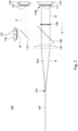
- Fig. 3 is a partial schematic of the laser light source module 100 in Fig. 2 .
- the first laser array 110, the wedge array 140, the plano-convex lens 150, and the optical fiber 160 are sequentially arranged along the direction of the optical axis A, but the present disclosure is not limited thereto.
- the plano-convex lens 150 is located between the wedge array 140 and the optical fiber 160.
- the first laser array 110 includes a light-emitting surface 110S.
- the light-emitting surface 110S faces the wedge array 140. In other words, a normal direction of the light-emitting surface 110S is parallel with the direction of the optical axis A.
- the normal direction of the light-emitting surface 110S is not parallel with the direction of the optical axis A, and the light passed through the wedge array 140 can be transmit to the plano-convex lens 150 through other optical element.
- the optical fiber 160 has a light receiving surface 162. The light receiving surface 162 faces the plano-convex lens 150.
- Fig. 4 is an enlarged view of the first laser array 110 in Fig. 3 .
- the multiple first laser chips 112 form a first laser array 110 having seven rows and four columns, but the present disclosure is not limited thereto.
- the concrete structures of the first laser chip 112 will be described in the following paragraphs.
- the first laser array 110 has a focusing lens 114 facing the wedge array 140, and each one of the first laser chip 112 corresponds to a single focusing lens 114.
- There are 28 focusing lens 114 in this embodiment which collectively form a lens array of the first laser array 110.
- Fig. 5 is an enlarged view of the wedge array 140 in Fig. 3 .
- the wedge array 140 includes multiple wedge structures 142 (the region labeled by the dashed frame).
- Each wedge structures 142 in Fig. 5 correspond to each first laser chips 112 in Fig. 4 .
- there are 28 wedge structures 142 which form a wedge array 140 having seven rows and four columns.
- the wedge structures 142 that are located at the same row are connected together.
- the wedge array 140 of the present embodiment can be considered as seven strip shape wedge structures each formed by four wedge structures 142 at the same row, and then those seven strip shape wedge structures arranged along the first direction D1 are connected to form the wedge array 140.
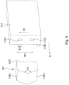
- Fig. 6 is a schematic of the first laser chip 112 and the wedge structure 142 according to one embodiment of the present disclosure.
- Fig. 7 is a light path schematic of the light beam from the first laser chip 112 passes through the wedge structure 142 in Fig. 6 . Reference is made to Fig. 6 and Fig. 7 .
- the focusing lens 114 is omitted in Fig. 6
- Fig. 7 is a side view.
- the first laser chip 112 is a semiconductor laser chip of dual resonant cavities (dual emitter).
- the first laser chip 112 has a first resonant cavity 1122 and a second resonant cavity 1124 arranged along the first direction D1.
- the first direction D1 is perpendicular to the direction of optical axis A, and the first direction D1 is perpendicular to the normal direction of the light-emitting surface 110S.
- the first direction D1 is a vertical direction.
- the first resonant cavity 1122 and the second resonant cavity 1124 can be arranged along the horizontal direction.
- a width W1 between the first resonant cavity 1122 and the second resonant cavity 1124 of the present embodiment is about 270 um, and an opening width W2 of the first resonant cavity 1122 and the second resonant cavity 1124 is about 75 um, but the present disclosure is not limited thereto.
- the wedge structure 142 includes a first plane 1422, a first inclined surface 1424 and a second inclined surface 1426.
- the first plane 1422 faces the light-emitting surface 110S of the first laser chip 112.
- the first inclined surface 1424 and the second inclined surface 1426 are opposite to the first plane 1422 and face the plano-convex lens 150 (see Fig. 3 ).
- the first inclined surface 1424 and the second inclined surface 1426 have an angle ⁇ 1 therebetween.
- the first resonant cavity 1122 emits the first light beam L1
- the second resonant cavity 1124 emits the second light beam L2.
- the first light beam L1 and the second light beam L2 are red lights.
- the first light beam L1 and the second light beam L2 pass through the focusing lens 114 and travel towards the wedge structure 142.
- the first light beam L1 and the second light beam L2 respectively pass through the first inclined surface 1424 and the second inclined surface 1426 after passing through the first plane 1422. Specifically, the first light beam L1 and the second light beam L2 deflect when pass though the wedge structure 142 due to the angle ⁇ 1 and the index of refraction. In the view potion in Fig. 7 , the first light beam L1 deflects upward after passing through the first inclined surface 1424, and the second light beam L2 deflects downwards after passing through the second inclined surface 1426. In other words, the first light beam L1 deflects along the first direction D1 after passing through the first inclined surface 1424, the second light beam L2 deflects along the reversed direction of the first direction D1 after passing through the second inclined surface 1426. Accordingly, the first inclined surface 1424 and the second inclined surface 1426 are configured to refract the first light beam L1 and the second light beam L2 from the first laser chip 112 and makes them overlap each other to form a third light beam L3.
- Material of the wedge structures 142 can be arbitrary transparent material that can refract light such as glass. Size of the wedge structure 142 is determined based on the size of the first laser chip 112. The angle ⁇ 1 of the wedge structure 142 can be changed according to the index of refraction difference and the distance between the wedge structure 142 and adjacent elements.
- Figs. 8A and 8B are simulated images of the first light beam L1 and the second light beam L2 of the first laser chip 112. Simulated images of the first light beam L1 and the second light beam L2 without passing through the wedge structure 142 are illustrated in Fig. 8A .
- the circular dashed line indicates a light receiving range 164 of the light receiving surface 162 of the optical fiber 160 that is necessary to receive the first light beam L1 and the second light beam L2. Simulated images of the first light beam L1 and the second light beam L2 after passing through the wedge structure 142 are illustrated in Fig. 8B .
- the circular dashed line indicates a light receiving range 166 of the light receiving surface 162 of the optical fiber 160 that is necessary to receive the third light beam L3.
- the first light beam L1 and the second light beam L2 travel to the light receiving surface 162 of the optical fiber 160 and form two light spots.
- a length of these two light spots in the first direction D1 is in a range from about 0.9 mm to 1.0 mm, and the distance between the two light spots in the first direction D1 is about 1.0 mm.
- a diameter of the light receiving range 164 of the light receiving surface 162 of the optical fiber 160 is about 2.9 mm.
- first inclined surface 1424 and the second inclined surface 1426 can refract the first light beam L1 and the second light beam L2 and makes them overlap each other to form the third light beam L3, single light spot is formed on the light receiving surface 162 of the optical fiber 160.
- a length of the light spot in the first direction D1 is smaller than about 1.6 mm. Therefore, a diameter of the light receiving range 166 of the light receiving surface 162 of the optical fiber 160 can be reduced to about 1.6 mm.
- Figs. 9A and 9B are real images of the first light beam L1 and the second light beam L2 of the first laser chip 112.
- Real images of the first light beam L1 and the second light beam L2 without passing through the wedge structure 142 are illustrated in Fig. 9A .
- the first light beam L1 and the second light beam L2 form two light spots.
- a distance between the two dashed lines in Fig. 9A is about 3.6 mm.
- Real images of the third light beam L3 formed by the first light beam L1 and the second light beam L2 passed through the wedge structure 142 are illustrated in Fig. 9B .
- the third light beam L3 form a single light spot.
- the distance between the two dashed lines in Fig. 9B is reduced to about 1.6 mm.
- the first inclined surface 1424 and the second inclined surface 1426 can refract the light beams from the dual resonant cavities of a single laser chip and make the light beams overlap each other to form a single light beam.
- the light receiving range 166 of the light receiving surface 162 of the optical fiber 160 can be reduced to cut production cost.
- Such design enables the laser light source module 100 be applied in a projection system having small light receiving area such as the systems using fused optical bundle or small entry integration rod.
- the first laser array 110 is a semiconductor laser of dual resonant cavities (or multiple resonant cavities), output power of the red laser is enhanced. Therefore, the light receiving efficiency for red light won't degrade when the light receiving surface 162 reduces.
- the laser light source module 100 can reduce light receiving area, cut production cost and remain the light receiving efficiency simultaneously.
- the second laser array 120 can include a single second laser chip 122 which is a semiconductor laser chip of single resonant cavity.
- the third laser array 130 can include a single third laser chip 132 which is a semiconductor laser chip of single resonant cavity. In other words, configurations of the laser chips with different colors can be adjusted according to the required light emitting power.
- Fig. 10 is a light schematic of the first laser array 110 in Fig. 4 . Reference is made to Fig. 4 and Fig. 10 simultaneously.
- the first laser chip 112 (the embodiment in Fig. 6 ) having dual resonant cavities is applied to the first laser array 110 shown in Fig. 4 .
- Two cross sections of the two light spots are acquired in Fig. 10 , and the light spots are used to describe the light beams herein.
- Each of the first laser chips 112 of the first laser array 110 emits the first light beam L1 and the second light beam L2 arranged along the first direction D1.
- a distribution of the light spots in this embodiment has four columns and fourteen rows.
- the first light beam L1 and the second light beam L2 travel along the direction of the optical axis A, and the first light beam L1 and the second light beam L2 gradually expand and the sizes of the light spots gradually increase.
- the wedge structures 142 are repeatedly arranged along the first direction D1. There are seven rectangular first inclined surfaces 1424 and seven rectangular second inclined surfaces 1426 are alternately arranged along the first direction D1. In this embodiment, each one of the first inclined surfaces 1424 of the wedge structures 142 are configured to refract four first light beams L1 at the same row, and each one of the second inclined surfaces 1426 of the wedge structures 142 are configured to refract more four second light beams L2 at the same row. Therefore, 56 overlapped light beams from the first laser array 110 (28 first light beams L1 and 28 second light beams L2) by the wedge array 140 form 28 third light beams L3. Reference is made to Fig. 3 , 28 third light beams L3 can be integrated as a single one fifth light beam L5 through the plano-convex lens 150 and enter the optical fiber 160.
- each one of the first laser chips 112 in this embodiment are substantially the same, and therefore the angles ⁇ 1 of the first inclined surfaces 1424 and the second inclined surfaces 1426 of each one of the wedge structures 142 are the same. In other words, the angles ⁇ 1 of the wedge structures 142 are not correlated with the positions of the wedge structure 142 relative to the overall wedge array 140.
- the angles ⁇ 1 of the wedge structures 142 are correlated with the radius of curvature of the plano-convex lens 150.
- the numerical aperture (NA) of the optical fiber 160 is about 0.12.
- the distance between the wedge structure 142 and the first laser array 110 can be determined according to requirement or laser property.
- the distance between the wedge structure 142 and the first laser array 110 is about 50 mm
- the distance between the plano-convex lens 150 and the wedge structure 142 is about 46 mm.
- a distance between a center of the first light beam L1 and a center of the second light beam L2 is about 1.5 mm
- the angle ⁇ 1 of the wedge structure 142 made with glass is about 1.8682 degrees through Snell's Law.
- the index of refraction of the wedge structure 142 when the index of refraction of the wedge structure 142 is fixed, the larger the angle ⁇ 1 of the wedge structure 142 is, the larger the defection angle between the first light beam and the second light beam are. Therefore, the distance between the overlapping position of the light spots and the wedge structure 142 becomes shorter.
- the angle ⁇ 1 of the wedge structure 142 is fixed, the larger the index of refraction of the wedge structure 142 is, the larger the defection angle between the first light beam and the second light beam are. Therefore, the distance between the overlapping position of the light spots and the wedge structure 142 becomes shorter.
- the 28 first light beams L1 in Fig. 10 can be integrated as only one first light beam
- the 28 second light beams L2 can be integrated as only one second light beam when those light beams are merely focused by the plano-convex lens 150 without the wedge array 140.
- two separate light spots are formed when the lights are focused merely through the plano-convex lens 150. That is, the plano-convex lens 150 cannot make the light beams from the dual resonant cavities of the same laser chip overlap each other. Therefore, it is not sufficient to form a single light beam whose light spot is small enough to enter the light receiving surface 162 of the optical fiber 160 merely by using the plano-convex lens 150 as light focusing element.
- the 28 first light beams L1 will be focused as a light beam having a greater light spot through the plano-convex lens 150 first, and the 28 second light beams L2 will be focused as another light beam having a greater light spot.
- the 28 first light beams L1 will be focused as a light beam having a greater light spot through the plano-convex lens 150 first
- the 28 second light beams L2 will be focused as another light beam having a greater light spot.
- each one of the wedge structures 142 in the present disclosure directly refract the first light beam L1 and the second light beam L2 from the dual resonant cavities of single one laser chip, the light spots can overlap each other and the light receiving efficiency is improved.
- Fig. 11 is a schematic of the first laser chip 112a and the wedge structure 142a according to another embodiment of the present disclosure.
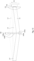
- Fig. 12 is a light path schematic of the light beam from the first laser chip 112a passing through the wedge structure 142a in Fig. 11 . Reference is made to Fig. 11 and Fig. 12 .
- the focusing lens 114 is omitted in Fig. 11 .
- Fig. 12 is a side view.
- the first laser chip 112a in the present embodiment is a semiconductor laser chip of three resonant cavities.
- the first laser chip 112a has a first resonant cavity 1122a, a third resonant cavity 1126a, and a second resonant cavity 1124a arranged along the first direction D1.
- the wedge structures 142a are similar to the wedge structures 142 in Fig. 6 , and the difference is that the wedge structures 142a further include second plane 1428a.
- the second plane 1428a connects the first inclined surface 1424a and the second inclined surface 1426a and is opposite to the first plane 1422a.
- the first inclined surface 1424a connects the second plane 1428a and have an angle ⁇ 2 therebetween.
- the second inclined surface 1426a connects the second plane 1428a and have an angle ⁇ 2 therebetween.
- the second plane 1428a faces the plano-convex lens 150 (see Fig. 3 ).
- the third resonant cavity 1126a emits a fourth light beam L4.
- the fourth light beam L4 passes through the second plane 1428a.
- the first light beam L1 and the second light beam L2 deflect and overlap each other when pass though the wedge structure 142a due to the angle ⁇ 2 and the index of refraction, and therefore another third light beam L3' formed.
- the first inclined surface 1424a of the wedge structure 142a is configured to refract the first light beam L1 along the first direction D1
- the second inclined surface 1426a is configured to refract the second light beam L2 along the reversed direction of the first direction D1.
- the second plane is parallel with the first plane 1422a.
- the traveling direction of the fourth light beam L4 is parallel with the direction of the optical axis A, and the fourth light beam L4 does not deflect after passing through the wedge structure 142a.
- a width W3 between the first resonant cavity 1122a and the second resonant cavity 1124a in the present embodiment is about 270 um.
- a width W4 of the openings of the first resonant cavity 1122a, the second resonant cavity 1124a, and the third resonant cavity 1126a is about 75 um, but the present disclosure are not limited thereto.
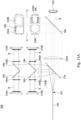
- Figs. 13A and 13B are schematics of laser light source module 300 according to another embodiment of the present disclosure.
- the light paths of the laser light source module 300 are omitted in Fig. 13B .
- the laser light source module 300 includes four first laser arrays 310A, 310B, 310C, 3100, four second laser arrays 320A, 320B, 320C, 320D, and one third laser array 330.
- the first laser arrays 310A ⁇ 310D are red semiconductor laser and have dual resonant cavities or multiple resonant cavities.
- the laser light source module 300 further includes four wedge arrays 340A, 340B, 340C, 340D, which respectively correspond to the four first laser arrays 310A ⁇ 310D.
- the wedge arrays 340A ⁇ 340D refract the light beams from the dual resonant cavities (or three resonant cavities) of the first laser arrays 310A ⁇ 310D and make them overlap each other.
- the laser light source module 300 further includes two plano-convex lenses 350A, 350B, an optical fiber 160, a first dichroic filter 370, a second dichroic filter 380, and multiple reflection mirrors 390.
- the blue lights B from the third laser array 330 are focused by the plano-convex lenses 350A.
- the red lights R from the first laser array 310A ⁇ 310D that passed through the wedge arrays 340A ⁇ 340D are focused by the plano-convex lenses 350B.
- the first dichroic filter 370 reflects the red lights R and enables transmittance of the blue lights B and the green lights G.
- the second dichroic filter 380 reflects the green lights G and enables transmittance of the blue lights B.
- the number of the third laser array 330 of the laser light source module 300 can less than the number of the first laser array 310A ⁇ 310D and less than the number of the second laser array 320A ⁇ 320D.
- the first laser chip 112 having multiple resonant cavities as shown in Fig. 6 are employed in the first laser array 310A ⁇ 310D to raise red laser light power. Accordingly, laser light power of different colors in the laser light source module 300 can be balanced.
- the laser light sources each can include a single laser chip or a single laser array, and the arrangement method is not limited.
- a single laser chip is accompanied with a single wedge structure, and the laser arrays are accompanied with the wedge array.
- the arrangement method is not limited.
- the first inclined surface and the second inclined surface of the wedge structure is configured to refract the light beams from the dual resonant cavities (or three resonant cavities) and make them overlap each other to form a single light beam.
- the light receiving range of the light receiving surface of the optical fiber can be reduced to cut production cost.
- the laser light source module be applied in a projection system having small light receiving area.
- the first laser array is a dual resonant cavities (or multiple resonant cavities) semiconductor laser, output power of the red laser is enhanced. Therefore, the light receiving efficiency for red light won't degrade when the light receiving surface reduces.
- the laser light source module can reduce light receiving area, cut production cost and remain the light receiving efficiency simultaneously.
Landscapes
- Physics & Mathematics (AREA)
- General Physics & Mathematics (AREA)
- Optics & Photonics (AREA)
- Condensed Matter Physics & Semiconductors (AREA)
- Electromagnetism (AREA)
- Semiconductor Lasers (AREA)
- Optical Couplings Of Light Guides (AREA)
Abstract
A laser light source module includes a laser chip, a wedge structure, a plano-convex lens, and an optical fiber. The laser chip is configured to emit a first light beam and a second light beam. The wedge structure is configured to refract the first light beam and the second light beam into a third light beam and make the first light beam and the second light beam overlap each other. The wedge structure is located between the laser chip and the plano-convex lens. The plano-convex lens is located between the wedge structure and the optical fiber.
Description
- The present invention relates to a laser light source module and projection apparatus.
- Common light sources of projector include UHP lamp, LED, laser phosphor, and pure laser. The pure laser has advantages such as long life-span, high brightness, and good color saturation. Due to the breakthrough of high power semiconductor laser technology, pure laser becomes a dominant laser light source.
- In RGB semiconductor laser technology, the red laser has lower power due to wavelength property and development level. If the number of red light source is increased for enhancing red laser output power, the optical design becomes complicated and the light receiving area becomes larger, which increases the production cost.
- Accordingly, it is still a development direction for the industry to provide a laser light source module that can solve the problems mentioned above.
- The invention provides a laser light source module.
- In one embodiment, the laser light source module includes a laser chip, a wedge structure, a plano-convex lens, and an optical fiber. The laser chip is configured to emit a first light beam and a second light beam. The wedge structure is configured to refract the first light beam and the second light beam into a third light beam and make the first light beam and the second light beam overlap each other. The wedge structure is located between the laser chip and the plano-convex lens. The plano-convex lens is located between the wedge structure and the optical fiber.
- In one embodiment, the laser chip is a red semiconductor laser chip of multiple resonant cavities.
- In one embodiment, the optical fiber includes a light receiving surface, the plano-convex lens is configured to focus the third light beam from the wedge structure to form a fifth light beam, and the light receiving surface is configured to receive the fifth light beam.
- In one embodiment, the laser chip includes a light-emitting surface, a first resonant cavity, and a second resonant cavity, the first resonant cavity emits the first light, the second resonant cavity emits the second light, the wedge structure includes a first plane, a first inclined surface, and a second inclined surface, the first plane faces the light-emitting surface of the laser chip, the first inclined surface and the second inclined surface face the plano-convex lens and are opposite to the first plane, and the first light beam and the second light beam pass through the first inclined surface and the second inclined surface, respectively.
- In one embodiment, the laser chip further includes a third resonant cavity located between the first resonant cavity and the second resonant cavity, the third resonant cavity emits a fourth light beam, the wedge structure includes a second plane, the second plane connects the first inclined surface and the second inclined surface and is opposite to the first plane, the fourth light beam passes through the second plane, and the first inclined surface and the second inclined surface of the wedge structure are configured to refract the first light beam and the second light beam towards the fourth light beam and make the first light beam and the second light beam to overlap each other.
- In one embodiment, a number of the at least one laser chip is plural, a number of the at least one wedge structure is plural, the wedge structures correspond to the laser chips respectively, the laser chips form at least one laser array, and the wedge structures form at least one wedge array.
- In one embodiment, the wedge structures of the wedge array are connected together.
- In one embodiment, each one of the laser chips includes the first resonant cavity and the second resonant cavity arranged along a first direction, the first inclined surfaces and the second inclined surfaces of the wedge structures are alternately arranged along the first direction, each one of the first inclined surfaces of the wedge structures is configured to refract more than one of the first light beams, and each one of the second inclined surfaces of the wedge structures is configured to refract more than one of the second light beams.
- In one embodiment, the first inclined surface and the second inclined surface of each one of the wedge structures have an angle therebetween, and the angles of the wedge structures are the same.
- Another aspect of the present disclosure is a projection apparatus.
- In one embodiment, the projection apparatus includes a laser light source module and a projection module. The projection module connects the laser light source module. The laser light source module includes a first laser chip, a second laser chip, a third laser chip, a wedge structure, and a plano-convex lens. The first laser chip is configured to emit a first light beam and a second light beam. The wedge structure is configured to refract the first light beam and the second light beam into a third light beam and make the first light beam and the second light beam overlap each other. The wedge structure is located between the first laser chip and the plano-convex lens.
- In one embodiment, the laser light source module further includes an optical fiber, and the plano-convex lens is located between the wedge structure and the optical fiber.
- In one embodiment, the first laser chip, the second laser chip, and the third laser chip are semiconductor lasers and are configured to emit laser lights with different wavelengths.
- In one embodiment, the first laser chip is a semiconductor laser chip of multiple resonant cavities, and the second laser chip and the third laser chip are semiconductor laser chips of single resonant cavity.
- In one embodiment, the first laser chip is a red semiconductor laser chip, and the first laser chip includes a light-emitting surface, a first resonant cavity, and a second resonant cavity, the first resonant cavity emits the first light beam, the second resonant cavity emits the second light beam, the wedge structure includes a first plane, a first inclined surface, and a second inclined surface, the first plane faces the light-emitting surface of the first laser chip, the first inclined surface and the second inclined surface face the plano-convex lens and are opposite to the first plane, and the first light beam and the second light beam pass through the first inclined surface and the second inclined surface, respectively.
- In one embodiment, the first laser chip further includes a third resonant cavity located between the first resonant cavity and the second resonant cavity, the third resonant cavity emits a fourth light beam, the wedge structure further includes a second plane, the second plane connects the first inclined surface and the second inclined surface and are opposite to the first plane, the fourth light beam passes through the second plane, and the first inclined surface and the second inclined surface of the wedge structure are configured to respectively refract the first light beam and the second light beam towards the fourth light beam and make the first light beam and the second light beam overlap each other.
- In one embodiment, a number of the at least one first laser chip is plural, a number of the at least one wedge structure is plural, the wedge structures correspond to the first laser chips respectively, the first laser chips form at least one laser array, and the wedge structures form at least one wedge array.
- In one embodiment, each one of the first laser chips includes the first resonant cavity and the second resonant cavity arranged along a first direction, the first inclined surfaces and the second inclined surfaces of the wedge structures are alternately arranged along the first direction, each one of the first inclined surfaces of the wedge structures are configured to refract more than one of the first light beams, and each one of the second inclined surfaces of the wedge structures are configured to refract more than one of the second light beams.
- In one embodiment, the first inclined surface and the second inclined surface of each one of the wedge structures have an angle therebetween, and the angles of the wedge structures are the same.
- In one embodiment, a number of the second laser chip is plural, the second laser chips form multiple second laser array, a number of the at least one third laser chip is plural, the third laser chips form a third laser array, the first laser chips are red semiconductor laser chips, the second laser chips are green semiconductor laser chips, and the third laser chips are blue semiconductor laser chips.
- In the aforesaid embodiments, the wedge structure is configured to refract the light beams from the dual resonant cavities (or multiple resonant cavities) and make them overlap each other to form a single light beam. As such, the light receiving range of the light receiving surface of the optical fiber can be reduced to cut production cost. Such design enables the laser light source module be applied in a projection system having small light receiving area. The laser light source module can reduce light receiving area, cut production cost and remain the light receiving efficiency simultaneously.
- The invention can be more fully understood by reading the following detailed description of the embodiment, with reference made to the accompanying drawings as follows:
-
Fig. 1 is a schematic of a projection apparatus according to one embodiment of the present disclosure. -
Fig. 2 is a schematic of the laser light source module inFig. 1 . -
Fig. 3 is a partial schematic of the laser light source module inFig. 2 . -
Fig. 4 is an enlarged view of the first laser array inFig. 3 . -
Fig. 5 is an enlarged view of the wedge array inFig. 3 . -
Fig. 6 is a schematic of the first laser chip and the wedge structure according to one embodiment of the present disclosure. -
Fig. 7 is a light path schematic of the light beam from the first laser chip passes through the wedge structure inFig. 6 . -
Figs. 8A and 8B are simulated images of the first light beam and the second light beam of the first laser chip. -
Figs. 9A and 9B are real images of the first light beam and the second light beam of the first laser chip. -
Fig. 10 is a light schematic of the first laser array inFig. 4 . -
Fig. 11 is a schematic of the first laser chip and the wedge structure according to another embodiment of the present disclosure. -
Fig. 12 is a light path schematic of the light beam from the first laser chip passing through the wedge structure inFig. 11 . -
Figs. 13A and13B are schematics of laser light source module according to another embodiment of the present disclosure. - Reference will now be made in detail to the present embodiments of the invention, examples of which are illustrated in the accompanying drawings. Wherever possible, the same reference numbers are used in the drawings and the description to refer to the same or like parts.
-
Fig. 1 is a schematic of aprojection apparatus 10 according to one embodiment of the present disclosure.Fig. 2 is a schematic of the laserlight source module 100 inFig. 1 . Reference is made toFig. 1 andFig. 2 simultaneously. Theprojection apparatus 10 includes a laserlight source module 100 and aprojection module 200. The laserlight source module 100 includes afirst laser array 110, asecond laser array 120, athird laser array 130, awedge array 140, a plano-convex lens 150, and anoptical fiber 160. The laserlight source module 100 connects theprojection module 200 through theoptical fiber 160 and to transmit light signal. - Reference is made to
Fig. 2 . In the present embodiment, the laserlight source module 100 is a semiconductor laser. Thefirst laser array 110 includes multiplefirst laser chips 112. Thesecond laser array 120 includes multiple second laser chips 122. Thethird laser array 130 includes multiple third laser chips 132. Thefirst laser chips 112, thesecond laser chips 122, and thethird laser chips 132 are configured to emit laser lights with different wavelengths. - In the present embodiment, the
first laser array 110 is a red semiconductor laser, thesecond laser array 120 is a green semiconductor laser, and thethird laser array 130 is a blue semiconductor laser. Thewedge array 140 is located between thefirst laser array 110 and the plano-convex lens 150. Thewedge array 140 is configured to refract a red light R from thefirst laser array 110 and is accompanied by the plano-convex lens 150 to make the multiple laser light beams from thefirst laser chip 112 overlap each other so as to shrink the light spot and increase the red light R receiving efficiency of theoptical fiber 160. As such, the output power of the red laser optical fiber is enhanced, and the power of the laserlight source module 100 of different wavelengths can be balanced. - The laser
light source module 100 further includes a firstdichroic filter 170 and a seconddichroic filter 180. The firstdichroic filter 170 is located between thesecond laser array 120 and thethird laser array 130. The firstdichroic filter 170 reflects the green light G from thesecond laser array 120, and enables the transmittance of the blue light B from thethird laser array 130. The seconddichroic filter 180 is located between thewedge array 140 and the plano-convex lens 150. The seconddichroic filter 180 reflects the green light G from thesecond laser array 120 and the blue light B from thethird laser array 130, and enables the transmittance the red light R which is from thefirst laser array 110 and been refracted by thewedge array 140. - In the embodiment sown in
Fig. 2 . The relative positions of thefirst laser array 110, thesecond laser array 120, thethird laser array 130, the firstdichroic filter 170, and the seconddichroic filter 180 are not limited as demonstrated herein, as long as the different laser lights can enter theoptical fiber 160. -
Fig. 3 is a partial schematic of the laserlight source module 100 inFig. 2 . In the present embodiment, thefirst laser array 110, thewedge array 140, the plano-convex lens 150, and theoptical fiber 160 are sequentially arranged along the direction of the optical axis A, but the present disclosure is not limited thereto. The plano-convex lens 150 is located between thewedge array 140 and theoptical fiber 160. Thefirst laser array 110 includes a light-emittingsurface 110S. The light-emittingsurface 110S faces thewedge array 140. In other words, a normal direction of the light-emittingsurface 110S is parallel with the direction of the optical axis A. In other embodiment, the normal direction of the light-emittingsurface 110S is not parallel with the direction of the optical axis A, and the light passed through thewedge array 140 can be transmit to the plano-convex lens 150 through other optical element. Theoptical fiber 160 has alight receiving surface 162. Thelight receiving surface 162 faces the plano-convex lens 150. -
Fig. 4 is an enlarged view of thefirst laser array 110 inFig. 3 . The multiplefirst laser chips 112 form afirst laser array 110 having seven rows and four columns, but the present disclosure is not limited thereto. The concrete structures of thefirst laser chip 112 will be described in the following paragraphs. As shown inFig. 3 andFig. 4 , thefirst laser array 110 has a focusinglens 114 facing thewedge array 140, and each one of thefirst laser chip 112 corresponds to a single focusinglens 114. There are 28 focusinglens 114 in this embodiment which collectively form a lens array of thefirst laser array 110. -
Fig. 5 is an enlarged view of thewedge array 140 inFig. 3 . Thewedge array 140 includes multiple wedge structures 142 (the region labeled by the dashed frame). Eachwedge structures 142 inFig. 5 correspond to eachfirst laser chips 112 inFig. 4 . Specifically, there are 28wedge structures 142 which form awedge array 140 having seven rows and four columns. - In the present embodiment, the
wedge structures 142 that are located at the same row are connected together. In other words, thewedge array 140 of the present embodiment can be considered as seven strip shape wedge structures each formed by fourwedge structures 142 at the same row, and then those seven strip shape wedge structures arranged along the first direction D1 are connected to form thewedge array 140. - For clarity, the embodiment having only one
first laser chip 112 accompanied with onewedge structure 142 will be described in detail firstly.Fig. 6 is a schematic of thefirst laser chip 112 and thewedge structure 142 according to one embodiment of the present disclosure.Fig. 7 is a light path schematic of the light beam from thefirst laser chip 112 passes through thewedge structure 142 inFig. 6 . Reference is made toFig. 6 andFig. 7 . The focusinglens 114 is omitted inFig. 6 , andFig. 7 is a side view. - The
first laser chip 112 is a semiconductor laser chip of dual resonant cavities (dual emitter). Thefirst laser chip 112 has a firstresonant cavity 1122 and a secondresonant cavity 1124 arranged along the first direction D1. The first direction D1 is perpendicular to the direction of optical axis A, and the first direction D1 is perpendicular to the normal direction of the light-emittingsurface 110S. In the present embodiment, for example, the first direction D1 is a vertical direction. In other embodiment, the firstresonant cavity 1122 and the secondresonant cavity 1124 can be arranged along the horizontal direction. - A width W1 between the first
resonant cavity 1122 and the secondresonant cavity 1124 of the present embodiment is about 270 um, and an opening width W2 of the firstresonant cavity 1122 and the secondresonant cavity 1124 is about 75 um, but the present disclosure is not limited thereto. - The
wedge structure 142 includes afirst plane 1422, a firstinclined surface 1424 and a secondinclined surface 1426. Thefirst plane 1422 faces the light-emittingsurface 110S of thefirst laser chip 112. The firstinclined surface 1424 and the secondinclined surface 1426 are opposite to thefirst plane 1422 and face the plano-convex lens 150 (seeFig. 3 ). The firstinclined surface 1424 and the secondinclined surface 1426 have an angle θ1 therebetween. - As shown in
Fig. 6 andFig. 7 , the firstresonant cavity 1122 emits the first light beam L1, and the secondresonant cavity 1124 emits the second light beam L2. The first light beam L1 and the second light beam L2 are red lights. The first light beam L1 and the second light beam L2 pass through the focusinglens 114 and travel towards thewedge structure 142. - The first light beam L1 and the second light beam L2 respectively pass through the first
inclined surface 1424 and the secondinclined surface 1426 after passing through thefirst plane 1422. Specifically, the first light beam L1 and the second light beam L2 deflect when pass though thewedge structure 142 due to the angle θ1 and the index of refraction. In the view potion inFig. 7 , the first light beam L1 deflects upward after passing through the firstinclined surface 1424, and the second light beam L2 deflects downwards after passing through the secondinclined surface 1426. In other words, the first light beam L1 deflects along the first direction D1 after passing through the firstinclined surface 1424, the second light beam L2 deflects along the reversed direction of the first direction D1 after passing through the secondinclined surface 1426. Accordingly, the firstinclined surface 1424 and the secondinclined surface 1426 are configured to refract the first light beam L1 and the second light beam L2 from thefirst laser chip 112 and makes them overlap each other to form a third light beam L3. - Material of the
wedge structures 142 can be arbitrary transparent material that can refract light such as glass. Size of thewedge structure 142 is determined based on the size of thefirst laser chip 112. The angle θ1 of thewedge structure 142 can be changed according to the index of refraction difference and the distance between thewedge structure 142 and adjacent elements. -
Figs. 8A and 8B are simulated images of the first light beam L1 and the second light beam L2 of thefirst laser chip 112. Simulated images of the first light beam L1 and the second light beam L2 without passing through thewedge structure 142 are illustrated inFig. 8A . The circular dashed line indicates alight receiving range 164 of thelight receiving surface 162 of theoptical fiber 160 that is necessary to receive the first light beam L1 and the second light beam L2. Simulated images of the first light beam L1 and the second light beam L2 after passing through thewedge structure 142 are illustrated inFig. 8B . The circular dashed line indicates alight receiving range 166 of thelight receiving surface 162 of theoptical fiber 160 that is necessary to receive the third light beam L3. - As shown in
Fig. 8A , the first light beam L1 and the second light beam L2 travel to thelight receiving surface 162 of theoptical fiber 160 and form two light spots. A length of these two light spots in the first direction D1 is in a range from about 0.9 mm to 1.0 mm, and the distance between the two light spots in the first direction D1 is about 1.0 mm. A diameter of thelight receiving range 164 of thelight receiving surface 162 of theoptical fiber 160 is about 2.9 mm. - As shown in
Fig. 8B , since the firstinclined surface 1424 and the secondinclined surface 1426 can refract the first light beam L1 and the second light beam L2 and makes them overlap each other to form the third light beam L3, single light spot is formed on thelight receiving surface 162 of theoptical fiber 160. A length of the light spot in the first direction D1 is smaller than about 1.6 mm. Therefore, a diameter of thelight receiving range 166 of thelight receiving surface 162 of theoptical fiber 160 can be reduced to about 1.6 mm. -
Figs. 9A and 9B are real images of the first light beam L1 and the second light beam L2 of thefirst laser chip 112. Real images of the first light beam L1 and the second light beam L2 without passing through thewedge structure 142 are illustrated inFig. 9A . The first light beam L1 and the second light beam L2 form two light spots. A distance between the two dashed lines inFig. 9A is about 3.6 mm. Real images of the third light beam L3 formed by the first light beam L1 and the second light beam L2 passed through thewedge structure 142 are illustrated inFig. 9B . The third light beam L3 form a single light spot. The distance between the two dashed lines inFig. 9B is reduced to about 1.6 mm. - According to
Fig. 8A to Fig. 9B , the firstinclined surface 1424 and the secondinclined surface 1426 can refract the light beams from the dual resonant cavities of a single laser chip and make the light beams overlap each other to form a single light beam. As such, thelight receiving range 166 of thelight receiving surface 162 of theoptical fiber 160 can be reduced to cut production cost. Such design enables the laserlight source module 100 be applied in a projection system having small light receiving area such as the systems using fused optical bundle or small entry integration rod. - In addition, since the
first laser array 110 is a semiconductor laser of dual resonant cavities (or multiple resonant cavities), output power of the red laser is enhanced. Therefore, the light receiving efficiency for red light won't degrade when thelight receiving surface 162 reduces. The laserlight source module 100 can reduce light receiving area, cut production cost and remain the light receiving efficiency simultaneously. - Reference is made to
Fig. 2 . In other embodiment, thesecond laser array 120 can include a singlesecond laser chip 122 which is a semiconductor laser chip of single resonant cavity. In other embodiments, thethird laser array 130 can include a singlethird laser chip 132 which is a semiconductor laser chip of single resonant cavity. In other words, configurations of the laser chips with different colors can be adjusted according to the required light emitting power. -
Fig. 10 is a light schematic of thefirst laser array 110 inFig. 4 . Reference is made toFig. 4 andFig. 10 simultaneously. The first laser chip 112 (the embodiment inFig. 6 ) having dual resonant cavities is applied to thefirst laser array 110 shown inFig. 4 . Two cross sections of the two light spots are acquired inFig. 10 , and the light spots are used to describe the light beams herein. - Each of the
first laser chips 112 of thefirst laser array 110 emits the first light beam L1 and the second light beam L2 arranged along the first direction D1. A distribution of the light spots in this embodiment has four columns and fourteen rows. The first light beam L1 and the second light beam L2 travel along the direction of the optical axis A, and the first light beam L1 and the second light beam L2 gradually expand and the sizes of the light spots gradually increase. - Reference is made to
Fig. 5 andFig. 10 . Thewedge structures 142 are repeatedly arranged along the first direction D1. There are seven rectangular firstinclined surfaces 1424 and seven rectangular secondinclined surfaces 1426 are alternately arranged along the first direction D1. In this embodiment, each one of the firstinclined surfaces 1424 of thewedge structures 142 are configured to refract four first light beams L1 at the same row, and each one of the secondinclined surfaces 1426 of thewedge structures 142 are configured to refract more four second light beams L2 at the same row. Therefore, 56 overlapped light beams from the first laser array 110 (28 first light beams L1 and 28 second light beams L2) by thewedge array 140 form 28 third light beams L3. Reference is made toFig. 3 , 28 third light beams L3 can be integrated as a single one fifth light beam L5 through the plano-convex lens 150 and enter theoptical fiber 160. - Reference is made to
Fig. 4 andFig. 5 simultaneously. The concrete structures of each one of thefirst laser chips 112 in this embodiment are substantially the same, and therefore the angles θ1 of the firstinclined surfaces 1424 and the secondinclined surfaces 1426 of each one of thewedge structures 142 are the same. In other words, the angles θ1 of thewedge structures 142 are not correlated with the positions of thewedge structure 142 relative to theoverall wedge array 140. - The angles θ1 of the
wedge structures 142 are correlated with the radius of curvature of the plano-convex lens 150. For example, in the embodiment shown inFig. 3 , the numerical aperture (NA) of theoptical fiber 160 is about 0.12. A maximum light receiving angle of theoptical fiber 160 can be derived through the equationNA = n sin θ, which is about +/-12.7 degrees. Assume that a distance between the plano-convex lens 150 and theoptical fiber 160 is about 113.4 mm, and a curvature of radius of the plano-convex lens 150 is about 85 mm derived from the equation
- The distance between the
wedge structure 142 and thefirst laser array 110 can be determined according to requirement or laser property. In this embodiment, the distance between thewedge structure 142 and thefirst laser array 110 is about 50 mm, and the distance between the plano-convex lens 150 and thewedge structure 142 is about 46 mm. Assumes that a distance between a center of the first light beam L1 and a center of the second light beam L2 is about 1.5 mm, the angle θ1 of thewedge structure 142 made with glass is about 1.8682 degrees through Snell's Law. - Accordingly, when the index of refraction of the
wedge structure 142 is fixed, the larger the angle θ1 of thewedge structure 142 is, the larger the defection angle between the first light beam and the second light beam are. Therefore, the distance between the overlapping position of the light spots and thewedge structure 142 becomes shorter. When the angle θ1 of thewedge structure 142 is fixed, the larger the index of refraction of thewedge structure 142 is, the larger the defection angle between the first light beam and the second light beam are. Therefore, the distance between the overlapping position of the light spots and thewedge structure 142 becomes shorter. - Reference is made to
Fig. 3 . It is noted that the 28 first light beams L1 inFig. 10 can be integrated as only one first light beam, and the 28 second light beams L2 can be integrated as only one second light beam when those light beams are merely focused by the plano-convex lens 150 without thewedge array 140. In other words, two separate light spots are formed when the lights are focused merely through the plano-convex lens 150. That is, the plano-convex lens 150 cannot make the light beams from the dual resonant cavities of the same laser chip overlap each other. Therefore, it is not sufficient to form a single light beam whose light spot is small enough to enter thelight receiving surface 162 of theoptical fiber 160 merely by using the plano-convex lens 150 as light focusing element. - In addition, if the positions of the plano-
convex lens 150 and thewedge array 140 are exchanges, the 28 first light beams L1 will be focused as a light beam having a greater light spot through the plano-convex lens 150 first, and the 28 second light beams L2 will be focused as another light beam having a greater light spot. These two light beams separate from each other. Under such condition, it works poorly to refract the light beam formed by the integrated 28 first light beams L1 by one firstinclined surface 1424 and to refract the light beam formed by the integrated 28 second light beams L2 by one secondinclined surface 1426. In other words, since each one of thewedge structures 142 in the present disclosure directly refract the first light beam L1 and the second light beam L2 from the dual resonant cavities of single one laser chip, the light spots can overlap each other and the light receiving efficiency is improved. -
Fig. 11 is a schematic of thefirst laser chip 112a and thewedge structure 142a according to another embodiment of the present disclosure.Fig. 12 is a light path schematic of the light beam from thefirst laser chip 112a passing through thewedge structure 142a inFig. 11 . Reference is made toFig. 11 andFig. 12 . The focusinglens 114 is omitted inFig. 11 .Fig. 12 is a side view. - The
first laser chip 112a in the present embodiment is a semiconductor laser chip of three resonant cavities. Thefirst laser chip 112a has a firstresonant cavity 1122a, a thirdresonant cavity 1126a, and a secondresonant cavity 1124a arranged along the first direction D1. - The
wedge structures 142a are similar to thewedge structures 142 inFig. 6 , and the difference is that thewedge structures 142a further includesecond plane 1428a. Thesecond plane 1428a connects the firstinclined surface 1424a and the secondinclined surface 1426a and is opposite to thefirst plane 1422a. The firstinclined surface 1424a connects thesecond plane 1428a and have an angle θ2 therebetween. The secondinclined surface 1426a connects thesecond plane 1428a and have an angle θ2 therebetween. Thesecond plane 1428a faces the plano-convex lens 150 (seeFig. 3 ). - As shown in
Fig. 11 andFig. 12 , the thirdresonant cavity 1126a emits a fourth light beam L4. The fourth light beam L4 passes through thesecond plane 1428a. The first light beam L1 and the second light beam L2 deflect and overlap each other when pass though thewedge structure 142a due to the angle θ2 and the index of refraction, and therefore another third light beam L3' formed. The firstinclined surface 1424a of thewedge structure 142a is configured to refract the first light beam L1 along the first direction D1, and the secondinclined surface 1426a is configured to refract the second light beam L2 along the reversed direction of the first direction D1. Specifically, the second plane is parallel with thefirst plane 1422a. The traveling direction of the fourth light beam L4 is parallel with the direction of the optical axis A, and the fourth light beam L4 does not deflect after passing through thewedge structure 142a. - A width W3 between the first
resonant cavity 1122a and the secondresonant cavity 1124a in the present embodiment is about 270 um. A width W4 of the openings of the firstresonant cavity 1122a, the secondresonant cavity 1124a, and the thirdresonant cavity 1126a is about 75 um, but the present disclosure are not limited thereto. -
Figs. 13A and13B are schematics of laserlight source module 300 according to another embodiment of the present disclosure. The light paths of the laserlight source module 300 are omitted inFig. 13B . In the present embodiment, the laserlight source module 300 includes fourfirst laser arrays second laser arrays third laser array 330. As described above, thefirst laser arrays 310A~310D are red semiconductor laser and have dual resonant cavities or multiple resonant cavities. The laserlight source module 300 further includes fourwedge arrays first laser arrays 310A~310D. Thewedge arrays 340A~340D refract the light beams from the dual resonant cavities (or three resonant cavities) of thefirst laser arrays 310A~310D and make them overlap each other. - The laser
light source module 300 further includes two plano-convex lenses optical fiber 160, a firstdichroic filter 370, a seconddichroic filter 380, and multiple reflection mirrors 390. The blue lights B from thethird laser array 330 are focused by the plano-convex lenses 350A. The red lights R from thefirst laser array 310A~310D that passed through thewedge arrays 340A~340D are focused by the plano-convex lenses 350B. The firstdichroic filter 370 reflects the red lights R and enables transmittance of the blue lights B and the green lights G. The seconddichroic filter 380 reflects the green lights G and enables transmittance of the blue lights B. - In general, blue laser chip has higher power due to better development level of the blue laser technique, and the red laser chip has lowest power. Therefore, the number of the
third laser array 330 of the laserlight source module 300 can less than the number of thefirst laser array 310A~310D and less than the number of thesecond laser array 320A~320D. Thefirst laser chip 112 having multiple resonant cavities as shown inFig. 6 are employed in thefirst laser array 310A~310D to raise red laser light power. Accordingly, laser light power of different colors in the laserlight source module 300 can be balanced. - According to the embodiments above, the laser light sources each can include a single laser chip or a single laser array, and the arrangement method is not limited. A single laser chip is accompanied with a single wedge structure, and the laser arrays are accompanied with the wedge array. The arrangement method is not limited.
- In summary, the first inclined surface and the second inclined surface of the wedge structure is configured to refract the light beams from the dual resonant cavities (or three resonant cavities) and make them overlap each other to form a single light beam. As such, the light receiving range of the light receiving surface of the optical fiber can be reduced to cut production cost. Such design enables the laser light source module be applied in a projection system having small light receiving area. In addition, since the first laser array is a dual resonant cavities (or multiple resonant cavities) semiconductor laser, output power of the red laser is enhanced. Therefore, the light receiving efficiency for red light won't degrade when the light receiving surface reduces. The laser light source module can reduce light receiving area, cut production cost and remain the light receiving efficiency simultaneously.
Claims (19)
- A laser light source module (100, 300), comprising:at least one laser chip (112, 112a, 122, 132) configured to emit a first light beam (L1) and a second light beam (L2);at least one wedge structure (142, 142a) configured to refract the first light beam (L1) and the second light beam (L2) and make the first light beam (L1) and the second light beam (L2) overlap each other to form a third light beam (L3);a plano-convex lens (150, 350A, 350B), wherein the wedge structure (142, 142a) is located between the laser chip (112, 112a, 122, 132) and the plano-convex lens (150, 350A, 350B); andan optical fiber (160), wherein the plano-convex lens (150, 350A, 350B) is located between the wedge structure (142, 142a) and the optical fiber (160).
- The laser light source module of claim 1, wherein the laser chip (112, 112a, 122, 132) is a red semiconductor laser chip of multiple resonant cavities.
- The laser light source module of one of the claims 1-2, wherein the optical fiber (160) comprises a light receiving surface (162), the plano-convex lens (150, 350A, 350B) is configured to focus the third light beam (L3) from the wedge structure (142, 142a) to form a fifth light beam (L5), and the light receiving surface (162) is configured to receive the fifth light beam (L5).
- The laser light source module of one of the claims 1-3, wherein the laser chip (112, 112a, 122, 132) comprises a light-emitting surface (110S), a first resonant cavity (1122, 1122a), and a second resonant cavity (1124, 1124a), the first resonant cavity (1122, 1122a) emits the first light beam (L1), the second resonant cavity (1124, 1124a) emits the second light beam (L2), the wedge structure (142, 142a) comprises a first plane (1422, 1422a), a first inclined surface (1424, 1424a), and a second inclined surface (1426, 1426a), the first plane (1422, 1422a) faces the light-emitting surface (110S) of the laser chip (112, 112a, 122, 132), the first inclined surface (1424, 1424a) and the second inclined surface (1426, 1426a) face the plano-convex lens (150, 350A, 350B) and are opposite to the first plane (1422, 1422a), and the first light beam (L1) and the second light beam (L2) pass through the first inclined surface (1424, 1424a) and the second inclined surface (1426, 1426a), respectively.
- The laser light source module of claim 4, wherein the laser chip (112, 112a, 122, 132) further comprises a third resonant cavity (1126a) located between the first resonant cavity (1122, 1122a) and the second resonant cavity (1124, 1124a), the third resonant cavity (1126a) emits a fourth light beam (L4), the wedge structure (142, 142a) comprises a second plane (1428a), the second plane (1428a) connects the first inclined surface (1424, 1424a) and the second inclined surface (1426, 1426a) and is opposite to the first plane (1422, 1422a), the fourth light beam (L4) passes through the second plane (1428a), and the first inclined surface (1424, 1424a) and the second inclined surface (1426, 1426a) of the wedge structure (142, 142a) are configured to refract the first light beam (L1) and the second light beam (L2) towards the fourth light beam (L4) and make the first light beam (L1) and the second light beam (L2) to overlap each other.
- The laser light source module of one of the claims 4-5, wherein a number of the at least one laser chip (112, 112a, 122, 132) is plural, a number of the at least one wedge structure (142, 142a) is plural, the wedge structures (142, 142a) correspond to the laser chips (112, 112a, 122, 132) respectively, the laser chips (112, 112a, 122, 132) form at least one laser array (110, 120, 130, 310A~310D, 320A~320D, 330), and the wedge structures (142, 142a) form at least one wedge array (140, 340A-340D).
- The laser light source module of claim 6, wherein the wedge structures (142, 142a) of the wedge array (140, 340A-340D) are connected together.
- The laser light source module of one of the claims 6-7, wherein each one of the laser chips (112, 112a, 122, 132) comprises the first resonant cavity (1122, 1122a) and the second resonant cavity (1124, 1124a) arranged along a first direction (D1), the first inclined surfaces (1424, 1424a) and the second inclined surfaces (1426, 1426a) of the wedge structures (142, 142a) are alternately arranged along the first direction (D1), each one of the first inclined surfaces (1424, 1424a) of the wedge structures (142, 142a) is configured to refract more than one of the first light beams (L1), and each one of the second inclined surfaces (1426, 1426a) of the wedge structures (142, 142a) is configured to refract more than one of the second light beams (L2).
- The laser light source module of claim 8, wherein the first inclined surface (1424, 1424a) and the second inclined surface (1426, 1426a) of each one of the wedge structures (142, 142a) have an angle (θ1) therebetween, and the angles (θ1) of the wedge structures (142, 142a) are the same.
- A projection apparatus (10), comprising:a laser light source module (100, 300), comprising:at least one first laser chip (112, 112a), at least one second laser chip (122), and at least one third laser chip (132), wherein the first laser chip (112, 112a) is configured to emit a first light beam (L1) and a second light beam (L2);at least one wedge structure (142, 142a) configured to refract the first light beam (L1) and the second light beam (L2) into a third light beam (L3) and make the first light beam (L1) and the second light beam (L2) overlap each other; anda plano-convex lens (150, 350A, 350B), wherein the wedge structure (142, 142a) is located between the first laser chip (112, 112a) and the plano-convex lens (150, 350A, 350B); anda projection module (200) connecting the laser light source module (100).
- The projection apparatus of claim 10, wherein the laser light source module (100) further comprises an optical fiber (160), and the plano-convex lens (150, 350A, 350B) is located between the wedge structure (142, 142a) and the optical fiber (160).
- The projection apparatus of one of the claims 10-11, wherein the first laser chip (112, 112a), the second laser chip (122), and the third laser chip (132) are semiconductor lasers and are configured to emit laser lights with different wavelengths.
- The projection apparatus of one of the claims 10-12, wherein the first laser chip (112, 112a) is a semiconductor laser chip of multiple resonant cavities, and the second laser chip (122) and the third laser chip (132) are semiconductor laser chips of single resonant cavity.
- The projection apparatus of one of the claims 10-13, wherein the first laser chip (112, 112a) is a red semiconductor laser chip, and the first laser chip (112, 112a) comprises a light-emitting surface (110S), a first resonant cavity (1122, 1122a), and a second resonant cavity (1124, 1124a), the first resonant cavity (1122, 1122a) emits the first light beam (L1), the second resonant cavity (1124, 1124a) emits the second light beam (L2), the wedge structure (142, 142a) comprises a first plane (1422, 1422a), a first inclined surface (1424, 1424a), and a second inclined surface (1426, 1426a), the first plane (1422, 1422a) faces the light-emitting surface (110S) of the first laser chip (112, 112a), the first inclined surface (1424, 1424a) and the second inclined surface (1426, 1426a) face the plano-convex lens (150, 350A, 350B) and are opposite to the first plane (1422, 1422a), and the first light beam (L1) and the second light beam (L2) pass through the first inclined surface (1424, 1424a) and the second inclined surface (1426, 1426a), respectively.
- The projection apparatus of claim 14, wherein the first laser chip (112, 112a) further comprises a third resonant cavity (1126a) located between the first resonant cavity (1122, 1122a) and the second resonant cavity (1124, 1124a), the third resonant cavity (1126a) emits a fourth light beam (L4), the wedge structure (142, 142a) further comprises a second plane (1428a), the second plane (1428a) connects the first inclined surface (1424, 1424a) and the second inclined surface (1426, 1426a) and are opposite to the first plane (1422, 1422a), the fourth light beam (L4) passes through the second plane (1428a), and the first inclined surface (1424, 1424a) and the second inclined surface (1426, 1426a) of the wedge structure (142, 142a) are configured to respectively refract the first light beam (L1) and the second light beam (L2) towards the fourth light beam (L4) and make the first light beam (L1) and the second light beam (L2) overlap each other.
- The projection apparatus of one of the claims 14-15, wherein a number of the at least one first laser chip (112, 112a) is plural, a number of the at least one wedge structure (142, 142a) is plural, the wedge structures (142, 142a) correspond to the first laser chips (112, 112a) respectively, the first laser chips (112, 112a) form at least one laser array (110, 310A~310D), and the wedge structures (142, 142a) form at least one wedge array (140, 340A-340D).
- The projection apparatus of claim 16, wherein each one of the first laser chips (112, 112a) comprises the first resonant cavity (1122, 1122a) and the second resonant cavity (1124, 1124a) arranged along a first direction (D1), the first inclined surfaces (1424,1424a) and the second inclined surfaces (1426, 1426a) of the wedge structures (142, 142a) are alternately arranged along the first direction (D1), each one of the first inclined surfaces (1424,1424a) of the wedge structures (142, 142a) are configured to refract more than one of the first light beams (L1), and each one of the second inclined surfaces (1426, 1426a) of the wedge structures (142, 142a) are configured to refract more than one of the second light beams (L2).
- The projection apparatus of claim 17, wherein the first inclined surface (1424,1424a) and the second inclined surface (1426, 1426a) of each one of the wedge structures (142, 142a) have an angle (θ1) therebetween, and the angles (θ1) of the wedge structures (142, 142a) are the same.
- The projection apparatus of one of the claims 17-18, wherein a number of the second laser chip (122) is plural, the second laser chips (122) form a plurality of second laser array (120, 320A~320D), a number of the at least one third laser chip (132) is plural, the third laser chips (132) form a third laser array (130, 330), the first laser chips (112, 112a) are red semiconductor laser chips, the second laser chips (122) are green semiconductor laser chips, and the third laser chips (132) are blue semiconductor laser chips.
Applications Claiming Priority (1)
| Application Number | Priority Date | Filing Date | Title |
|---|---|---|---|
| CN202310916695.7A CN119376170A (en) | 2023-07-25 | 2023-07-25 | Laser light source module and projection device having the same |
Publications (1)
| Publication Number | Publication Date |
|---|---|
| EP4498537A1 true EP4498537A1 (en) | 2025-01-29 |
Family
ID=89897099
Family Applications (1)
| Application Number | Title | Priority Date | Filing Date |
|---|---|---|---|
| EP24156479.8A Pending EP4498537A1 (en) | 2023-07-25 | 2024-02-08 | Laser light source module and projection apparatus having the same |
Country Status (3)
| Country | Link |
|---|---|
| US (1) | US20250036015A1 (en) |
| EP (1) | EP4498537A1 (en) |
| CN (1) | CN119376170A (en) |
Citations (4)
| Publication number | Priority date | Publication date | Assignee | Title |
|---|---|---|---|---|
| US20150316234A1 (en) * | 2013-01-24 | 2015-11-05 | Panasonic Intellectual Property Management Co., Ltd. | Light source, light source unit, and light source module using same |
| US20160029001A1 (en) * | 2012-04-13 | 2016-01-28 | Red.Com, Inc. | Video projector system |
| US20210285619A1 (en) * | 2018-12-06 | 2021-09-16 | Nuvoton Technology Corporation Japan | Light source unit, illumination device, processing equipment, and deflection element |
| US20230121969A1 (en) * | 2021-10-19 | 2023-04-20 | Nichia Corporation | Light source device |
-
2023
- 2023-07-25 CN CN202310916695.7A patent/CN119376170A/en active Pending
- 2023-11-27 US US18/519,161 patent/US20250036015A1/en active Pending
-
2024
- 2024-02-08 EP EP24156479.8A patent/EP4498537A1/en active Pending
Patent Citations (4)
| Publication number | Priority date | Publication date | Assignee | Title |
|---|---|---|---|---|
| US20160029001A1 (en) * | 2012-04-13 | 2016-01-28 | Red.Com, Inc. | Video projector system |
| US20150316234A1 (en) * | 2013-01-24 | 2015-11-05 | Panasonic Intellectual Property Management Co., Ltd. | Light source, light source unit, and light source module using same |
| US20210285619A1 (en) * | 2018-12-06 | 2021-09-16 | Nuvoton Technology Corporation Japan | Light source unit, illumination device, processing equipment, and deflection element |
| US20230121969A1 (en) * | 2021-10-19 | 2023-04-20 | Nichia Corporation | Light source device |
Also Published As
| Publication number | Publication date |
|---|---|
| CN119376170A (en) | 2025-01-28 |
| US20250036015A1 (en) | 2025-01-30 |
Similar Documents
| Publication | Publication Date | Title |
|---|---|---|
| US7988340B2 (en) | Prism sheet and backlight module | |
| JP7119986B2 (en) | projector | |
| CN101799589A (en) | Color separation optical element and image panel device | |
| US20090161076A1 (en) | Projection apparatus | |
| KR100739720B1 (en) | Color filter-free liquid crystal display device | |
| KR100453040B1 (en) | Collimating lens, collimating system and image displaying apparatus employing the same | |
| EP3690494B1 (en) | Lens array and lighting optical system | |
| US11089274B2 (en) | Light source device and projection apparatus | |
| US6796662B2 (en) | Illumination optical system and projector | |
| KR20180086225A (en) | Head-up display device and production method thereof | |
| KR20210116273A (en) | Micro lens system for a motor vehicle headlamp | |
| US20250036015A1 (en) | Laser light source module and projection apparatus having the same | |
| US9188730B2 (en) | Light source module using laser as light source | |
| US7699502B2 (en) | Optical member and lighting device having the same | |
| JP2025038147A (en) | Light Emitting Module | |
| TWI864904B (en) | Laser light source module and projection apparatus having the same | |
| CN112413428A (en) | a light source system | |
| US20230121969A1 (en) | Light source device | |
| JP2002318364A (en) | Lighting equipment | |
| CN214064607U (en) | Light source system | |
| US6928198B2 (en) | Exposure head | |
| JP2022146623A (en) | Inspection device | |
| US12571518B2 (en) | Light source device | |
| JP7615276B1 (en) | Light-emitting module and front-illuminated liquid crystal on silicon module | |
| KR20190052352A (en) | RGB laser module system for implementating white beam |
Legal Events
| Date | Code | Title | Description |
|---|---|---|---|
| PUAI | Public reference made under article 153(3) epc to a published international application that has entered the european phase |
Free format text: ORIGINAL CODE: 0009012 |
|
| STAA | Information on the status of an ep patent application or granted ep patent |
Free format text: STATUS: THE APPLICATION HAS BEEN PUBLISHED |
|
| AK | Designated contracting states |
Kind code of ref document: A1 Designated state(s): AL AT BE BG CH CY CZ DE DK EE ES FI FR GB GR HR HU IE IS IT LI LT LU LV MC ME MK MT NL NO PL PT RO RS SE SI SK SM TR |
|
| STAA | Information on the status of an ep patent application or granted ep patent |
Free format text: STATUS: REQUEST FOR EXAMINATION WAS MADE |
|
| 17P | Request for examination filed |
Effective date: 20250416 |