EP4498155A2 - Elektronische vorrichtung - Google Patents
Elektronische vorrichtung Download PDFInfo
- Publication number
- EP4498155A2 EP4498155A2 EP24219268.0A EP24219268A EP4498155A2 EP 4498155 A2 EP4498155 A2 EP 4498155A2 EP 24219268 A EP24219268 A EP 24219268A EP 4498155 A2 EP4498155 A2 EP 4498155A2
- Authority
- EP
- European Patent Office
- Prior art keywords
- light
- light conversion
- light emitting
- backlight module
- optical patterns
- Prior art date
- Legal status (The legal status is an assumption and is not a legal conclusion. Google has not performed a legal analysis and makes no representation as to the accuracy of the status listed.)
- Pending
Links
Images







Classifications
-
- G—PHYSICS
- G02—OPTICS
- G02B—OPTICAL ELEMENTS, SYSTEMS OR APPARATUS
- G02B6/00—Light guides; Structural details of arrangements comprising light guides and other optical elements, e.g. couplings
- G02B6/0001—Light guides; Structural details of arrangements comprising light guides and other optical elements, e.g. couplings specially adapted for lighting devices or systems
- G02B6/0011—Light guides; Structural details of arrangements comprising light guides and other optical elements, e.g. couplings specially adapted for lighting devices or systems the light guides being planar or of plate-like form
- G02B6/0066—Light guides; Structural details of arrangements comprising light guides and other optical elements, e.g. couplings specially adapted for lighting devices or systems the light guides being planar or of plate-like form characterised by the light source being coupled to the light guide
-
- G—PHYSICS
- G02—OPTICS
- G02F—OPTICAL DEVICES OR ARRANGEMENTS FOR THE CONTROL OF LIGHT BY MODIFICATION OF THE OPTICAL PROPERTIES OF THE MEDIA OF THE ELEMENTS INVOLVED THEREIN; NON-LINEAR OPTICS; FREQUENCY-CHANGING OF LIGHT; OPTICAL LOGIC ELEMENTS; OPTICAL ANALOGUE/DIGITAL CONVERTERS
- G02F1/00—Devices or arrangements for the control of the intensity, colour, phase, polarisation or direction of light arriving from an independent light source, e.g. switching, gating or modulating; Non-linear optics
- G02F1/01—Devices or arrangements for the control of the intensity, colour, phase, polarisation or direction of light arriving from an independent light source, e.g. switching, gating or modulating; Non-linear optics for the control of the intensity, phase, polarisation or colour
- G02F1/13—Devices or arrangements for the control of the intensity, colour, phase, polarisation or direction of light arriving from an independent light source, e.g. switching, gating or modulating; Non-linear optics for the control of the intensity, phase, polarisation or colour based on liquid crystals, e.g. single liquid crystal display cells
- G02F1/133—Constructional arrangements; Operation of liquid crystal cells; Circuit arrangements
- G02F1/1333—Constructional arrangements; Manufacturing methods
- G02F1/1335—Structural association of cells with optical devices, e.g. polarisers or reflectors
- G02F1/1336—Illuminating devices
- G02F1/133614—Illuminating devices using photoluminescence, e.g. phosphors illuminated by UV or blue light
-
- G—PHYSICS
- G02—OPTICS
- G02B—OPTICAL ELEMENTS, SYSTEMS OR APPARATUS
- G02B6/00—Light guides; Structural details of arrangements comprising light guides and other optical elements, e.g. couplings
- G02B6/0001—Light guides; Structural details of arrangements comprising light guides and other optical elements, e.g. couplings specially adapted for lighting devices or systems
- G02B6/0011—Light guides; Structural details of arrangements comprising light guides and other optical elements, e.g. couplings specially adapted for lighting devices or systems the light guides being planar or of plate-like form
- G02B6/0033—Means for improving the coupling-out of light from the light guide
- G02B6/005—Means for improving the coupling-out of light from the light guide provided by one optical element, or plurality thereof, placed on the light output side of the light guide
-
- G—PHYSICS
- G02—OPTICS
- G02B—OPTICAL ELEMENTS, SYSTEMS OR APPARATUS
- G02B6/00—Light guides; Structural details of arrangements comprising light guides and other optical elements, e.g. couplings
- G02B6/0001—Light guides; Structural details of arrangements comprising light guides and other optical elements, e.g. couplings specially adapted for lighting devices or systems
- G02B6/0011—Light guides; Structural details of arrangements comprising light guides and other optical elements, e.g. couplings specially adapted for lighting devices or systems the light guides being planar or of plate-like form
- G02B6/0033—Means for improving the coupling-out of light from the light guide
- G02B6/005—Means for improving the coupling-out of light from the light guide provided by one optical element, or plurality thereof, placed on the light output side of the light guide
- G02B6/0055—Reflecting element, sheet or layer
-
- G—PHYSICS
- G02—OPTICS
- G02B—OPTICAL ELEMENTS, SYSTEMS OR APPARATUS
- G02B6/00—Light guides; Structural details of arrangements comprising light guides and other optical elements, e.g. couplings
- G02B6/0001—Light guides; Structural details of arrangements comprising light guides and other optical elements, e.g. couplings specially adapted for lighting devices or systems
- G02B6/0011—Light guides; Structural details of arrangements comprising light guides and other optical elements, e.g. couplings specially adapted for lighting devices or systems the light guides being planar or of plate-like form
- G02B6/0033—Means for improving the coupling-out of light from the light guide
- G02B6/0058—Means for improving the coupling-out of light from the light guide varying in density, size, shape or depth along the light guide
-
- G—PHYSICS
- G02—OPTICS
- G02B—OPTICAL ELEMENTS, SYSTEMS OR APPARATUS
- G02B6/00—Light guides; Structural details of arrangements comprising light guides and other optical elements, e.g. couplings
- G02B6/0001—Light guides; Structural details of arrangements comprising light guides and other optical elements, e.g. couplings specially adapted for lighting devices or systems
- G02B6/0011—Light guides; Structural details of arrangements comprising light guides and other optical elements, e.g. couplings specially adapted for lighting devices or systems the light guides being planar or of plate-like form
- G02B6/0066—Light guides; Structural details of arrangements comprising light guides and other optical elements, e.g. couplings specially adapted for lighting devices or systems the light guides being planar or of plate-like form characterised by the light source being coupled to the light guide
- G02B6/0068—Arrangements of plural sources, e.g. multi-colour light sources
-
- G—PHYSICS
- G02—OPTICS
- G02B—OPTICAL ELEMENTS, SYSTEMS OR APPARATUS
- G02B6/00—Light guides; Structural details of arrangements comprising light guides and other optical elements, e.g. couplings
- G02B6/0001—Light guides; Structural details of arrangements comprising light guides and other optical elements, e.g. couplings specially adapted for lighting devices or systems
- G02B6/0011—Light guides; Structural details of arrangements comprising light guides and other optical elements, e.g. couplings specially adapted for lighting devices or systems the light guides being planar or of plate-like form
- G02B6/0081—Mechanical or electrical aspects of the light guide and light source in the lighting device peculiar to the adaptation to planar light guides, e.g. concerning packaging
- G02B6/0086—Positioning aspects
- G02B6/0088—Positioning aspects of the light guide or other optical sheets in the package
-
- G—PHYSICS
- G02—OPTICS
- G02F—OPTICAL DEVICES OR ARRANGEMENTS FOR THE CONTROL OF LIGHT BY MODIFICATION OF THE OPTICAL PROPERTIES OF THE MEDIA OF THE ELEMENTS INVOLVED THEREIN; NON-LINEAR OPTICS; FREQUENCY-CHANGING OF LIGHT; OPTICAL LOGIC ELEMENTS; OPTICAL ANALOGUE/DIGITAL CONVERTERS
- G02F1/00—Devices or arrangements for the control of the intensity, colour, phase, polarisation or direction of light arriving from an independent light source, e.g. switching, gating or modulating; Non-linear optics
- G02F1/01—Devices or arrangements for the control of the intensity, colour, phase, polarisation or direction of light arriving from an independent light source, e.g. switching, gating or modulating; Non-linear optics for the control of the intensity, phase, polarisation or colour
- G02F1/13—Devices or arrangements for the control of the intensity, colour, phase, polarisation or direction of light arriving from an independent light source, e.g. switching, gating or modulating; Non-linear optics for the control of the intensity, phase, polarisation or colour based on liquid crystals, e.g. single liquid crystal display cells
- G02F1/133—Constructional arrangements; Operation of liquid crystal cells; Circuit arrangements
- G02F1/1333—Constructional arrangements; Manufacturing methods
- G02F1/1335—Structural association of cells with optical devices, e.g. polarisers or reflectors
- G02F1/1336—Illuminating devices
- G02F1/133602—Direct backlight
- G02F1/133603—Direct backlight with LEDs
-
- G—PHYSICS
- G02—OPTICS
- G02F—OPTICAL DEVICES OR ARRANGEMENTS FOR THE CONTROL OF LIGHT BY MODIFICATION OF THE OPTICAL PROPERTIES OF THE MEDIA OF THE ELEMENTS INVOLVED THEREIN; NON-LINEAR OPTICS; FREQUENCY-CHANGING OF LIGHT; OPTICAL LOGIC ELEMENTS; OPTICAL ANALOGUE/DIGITAL CONVERTERS
- G02F1/00—Devices or arrangements for the control of the intensity, colour, phase, polarisation or direction of light arriving from an independent light source, e.g. switching, gating or modulating; Non-linear optics
- G02F1/01—Devices or arrangements for the control of the intensity, colour, phase, polarisation or direction of light arriving from an independent light source, e.g. switching, gating or modulating; Non-linear optics for the control of the intensity, phase, polarisation or colour
- G02F1/13—Devices or arrangements for the control of the intensity, colour, phase, polarisation or direction of light arriving from an independent light source, e.g. switching, gating or modulating; Non-linear optics for the control of the intensity, phase, polarisation or colour based on liquid crystals, e.g. single liquid crystal display cells
- G02F1/133—Constructional arrangements; Operation of liquid crystal cells; Circuit arrangements
- G02F1/1333—Constructional arrangements; Manufacturing methods
- G02F1/1335—Structural association of cells with optical devices, e.g. polarisers or reflectors
- G02F1/1336—Illuminating devices
- G02F1/133602—Direct backlight
- G02F1/133605—Direct backlight including specially adapted reflectors
-
- G—PHYSICS
- G02—OPTICS
- G02F—OPTICAL DEVICES OR ARRANGEMENTS FOR THE CONTROL OF LIGHT BY MODIFICATION OF THE OPTICAL PROPERTIES OF THE MEDIA OF THE ELEMENTS INVOLVED THEREIN; NON-LINEAR OPTICS; FREQUENCY-CHANGING OF LIGHT; OPTICAL LOGIC ELEMENTS; OPTICAL ANALOGUE/DIGITAL CONVERTERS
- G02F1/00—Devices or arrangements for the control of the intensity, colour, phase, polarisation or direction of light arriving from an independent light source, e.g. switching, gating or modulating; Non-linear optics
- G02F1/01—Devices or arrangements for the control of the intensity, colour, phase, polarisation or direction of light arriving from an independent light source, e.g. switching, gating or modulating; Non-linear optics for the control of the intensity, phase, polarisation or colour
- G02F1/13—Devices or arrangements for the control of the intensity, colour, phase, polarisation or direction of light arriving from an independent light source, e.g. switching, gating or modulating; Non-linear optics for the control of the intensity, phase, polarisation or colour based on liquid crystals, e.g. single liquid crystal display cells
- G02F1/133—Constructional arrangements; Operation of liquid crystal cells; Circuit arrangements
- G02F1/1333—Constructional arrangements; Manufacturing methods
- G02F1/1335—Structural association of cells with optical devices, e.g. polarisers or reflectors
- G02F1/1336—Illuminating devices
- G02F1/133602—Direct backlight
- G02F1/133606—Direct backlight including a specially adapted diffusing, scattering or light controlling members
-
- G—PHYSICS
- G02—OPTICS
- G02F—OPTICAL DEVICES OR ARRANGEMENTS FOR THE CONTROL OF LIGHT BY MODIFICATION OF THE OPTICAL PROPERTIES OF THE MEDIA OF THE ELEMENTS INVOLVED THEREIN; NON-LINEAR OPTICS; FREQUENCY-CHANGING OF LIGHT; OPTICAL LOGIC ELEMENTS; OPTICAL ANALOGUE/DIGITAL CONVERTERS
- G02F1/00—Devices or arrangements for the control of the intensity, colour, phase, polarisation or direction of light arriving from an independent light source, e.g. switching, gating or modulating; Non-linear optics
- G02F1/01—Devices or arrangements for the control of the intensity, colour, phase, polarisation or direction of light arriving from an independent light source, e.g. switching, gating or modulating; Non-linear optics for the control of the intensity, phase, polarisation or colour
- G02F1/13—Devices or arrangements for the control of the intensity, colour, phase, polarisation or direction of light arriving from an independent light source, e.g. switching, gating or modulating; Non-linear optics for the control of the intensity, phase, polarisation or colour based on liquid crystals, e.g. single liquid crystal display cells
- G02F1/133—Constructional arrangements; Operation of liquid crystal cells; Circuit arrangements
- G02F1/1333—Constructional arrangements; Manufacturing methods
- G02F1/1335—Structural association of cells with optical devices, e.g. polarisers or reflectors
- G02F1/1336—Illuminating devices
- G02F1/133602—Direct backlight
- G02F1/133606—Direct backlight including a specially adapted diffusing, scattering or light controlling members
- G02F1/133607—Direct backlight including a specially adapted diffusing, scattering or light controlling members the light controlling member including light directing or refracting elements, e.g. prisms or lenses
-
- G—PHYSICS
- G02—OPTICS
- G02F—OPTICAL DEVICES OR ARRANGEMENTS FOR THE CONTROL OF LIGHT BY MODIFICATION OF THE OPTICAL PROPERTIES OF THE MEDIA OF THE ELEMENTS INVOLVED THEREIN; NON-LINEAR OPTICS; FREQUENCY-CHANGING OF LIGHT; OPTICAL LOGIC ELEMENTS; OPTICAL ANALOGUE/DIGITAL CONVERTERS
- G02F1/00—Devices or arrangements for the control of the intensity, colour, phase, polarisation or direction of light arriving from an independent light source, e.g. switching, gating or modulating; Non-linear optics
- G02F1/01—Devices or arrangements for the control of the intensity, colour, phase, polarisation or direction of light arriving from an independent light source, e.g. switching, gating or modulating; Non-linear optics for the control of the intensity, phase, polarisation or colour
- G02F1/13—Devices or arrangements for the control of the intensity, colour, phase, polarisation or direction of light arriving from an independent light source, e.g. switching, gating or modulating; Non-linear optics for the control of the intensity, phase, polarisation or colour based on liquid crystals, e.g. single liquid crystal display cells
- G02F1/133—Constructional arrangements; Operation of liquid crystal cells; Circuit arrangements
- G02F1/1333—Constructional arrangements; Manufacturing methods
- G02F1/1335—Structural association of cells with optical devices, e.g. polarisers or reflectors
- G02F1/1336—Illuminating devices
- G02F1/133602—Direct backlight
- G02F1/133609—Direct backlight including means for improving the color mixing, e.g. white
Definitions
- the disclosure relates to a module and a device, and more particularly to a backlight module and an electronic device.
- a backlight module in an electronic device uses a blue light emitting unit with a light conversion layer to generate white light.
- a blue light emitting unit with a light conversion layer to generate white light.
- an edge region of the backlight module is prone to white light color point shift, which results in inconsistent white light performance in the center region and in the edge region of the backlight module.
- the disclosure provides a backlight module and an electronic device, which help address the problem of white light color point shift in an edge region of a backlight module.
- the backlight module has a main region and a peripheral region near the main region.
- the backlight module includes a light conversion layer, multiple light conversion patterns, and multiple light emitting units.
- the light conversion patterns are located in the peripheral region.
- the light emitting units emit a light beam.
- a first portion of the light beam emitted from the main region has at least one corresponding position in a CIE 1931 color space.
- a second portion of the light beam emitted from the peripheral region has at least one corresponding position in the CIE 1931 color space.
- One among the at least one corresponding position of the first portion of the light beam has corresponding coordinates (x1, y1).
- One among the at least one corresponding position of the second portion of the light beam has corresponding coordinates (x2, y2).
- the corresponding coordinates (x1, y1) and the corresponding coordinates (x2, y2) satisfy the following relation: 0 ⁇
- the electronic device includes the backlight module and a display panel disposed on the backlight module.
- terms concerning attachments and connections such as “connected,” “interconnected,” and the like, unless defined otherwise, mean two structures directly contact each other, or mean the two structures do not directly contact each other and other structures are disposed therebetween.
- the terms concerning attachments and connections may also include a relationship in which the two structures are both movable or fixed.
- the terms “electrically connected to” and “coupled to” include any direct and indirect electrical connection means.
- the terms such as “first” and “second” mentioned in the specification or the claims are only used to name different elements or to distinguish different embodiments or scopes, and are not intended to limit the upper or lower limit of the number of the elements, nor are they intended to limit the manufacturing order or disposition order of the elements.
- an electronic device may include, but not limited to, a display device, an antenna device, a sensing device, a light emitting device, or a splicing device.
- the electronic device may be a bendable electronic device or a flexible electronic device.
- the electronic device may include, for example, a liquid crystal layer or a light emitting diode (LED).
- the light emitting diode may include, for example but not limited to, an organic light emitting diode (OLED), a mini light emitting diode (mini LED), a micro light emitting diode (micro LED), or a quantum dot light emitting diode (QLED or QDLED), fluorescence, phosphors, other suitable materials, or a combination of the above, but the disclosure is not limited thereto.
- OLED organic light emitting diode
- mini LED mini light emitting diode
- micro LED micro light emitting diode
- QLED or QDLED quantum dot light emitting diode
- fluorescence phosphors
- phosphors other suitable materials
- the display device of the disclosure may be a non-self-luminous display device, such as a liquid crystal display device, but the disclosure is not limited thereto.
- a liquid crystal display device such as a liquid crystal display device
- the liquid crystal display device is used as the display device to describe the disclosure, but the disclosure is not limited thereto.
- FIG. 1 is a schematic cross-sectional view of an electronic device according to an embodiment of the disclosure.
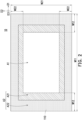
- FIG. 2 is a schematic top view of a backlight module in FIG. 1 .
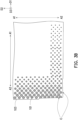
- FIG. 3A and FIG. 3B are the first partial schematic top views of different regions of a reflecting layer on which multiple light conversion patterns are disposed.
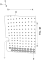
- FIG. 4A and FIG. 4B are the second partial schematic top views of different regions of the reflecting layer on which multiple light conversion patterns are disposed.
- FIG. 5A and FIG. 5B are the third partial schematic top views of different regions of the reflecting layer on which multiple light conversion patterns are disposed.
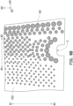
- FIG. 6A and FIG. 6B are the fourth partial schematic top views of different regions of the reflecting layer on which multiple light conversion patterns are disposed.
- FIG. 7B are the fifth partial schematic top views of different regions of the reflecting layer on which multiple light conversion patterns are disposed.
- FIG. 8 is a schematic cross-sectional view of an electronic device according to another embodiment of the disclosure.
- FIG. 9 is a partially enlarged schematic view of a backlight module in FIG. 8 .
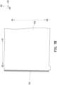
- FIG. 10 is a partial schematic top view of a backlight module according to an embodiment of the disclosure.
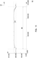
- FIG. 11 is a schematic cross-sectional view of the light conversion pattern.
- an electronic device 1 may include, but not limited to, a backlight module 10 and a display panel 12 disposed on the backlight module 10. According to different requirements, the electronic device 1 may further include one or more elements or film layers, and details thereof are not repeated herein.
- the backlight module 10 has a main region A1 and a peripheral region A2 near the main region A1.
- the peripheral region A2 is near the main region A1 and may surround the main region A1 and be connected to the main region A1, but the disclosure is not limited thereto.
- the maximum width of the peripheral region A2 in a direction may be 10% of the maximum width of the backlight module 10 in the same direction.
- a maximum width W12 of a side (e.g., the left side) of the peripheral region A2 in a first direction D1 may be 10% of a maximum width W11 of the backlight module 10 in the first direction D1.
- the maximum width W12 of another side (e.g., the right side) of the peripheral region A2 in the first direction D1 may be 10% of the maximum width W11 of the backlight module 10 in the first direction D1
- a maximum width W22 of a side (e.g., the upper side) of the peripheral region A2 in a second direction D2 may be 10% of a maximum width W21 of the backlight module 10 in the second direction D2.
- the maximum width W22 of another side (e.g., the lower side) of the peripheral region A2 in the second direction D2 may be 10% of the maximum width W21 of the backlight module 10 in the second direction D2.
- the second direction D2 and the first direction D1 are different.
- the second direction D2 may be perpendicular to the first direction D1.
- the backlight module 10 may include, but not limited to, a light conversion layer 100, multiple light conversion patterns 101, and multiple light emitting units 102 (only one schematically shown in FIG. 1 ). According to different requirements, the backlight module 10 may further include one or more elements or film layers.
- the backlight module 10 may include, but not limited to, a reflecting layer 103, a light guide element 104, an optical film sheet 105, an optical film sheet 106, a circuit board 107, an adhesive layer 108, a backing plate 109, and a plastic frame 110.
- the maximum width W11 of the backlight module 10 in the first direction D1 refers to the maximum distance between two opposite outer edges of the plastic frame 110 in the first direction D1
- the maximum width W21 of the backlight module 10 in the second direction D2 refers to the maximum distance between the two opposite outer edges of the plastic frame 110 in the second direction D2.
- the maximum width W11 of the backlight module 10 in the first direction D1 refers to the maximum distance between two opposite outer edges of the backing plate 109 in the first direction D1
- the maximum width W21 of the backlight module 10 in the second direction D2 refers to the maximum distance between the two opposite outer edges of the backing plate 109 in the second direction D2. It should be understood that the maximum width W12 and the maximum width W22 of the peripheral region A2 may be the same or different.
- the peripheral region A2 may include a first region A21 and a second region A22.
- the first region A21 is located between the main region A1 and the second region A22.
- the second region A22 may be defined by the plastic frame 110.
- the second region A22 is substantially the same as where the plastic frame 110 is located when viewed in the normal direction of the backlight module 10 (e.g., a third direction D3 perpendicular to the first direction D1 and the second direction D2).
- the second region A22 is substantially the same as the region between the edge of the light conversion pattern 101 adjacent to the backing plate 109 and the outer edge of the backing plate 109 when viewed, for example, in the third direction D3.
- the light conversion layer 100 may include a mono-layer or multi-layer structure. In some embodiments, the light conversion layer 100 is disposed between the optical film sheet 105 and the light guide element 104, but the disclosure is not limited thereto. For example, when the light conversion layer 100 is irradiated by a short-wavelength light beam, at least a portion of the short-wavelength light beam (e.g., blue light) may be converted into a long-wavelength light beam (e.g., red light, green light, or yellow light, etc.), but the disclosure is not limited thereto.
- a short-wavelength light beam e.g., blue light
- a long-wavelength light beam e.g., red light, green light, or yellow light, etc.
- the material of the light conversion layer 100 may include, but not limited to, fluorescence, phosphorescence, quantum dots (QD), other suitable materials, or a combination of at least two of the foregoing.
- the light conversion layer 100 may be formed on a film before fixed on the light guide element 104, or may be directly coated on the light guide element 104.
- the light conversion layer 100 may be disposed between the light emitting element 102 and the light guide element 104, or may be disposed in the light guide element 104, but the disclosure is not limited thereto.
- the light conversion patterns 101 may be located in the peripheral region A2. In some embodiments, the light conversion patterns 101 are disposed on the reflecting layer 103 and are located between the light guide element 104 and the reflecting layer 103. In some embodiments, a portion of the light conversion pattern 101 may be located in the main region A1 and near the peripheral region A2. For example, the light conversion patterns 101, when irradiated by a short-wavelength light beam, may convert at least a portion of the short-wavelength light beam (e.g., blue light) into a long-wavelength light beam (e.g., red light, green light, yellow light, or blue light of wavelength longer than the incident light/incident light beam, etc.), but the disclosure is not limited thereto. In some embodiments, the material of the light conversion patterns 101 may include, but not limited to, fluorescence, phosphorescence, quantum dots, other suitable materials, or a combination of at least two of the foregoing.
- the light emitting units 102 are located in the peripheral region A2. Taking an edge-type backlight module as an example, the light emitting units 102 may be disposed near a lateral surface S1 of the light guide element 104. In another embodiment, the light emitting units 102 may be disposed near the lateral surface S1 and a lateral surface S1' of the light guide element 104 opposite to each other, but the disclosure is not limited thereto.
- the light emitting units 102 may be disposed on the circuit board 107 and be electrically connected to the circuit board 107.
- the light emitting units 102 may include the aforementioned light emitting diode, and details thereof are not repeated herein.
- the light emitting units 102 can emit a light beam B.
- the light emitting units 102 may be blue light emitting diodes, and the light beam B is blue.
- a portion of the light beam B (blue light) from the light emitting units 102 may be converted into yellow light by the light conversion patterns 101 or the light conversion layer 100, while a portion of the light beam B (blue light) not converted by the light conversion patterns 101 or the light conversion layer 100 may be mixed with the yellow light after conversion to form white light.
- a portion of the light beam B from the light emitting units 102 enters the light guide element 104 through the lateral surface S1 of the light guide element 104, and is transmitted in the light guide element 104 from the peripheral region A2 toward the main region A1 by total internal reflection.
- Microstructures (not shown) or mesh points (not shown) disposed on a bottom surface S2 of the light guide element 104 can destroy total internal reflection, such that a portion of the light beam B can be transmitted through a top surface S3 of the light guide element 104 out of the light guide element 104.
- the portion of the light beam B transmitted out of the light guide element 104 may be converted into yellow light by the light conversion layer 100, and the yellow light after conversion may be mixed with a portion of blue light in the light beam B transmitted out of the light guide element 104 to form white light.
- another portion of the light beam B from the light emitting units 102 e.g., a light beam with a large angle
- the portion of the light beam B (blue light) not converted by the light conversion patterns 101 may be mixed with the yellow light after conversion to form white light.
- the reflecting layer 103 is disposed on the backing plate 109 and between the bottom surface S2 of the light guide element 104 and the backing plate 109.
- the reflecting layer 103 may reflect the light beam B transmitted away from the display panel 12, which may improve the light utilization rate of the backlight module 10.
- the reflecting layer 103 may include a white reflecting sheet, a white tape, or a metal reflecting sheet; alternatively, the reflecting layer 103 may be disposed on the backing plate 109 through a coating process, but the disclosure is not limited thereto.
- the reflecting layer 103 may be further disposed between the lateral surface S 1' of the light guide element 104 away from the light emitting element 102 and the backing plate 109 to improve the light utilization rate of the backlight module 10.
- the light guide element 104 is disposed between the reflecting layer 103 and the light conversion layer 100.
- at least one of the bottom surface S2 and the top surface S3 of the light guide element 104 may be formed with multiple microstructures (not shown) or multiple mesh points (not shown).
- the material of the light guide element 104 may include, but not limited to, plastic, glass, or the like.
- the optical film sheet 105 and the optical film sheet 106 are disposed on the light conversion layer 100 and are located between the display panel 12 and the light conversion layer 100.
- the optical film sheet 105 and the optical film sheet 106 may respectively be a diffuser sheet and a prism sheet, but the disclosure is not limited thereto.
- the backlight module 10 may include, but not limited to, one or more diffuser sheets, one or more prism sheets, and/or one or more other optical film sheets.
- the circuit board 107 may be attached on the side wall of the backing plate 109 through the adhesive layer 108, such that the light emitting units 102 face the lateral surface S1 of the light guide element 104.
- the circuit board 107 may include a printed circuit board, and the adhesive layer 108 may include, but not limited to, a tape or an optical adhesive.
- the plastic frame 110 may be disposed on the backing plate 109 and carry the display panel 12. A portion of the plastic frame 110 may be disposed on the outer side of the side wall of the backing plate 109, and an accommodating space may be formed between the plastic frame 110 and the backing plate 109, which may allow the light guide element 104, the light conversion layer 100, the optical film sheet 105, and the optical film sheet 106 to be accommodated in the accommodating space between the plastic frame 110 and the backing plate 109. In some embodiments, the plastic frame 110 may be disposed on the backing plate 109 and carry the display panel 12, the optical film sheet 105, and the optical film sheet 106.
- a portion of the plastic frame 110 may be disposed on the outer side of the side wall of the backing plate 109, and an accommodating space may be formed between the plastic frame 110 and the backing plate 109, which may allow the light guide element 104 and the light conversion layer 100 to be accommodated in the accommodating space.
- the optical film 105 and the optical film sheet 106 may be disposed between the plastic frame 110 and the display panel 12.
- the plastic frame 110 may be made of an opaque material to shield the elements thereunder.
- the backing plate 109 may carry the display panel 12, and an accommodating space may be formed between the display panel 12 and the backing plate 109, which may allow the light guide element 104, the light conversion layer 100, the optical film sheet 105, and the optical film sheet 106 to be accommodated in the accommodating space.
- the display panel 12 may be disposed above the optical film sheet 106 through the plastic frame 110.
- the display panel 12 may include, but not limited to, a non-self-luminous display panel, such as a liquid crystal display panel.
- the light beam B may form white light after passing through the light conversion layer 100.
- the white light passes through the optical film sheet 105 and the optical film sheet 106 in sequence and may serve as the light source of the display panel 12.
- a first portion light beam P1 emitted from the main region A1 has at least one corresponding position (chromaticity point) in the CIE 1931 color space.
- a second portion light beam P2 emitted from the peripheral region A2 has at least one corresponding position (chromaticity point) in the CIE 1931 color space.
- One among the at least one corresponding position of the first portion light beam P1 of the light beam B has corresponding coordinates (x1, y1).
- One among the at least one corresponding position of the second portion light beam P2 of the light beam B has corresponding coordinates (x2, y2).
- the corresponding coordinates (x1, y1) and the corresponding coordinates (x2, y2) may satisfy the following relation: 0 ⁇
- the corresponding coordinates (x1, y1) and the corresponding coordinates (x2, y2) may further satisfy the following relation: 0 ⁇
- the light conversion patterns 101 disposed near one or more edges of the backlight module 10 may convert blue light into yellow light.
- the blue light and the yellow light are mixed to form white light, thereby addressing the problem of white light color point shift in the peripheral region A2.
- white light performance in the main region A1 and that in the peripheral region A2 of the backlight module 10 become consistent and then satisfy 0 ⁇
- the corresponding coordinates (x1, y1) and the corresponding coordinates (x2, y2) may further satisfy the following relation: 0 ⁇
- the corresponding coordinates (x1, y1) and the corresponding coordinates (x2, y2) may further satisfy the following relation: 0 ⁇
- Table 1 Display panels in three different sizes are listed in Table 1 below as examples, but it should be understood that Table 1 is only for exemplification and not for limiting the disclosure.
- the corresponding coordinates (x1, y1) are, for example, a chromaticity point of any place within the range of 12% to 15% of the distance from the edge of the backlight module in the main region of the backlight module.
- the corresponding coordinates (x2, y2) are, for example, a chromaticity point of any place within the peripheral region of the backlight module near the main region.
- the light conversion patterns help make the white light performance in the main region and that in the peripheral region of the backlight module to become consistent.
- Table 1 screen size 49 inches 55 inches 65 inches x1 0.260 ⁇ 0.270 0.260 ⁇ 0.272 0.260 ⁇ 0.275 y1 0.230 ⁇ 0.240 0.230 ⁇ 0.245 0.230 ⁇ 0.243 x2 0.270 ⁇ 0.296 0.272 ⁇ 0.293 0.270 ⁇ 0.280 y2 0.255 ⁇ 0.280 0.240 ⁇ 0.276 0.240 ⁇ 0.253
- the shape of the light conversion pattern 101 may be similar to a circle or an ellipse when viewed from the top, but the disclosure is not limited thereto.
- the light conversion patterns 101 may include a first light conversion pattern 101-1 and a second light conversion pattern 101-2.
- the first light conversion pattern 101-1 is closer to the main region A1 than the second light conversion pattern 101-2.
- the light emitting units are arranged along the second direction D2, and a dotted line L1 may be shown in the top view, starting from any place in the main region A1 to the peripheral region A2 and being perpendicular to the second direction D2 (e.g., parallel to the first direction D1).
- the light conversion pattern 101 closest to the main region A1 on this dotted line L1 serves as the first light conversion pattern 101-1
- the light conversion pattern farthest from the main region A1 on this dotted line L1 serves as the second light conversion pattern 101-2.
- the first light conversion pattern 101-1 and the second light conversion pattern 101-2 may have different widths. For example, a maximum width W101-1 (the maximum width in the first direction D1) of the first light conversion pattern 101-1 may be less than a maximum width W101-2 (the maximum width in the first direction D1) of the second light conversion pattern 101-2).
- the maximum width of the light conversion patterns 101 near the peripheral region A2 may be greater than the maximum width of the light conversion patterns 101 near the main region A1, such that blue light near the periphery region A2 can be more converted into yellow light to address the problem of white light color point shift.
- the top view shows a dotted line L2 starting from any place in the main region A1 to the peripheral region A2 and being parallel to the second direction D2.
- the light conversion patterns on this dotted line L2 may substantially have the same maximum width, but the disclosure is not limited thereto.
- the light conversion patterns 101 may be arranged alternately.
- an included angle between a direction in which any light conversion pattern 101 and the nearest light conversion pattern 101 are arranged and a direction perpendicular to the arrangement direction of the light emitting units (e.g., the first direction D1) is not equal to 0 degrees or 90 degrees.
- the included angle between an arrangement direction D4 (or an arrangement direction D5) of the second light conversion pattern 101-2 and a light conversion pattern 101-3 (or a light conversion pattern 101-4) and the first direction D1 is not equal to 0 degrees or 90 degrees.
- the probability of blue light being converted into yellow light may be increased, and the problem of white light color point shift may thus be addressed.
- the reflecting layer 103 may be cut to facilitate the assembly of the reflecting layer 103 and the backing plate 109. With this structure, as shown in FIG. 3A to FIG. 6B , the reflecting layer 103 has an edge C. In some embodiments, the light conversion patterns 101 disposed on the reflecting layer 103 may be cut as shown in FIG. 3A and FIG. 3B . In some embodiments, the light conversion patterns 101 disposed on the reflecting layer 103 may not be cut as shown in FIG. 4A and FIG. 4B . In some embodiments, the light conversion patterns 101 may be disposed on three edges of the reflecting layer 103, and one edge of the reflecting layer 103 is not disposed with any light conversion pattern as shown in FIG. 5A , FIG. 5B , FIG. 6A , and FIG. 6B . In some embodiments, one or all of the light conversion patterns 101 may be strip-shaped as shown in FIG. 7A and FIG. 7B .
- an electronic device 1A may include a backlight module 10A and the display panel 12.
- the main difference between the backlight module 10A and the backlight module 10 in FIG. 1 is that the backlight module 10A is a direct-type backlight module.
- the backlight module 10A may include, but not limited to, the light conversion layer 100, the light conversion patterns 101, the light emitting units 102, the reflecting layer 103, the optical film sheet 105, the optical film sheet 106, the backing plate 109, the plastic frame 110, and an optical film sheet 111.
- the light emitting units 102 may be disposed on the reflecting layer 103, and the reflecting layer 103 may be composed of, but not limited to, the uppermost metal layer of a circuit board or a layer with reflection (e.g., white paint).
- the reflecting layer 103 may further extend onto the side wall of the backing plate 109, and the light converting patterns 101 may be disposed on the reflecting layer 103 corresponding to the side wall of the backing plate 109.
- the light conversion patterns 101 may be arranged into a matrix, and in another embodiment, the light conversion patterns 101 may also be arranged alternately, but the disclosure is not limited thereto.
- One or more light conversion patterns 101 disposed near the backlight module 10A may convert a portion of blue light into yellow light, and the unconverted blue light may be mixed with the yellow light to form white light, thereby addressing the problem of white light color point shift in the peripheral region A2.
- white light performance in the main region A1 and that in the peripheral region A2 of the backlight module 10 become consistent and then satisfy 0 ⁇
- the light conversion patterns 101 may have the same size (e.g., width), but the disclosure is not limited thereto.
- a gap G between two adjacent ones among the light conversion patterns 101 may be greater than 0 and be less than or equal to half of a distance D between two adjacent ones among the light emitting units 102.
- the gap G may be the minimum distance between two adjacent light conversion patterns 101 among the light conversion patterns 101 in the row closest to the light emitting units 102 in the arrangement direction of the light emitting units 102 (e.g., the first direction D1).
- the distance D refers to the minimum distance between two same sides of two adjacent light emitting units 102 in the first direction D1 (e.g., from the left side of one to the left side of the other, from the right side of one to the right side of the other, or from the middle of one to the middle of the other of the two adjacent light emitting units 102 as shown in FIG. 10 ).
- the conversion of the light beam B emitted by the light emitting units 102 into yellow light may be improved, the white light performance between two adjacent light emitting units 102 and in front of the light emitting units 102 may be improved, or the problem of uneven brightness of the backlight module 10 may be addressed.
- the gap G of 0 means that the light conversion pattern adopts the strip pattern design as shown in FIG. 7A and FIG. 7B .
- the strip light conversion pattern may be disposed on the edge of the reflecting layer near the light incident side, but the disclosure is not limited thereto. In other embodiments, the strip light conversion pattern may also be disposed on multiple (e.g., two, three, or four) edges of the reflecting layer. Table 2 screen size 27 inches 49 inches 55 inches 65 inches gap G (mm) 0 2.6 2.6 3.8
- the cross-sectional shape of the light conversion pattern 101 may be substantially semi-elliptical and have a curved surface, but the disclosure is not limited thereto.
- the light conversion pattern 101 may be formed on the reflecting layer (not shown in FIG. 11 ) by printing, spray coating, or the like.
- a maximum thickness TH of the light conversion pattern 101 in the third direction D3 is, for example, less than or equal to a bottom width WB of the light conversion pattern 101 (e.g., the maximum width in the first direction D1).
- the light conversion pattern 101 can generate a relatively even light pattern.
- TH/WB may fall within the range of 0.01 to 1.0, which means 0.01 ⁇ TH/WB ⁇ 1.0.
- Table 3 Two screen sizes are listed in Table 3 below as examples, but it should be understood that Table 3 is only for exemplification and not for limiting the disclosure.
- the sizes of the light conversion patterns e.g., the bottom widths
- the bottom width of the third light conversion pattern is greater than the bottom width of the second light conversion pattern
- the bottom width of the second light conversion pattern is greater than the bottom width of the first light conversion pattern.
- TH/WB ⁇ 0.1 the maximum thickness TH of the light conversion pattern is too small, and this may increase the probability of blue light leakage from the edge region and cause chromatic aberration to occur.
- one or more light conversion patterns disposed near the backlight module convert a portion of blue light into yellow light, and the unconverted blue light may be mixed with the yellow light to form white light, thereby addressing the problem of white light color point shift in the peripheral region and making white light performance in the main region and that in the peripheral region of the backlight module become consistent.
- the width of the light conversion patterns near the peripheral region may be greater than the width of the light conversion patterns near the main region, such that the blue light near the peripheral region can be more converted into yellow light to address the problem of white light color point shift.
- the probability for blue light to be converted into yellow light may be increased to address the problem of white light color point shift.
- the light conversion patterns designed to have gaps therebetween may improve the white light performance between two adjacent light emitting units and in front of the light emitting units, or may address the problem of uneven brightness of the backlight module 10.
- chromatic aberration may be addressed by designing the cross-sectional shape of the light conversion pattern.
Landscapes
- Physics & Mathematics (AREA)
- Nonlinear Science (AREA)
- General Physics & Mathematics (AREA)
- Optics & Photonics (AREA)
- Mathematical Physics (AREA)
- Chemical & Material Sciences (AREA)
- Crystallography & Structural Chemistry (AREA)
- Planar Illumination Modules (AREA)
- Liquid Crystal (AREA)
Applications Claiming Priority (2)
| Application Number | Priority Date | Filing Date | Title |
|---|---|---|---|
| CN202110858430.7A CN115685619B (zh) | 2021-07-28 | 2021-07-28 | 背光模块以及电子装置 |
| EP22180914.8A EP4124905A1 (de) | 2021-07-28 | 2022-06-24 | Elektronische vorrichtung |
Related Parent Applications (1)
| Application Number | Title | Priority Date | Filing Date |
|---|---|---|---|
| EP22180914.8A Division EP4124905A1 (de) | 2021-07-28 | 2022-06-24 | Elektronische vorrichtung |
Publications (2)
| Publication Number | Publication Date |
|---|---|
| EP4498155A2 true EP4498155A2 (de) | 2025-01-29 |
| EP4498155A3 EP4498155A3 (de) | 2025-04-09 |
Family
ID=82308186
Family Applications (2)
| Application Number | Title | Priority Date | Filing Date |
|---|---|---|---|
| EP22180914.8A Withdrawn EP4124905A1 (de) | 2021-07-28 | 2022-06-24 | Elektronische vorrichtung |
| EP24219268.0A Pending EP4498155A3 (de) | 2021-07-28 | 2022-06-24 | Elektronische vorrichtung |
Family Applications Before (1)
| Application Number | Title | Priority Date | Filing Date |
|---|---|---|---|
| EP22180914.8A Withdrawn EP4124905A1 (de) | 2021-07-28 | 2022-06-24 | Elektronische vorrichtung |
Country Status (5)
| Country | Link |
|---|---|
| US (4) | US11656400B2 (de) |
| EP (2) | EP4124905A1 (de) |
| CN (3) | CN118483848A (de) |
| PH (1) | PH12022050298A1 (de) |
| TW (1) | TWI803252B (de) |
Families Citing this family (3)
| Publication number | Priority date | Publication date | Assignee | Title |
|---|---|---|---|---|
| CN118483848A (zh) * | 2021-07-28 | 2024-08-13 | 群创光电股份有限公司 | 发光装置 |
| KR102650104B1 (ko) * | 2022-03-22 | 2024-03-20 | 엘지전자 주식회사 | 디스플레이 디바이스 |
| CN221101211U (zh) * | 2023-09-26 | 2024-06-07 | 烟台富华达精密电子有限公司 | 背光模组和显示装置 |
Family Cites Families (25)
| Publication number | Priority date | Publication date | Assignee | Title |
|---|---|---|---|---|
| JP2006163425A (ja) * | 2004-05-12 | 2006-06-22 | Seiko Epson Corp | 表示装置および電子機器 |
| TW200600919A (en) * | 2004-06-22 | 2006-01-01 | Samsung Electronics Co Ltd | Optical film, backlight assembly and liquid crystal display device having the same |
| KR101035502B1 (ko) * | 2004-11-16 | 2011-05-20 | 엘지디스플레이 주식회사 | 발광다이오드를 이용한 액정표시장치모듈 |
| KR100638874B1 (ko) * | 2005-07-06 | 2006-10-27 | 삼성전기주식회사 | Led 광원이 도광판에 삽입된 백라이트 장치의광원-도광판 구조 및 이를 포함하는 백라이트 장치 |
| KR100613839B1 (ko) * | 2005-11-29 | 2006-08-17 | 주식회사 엘지에스 | 백라이트 유닛 |
| US7507012B2 (en) * | 2007-05-16 | 2009-03-24 | Rohm And Haas Denmark Finance A/S | LCD displays with light redirection |
| GB2461689A (en) * | 2008-07-07 | 2010-01-13 | Sharp Kk | Illumination panel for display back light |
| CN202521397U (zh) * | 2012-02-15 | 2012-11-07 | 青岛海信电器股份有限公司 | 背光模组 |
| CN103032765A (zh) * | 2012-12-11 | 2013-04-10 | 京东方科技集团股份有限公司 | 一种光源模组、液晶显示装置以及霓虹灯显示装置 |
| KR102203950B1 (ko) * | 2014-02-05 | 2021-01-19 | 삼성디스플레이 주식회사 | 광원 모듈, 이를 포함하는 백라이트 어셈블리 및 표시 장치 |
| US9535206B2 (en) | 2014-06-09 | 2017-01-03 | Apple Inc. | Display with structures for reducing blue edge effects |
| JP6576173B2 (ja) * | 2014-09-10 | 2019-09-18 | シチズン電子株式会社 | 面状ライトユニット、led素子及び導光板 |
| KR101572165B1 (ko) | 2014-12-09 | 2015-11-26 | 삼성전자 주식회사 | 디스플레이 장치 및 이에 포함되는 백 라이트 유닛 |
| KR20160116792A (ko) | 2015-03-31 | 2016-10-10 | 삼성전자주식회사 | 디스플레이 장치 |
| CN105864723A (zh) * | 2016-03-31 | 2016-08-17 | 纳晶科技股份有限公司 | 量子点膜、包含其的背光模组与显示设备 |
| CN109937323B (zh) * | 2016-11-07 | 2022-06-24 | 富士胶片株式会社 | 含光吸收体膜及背光单元 |
| US10937992B2 (en) * | 2017-10-30 | 2021-03-02 | Gio Optoelectronics Corp. | Light emitting device, manufacturing method thereof and display device using the same |
| CN208041696U (zh) | 2018-04-16 | 2018-11-02 | 京东方科技集团股份有限公司 | 背光源、背光模组和显示装置 |
| TWI878222B (zh) * | 2018-05-14 | 2025-04-01 | 晶元光電股份有限公司 | 一種發光裝置及其製造方法 |
| TWI661251B (zh) * | 2018-06-12 | 2019-06-01 | 友達光電股份有限公司 | 背光模組 |
| US11428988B2 (en) * | 2018-08-31 | 2022-08-30 | Nanosys, Inc. | Increasing color gamut performance and efficiency in quantum dot color conversion layers |
| TWI716158B (zh) * | 2018-10-22 | 2021-01-11 | 優美特創新材料股份有限公司 | 光轉換層、背光模組及包括其的顯示裝置 |
| CN111812885A (zh) * | 2019-04-10 | 2020-10-23 | 展晶科技(深圳)有限公司 | 光学透镜、背光模组和显示装置 |
| CN110780376B (zh) * | 2019-11-22 | 2021-10-26 | 京东方科技集团股份有限公司 | 导光板及其制作方法、背光源、显示装置和撞点设备 |
| CN118483848A (zh) * | 2021-07-28 | 2024-08-13 | 群创光电股份有限公司 | 发光装置 |
-
2021
- 2021-07-28 CN CN202410755710.9A patent/CN118483848A/zh active Pending
- 2021-07-28 CN CN202511027816.8A patent/CN120595514A/zh active Pending
- 2021-07-28 CN CN202110858430.7A patent/CN115685619B/zh active Active
-
2022
- 2022-03-23 TW TW111110829A patent/TWI803252B/zh active
- 2022-06-21 US US17/844,751 patent/US11656400B2/en active Active
- 2022-06-24 EP EP22180914.8A patent/EP4124905A1/de not_active Withdrawn
- 2022-06-24 EP EP24219268.0A patent/EP4498155A3/de active Pending
- 2022-06-30 PH PH1/2022/050298A patent/PH12022050298A1/en unknown
-
2023
- 2023-04-12 US US18/299,066 patent/US11867940B2/en active Active
- 2023-11-20 US US18/513,652 patent/US12153246B2/en active Active
-
2024
- 2024-10-24 US US18/926,288 patent/US20250044497A1/en active Pending
Also Published As
| Publication number | Publication date |
|---|---|
| TW202305282A (zh) | 2023-02-01 |
| US20250044497A1 (en) | 2025-02-06 |
| CN120595514A (zh) | 2025-09-05 |
| EP4498155A3 (de) | 2025-04-09 |
| US20230039599A1 (en) | 2023-02-09 |
| CN115685619B (zh) | 2025-08-12 |
| US11656400B2 (en) | 2023-05-23 |
| EP4124905A1 (de) | 2023-02-01 |
| PH12022050298A1 (en) | 2023-03-27 |
| US11867940B2 (en) | 2024-01-09 |
| CN115685619A (zh) | 2023-02-03 |
| US12153246B2 (en) | 2024-11-26 |
| US20240085615A1 (en) | 2024-03-14 |
| CN118483848A (zh) | 2024-08-13 |
| TWI803252B (zh) | 2023-05-21 |
| US20230244024A1 (en) | 2023-08-03 |
Similar Documents
| Publication | Publication Date | Title |
|---|---|---|
| EP4498155A2 (de) | Elektronische vorrichtung | |
| US8675149B2 (en) | Backlight unit and display apparatus comprising the same | |
| EP2551705B1 (de) | Rückbeleuchtungseinheit und Anzeigevorrichtung damit | |
| EP3190456B1 (de) | Anzeigevorrichtung | |
| US20200006450A1 (en) | Organic light-emitting display panel and display device | |
| US11150511B2 (en) | Backlight unit and display device including the same | |
| KR102303803B1 (ko) | 디스플레이 디바이스 | |
| US11353740B2 (en) | Backlight unit and display device using the same | |
| US20250327966A1 (en) | Light-emitting assembly | |
| WO2020207102A1 (zh) | 一种面光源器件及其制备方法、显示装置 | |
| US20250130460A1 (en) | Light-emitting module and electronic device | |
| US20240118477A1 (en) | Backlight module | |
| WO2014185120A1 (ja) | 照明装置、及び表示装置 | |
| US20210255383A1 (en) | Optical device | |
| US11927793B2 (en) | Double-sided display device | |
| EP3594566A1 (de) | Anzeigevorrichtung mit lichtleiterplatte | |
| KR20210136354A (ko) | 디스플레이 디바이스 | |
| CN111624810A (zh) | 直下式背光模组 |
Legal Events
| Date | Code | Title | Description |
|---|---|---|---|
| PUAI | Public reference made under article 153(3) epc to a published international application that has entered the european phase |
Free format text: ORIGINAL CODE: 0009012 |
|
| STAA | Information on the status of an ep patent application or granted ep patent |
Free format text: STATUS: THE APPLICATION HAS BEEN PUBLISHED |
|
| AC | Divisional application: reference to earlier application |
Ref document number: 4124905 Country of ref document: EP Kind code of ref document: P |
|
| AK | Designated contracting states |
Kind code of ref document: A2 Designated state(s): AL AT BE BG CH CY CZ DE DK EE ES FI FR GB GR HR HU IE IS IT LI LT LU LV MC MK MT NL NO PL PT RO RS SE SI SK SM TR |
|
| PUAL | Search report despatched |
Free format text: ORIGINAL CODE: 0009013 |
|
| AK | Designated contracting states |
Kind code of ref document: A3 Designated state(s): AL AT BE BG CH CY CZ DE DK EE ES FI FR GB GR HR HU IE IS IT LI LT LU LV MC MK MT NL NO PL PT RO RS SE SI SK SM TR |
|
| RIC1 | Information provided on ipc code assigned before grant |
Ipc: F21V 8/00 20060101ALI20250306BHEP Ipc: G02F 1/1335 20060101ALI20250306BHEP Ipc: G02F 1/13357 20060101AFI20250306BHEP |
|
| STAA | Information on the status of an ep patent application or granted ep patent |
Free format text: STATUS: REQUEST FOR EXAMINATION WAS MADE |
|
| 17P | Request for examination filed |
Effective date: 20250925 |
|
| STAA | Information on the status of an ep patent application or granted ep patent |
Free format text: STATUS: EXAMINATION IS IN PROGRESS |
|
| 17Q | First examination report despatched |
Effective date: 20260218 |