EP4496001A1 - Display device and method of manufacturing same - Google Patents
Display device and method of manufacturing same Download PDFInfo
- Publication number
- EP4496001A1 EP4496001A1 EP23770945.6A EP23770945A EP4496001A1 EP 4496001 A1 EP4496001 A1 EP 4496001A1 EP 23770945 A EP23770945 A EP 23770945A EP 4496001 A1 EP4496001 A1 EP 4496001A1
- Authority
- EP
- European Patent Office
- Prior art keywords
- align
- land
- lead
- film
- display device
- Prior art date
- Legal status (The legal status is an assumption and is not a legal conclusion. Google has not performed a legal analysis and makes no representation as to the accuracy of the status listed.)
- Pending
Links
Images







Classifications
-
- G—PHYSICS
- G02—OPTICS
- G02F—OPTICAL DEVICES OR ARRANGEMENTS FOR THE CONTROL OF LIGHT BY MODIFICATION OF THE OPTICAL PROPERTIES OF THE MEDIA OF THE ELEMENTS INVOLVED THEREIN; NON-LINEAR OPTICS; FREQUENCY-CHANGING OF LIGHT; OPTICAL LOGIC ELEMENTS; OPTICAL ANALOGUE/DIGITAL CONVERTERS
- G02F1/00—Devices or arrangements for the control of the intensity, colour, phase, polarisation or direction of light arriving from an independent light source, e.g. switching, gating or modulating; Non-linear optics
- G02F1/01—Devices or arrangements for the control of the intensity, colour, phase, polarisation or direction of light arriving from an independent light source, e.g. switching, gating or modulating; Non-linear optics for the control of the intensity, phase, polarisation or colour
- G02F1/13—Devices or arrangements for the control of the intensity, colour, phase, polarisation or direction of light arriving from an independent light source, e.g. switching, gating or modulating; Non-linear optics for the control of the intensity, phase, polarisation or colour based on liquid crystals, e.g. single liquid crystal display cells
- G02F1/133—Constructional arrangements; Operation of liquid crystal cells; Circuit arrangements
- G02F1/1333—Constructional arrangements; Manufacturing methods
- G02F1/1345—Conductors connecting electrodes to cell terminals
- G02F1/13452—Conductors connecting driver circuitry and terminals of panels
-
- H—ELECTRICITY
- H10—SEMICONDUCTOR DEVICES; ELECTRIC SOLID-STATE DEVICES NOT OTHERWISE PROVIDED FOR
- H10H—INORGANIC LIGHT-EMITTING SEMICONDUCTOR DEVICES HAVING POTENTIAL BARRIERS
- H10H29/00—Integrated devices, or assemblies of multiple devices, comprising at least one light-emitting semiconductor element covered by group H10H20/00
- H10H29/10—Integrated devices comprising at least one light-emitting semiconductor component covered by group H10H20/00
- H10H29/14—Integrated devices comprising at least one light-emitting semiconductor component covered by group H10H20/00 comprising multiple light-emitting semiconductor components
- H10H29/142—Two-dimensional arrangements, e.g. asymmetric LED layout
-
- H—ELECTRICITY
- H10—SEMICONDUCTOR DEVICES; ELECTRIC SOLID-STATE DEVICES NOT OTHERWISE PROVIDED FOR
- H10D—INORGANIC ELECTRIC SEMICONDUCTOR DEVICES
- H10D86/00—Integrated devices formed in or on insulating or conducting substrates, e.g. formed in silicon-on-insulator [SOI] substrates or on stainless steel or glass substrates
- H10D86/40—Integrated devices formed in or on insulating or conducting substrates, e.g. formed in silicon-on-insulator [SOI] substrates or on stainless steel or glass substrates characterised by multiple TFTs
- H10D86/441—Interconnections, e.g. scanning lines
-
- H—ELECTRICITY
- H05—ELECTRIC TECHNIQUES NOT OTHERWISE PROVIDED FOR
- H05K—PRINTED CIRCUITS; CASINGS OR CONSTRUCTIONAL DETAILS OF ELECTRIC APPARATUS; MANUFACTURE OF ASSEMBLAGES OF ELECTRICAL COMPONENTS
- H05K13/00—Apparatus or processes specially adapted for manufacturing or adjusting assemblages of electric components
- H05K13/0015—Orientation; Alignment; Positioning
-
- H—ELECTRICITY
- H05—ELECTRIC TECHNIQUES NOT OTHERWISE PROVIDED FOR
- H05K—PRINTED CIRCUITS; CASINGS OR CONSTRUCTIONAL DETAILS OF ELECTRIC APPARATUS; MANUFACTURE OF ASSEMBLAGES OF ELECTRICAL COMPONENTS
- H05K1/00—Printed circuits
- H05K1/02—Details
- H05K1/0266—Marks, test patterns or identification means
- H05K1/0269—Marks, test patterns or identification means for visual or optical inspection
-
- H—ELECTRICITY
- H05—ELECTRIC TECHNIQUES NOT OTHERWISE PROVIDED FOR
- H05K—PRINTED CIRCUITS; CASINGS OR CONSTRUCTIONAL DETAILS OF ELECTRIC APPARATUS; MANUFACTURE OF ASSEMBLAGES OF ELECTRICAL COMPONENTS
- H05K1/00—Printed circuits
- H05K1/02—Details
- H05K1/11—Printed elements for providing electric connections to or between printed circuits
- H05K1/111—Pads for surface mounting, e.g. lay-out
-
- H—ELECTRICITY
- H05—ELECTRIC TECHNIQUES NOT OTHERWISE PROVIDED FOR
- H05K—PRINTED CIRCUITS; CASINGS OR CONSTRUCTIONAL DETAILS OF ELECTRIC APPARATUS; MANUFACTURE OF ASSEMBLAGES OF ELECTRICAL COMPONENTS
- H05K1/00—Printed circuits
- H05K1/02—Details
- H05K1/11—Printed elements for providing electric connections to or between printed circuits
- H05K1/117—Pads along the edge of rigid circuit boards, e.g. for pluggable connectors
-
- H—ELECTRICITY
- H05—ELECTRIC TECHNIQUES NOT OTHERWISE PROVIDED FOR
- H05K—PRINTED CIRCUITS; CASINGS OR CONSTRUCTIONAL DETAILS OF ELECTRIC APPARATUS; MANUFACTURE OF ASSEMBLAGES OF ELECTRICAL COMPONENTS
- H05K1/00—Printed circuits
- H05K1/02—Details
- H05K1/14—Structural association of two or more printed circuits
-
- H—ELECTRICITY
- H05—ELECTRIC TECHNIQUES NOT OTHERWISE PROVIDED FOR
- H05K—PRINTED CIRCUITS; CASINGS OR CONSTRUCTIONAL DETAILS OF ELECTRIC APPARATUS; MANUFACTURE OF ASSEMBLAGES OF ELECTRICAL COMPONENTS
- H05K1/00—Printed circuits
- H05K1/02—Details
- H05K1/14—Structural association of two or more printed circuits
- H05K1/147—Structural association of two or more printed circuits at least one of the printed circuits being bent or folded, e.g. by using a flexible printed circuit
-
- H—ELECTRICITY
- H05—ELECTRIC TECHNIQUES NOT OTHERWISE PROVIDED FOR
- H05K—PRINTED CIRCUITS; CASINGS OR CONSTRUCTIONAL DETAILS OF ELECTRIC APPARATUS; MANUFACTURE OF ASSEMBLAGES OF ELECTRICAL COMPONENTS
- H05K3/00—Apparatus or processes for manufacturing printed circuits
- H05K3/30—Assembling printed circuits with electric components, e.g. with resistors
- H05K3/32—Assembling printed circuits with electric components, e.g. with resistors electrically connecting electric components or wires to printed circuits
- H05K3/325—Assembling printed circuits with electric components, e.g. with resistors electrically connecting electric components or wires to printed circuits by abutting or pinching; Mechanical auxiliary parts therefor
-
- H—ELECTRICITY
- H05—ELECTRIC TECHNIQUES NOT OTHERWISE PROVIDED FOR
- H05K—PRINTED CIRCUITS; CASINGS OR CONSTRUCTIONAL DETAILS OF ELECTRIC APPARATUS; MANUFACTURE OF ASSEMBLAGES OF ELECTRICAL COMPONENTS
- H05K3/00—Apparatus or processes for manufacturing printed circuits
- H05K3/36—Assembling printed circuits with other printed circuits
- H05K3/361—Assembling flexible printed circuits with other printed circuits
-
- H—ELECTRICITY
- H10—SEMICONDUCTOR DEVICES; ELECTRIC SOLID-STATE DEVICES NOT OTHERWISE PROVIDED FOR
- H10D—INORGANIC ELECTRIC SEMICONDUCTOR DEVICES
- H10D86/00—Integrated devices formed in or on insulating or conducting substrates, e.g. formed in silicon-on-insulator [SOI] substrates or on stainless steel or glass substrates
- H10D86/01—Manufacture or treatment
- H10D86/021—Manufacture or treatment of multiple TFTs
-
- H—ELECTRICITY
- H10—SEMICONDUCTOR DEVICES; ELECTRIC SOLID-STATE DEVICES NOT OTHERWISE PROVIDED FOR
- H10D—INORGANIC ELECTRIC SEMICONDUCTOR DEVICES
- H10D86/00—Integrated devices formed in or on insulating or conducting substrates, e.g. formed in silicon-on-insulator [SOI] substrates or on stainless steel or glass substrates
- H10D86/40—Integrated devices formed in or on insulating or conducting substrates, e.g. formed in silicon-on-insulator [SOI] substrates or on stainless steel or glass substrates characterised by multiple TFTs
- H10D86/60—Integrated devices formed in or on insulating or conducting substrates, e.g. formed in silicon-on-insulator [SOI] substrates or on stainless steel or glass substrates characterised by multiple TFTs wherein the TFTs are in active matrices
-
- H—ELECTRICITY
- H10—SEMICONDUCTOR DEVICES; ELECTRIC SOLID-STATE DEVICES NOT OTHERWISE PROVIDED FOR
- H10H—INORGANIC LIGHT-EMITTING SEMICONDUCTOR DEVICES HAVING POTENTIAL BARRIERS
- H10H20/00—Individual inorganic light-emitting semiconductor devices having potential barriers, e.g. light-emitting diodes [LED]
- H10H20/80—Constructional details
- H10H20/85—Packages
- H10H20/857—Interconnections, e.g. lead-frames, bond wires or solder balls
-
- H—ELECTRICITY
- H05—ELECTRIC TECHNIQUES NOT OTHERWISE PROVIDED FOR
- H05K—PRINTED CIRCUITS; CASINGS OR CONSTRUCTIONAL DETAILS OF ELECTRIC APPARATUS; MANUFACTURE OF ASSEMBLAGES OF ELECTRICAL COMPONENTS
- H05K1/00—Printed circuits
- H05K1/02—Details
- H05K1/11—Printed elements for providing electric connections to or between printed circuits
- H05K1/118—Printed elements for providing electric connections to or between printed circuits specially for flexible printed circuits, e.g. using folded portions
-
- H—ELECTRICITY
- H05—ELECTRIC TECHNIQUES NOT OTHERWISE PROVIDED FOR
- H05K—PRINTED CIRCUITS; CASINGS OR CONSTRUCTIONAL DETAILS OF ELECTRIC APPARATUS; MANUFACTURE OF ASSEMBLAGES OF ELECTRICAL COMPONENTS
- H05K1/00—Printed circuits
- H05K1/18—Printed circuits structurally associated with non-printed electric components
- H05K1/189—Printed circuits structurally associated with non-printed electric components characterised by the use of flexible or folded printed circuits
-
- H—ELECTRICITY
- H05—ELECTRIC TECHNIQUES NOT OTHERWISE PROVIDED FOR
- H05K—PRINTED CIRCUITS; CASINGS OR CONSTRUCTIONAL DETAILS OF ELECTRIC APPARATUS; MANUFACTURE OF ASSEMBLAGES OF ELECTRICAL COMPONENTS
- H05K2201/00—Indexing scheme relating to printed circuits covered by H05K1/00
- H05K2201/03—Conductive materials
- H05K2201/0332—Structure of the conductor
- H05K2201/0335—Layered conductors or foils
- H05K2201/0338—Layered conductor, e.g. layered metal substrate, layered finish layer or layered thin film adhesion layer
-
- H—ELECTRICITY
- H05—ELECTRIC TECHNIQUES NOT OTHERWISE PROVIDED FOR
- H05K—PRINTED CIRCUITS; CASINGS OR CONSTRUCTIONAL DETAILS OF ELECTRIC APPARATUS; MANUFACTURE OF ASSEMBLAGES OF ELECTRICAL COMPONENTS
- H05K2201/00—Indexing scheme relating to printed circuits covered by H05K1/00
- H05K2201/09—Shape and layout
- H05K2201/09818—Shape or layout details not covered by a single group of H05K2201/09009 - H05K2201/09809
- H05K2201/09918—Optically detected marks used for aligning tool relative to the PCB, e.g. for mounting of components
-
- H—ELECTRICITY
- H05—ELECTRIC TECHNIQUES NOT OTHERWISE PROVIDED FOR
- H05K—PRINTED CIRCUITS; CASINGS OR CONSTRUCTIONAL DETAILS OF ELECTRIC APPARATUS; MANUFACTURE OF ASSEMBLAGES OF ELECTRICAL COMPONENTS
- H05K2201/00—Indexing scheme relating to printed circuits covered by H05K1/00
- H05K2201/10—Details of components or other objects attached to or integrated in a printed circuit board
- H05K2201/10007—Types of components
- H05K2201/10128—Display
-
- H—ELECTRICITY
- H05—ELECTRIC TECHNIQUES NOT OTHERWISE PROVIDED FOR
- H05K—PRINTED CIRCUITS; CASINGS OR CONSTRUCTIONAL DETAILS OF ELECTRIC APPARATUS; MANUFACTURE OF ASSEMBLAGES OF ELECTRICAL COMPONENTS
- H05K2201/00—Indexing scheme relating to printed circuits covered by H05K1/00
- H05K2201/10—Details of components or other objects attached to or integrated in a printed circuit board
- H05K2201/10007—Types of components
- H05K2201/10128—Display
- H05K2201/10136—Liquid Crystal display [LCD]
-
- H—ELECTRICITY
- H05—ELECTRIC TECHNIQUES NOT OTHERWISE PROVIDED FOR
- H05K—PRINTED CIRCUITS; CASINGS OR CONSTRUCTIONAL DETAILS OF ELECTRIC APPARATUS; MANUFACTURE OF ASSEMBLAGES OF ELECTRICAL COMPONENTS
- H05K2203/00—Indexing scheme relating to apparatus or processes for manufacturing printed circuits covered by H05K3/00
- H05K2203/16—Inspection; Monitoring; Aligning
- H05K2203/166—Alignment or registration; Control of registration
-
- H—ELECTRICITY
- H05—ELECTRIC TECHNIQUES NOT OTHERWISE PROVIDED FOR
- H05K—PRINTED CIRCUITS; CASINGS OR CONSTRUCTIONAL DETAILS OF ELECTRIC APPARATUS; MANUFACTURE OF ASSEMBLAGES OF ELECTRICAL COMPONENTS
- H05K3/00—Apparatus or processes for manufacturing printed circuits
- H05K3/30—Assembling printed circuits with electric components, e.g. with resistors
- H05K3/32—Assembling printed circuits with electric components, e.g. with resistors electrically connecting electric components or wires to printed circuits
- H05K3/321—Assembling printed circuits with electric components, e.g. with resistors electrically connecting electric components or wires to printed circuits by conductive adhesives
- H05K3/323—Assembling printed circuits with electric components, e.g. with resistors electrically connecting electric components or wires to printed circuits by conductive adhesives by applying an anisotropic conductive adhesive layer over an array of pads
Definitions
- the present disclosure relates to a display device and, more specifically, to a display device and a method of manufacturing the display device.
- a display device generally includes a display panel, a connection film, and a printed circuit board.
- the printed circuit board generates a signal and/or voltage for driving the display panel
- the connection film is used to transmit the signal and/or the voltage from the printed circuit board to the display panel.
- the connection film includes a set of film pads and the printed circuit board includes a set of board pads. The display panel is directly connected to the connection film and the film pads make contract with the board pads to complete the connection between the display panel and the printed circuit board.
- aspects of some embodiments of the present disclosure related generally to a display device.
- aspects of some embodiments of the present disclosure related generally to a method of manufacturing the display device.
- a display device includes a film align pad disposed under a connection film that is connected to a display panel.
- the display device further including a base lead and an align lead.
- the base lead extends in a first direction and the align lead protrudes from the base lead in a second direction intersecting the first direction.
- a board align pad is disposed on a printed circuit board connected to the connection film and the board align pad includes a base land and an align land.
- the base land extends in the first direction and the align land protrudes from the base land in the second direction.
- the align lead may completely overlap the align land and the align land may partially overlaps the align lead.
- a length of the align lead in the first direction may be smaller than a length of the align land in the first direction.
- a length of the align lead in the second direction may be equal to a length of the align land in the second direction.
- the align lead and the align land might not overlap each other.
- a length of the align lead in the second direction may be equal to a length of the align land in the second direction.
- the align lead may partially overlap the align land and the align land may partially overlap the align lead.
- a length of the align lead in the first direction may be greater than a length of the align land in the first direction.
- a length of the align lead in the second direction may be smaller than a length of the align land in the second direction.
- the display device may further include film pads disposed under the connection film and arranged in the second direction.
- the film align pad may be arranged in the second direction together with the film pads.
- the display device may further include board pads disposed on the printed circuit board and arranged in the second direction.
- the board align pad may be arranged in the second direction together with the board pads.
- a method of manufacturing a display device includes aligning an align lead disposed under a connection film and an align land disposed on a printed circuit board. A first distance in a first direction between a first end of the align lead and a first end of the align land is measured. A second distance in the first direction between a second end of the align lead and a second end of the align land is measured. The connection film and the printed circuit board are realigned in the first direction so that a measured value between the first distance and the second distance is equal to a target value.
- the target value may be set according to a degree of curvature of the connection film.
- connection film may be provided in a reel.
- a degree of curvature of the connection film positioned at an outer diameter of the reel may be different from a degree of curvature of the connection film positioned at an inner diameter of the reel.
- connection film and the printed circuit board are realigned in the first direction, the printed circuit board may be fixed in the first direction and the connection film may move in the first direction.
- the measured value may be a difference between the first distance and the second distance.
- the align lead may be disposed under the connection film and may protrude from a base lead in a second direction intersecting the first direction, and the base lead may extend in the first direction.
- the align land may be disposed on the printed circuit board and may protrude from a base land in the second direction, and the base land may extend in the first direction.
- the method may further include compression bonding the connection film and the printed circuit board, after the realigning the connection film and the printed circuit board in the first direction.
- a display device may include a film align pad disposed under the connection film and a board align pad disposed on the printed circuit board.
- the film align pad may include a base lead and an align lead protruding from the base lead
- the board align pad may include a base land and an align land protruding from the base land.
- a first distance between a first end of an align lead and a first end of an align land may be measured, and a second distance between a second end of the align lead and a second end of the align land may be measured.
- the measured value between the first distance and the second distance may be measured.
- the connection film may be realigned so that the measured value is the same as a target value set according to the curvature of the connection film. Accordingly, even if the connection films have different curvatures, the film pads and the board pads may be compressed more precisely and may contact each other with a constant contact area.
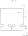
- FIG. 1 is a plan view illustrating a display device according to an embodiment of the present invention.
- a display device 1000 may include a display panel PNL, at least one connection film CF, and at least one printed circuit board PCB.
- the display panel PNL may be connected to the connection film CF. At least one pixel PX may be disposed on the display panel PNL.
- the pixel PX may generate a driving current by using a signal and/or a voltage applied through the connection film CF.
- the pixel PX may emit light corresponding to the driving current. As light is emitted from the pixel PX, the display panel PNL may display an image.
- a data line DL extending in a first direction D1 may be disposed on the display panel PNL.
- the data line DL may be connected to the connection film CF and the pixel PX, and may provide a data voltage to the pixel PX.
- connection film CF may be connected to the display panel PNL and the printed circuit board PCB.
- the connection film CF may electrically connect the display panel PNL and the printed circuit board PCB.
- film pads e.g., a film pads FP of FIG. 2
- a film align pad e.g., a first film align pad FAP1 of FIG. 2
- the film pads and the film align pad may connect the connection film CF to the printed circuit board PCB.
- connection film CF may be disposed on one side of the display panel PNL, and may be arranged side by side in a second direction D2 intersecting the first direction D 1.
- the printed circuit board PCB may be connected to the connection film CF.
- the printed circuit board PCB may be electrically connected to the display panel PNL through the connection film CF.
- board pads e.g., board pads BP of FIG. 2
- a board align pad e.g., a first board align pad BAP1 of FIG. 2
- the board pads and the board align pad may connect the printed circuit board PCB to the connection film CF.
- the printed circuit board PCB may be disposed on one side of the connection film CF, and may be arranged side by side in the second direction D2.
- FIG. 2 is an enlarged exploded perspective view of area A of FIG. 1 .
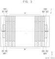
- FIG. 3 is an enlarged plan view of area A of FIG. 1 .
- FIG. 4 is a cross-sectional view taken along line I-I' of FIG. 3 .
- a first film align pad FAP1, film pads FP, and a second film align pad FAP2 may be disposed under the connection film CF.
- a first board align pad BAP1, board pads BP, and a second board align pad BAP2 may be disposed on the printed circuit board PCB.
- the second film align pad FAP2, the film pads FP, and the first film align pad FAP1 may be arranged side by side in the second direction D2.
- the film pads FP may be disposed between the first film align pad FAP1 and the second film align pad FAP2.
- the first film align pad FAP1 may include a first base lead BE1 and a first align lead AE1.
- the first base lead BE1 may extend in the first direction D1.
- the first align lead AE1 may protrude from the first base lead BE1 in the second direction D2.
- the film pads FP may be arranged side by side in the second direction D2. Each of the film pads FP may extend in the first direction D1.
- the shape of each of the film pads FP may be substantially the same as the shape of the first base lead BE1.
- the second film align pad FAP2 may include a second base lead BE2 and a second align lead AE2.
- the second base lead BE2 may extend in the first direction D1.
- the second align lead AE2 may protrude from the second base lead BE2 in a direction opposite to the second direction D2.
- the board align pad BAP2, the board pads BP, and the first board align pad BAP1 may be arranged side by side in the second direction D2.
- the board pads BP may be disposed between the first board align pad BAP1 and the second board align pad BAP2.
- the first board align pad BAP1 may include a first base land BA1 and a first align land AA1.
- the first base land BA1 may extend in the first direction D1.
- the first align land AA1 may protrude from the first base land BA1 in the second direction D2.
- the board pads BP may be arranged side by side in the second direction D2. Each of the board pads BP may extend in the first direction D1.
- the shape of each of the board pads BP may be substantially the same as the shape of the first base land BA1.
- the second board align pad BAP2 may include a second base land BA2 and a second align land AA2.
- the second base land BA2 may extend in the first direction D1.
- the second align land AA2 may protrude from the second base land BA2 in a direction opposite to the second direction D2.
- the first base lead BE1 may at least partially overlap the first base land BA1.
- the first align lead AE1 may at least partially overlap the first align land AA1.
- the film pads FP may at least partially overlap the board pads BP, respectively.
- the second base lead BE2 may at least partially overlap the second base land BA2.
- the second align lead AE2 may at least partially overlap the second align land AA2.
- the first align lead AE1 may completely overlap the first align land AA1.
- the first align land AA1 may partially overlap the first align lead AE1.
- a length of the first align lead AE1 in the first direction D1 may be smaller than a length of the first align land AA1 in the first direction D1.
- a length of the first align lead AE1 in the second direction D2 may be substantially the same as a length of the first align land AA1 in the second direction D2.
- the second align lead AE2 may completely overlap the second align land AA2.
- the second align land AA2 may partially overlap the second align lead AE2.
- a length of the second align lead AE2 in the first direction D1 may be smaller than a length of the second align land AA2 in the first direction D1.
- a length of the second align lead AE2 in the second direction D2 may be substantially the same as a length of the second align land AA2 in the second direction D2.
- the first base lead BE1 may contact the first base land BA1.
- the first align lead AE1 may contact the first align land AA1.
- the film pads FP may contact the board pads BP, respectively.
- the second base lead BE2 may contact the second base land BA2.
- the second align lead AE2 may contact the second align land AA2.
- FIG. 5 is a cross-sectional view illustrating a display panel included in the display device of FIG. 1 .
- the display panel PNL may include a substrate SUB, a lower conductive pattern MI,1, a first insulating layer IL1, an active pattern ACT, a second insulating layer IL2, a gate electrode GAT, a third insulating layer IL3, a first upper conductive pattern ML2, a second upper conductive pattern ML3, a fourth insulating layer IL4, a first electrode ADE, a pixel defining layer PDL, an emission layer EL, a second electrode CTE, and an encapsulation layer ENC.
- the substrate SUB may include a transparent or opaque material.
- Examples of the material that can be used as the substrate SUB may include glass, quartz, plastic, or the like. These may be used alone or in combination with each other.
- the lower conductive pattern ML1 may be disposed on the substrate SUB.
- the lower conductive pattern ML1 may be formed of a metal, an alloy, a conductive metal oxide, a transparent conductive material, or the like.
- materials that can be used as the lower conductive pattern ML1 may include silver ("Ag"), an alloy containing silver, molybdenum ("Mo”), an alloy containing molybdenum, aluminum (“Al”), an alloy containing aluminum, aluminum nitride (“AIN”), tungsten ("W”), tungsten nitride (“WN”), copper (“Cu”), nickel (“Ni”), chromium (“Cr”), chromium nitride (“CrN”), titanium ("Ti”), tantalum (“Ta”), platinum (“Pt”), scandium (“Sc”), indium tin oxide (“ITO”), indium zinc oxide (“IZO”), and the like. These may be used alone or in combination with each other.
- the first insulating layer IL1 may be disposed on the lower conductive pattern MI,1.
- the first insulating layer IL1 may be formed of an insulating material.
- the insulating material that can be used as the first insulating layer IL1 may include silicon oxide, silicon nitride, silicon oxynitride, and the like. These may be used alone or in combination with each other.
- the first insulating layer IL1 may be formed of a single layer or may be formed of multiple layers.
- the active pattern ACT may be disposed on the first insulating layer IL1.
- the active pattern ACT may be formed of a silicon semiconductor material or an oxide semiconductor material.
- the silicon semiconductor material that may be used as the active pattern ACT may include amorphous silicon, polycrystalline silicon, or the like.
- the oxide semiconductor material that may be used as the active pattern ACT may include IGZO (InGaZnO) and ITZO (InSnZnO).
- the oxide semiconductor material may further include indium (“In”), gallium (“Ga”), tin (“Sn”), zirconium (“Zr”), vanadium (“V”), hafnium (“Hf'), cadmium (“Cd”), germanium (“Ge”), chromium (“Cr”), titanium (“Ti”), and zinc (“Zn”). These may be used alone or in combination with each other.
- the second insulating layer IL2 may be disposed on the active pattern ACT.
- the second insulating layer IL2 may be formed of an insulating material.
- the insulating material that can be used as the second insulating layer IL2 may include silicon oxide, silicon nitride, silicon oxynitride, and the like. These may be used alone or in combination with each other.
- the second insulating layer IL2 may be formed of a single layer or may be formed of multiple layers.
- the gate electrode GAT may be disposed on the second insulating layer IL2.
- the gate electrode GAT may be formed of a metal, an alloy, a conductive metal oxide, a transparent conductive material, or the like.
- the material that can be used as the gate electrode GAT may include silver ("Ag"), an alloy containing silver, molybdenum ("Mo”), an alloy containing molybdenum, aluminum (“Al”), an alloy containing aluminum, aluminum nitride (“AIN”), tungsten ("W”), tungsten nitride (“WN”), copper (“Cu”), nickel (“Ni”), chromium (“Cr”), chromium nitride (“CrN”), titanium ("Ti”), tantalum (“Ta”), platinum (“Pt”), scandium (“Sc”), indium tin oxide (“ITO”), indium zinc oxide (“IZO”), and the like. These may be used alone or in combination with each other.
- the gate electrode GAT may be formed of
- the third insulating layer IL3 may be disposed on the gate electrode GAT.
- the third insulating layer IL3 may be formed of an insulating material. Examples of the insulating material that can be used as the third insulating layer IL3 may include silicon oxide, silicon nitride, silicon oxynitride, and the like. These may be used alone or in combination with each other.
- the third insulating layer IL3 may be formed of a single layer or may be formed of multiple layers.
- the first upper conductive pattern ML2 and the second upper conductive pattern ML3 may be disposed on the third insulating layer IL3.
- the first upper conductive pattern ML2 and the second upper conductive pattern ML3 may be formed together and may include the same material.
- the first upper conductive pattern ML2 and the second upper conductive pattern ML3 may be formed of a metal, an alloy, a conductive metal oxide, a transparent conductive material, or the like.
- materials that may be used as the first upper conductive pattern ML2 and the second upper conductive pattern ML3 may include silver ("Ag"), an alloy containing silver, molybdenum ("Mo”), an alloy containing molybdenum, aluminum (“Al”), an alloy containing aluminum, aluminum nitride (“AIN”), tungsten ("W”), tungsten nitride (“WN”), copper (“Cu”), nickel (“Ni”), chromium (“Cr”), chromium nitride (“CrN”), titanium ("Ti”), tantalum (“Ta”), platinum (“Pt”), scandium (“Sc”), indium tin oxide (“ITO”), indium zinc oxide (“IZO”), and the like. These may be used alone or in combination with each other.
- Mo molyb
- the first upper conductive pattern ML2 may contact the first lower conductive pattern ML1 and the active pattern ACT.
- the second upper conductive pattern ML3 may contact the active pattern ACT.
- the fourth insulating layer IL4 may be disposed on the first and second upper conductive patterns ML2 and ML3.
- the fourth insulating layer IL4 may be formed of an organic insulating material and/or an inorganic insulating material.
- the organic insulating material that can be used as the fourth insulating layer IL4 include photoresist, polyacrylic resin, polyimide resin, acrylic resin, and the like.
- the inorganic insulating material that can be used as the fourth insulating layer IL4 may include silicon oxide, silicon nitride, silicon oxynitride, and the like. These may be used alone or in combination with each other.
- the fourth insulating layer IL4 may be formed of a single layer or may be formed of multiple layers.
- the first electrode ADE may be disposed on the fourth insulating layer IL4.
- the first electrode ADE may be formed of a metal, an alloy, a conductive metal oxide, a transparent conductive material, or the like.
- materials that can be used as the first electrode ADE may include silver ("Ag"), an alloy containing silver, molybdenum ("Mo”), an alloy containing molybdenum, aluminum (“Al”), an alloy containing aluminum, aluminum nitride (“AIN”), tungsten ("W”), tungsten nitride (“WN”), copper (“Cu”), nickel (“Ni”), chromium (“Cr”), chromium nitride (“CrN”), titanium ("Ti”), tantalum (“Ta”), platinum (“Pt”), scandium (“Sc”), indium tin oxide (“ITO”), indium zinc oxide (“IZO”), and the like. These may be used alone or in combination with each other.
- the first electrode ADE may be formed of
- the pixel defining layer PDL may be disposed on the fourth insulating layer IL4.
- An opening exposing the first electrode ADE may be formed in the pixel defining layer PDL.
- the emission layer EL may be disposed in the opening on the first electrode ADE.
- the emission layer EL may emit light in response to the driving current.
- the second electrode CTE may be disposed on the emission layer EL.
- the encapsulation layer ENC may be disposed on the second electrode CTE.
- the encapsulation layer ENC may include at least one inorganic layer and at least one organic layer, and may prevent penetration of air and/or moisture.
- FIG. 6 is a diagram illustrating a reel which provides a connection film.
- a reel RL may provide the connection film CF included in the display device 1000 of FIG. 1 .
- the connection film CF may be wound on the reel RL in the form of a roll.
- connection film CF may have different degrees of curvature depending on the length at which the connection film CF is stored from the center of the reel RL. For example, a first degree of curvature CV1 of the first connection film CF1 positioned at an outer diameter of the reel RL may be different from a second degree of curvature CV2 of the second connection film CF2 positioned at an inner diameter of the reel RL.
- connection film CF and the printed circuit board PCB may be realigned in the first direction D1, according to the degree of curvature of the connection film CF. Accordingly, the connection film CF may be precisely aligned with the printed circuit board PCB in the first direction D1.
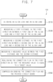
- FIG. 7 is a flowchart illustrating a method of manufacturing a display device according to an embodiment of the present invention.
- FIGS. 8 to 13 are diagrams illustrating a method of manufacturing a display device including a connection film having a first degree of curvature, according to the method of FIG. 7 .
- the display panel PNL on which the first connection film CF1 is disposed and the printed circuit board PCB may be aligned. Accordingly, the first align lead AE1 and the first align land AA1 may be aligned S110.
- a first distance Y1' in the first direction D1 between a first end of the first align lead AE1 and a first end of the first align land AA1 may be measured S120.
- the first end of the first align lead AE1 and the first end of the first align land AA1 may be adjacent to each other.
- a second distance Y2' in the first direction D1 between a second end of the first align lead AE1 and a second end of the first align land AA1 may be measured S130.
- the second end of the first align lead AE1 and the second end of the first align land AA1 may be adjacent to each other.
- a measured value between the first distance Y1' and the second distance Y2' may be measured S140.
- the measured value may be a difference between the first distance Y1' and the second distance Y2'.
- the measured value may be the difference (Y1'-Y2') between the first distance (Y1') and the second distance (Y2'), and may be about 2 ⁇ m.
- the film pads FP and the board pads BP may at least partially overlap each other while being misaligned in the first direction D1.
- the first connection film CF1 may be realigning in the first direction D1 so that the measured value is the same as a target value S150.
- the printed circuit board PCB may be fixed in the first direction D1, and the first connection film CF1 may move in the first direction D1.
- the target value may be a predetermined value according to the first degree of curvature CV1 of the first connection film CF1.
- the target value may be set according to the degree of curvature of the connection film.
- the first connection film CF1 and the printed circuit board PCB may be compression bonded S160 to each other. Accordingly, the film pads FP may contact the board pads BP, respectively.
- the first film align pad FAP1 may contact the first board align pad BAP1
- the second film align pad FAP2 may contact the second board align pad BAP2.
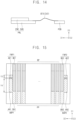
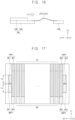
- FIGS. 14 to 19 are diagrams illustrating a method of manufacturing a display device including a connection film having a second degree of curvature, according to the method of FIG. 7 .
- the display panel PNL on which the second connection film CF2 is disposed and the printed circuit board PCB may be aligned. Accordingly, the first align lead AE1 and the first align land AA1 may be aligned S110.
- a first distance Y3' in the first direction D1 between a first end of the first align lead AE1 and a first end of the first align land AA1 may be measured S120.
- the first end of the first align lead AE1 and the first end of the first align land AA1 may be adjacent to each other.
- a second distance Y4' in the first direction D1 between a second end of the first align lead AE1 and a second end of the first align land AA1 may be measured S130.
- the second end of the first align lead AE1 and the second end of the first align land AA1 may be adjacent to each other.
- a measured value between the first distance Y3' and the second distance Y4' may be measured S140.
- the measured value may be a difference between the first distance Y3' and the second distance Y4'.
- the measured value may be the difference (Y3'-Y4') between the first distance (Y3') and the second distance (Y4'), and may be about -2 ⁇ m.
- the film pads FP and the board pads BP may at least partially overlap each other while being misaligned in the first direction D1.
- the second connection film CF2 may be realigned in the first direction D1 so that the measured value is the same as the target value S150.
- the printed circuit board PCB may be fixed in the first direction D1, and the second connection film CF2 may move in a direction opposite to the first direction D1.
- the target value may be a predetermined value according to the second degree of curvature CV2 of the second connection film CF2.
- the target value may be set according to the degree of curvature of the connection film.
- the target value when the second connection film CF2 has the second degree of curvature CV2, the target value may be about -1 ⁇ m.
- the second connection film CF2 may be moved in a direction opposite to the first direction D1 so that the measured value (e.g., -2 ⁇ m) is equal to the target value (e.g., -1 ⁇ m). Accordingly, the second connection film CF2 may be precisely aligned with the printed circuit board PCB in the first direction D1.
- the second connection film CF2 and the printed circuit board PCB may be compression bonded S160 to each other. Accordingly, the film pads FP may contact the board pads BP, respectively.
- the first film align pad FAP1 may contact the first board align pad BAP1
- the second film align pad FAP2 may contact the second board align pad BAP2.
- a first distance between the first end of the align lead and the first end of the align land may be measured, and a second distance between the second end of the align lead and the second end of the align land may be measured, and a measured value between the first distance and the second distance may be measured.
- the connection film may be realigned in the first direction so that the measured value is the same as a target value set according to the degree of curvature of the connection film. Accordingly, even if the connection films have different degrees of curvature, the film pads and the board pads may contact each other with a constant contact area in the first direction.
- FIG. 20 is a plan view illustrating a display device according to an embodiment of the present invention.
- FIG. 21 is an enlarged plan view of area B of FIG. 20 .
- FIG. 22 is a plan view illustrating a printed circuit board shown in the FIG. 21 .
- FIG. 23 is a plan view illustrating a connection film shown in the FIG. 21 . It is to be understood that any of the elements shown in FIG. 20 may be substituted and recombined with any of the elements shown in FIG. 1 .
- a display device 2000 may include a display panel PNL, at least one connection film CF, and at least one printed circuit board PCB.
- a first film align pad FAP1, film pads FP, and a second film align pad FAP2 may be disposed under the connection film CF.
- a first board align pad BAP1', board pads BP, and a second board align pad BAP2' may be disposed on the printed circuit board PCB.
- the display device 2000 may be substantially the same as the display device 1000 described with reference to FIG. 1 , except for the first board align pad BAP1' and the second board align pad BAP2'.
- the first board align pad BAP1', the board pads BP, and the second board align pad BAP2' may be arranged side by side in the second direction D2.
- the board pads BP may be disposed between the first board align pad BAP1' and the second board align pad BAP2'.
- the first board align pad BAP1' may include a first base land BA1', a first align land AA11', and a second align land AA12'.
- the first base land BA1' may extend in the first direction D1.
- the first align land AA11' and the second align land AA12' may protrude from the first base land BA1' in the second direction D2.
- the first align land AA11' and the second align land AA12' may be spaced apart from each other in the first direction D1.
- the board pads BP may be arranged side by side in the second direction D2. Each of the board pads BP may extend in the first direction D1.
- the shape of each of the board pads BP may be substantially the same as the shape of the first base land BA1'.
- the second board align pad BAP2' may include a second base land BA2', a third align land AA21', and a fourth align land AA22'.
- the second base land BA2' may extend in the first direction D1.
- the third align land AA21' and the fourth align land AA22' may protrude from the second base land BA2' in a direction opposite to the second direction D2.
- the third align land AA21' and the fourth align land AA22' may be spaced apart from each other in the first direction D1.
- the second film align pad FAP2, the film pads FP, and the first film align pad FAP1 may be arranged side by side in the second direction D2.
- the film pads FP may be disposed between the first film align pad FAP1 and the second film align pad FAP2.
- the first film align pad FAP1 may include a first base lead BE1 and a first align lead AE1.
- the first base lead BE1 may extend in the first direction D1.
- the first align lead AE1 may protrude from the first base lead BE1 in the second direction D2.
- the film pads FP may be arranged side by side in the second direction D2. Each of the film pads FP may extend in the first direction D1.
- the shape of each of the film pads FP may be substantially the same as the shape of the first base lead BE1.
- the second film align pad FAP2 may include a second base lead BE2 and a second align lead AE2.
- the second base lead BE2 may extend in the first direction D1.
- the second align lead AE2 may protrude from the second base lead BE2 in a direction opposite to the second direction D2.
- the first align lead AE1 and the first align land AA11' might not overlap each other.
- the first align lead AE1 and the second align land AA12' might not overlap each other.
- a length of the first align lead AE1 in the second direction D2 may be substantially the same as a length of the first align land AA11' in the second direction D2 and may be substantially the same as a length of the second align land AA12' in the second direction D2.
- a measured value between a first distance Y1 between a first end of the first align lead AE1 and a first end of the first align land AA11' and a second distance Y2 between a second end of the first align lead AE1 and a second end of the second align land AA12' may be measured, and the measured value may be applied to the method S100 described with reference to FIG. 7 , so that the film pads FP and the board pads BP may be precisely aligned.
- FIG. 24 is a plan view illustrating a display device according to an embodiment of the present invention.
- FIG. 25 is an enlarged plan view of area C of FIG. 24 .
- FIG. 26 is a plan view illustrating a printed circuit board shown in the FIG. 25 .
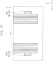
- FIG. 27 is a plan view illustrating a connection film shown in the FIG. 25 . It is to be understood that any of the elements shown in FIG. 20 may be substituted and recombined with any of the elements shown in FIG. 1 and/or FIG. 20 .
- a display device 3000 may include a display panel PNL, at least one connection film CF, and at least one printed circuit board PCB.
- a first film align pad FAP1", a film pad FP, and a second film align pad FAP2" may be disposed under the connection film CF.
- a first board align pad BAP1", board pads BP, and a second board align pad BAP2" may be disposed on the printed circuit board PCB.
- the first board align pad BAP1", the board pads BP, and the second board align pad BAP2" may be arranged in the second direction D2.
- the board pads BP may be disposed between the first board align pad BAP1" and the second board align pad BAP2".
- the first board align pad BAP1" may include a first base land BA1" and a first align land AA1".
- the first base land BA1" may extend in the first direction D1.
- the first align land AA1" may protrude from the first base land BA1" in the second direction D2.
- the board pads BP may be arranged side by side in the second direction D2.
- Each of the board pads BP may extend in the first direction D1.
- the shape of each of the board pads BP may be substantially the same as the shape of the first base land BA1".
- the second board align pad BAP2" may include a second base land BA2" and a second align land AA2".
- the second base land BA2" may extend in the first direction D1.
- the second align land AA2" may protrude from the second base land BA2" in a direction opposite to the second direction D2.
- the second film align pad FAP2", the film pads FP, and the first film align pad FAP1" may be arranged in the second direction D2.
- the film pads FP may be disposed between the first film align pad FAP1" and the second film align pad FAP2".
- the first film align pad FAP1" may include a first base lead BE1" and a first align lead AE1".
- the first base lead BE1" may extend in the first direction D1.
- the first align lead AE1" may protrude from the first base lead BE1" in the second direction D2.
- the film pads FP may be arranged side by side in the second direction D2. Each of the film pads FP may extend in the first direction D1.
- the shape of each of the film pads FP may be substantially the same as the shape of the first base lead BE1".
- the second film align pad FAP2" may include a second base lead BE2" and a second align lead AE2".
- the second base lead BE2" may extend in the first direction D1.
- the second align lead AE2" may protrude from the second base lead BE2" in a direction opposite to the second direction D2.
- the first align lead AE1" may partially overlap the first align land AA1".
- the first align land AA1" may partially overlap the first align lead AE1".
- a length of the first align lead AE1 " in the first direction D1 may be greater than a length of the first align land AA1" in the first direction D1.
- a length of the first align lead AE1" in the second direction D2 may be smaller than a length of the first align land AA1" in the second direction D2.
- the present invention can be applied to a display device.
- the present invention can be applied to display devices such as high-resolution smartphones, mobile phones, smart pads, smart watches, tablet PCs, vehicle navigation systems, televisions, computer monitors, and laptops.
- a display device PNL a display panel CF: a connection film PCB: a printed circuit board
- FAP1 a first film align pad FP: a film pads
- BAP1 a first board align pad BP: a board pads
- BE1 a first base lead AE1: a first align lead BA1: a first base land AA1: a first align land
Landscapes
- Engineering & Computer Science (AREA)
- Microelectronics & Electronic Packaging (AREA)
- Physics & Mathematics (AREA)
- Manufacturing & Machinery (AREA)
- Nonlinear Science (AREA)
- Metallurgy (AREA)
- Chemical & Material Sciences (AREA)
- Crystallography & Structural Chemistry (AREA)
- Mathematical Physics (AREA)
- General Physics & Mathematics (AREA)
- Optics & Photonics (AREA)
- Electroluminescent Light Sources (AREA)
- Devices For Indicating Variable Information By Combining Individual Elements (AREA)
Abstract
Description
- The present disclosure relates to a display device and, more specifically, to a display device and a method of manufacturing the display device.
- A display device generally includes a display panel, a connection film, and a printed circuit board. The printed circuit board generates a signal and/or voltage for driving the display panel, and the connection film is used to transmit the signal and/or the voltage from the printed circuit board to the display panel. In particular, the connection film includes a set of film pads and the printed circuit board includes a set of board pads. The display panel is directly connected to the connection film and the film pads make contract with the board pads to complete the connection between the display panel and the printed circuit board.
- To increase the quality of the display device (e.g., increase the display resolution, increase display frequency, etc.), research to reduce the spacing between the film pads and the board pads has been recently conducted.
- Aspects of some embodiments of the present disclosure related generally to a display device.
- Aspects of some embodiments of the present disclosure related generally to a method of manufacturing the display device.
- However, aspects of some embodiments of the present invention is not limited to the above-mentioned aspects, and may be expanded in various ways without departing from the spirit and scope of the present invention.
- A display device includes a film align pad disposed under a connection film that is connected to a display panel. The display device further including a base lead and an align lead. The base lead extends in a first direction and the align lead protrudes from the base lead in a second direction intersecting the first direction. A board align pad is disposed on a printed circuit board connected to the connection film and the board align pad includes a base land and an align land. The base land extends in the first direction and the align land protrudes from the base land in the second direction.
- The align lead may completely overlap the align land and the align land may partially overlaps the align lead.
- A length of the align lead in the first direction may be smaller than a length of the align land in the first direction.
- A length of the align lead in the second direction may be equal to a length of the align land in the second direction.
- The align lead and the align land might not overlap each other.
- A length of the align lead in the second direction may be equal to a length of the align land in the second direction.
- The align lead may partially overlap the align land and the align land may partially overlap the align lead.
- A length of the align lead in the first direction may be greater than a length of the align land in the first direction.
- A length of the align lead in the second direction may be smaller than a length of the align land in the second direction.
- The display device may further include film pads disposed under the connection film and arranged in the second direction. The film align pad may be arranged in the second direction together with the film pads.
- The display device may further include board pads disposed on the printed circuit board and arranged in the second direction. The board align pad may be arranged in the second direction together with the board pads.
- A method of manufacturing a display device includes aligning an align lead disposed under a connection film and an align land disposed on a printed circuit board. A first distance in a first direction between a first end of the align lead and a first end of the align land is measured. A second distance in the first direction between a second end of the align lead and a second end of the align land is measured. The connection film and the printed circuit board are realigned in the first direction so that a measured value between the first distance and the second distance is equal to a target value.
- The target value may be set according to a degree of curvature of the connection film.
- The connection film may be provided in a reel.
- A degree of curvature of the connection film positioned at an outer diameter of the reel may be different from a degree of curvature of the connection film positioned at an inner diameter of the reel.
- While the connection film and the printed circuit board are realigned in the first direction, the printed circuit board may be fixed in the first direction and the connection film may move in the first direction.
- The measured value may be a difference between the first distance and the second distance.
- The align lead may be disposed under the connection film and may protrude from a base lead in a second direction intersecting the first direction, and the base lead may extend in the first direction.
- The align land may be disposed on the printed circuit board and may protrude from a base land in the second direction, and the base land may extend in the first direction.
- The method may further include compression bonding the connection film and the printed circuit board, after the realigning the connection film and the printed circuit board in the first direction.
- Therefore, a display device according to example embodiments may include a film align pad disposed under the connection film and a board align pad disposed on the printed circuit board. The film align pad may include a base lead and an align lead protruding from the base lead, and the board align pad may include a base land and an align land protruding from the base land.
- In the method of manufacturing the display device, a first distance between a first end of an align lead and a first end of an align land may be measured, and a second distance between a second end of the align lead and a second end of the align land may be measured. The measured value between the first distance and the second distance may be measured. The connection film may be realigned so that the measured value is the same as a target value set according to the curvature of the connection film. Accordingly, even if the connection films have different curvatures, the film pads and the board pads may be compressed more precisely and may contact each other with a constant contact area.
- However, the effects of the present invention are not limited to the above-described effects, and may be expanded in various ways without departing from the spirit and scope of the present invention.
-
-
FIG. 1 is a plan view illustrating a display device according to an embodiment of the present invention. -
FIG. 2 is an enlarged exploded perspective view of area A ofFIG. 1 . -
FIG. 3 is an enlarged plan view of area A ofFIG. 1 . -
FIG. 4 is a cross-sectional view taken along line I-I' ofFIG. 3 . -
FIG. 5 is a cross-sectional view illustrating a display panel included in the display device ofFIG. 1 . -
FIG. 6 is a diagram illustrating a reel which provides a connection film. -
FIG. 7 is a flowchart illustrating a method of manufacturing a display device according to an embodiment of the present invention. -
FIGS. 8 to 13 are diagrams illustrating a method of manufacturing a display device including a connection film having a first degree of curvature, according to the method ofFIG. 7 . -
FIGS. 14 to 19 are diagrams illustrating a method of manufacturing a display device including a connection film having a second degree of curvature, according to the method ofFIG. 7 . -
FIG. 20 is a plan view illustrating a display device according to an embodiment of the present invention. -
FIG. 21 is an enlarged plan view of area B ofFIG. 20 . -
FIG. 22 is a plan view illustrating a printed circuit board shown in theFIG. 21 . -
FIG. 23 is a plan view illustrating a connection film shown in theFIG. 21 . -
FIG. 24 is a plan view illustrating a display device according to an embodiment of the present invention. -
FIG. 25 is an enlarged plan view of area C ofFIG. 24 . -
FIG. 26 is a plan view illustrating a printed circuit board shown in theFIG. 25 . -
FIG. 27 is a plan view illustrating a connection film shown in theFIG. 25 . - Embodiments of the present disclosure will be more clearly understood from the following detailed description in conjunction with the accompanying drawings.
-
FIG. 1 is a plan view illustrating a display device according to an embodiment of the present invention. - Referring to
FIG. 1 , adisplay device 1000, according to an embodiment of the present disclosure, may include a display panel PNL, at least one connection film CF, and at least one printed circuit board PCB. - The display panel PNL may be connected to the connection film CF. At least one pixel PX may be disposed on the display panel PNL. The pixel PX may generate a driving current by using a signal and/or a voltage applied through the connection film CF. In addition, the pixel PX may emit light corresponding to the driving current. As light is emitted from the pixel PX, the display panel PNL may display an image.
- In addition, a data line DL extending in a first direction D1 may be disposed on the display panel PNL. The data line DL may be connected to the connection film CF and the pixel PX, and may provide a data voltage to the pixel PX.
- The connection film CF may be connected to the display panel PNL and the printed circuit board PCB. The connection film CF may electrically connect the display panel PNL and the printed circuit board PCB. For example, film pads (e.g., a film pads FP of
FIG. 2 ) and a film align pad (e.g., a first film align pad FAP1 ofFIG. 2 ) may be disposed under the connection film CF. The film pads and the film align pad may connect the connection film CF to the printed circuit board PCB. - In an embodiment, the connection film CF may be disposed on one side of the display panel PNL, and may be arranged side by side in a second direction D2 intersecting the first direction D 1.
- The printed circuit board PCB may be connected to the connection film CF. The printed circuit board PCB may be electrically connected to the display panel PNL through the connection film CF. For example, board pads (e.g., board pads BP of
FIG. 2 ) and a board align pad (e.g., a first board align pad BAP1 ofFIG. 2 ) may be disposed on the printed circuit board PCB. The board pads and the board align pad may connect the printed circuit board PCB to the connection film CF. - In an embodiment, the printed circuit board PCB may be disposed on one side of the connection film CF, and may be arranged side by side in the second direction D2.
-
FIG. 2 is an enlarged exploded perspective view of area A ofFIG. 1 .FIG. 3 is an enlarged plan view of area A ofFIG. 1 .FIG. 4 is a cross-sectional view taken along line I-I' ofFIG. 3 . - Referring to
FIG. 2 , a first film align pad FAP1, film pads FP, and a second film align pad FAP2 may be disposed under the connection film CF. A first board align pad BAP1, board pads BP, and a second board align pad BAP2 may be disposed on the printed circuit board PCB. - The second film align pad FAP2, the film pads FP, and the first film align pad FAP1 may be arranged side by side in the second direction D2. The film pads FP may be disposed between the first film align pad FAP1 and the second film align pad FAP2.
- The first film align pad FAP1 may include a first base lead BE1 and a first align lead AE1. The first base lead BE1 may extend in the first direction D1. The first align lead AE1 may protrude from the first base lead BE1 in the second direction D2.
- The film pads FP may be arranged side by side in the second direction D2. Each of the film pads FP may extend in the first direction D1. For example, the shape of each of the film pads FP may be substantially the same as the shape of the first base lead BE1.
- The second film align pad FAP2 may include a second base lead BE2 and a second align lead AE2. The second base lead BE2 may extend in the first direction D1. The second align lead AE2 may protrude from the second base lead BE2 in a direction opposite to the second direction D2.
- The board align pad BAP2, the board pads BP, and the first board align pad BAP1 may be arranged side by side in the second direction D2. The board pads BP may be disposed between the first board align pad BAP1 and the second board align pad BAP2.
- The first board align pad BAP1 may include a first base land BA1 and a first align land AA1. The first base land BA1 may extend in the first direction D1. The first align land AA1 may protrude from the first base land BA1 in the second direction D2.
- The board pads BP may be arranged side by side in the second direction D2. Each of the board pads BP may extend in the first direction D1. For example, the shape of each of the board pads BP may be substantially the same as the shape of the first base land BA1.
- The second board align pad BAP2 may include a second base land BA2 and a second align land AA2. The second base land BA2 may extend in the first direction D1. The second align land AA2 may protrude from the second base land BA2 in a direction opposite to the second direction D2.
- Referring to
FIG. 3 , the first base lead BE1 may at least partially overlap the first base land BA1. The first align lead AE1 may at least partially overlap the first align land AA1. The film pads FP may at least partially overlap the board pads BP, respectively. The second base lead BE2 may at least partially overlap the second base land BA2. The second align lead AE2 may at least partially overlap the second align land AA2. - In an embodiment, the first align lead AE1 may completely overlap the first align land AA1. In addition, the first align land AA1 may partially overlap the first align lead AE1.
- For example, a length of the first align lead AE1 in the first direction D1 may be smaller than a length of the first align land AA1 in the first direction D1. In addition, a length of the first align lead AE1 in the second direction D2 may be substantially the same as a length of the first align land AA1 in the second direction D2.
- In an embodiment, the second align lead AE2 may completely overlap the second align land AA2. In addition, the second align land AA2 may partially overlap the second align lead AE2.
- For example, a length of the second align lead AE2 in the first direction D1 may be smaller than a length of the second align land AA2 in the first direction D1. In addition, a length of the second align lead AE2 in the second direction D2 may be substantially the same as a length of the second align land AA2 in the second direction D2.
- Referring to
FIG. 4 , the first base lead BE1 may contact the first base land BA1. The first align lead AE1 may contact the first align land AA1. The film pads FP may contact the board pads BP, respectively. The second base lead BE2 may contact the second base land BA2. The second align lead AE2 may contact the second align land AA2. -
FIG. 5 is a cross-sectional view illustrating a display panel included in the display device ofFIG. 1 . - Referring to
FIG. 5 , the display panel PNL may include a substrate SUB, a lower conductive pattern MI,1, a first insulating layer IL1, an active pattern ACT, a second insulating layer IL2, a gate electrode GAT, a third insulating layer IL3, a first upper conductive pattern ML2, a second upper conductive pattern ML3, a fourth insulating layer IL4, a first electrode ADE, a pixel defining layer PDL, an emission layer EL, a second electrode CTE, and an encapsulation layer ENC. - The substrate SUB may include a transparent or opaque material. Examples of the material that can be used as the substrate SUB may include glass, quartz, plastic, or the like. These may be used alone or in combination with each other.
- The lower conductive pattern ML1 may be disposed on the substrate SUB. In an embodiment, the lower conductive pattern ML1 may be formed of a metal, an alloy, a conductive metal oxide, a transparent conductive material, or the like. Examples of materials that can be used as the lower conductive pattern ML1 may include silver ("Ag"), an alloy containing silver, molybdenum ("Mo"), an alloy containing molybdenum, aluminum ("Al"), an alloy containing aluminum, aluminum nitride ("AIN"), tungsten ("W"), tungsten nitride ("WN"), copper ("Cu"), nickel ("Ni"), chromium ("Cr"), chromium nitride ("CrN"), titanium ("Ti"), tantalum ("Ta"), platinum ("Pt"), scandium ("Sc"), indium tin oxide ("ITO"), indium zinc oxide ("IZO"), and the like. These may be used alone or in combination with each other. In addition, the lower conductive pattern ML1 may be formed of a single layer or may be formed of multiple layers.
- The first insulating layer IL1 may be disposed on the lower conductive pattern MI,1. In an embodiment, the first insulating layer IL1 may be formed of an insulating material. Examples of the insulating material that can be used as the first insulating layer IL1 may include silicon oxide, silicon nitride, silicon oxynitride, and the like. These may be used alone or in combination with each other. In addition, the first insulating layer IL1 may be formed of a single layer or may be formed of multiple layers.
- The active pattern ACT may be disposed on the first insulating layer IL1. In an embodiment, the active pattern ACT may be formed of a silicon semiconductor material or an oxide semiconductor material. Examples of the silicon semiconductor material that may be used as the active pattern ACT may include amorphous silicon, polycrystalline silicon, or the like. Examples of the oxide semiconductor material that may be used as the active pattern ACT may include IGZO (InGaZnO) and ITZO (InSnZnO). In addition, the oxide semiconductor material may further include indium ("In"), gallium ("Ga"), tin ("Sn"), zirconium ("Zr"), vanadium ("V"), hafnium ("Hf'), cadmium ("Cd"), germanium ("Ge"), chromium ("Cr"), titanium ("Ti"), and zinc ("Zn"). These may be used alone or in combination with each other.
- The second insulating layer IL2 may be disposed on the active pattern ACT. In an embodiment, the second insulating layer IL2 may be formed of an insulating material. Examples of the insulating material that can be used as the second insulating layer IL2 may include silicon oxide, silicon nitride, silicon oxynitride, and the like. These may be used alone or in combination with each other. In addition, the second insulating layer IL2 may be formed of a single layer or may be formed of multiple layers.
- The gate electrode GAT may be disposed on the second insulating layer IL2. In an embodiment, the gate electrode GAT may be formed of a metal, an alloy, a conductive metal oxide, a transparent conductive material, or the like. Examples of the material that can be used as the gate electrode GAT may include silver ("Ag"), an alloy containing silver, molybdenum ("Mo"), an alloy containing molybdenum, aluminum ("Al"), an alloy containing aluminum, aluminum nitride ("AIN"), tungsten ("W"), tungsten nitride ("WN"), copper ("Cu"), nickel ("Ni"), chromium ("Cr"), chromium nitride ("CrN"), titanium ("Ti"), tantalum ("Ta"), platinum ("Pt"), scandium ("Sc"), indium tin oxide ("ITO"), indium zinc oxide ("IZO"), and the like. These may be used alone or in combination with each other. In addition, the gate electrode GAT may be formed of a single layer or may be formed of multiple layers.
- The third insulating layer IL3 may be disposed on the gate electrode GAT. In an embodiment, the third insulating layer IL3 may be formed of an insulating material. Examples of the insulating material that can be used as the third insulating layer IL3 may include silicon oxide, silicon nitride, silicon oxynitride, and the like. These may be used alone or in combination with each other. In addition, the third insulating layer IL3 may be formed of a single layer or may be formed of multiple layers.
- The first upper conductive pattern ML2 and the second upper conductive pattern ML3 may be disposed on the third insulating layer IL3. The first upper conductive pattern ML2 and the second upper conductive pattern ML3 may be formed together and may include the same material.
- In an embodiment, the first upper conductive pattern ML2 and the second upper conductive pattern ML3 may be formed of a metal, an alloy, a conductive metal oxide, a transparent conductive material, or the like. Examples of materials that may be used as the first upper conductive pattern ML2 and the second upper conductive pattern ML3 may include silver ("Ag"), an alloy containing silver, molybdenum ("Mo"), an alloy containing molybdenum, aluminum ("Al"), an alloy containing aluminum, aluminum nitride ("AIN"), tungsten ("W"), tungsten nitride ("WN"), copper ("Cu"), nickel ("Ni"), chromium ("Cr"), chromium nitride ("CrN"), titanium ("Ti"), tantalum ("Ta"), platinum ("Pt"), scandium ("Sc"), indium tin oxide ("ITO"), indium zinc oxide ("IZO"), and the like. These may be used alone or in combination with each other. In addition, the first upper conductive pattern ML2 and the second upper conductive pattern ML3 may be formed of a single layer or may be formed of multiple layers.
- The first upper conductive pattern ML2 may contact the first lower conductive pattern ML1 and the active pattern ACT. The second upper conductive pattern ML3 may contact the active pattern ACT.
- The fourth insulating layer IL4 may be disposed on the first and second upper conductive patterns ML2 and ML3. In an embodiment, the fourth insulating layer IL4 may be formed of an organic insulating material and/or an inorganic insulating material. Examples of the organic insulating material that can be used as the fourth insulating layer IL4 include photoresist, polyacrylic resin, polyimide resin, acrylic resin, and the like. Examples of the inorganic insulating material that can be used as the fourth insulating layer IL4 may include silicon oxide, silicon nitride, silicon oxynitride, and the like. These may be used alone or in combination with each other. In addition, the fourth insulating layer IL4 may be formed of a single layer or may be formed of multiple layers.
- The first electrode ADE may be disposed on the fourth insulating layer IL4. In an embodiment, the first electrode ADE may be formed of a metal, an alloy, a conductive metal oxide, a transparent conductive material, or the like. Examples of materials that can be used as the first electrode ADE may include silver ("Ag"), an alloy containing silver, molybdenum ("Mo"), an alloy containing molybdenum, aluminum ("Al"), an alloy containing aluminum, aluminum nitride ("AIN"), tungsten ("W"), tungsten nitride ("WN"), copper ("Cu"), nickel ("Ni"), chromium ("Cr"), chromium nitride ("CrN"), titanium ("Ti"), tantalum ("Ta"), platinum ("Pt"), scandium ("Sc"), indium tin oxide ("ITO"), indium zinc oxide ("IZO"), and the like. These may be used alone or in combination with each other. In addition, the first electrode ADE may be formed of a single layer or may be formed of multiple layers.
- The pixel defining layer PDL may be disposed on the fourth insulating layer IL4. An opening exposing the first electrode ADE may be formed in the pixel defining layer PDL.
- The emission layer EL may be disposed in the opening on the first electrode ADE. The emission layer EL may emit light in response to the driving current.
- The second electrode CTE may be disposed on the emission layer EL.
- The encapsulation layer ENC may be disposed on the second electrode CTE. The encapsulation layer ENC may include at least one inorganic layer and at least one organic layer, and may prevent penetration of air and/or moisture.
-
FIG. 6 is a diagram illustrating a reel which provides a connection film. - Referring to
FIG. 6 , a reel RL may provide the connection film CF included in thedisplay device 1000 ofFIG. 1 . The connection film CF may be wound on the reel RL in the form of a roll. - The connection film CF may have different degrees of curvature depending on the length at which the connection film CF is stored from the center of the reel RL. For example, a first degree of curvature CV1 of the first connection film CF1 positioned at an outer diameter of the reel RL may be different from a second degree of curvature CV2 of the second connection film CF2 positioned at an inner diameter of the reel RL.
- In the method of manufacturing a display device according to embodiments of the present invention, the connection film CF and the printed circuit board PCB may be realigned in the first direction D1, according to the degree of curvature of the connection film CF. Accordingly, the connection film CF may be precisely aligned with the printed circuit board PCB in the first direction D1.
-
FIG. 7 is a flowchart illustrating a method of manufacturing a display device according to an embodiment of the present invention.FIGS. 8 to 13 are diagrams illustrating a method of manufacturing a display device including a connection film having a first degree of curvature, according to the method ofFIG. 7 . - Referring to
FIGS. 7 and8 , in the method of manufacturing a display device S100 according to an embodiment of the present invention, the display panel PNL on which the first connection film CF1 is disposed and the printed circuit board PCB may be aligned. Accordingly, the first align lead AE1 and the first align land AA1 may be aligned S110. - Referring to
FIGS. 7 and9 , a first distance Y1' in the first direction D1 between a first end of the first align lead AE1 and a first end of the first align land AA1 may be measured S120. For example, the first end of the first align lead AE1 and the first end of the first align land AA1 may be adjacent to each other. - In addition, a second distance Y2' in the first direction D1 between a second end of the first align lead AE1 and a second end of the first align land AA1 may be measured S130. For example, the second end of the first align lead AE1 and the second end of the first align land AA1 may be adjacent to each other.
- A measured value between the first distance Y1' and the second distance Y2' may be measured S140. In an embodiment, the measured value may be a difference between the first distance Y1' and the second distance Y2'. For example, as shown in
FIG. 9 , the measured value may be the difference (Y1'-Y2') between the first distance (Y1') and the second distance (Y2'), and may be about 2 µm. In this case, the film pads FP and the board pads BP may at least partially overlap each other while being misaligned in the first direction D1. - Referring to
FIGS. 7 ,10 ,11 , and12 , the first connection film CF1 may be realigning in the first direction D1 so that the measured value is the same as a target value S150. In this case, the printed circuit board PCB may be fixed in the first direction D1, and the first connection film CF1 may move in the first direction D1. - In an embodiment, the target value may be a predetermined value according to the first degree of curvature CV1 of the first connection film CF1. For example, the target value may be set according to the degree of curvature of the connection film.
- For example, as shown in
FIGS. 10 and 11 , when the first connection film CF1 has the first degree of curvature CV1, the target value may be about 0 µm. The first connection film CF1 may be moved in the first direction D1 so that the measured value (e.g., 2 µm) is equal to the target value (e.g., 0 µm). Accordingly, the first connection film CF1 may be precisely aligned with the printed circuit board PCB in the first direction D1. - Referring to
FIGS. 7 and13 , the first connection film CF1 and the printed circuit board PCB may be compression bonded S160 to each other. Accordingly, the film pads FP may contact the board pads BP, respectively. In addition, the first film align pad FAP1 may contact the first board align pad BAP1, and the second film align pad FAP2 may contact the second board align pad BAP2. -
FIGS. 14 to 19 are diagrams illustrating a method of manufacturing a display device including a connection film having a second degree of curvature, according to the method ofFIG. 7 . - Referring to
FIGS. 7 and14 , in the method of manufacturing the display device S100 according to an embodiment of the present invention, the display panel PNL on which the second connection film CF2 is disposed and the printed circuit board PCB may be aligned. Accordingly, the first align lead AE1 and the first align land AA1 may be aligned S110. - Referring to
FIGS. 7 and15 , a first distance Y3' in the first direction D1 between a first end of the first align lead AE1 and a first end of the first align land AA1 may be measured S120. For example, the first end of the first align lead AE1 and the first end of the first align land AA1 may be adjacent to each other. - In addition, a second distance Y4' in the first direction D1 between a second end of the first align lead AE1 and a second end of the first align land AA1 may be measured S130. For example, the second end of the first align lead AE1 and the second end of the first align land AA1 may be adjacent to each other.
- A measured value between the first distance Y3' and the second distance Y4' may be measured S140. In an embodiment, the measured value may be a difference between the first distance Y3' and the second distance Y4'. For example, as shown in
FIG. 15 , the measured value may be the difference (Y3'-Y4') between the first distance (Y3') and the second distance (Y4'), and may be about -2 µm. In this case, the film pads FP and the board pads BP may at least partially overlap each other while being misaligned in the first direction D1. - Referring to
FIGS. 7 ,16 ,17 , and18 , the second connection film CF2 may be realigned in the first direction D1 so that the measured value is the same as the target value S150. In this case, the printed circuit board PCB may be fixed in the first direction D1, and the second connection film CF2 may move in a direction opposite to the first direction D1. - In an embodiment, the target value may be a predetermined value according to the second degree of curvature CV2 of the second connection film CF2. For example, the target value may be set according to the degree of curvature of the connection film.
- For example, as shown in
FIGS. 16 and 17 , when the second connection film CF2 has the second degree of curvature CV2, the target value may be about -1 µm. The second connection film CF2 may be moved in a direction opposite to the first direction D1 so that the measured value (e.g., -2 µm) is equal to the target value (e.g., -1 µm). Accordingly, the second connection film CF2 may be precisely aligned with the printed circuit board PCB in the first direction D1. - Referring to
FIGS. 7 and19 , the second connection film CF2 and the printed circuit board PCB may be compression bonded S160 to each other. Accordingly, the film pads FP may contact the board pads BP, respectively. In addition, the first film align pad FAP1 may contact the first board align pad BAP1, and the second film align pad FAP2 may contact the second board align pad BAP2. - In the manufacturing method S100 according to an embodiment of the present invention, a first distance between the first end of the align lead and the first end of the align land may be measured, and a second distance between the second end of the align lead and the second end of the align land may be measured, and a measured value between the first distance and the second distance may be measured. The connection film may be realigned in the first direction so that the measured value is the same as a target value set according to the degree of curvature of the connection film. Accordingly, even if the connection films have different degrees of curvature, the film pads and the board pads may contact each other with a constant contact area in the first direction.
-
FIG. 20 is a plan view illustrating a display device according to an embodiment of the present invention.FIG. 21 is an enlarged plan view of area B ofFIG. 20 .FIG. 22 is a plan view illustrating a printed circuit board shown in theFIG. 21 .FIG. 23 is a plan view illustrating a connection film shown in theFIG. 21 . It is to be understood that any of the elements shown inFIG. 20 may be substituted and recombined with any of the elements shown inFIG. 1 . - Referring to
FIG. 20 , adisplay device 2000, according to an embodiment, may include a display panel PNL, at least one connection film CF, and at least one printed circuit board PCB. - Referring to
FIG. 21 , a first film align pad FAP1, film pads FP, and a second film align pad FAP2 may be disposed under the connection film CF. A first board align pad BAP1', board pads BP, and a second board align pad BAP2' may be disposed on the printed circuit board PCB. - However, the
display device 2000 may be substantially the same as thedisplay device 1000 described with reference toFIG. 1 , except for the first board align pad BAP1' and the second board align pad BAP2'. - Referring to
FIG. 22 , the first board align pad BAP1', the board pads BP, and the second board align pad BAP2' may be arranged side by side in the second direction D2. The board pads BP may be disposed between the first board align pad BAP1' and the second board align pad BAP2'. - The first board align pad BAP1' may include a first base land BA1', a first align land AA11', and a second align land AA12'. The first base land BA1' may extend in the first direction D1. The first align land AA11' and the second align land AA12' may protrude from the first base land BA1' in the second direction D2. The first align land AA11' and the second align land AA12' may be spaced apart from each other in the first direction D1.
- The board pads BP may be arranged side by side in the second direction D2. Each of the board pads BP may extend in the first direction D1. For example, the shape of each of the board pads BP may be substantially the same as the shape of the first base land BA1'.
- The second board align pad BAP2' may include a second base land BA2', a third align land AA21', and a fourth align land AA22'. The second base land BA2' may extend in the first direction D1. The third align land AA21' and the fourth align land AA22' may protrude from the second base land BA2' in a direction opposite to the second direction D2. The third align land AA21' and the fourth align land AA22' may be spaced apart from each other in the first direction D1.
- Referring to
FIG. 23 , the second film align pad FAP2, the film pads FP, and the first film align pad FAP1 may be arranged side by side in the second direction D2. The film pads FP may be disposed between the first film align pad FAP1 and the second film align pad FAP2. - The first film align pad FAP1 may include a first base lead BE1 and a first align lead AE1. The first base lead BE1 may extend in the first direction D1. The first align lead AE1 may protrude from the first base lead BE1 in the second direction D2.
- The film pads FP may be arranged side by side in the second direction D2. Each of the film pads FP may extend in the first direction D1. For example, the shape of each of the film pads FP may be substantially the same as the shape of the first base lead BE1.
- The second film align pad FAP2 may include a second base lead BE2 and a second align lead AE2. The second base lead BE2 may extend in the first direction D1. The second align lead AE2 may protrude from the second base lead BE2 in a direction opposite to the second direction D2.
- Referring back to
FIG. 21 , in an embodiment, the first align lead AE1 and the first align land AA11' might not overlap each other. In addition, the first align lead AE1 and the second align land AA12' might not overlap each other. - A length of the first align lead AE1 in the second direction D2 may be substantially the same as a length of the first align land AA11' in the second direction D2 and may be substantially the same as a length of the second align land AA12' in the second direction D2.
- A measured value between a first distance Y1 between a first end of the first align lead AE1 and a first end of the first align land AA11' and a second distance Y2 between a second end of the first align lead AE1 and a second end of the second align land AA12' may be measured, and the measured value may be applied to the method S100 described with reference to
FIG. 7 , so that the film pads FP and the board pads BP may be precisely aligned. -
FIG. 24 is a plan view illustrating a display device according to an embodiment of the present invention.FIG. 25 is an enlarged plan view of area C ofFIG. 24 .FIG. 26 is a plan view illustrating a printed circuit board shown in theFIG. 25 .FIG. 27 is a plan view illustrating a connection film shown in theFIG. 25 . It is to be understood that any of the elements shown inFIG. 20 may be substituted and recombined with any of the elements shown inFIG. 1 and/orFIG. 20 . - Referring to
FIG. 24 , adisplay device 3000, according to an embodiment, may include a display panel PNL, at least one connection film CF, and at least one printed circuit board PCB. - Referring to
FIG. 25 , a first film align pad FAP1", a film pad FP, and a second film align pad FAP2" may be disposed under the connection film CF. A first board align pad BAP1", board pads BP, and a second board align pad BAP2" may be disposed on the printed circuit board PCB. - Referring to
FIG. 26 , the first board align pad BAP1", the board pads BP, and the second board align pad BAP2" may be arranged in the second direction D2. The board pads BP may be disposed between the first board align pad BAP1" and the second board align pad BAP2". - The first board align pad BAP1" may include a first base land BA1" and a first align land AA1". The first base land BA1" may extend in the first direction D1. The first align land AA1" may protrude from the first base land BA1" in the second direction D2.
- The board pads BP may be arranged side by side in the second direction D2. Each of the board pads BP may extend in the first direction D1. For example, the shape of each of the board pads BP may be substantially the same as the shape of the first base land BA1".
- The second board align pad BAP2" may include a second base land BA2" and a second align land AA2". The second base land BA2" may extend in the first direction D1. The second align land AA2" may protrude from the second base land BA2" in a direction opposite to the second direction D2.
- Referring to
FIG. 27 , the second film align pad FAP2", the film pads FP, and the first film align pad FAP1" may be arranged in the second direction D2. The film pads FP may be disposed between the first film align pad FAP1" and the second film align pad FAP2". - The first film align pad FAP1" may include a first base lead BE1" and a first align lead AE1". The first base lead BE1" may extend in the first direction D1. The first align lead AE1" may protrude from the first base lead BE1" in the second direction D2.
- The film pads FP may be arranged side by side in the second direction D2. Each of the film pads FP may extend in the first direction D1. For example, the shape of each of the film pads FP may be substantially the same as the shape of the first base lead BE1".
- The second film align pad FAP2" may include a second base lead BE2" and a second align lead AE2". The second base lead BE2" may extend in the first direction D1. The second align lead AE2" may protrude from the second base lead BE2" in a direction opposite to the second direction D2.
- Referring back to
FIG. 25 , in an embodiment, the first align lead AE1" may partially overlap the first align land AA1". In addition, the first align land AA1" may partially overlap the first align lead AE1". - A length of the first align lead AE1 " in the first direction D1 may be greater than a length of the first align land AA1" in the first direction D1. In addition, a length of the first align lead AE1" in the second direction D2 may be smaller than a length of the first align land AA1" in the second direction D2.
- A measured value between a first distance Y1 between a first end of the first align lead AE1" and a first end of the first align land AA1" and a second distance Y2 between a second end of the first align lead AE1" and a second end of the first align land AA1", and the measured value applied to the method S100 described with reference to
FIG. 7 , so that the film pads FP and the board pads BP may be precisely aligned. - Although certain embodiments and implementations have been described herein, other embodiments and modifications will be apparent from this description. Accordingly, the inventive concepts are not necessarily limited to the embodiments described herein, but rather various modifications and equivalent arrangements as would be apparent to a person of ordinary skill in the art are within the scope of the present disclosure.
- The present invention can be applied to a display device. For example, the present invention can be applied to display devices such as high-resolution smartphones, mobile phones, smart pads, smart watches, tablet PCs, vehicle navigation systems, televisions, computer monitors, and laptops.
- Although the present invention has been described above with reference to exemplary embodiments, those skilled in the art will understand that various modifications and changes can be made to the present invention without departing from the spirit and scope of the present invention as set forth in the claims below.
-
1000, 2000, 3000: a display device PNL: a display panel CF: a connection film PCB: a printed circuit board FAP1: a first film align pad FP: a film pads BAP1: a first board align pad BP: a board pads BE1: a first base lead AE1: a first align lead BA1: a first base land AA1: a first align land
Claims (20)
- A display device, comprising:a film align pad disposed under a connection film that is connected to a display panel, the film align pad including a base lead and an align lead, wherein the base lead extends in a first direction and the align lead protrudes from the base lead in a second direction intersecting the first direction; anda board align pad disposed on a printed circuit board that is connected to the connection film, the board align pad including a base land and an align land, wherein the base land extends in the first direction and the align land protrudes from the base land in the second direction.
- The display device of claim 1, wherein the align lead completely overlaps the align land, and
wherein the align land partially overlaps the align lead. - The display device of claim 2, wherein a length of the align lead in the first direction is smaller than a length of the align land in the first direction.
- The display device of claim 2, wherein a length of the align lead in the second direction is equal to a length of the align land in the second direction.
- The display device of claim 1, wherein the align lead and the align land do not overlap each other.
- The display device of claim 5, wherein a length of the align lead in the second direction is equal to a length of the align land in the second direction.
- The display device of claim 1, wherein the align lead partially overlaps the align land, and
wherein the align land partially overlaps the align lead. - The display device of claim 7, wherein a length of the align lead in the first direction is greater than a length of the align land in the first direction.
- The display device of claim 7, wherein a length of the align lead in the second direction is smaller than a length of the align land in the second direction.
- The display device of claim 1, further comprising:film pads disposed under the connection film and arranged in the second direction,wherein the film align pad is arranged in the second direction together with the film pads.
- The display device of claim 1, further comprising:board pads disposed on the printed circuit board and arranged in the second direction,wherein the board align pad is arranged in the second direction together with the board pads.
- A method of manufacturing a display device, the method comprising:aligning an align lead disposed under a connection film and an align land disposed on a printed circuit board;measuring a first distance in a first direction between a first end of the align lead and a first end of the align land;measuring a second distance in the first direction between a second end of the align lead and a second end of the align land; andrealigning the connection film and the printed circuit board in the first direction so that a measured value between the first distance and the second distance is equal to a target value.
- The method of claim 12, wherein the target value is set according to a degree of curvature of the connection film.
- The method of claim 12, wherein the connection film is provided in a reel.
- The method of claim 14, wherein a degree of curvature of the connection film positioned at an outer diameter of the reel is different from a degree of curvature of the connection film positioned at an inner diameter of the reel.
- The method of claim 12, wherein while the connection film and the printed circuit board are realigned in the first direction,wherein the printed circuit board is fixed in the first direction, andwherein the connection film moves in the first direction.
- The method of claim 12, wherein the measured value is a difference between the first distance and the second distance.
- The method of claim 12, wherein the align lead is disposed under the connection film and protrudes from a base lead in a second direction intersecting the first direction, and
wherein the base lead extends in the first direction. - The method of claim 18, wherein the align land is disposed on the printed circuit board and protrudes from a base land in the second direction, and
wherein the base land extends in the first direction. - The method of claim 12, further comprising:
compression bonding the connection film and the printed circuit board to each other after the realigning of the connection film and the printed circuit board in the first direction.
Applications Claiming Priority (2)
| Application Number | Priority Date | Filing Date | Title |
|---|---|---|---|
| KR1020220032758A KR102959372B1 (en) | 2022-03-16 | Display device and method of manufacturing the same | |
| PCT/KR2023/000652 WO2023177065A1 (en) | 2022-03-16 | 2023-01-13 | Display device and method of manufacturing same |
Publications (2)
| Publication Number | Publication Date |
|---|---|
| EP4496001A1 true EP4496001A1 (en) | 2025-01-22 |
| EP4496001A4 EP4496001A4 (en) | 2026-03-25 |
Family
ID=87532671
Family Applications (1)
| Application Number | Title | Priority Date | Filing Date |
|---|---|---|---|
| EP23770945.6A Pending EP4496001A4 (en) | 2022-03-16 | 2023-01-13 | Display device and method for manufacturing it |
Country Status (5)
| Country | Link |
|---|---|
| US (2) | US12402290B2 (en) |
| EP (1) | EP4496001A4 (en) |
| JP (1) | JP2025510003A (en) |
| CN (2) | CN116782710A (en) |
| WO (1) | WO2023177065A1 (en) |
Family Cites Families (14)
| Publication number | Priority date | Publication date | Assignee | Title |
|---|---|---|---|---|
| JP4742441B2 (en) * | 2001-04-16 | 2011-08-10 | 日本電気株式会社 | Connection structure between flexible printed circuit and wiring board, connection method thereof, liquid crystal display device and manufacturing method thereof |
| JP2007335421A (en) * | 2004-10-01 | 2007-12-27 | Sharp Corp | Circuit board connection structure and circuit board manufacturing method |
| KR20070117110A (en) | 2006-06-07 | 2007-12-12 | 엘지.필립스 엘시디 주식회사 | Tape carrier package and liquid crystal display including the same |
| KR100881183B1 (en) | 2006-11-21 | 2009-02-05 | 삼성전자주식회사 | Semiconductor chip having bumps of different heights and semiconductor package including the same |
| JP2013167694A (en) * | 2012-02-14 | 2013-08-29 | Japan Display Inc | Display device |
| JP6037682B2 (en) * | 2012-06-29 | 2016-12-07 | オリンパス株式会社 | Printed wiring board connection structure |
| KR102330449B1 (en) | 2015-10-01 | 2021-11-26 | 삼성디스플레이 주식회사 | Display apparatus |
| KR20170059523A (en) * | 2015-11-20 | 2017-05-31 | 삼성디스플레이 주식회사 | Display apparatus, tiled display apparatus and method of manufacturing the same |
| KR102481818B1 (en) | 2017-08-22 | 2022-12-28 | 삼성디스플레이 주식회사 | Electronic component, electric device including the same |
| KR102477230B1 (en) * | 2018-01-25 | 2022-12-13 | 삼성디스플레이 주식회사 | Display device |
| KR102603403B1 (en) | 2018-08-09 | 2023-11-17 | 삼성디스플레이 주식회사 | Display device |
| KR101979749B1 (en) | 2018-12-19 | 2019-05-17 | 주식회사 케이엔케이 | Device for inspecting flexible printed circuit board |
| CN209216555U (en) * | 2019-01-29 | 2019-08-06 | 合肥京东方显示技术有限公司 | A kind of flip chip and display device |
| KR102853326B1 (en) | 2020-07-08 | 2025-09-01 | 삼성디스플레이 주식회사 | Display apparatus |
-
2022
- 2022-10-27 US US18/050,421 patent/US12402290B2/en active Active
-
2023
- 2023-01-13 WO PCT/KR2023/000652 patent/WO2023177065A1/en not_active Ceased
- 2023-01-13 EP EP23770945.6A patent/EP4496001A4/en active Pending
- 2023-01-13 JP JP2024543475A patent/JP2025510003A/en active Pending
- 2023-03-06 CN CN202310201381.9A patent/CN116782710A/en active Pending
- 2023-03-06 CN CN202320387672.7U patent/CN219514544U/en active Active
-
2025
- 2025-07-22 US US19/276,211 patent/US20250351318A1/en active Pending
Also Published As
| Publication number | Publication date |
|---|---|
| KR20230135716A (en) | 2023-09-26 |
| JP2025510003A (en) | 2025-04-14 |
| US12402290B2 (en) | 2025-08-26 |
| CN116782710A (en) | 2023-09-19 |
| WO2023177065A1 (en) | 2023-09-21 |
| US20230301048A1 (en) | 2023-09-21 |
| EP4496001A4 (en) | 2026-03-25 |
| CN219514544U (en) | 2023-08-11 |
| US20250351318A1 (en) | 2025-11-13 |
Similar Documents
| Publication | Publication Date | Title |
|---|---|---|
| CN111462626B (en) | Foldable display device | |
| KR102677776B1 (en) | Organic light emitting display device | |
| EP3245678B1 (en) | Flexible display panel with bent substrate | |
| KR102953414B1 (en) | Manufacturing method of a cover window for a flexible display device and manufacturing method of the flexible display device | |
| US20170110529A1 (en) | Flexible Display Panel With Redundant Bent Signal Lines | |
| US11877469B2 (en) | Display device and manufacturing method thereof | |
| US10170728B2 (en) | Display device | |
| US11740751B2 (en) | Touch sensing unit and display device including same | |
| CN114256310A (en) | Display device | |
| US20240361870A1 (en) | Touch sensing unit and display device including the same | |
| CN115274777A (en) | Display device | |
| EP3940781B1 (en) | Display device and method for manufacturing the same | |
| KR102936615B1 (en) | Thin film transistor, method for fabricating the thin film transistor, thin film transistor array substrate, and method for fabricating the thin film transistor array substrate | |
| US20250040356A1 (en) | Display device and method of manufacturing the same | |
| EP4503896A1 (en) | Display device and method of fabricating the same | |
| KR102959372B1 (en) | Display device and method of manufacturing the same | |
| GB2638539A (en) | Display device | |
| CN219514544U (en) | Display device | |
| US20230006013A1 (en) | Display device | |
| KR20250112342A (en) | Display device and method of fabricating the same | |
| US12289968B2 (en) | Display device | |
| KR102912366B1 (en) | Display device | |
| EP4654798A1 (en) | Display device | |
| US20250151525A1 (en) | Display device including flow-control layer and method of providing the same | |
| EP4447642A1 (en) | Display device and method of manufacturing the same |
Legal Events
| Date | Code | Title | Description |
|---|---|---|---|
| STAA | Information on the status of an ep patent application or granted ep patent |
Free format text: STATUS: THE INTERNATIONAL PUBLICATION HAS BEEN MADE |
|
| PUAI | Public reference made under article 153(3) epc to a published international application that has entered the european phase |
Free format text: ORIGINAL CODE: 0009012 |
|
| STAA | Information on the status of an ep patent application or granted ep patent |
Free format text: STATUS: REQUEST FOR EXAMINATION WAS MADE |
|
| 17P | Request for examination filed |
Effective date: 20240913 |
|
| AK | Designated contracting states |
Kind code of ref document: A1 Designated state(s): AL AT BE BG CH CY CZ DE DK EE ES FI FR GB GR HR HU IE IS IT LI LT LU LV MC ME MK MT NL NO PL PT RO RS SE SI SK SM TR |
|
| DAV | Request for validation of the european patent (deleted) | ||
| DAX | Request for extension of the european patent (deleted) | ||
| REG | Reference to a national code |
Ref country code: DE Ref legal event code: R079 Free format text: PREVIOUS MAIN CLASS: H01L0027120000 Ipc: H05K0001020000 |
|
| A4 | Supplementary search report drawn up and despatched |
Effective date: 20260224 |
|
| RIC1 | Information provided on ipc code assigned before grant |
Ipc: H05K 1/02 20060101AFI20260218BHEP Ipc: H05K 3/36 20060101ALI20260218BHEP Ipc: H05K 1/14 20060101ALI20260218BHEP Ipc: G02F 1/1345 20060101ALI20260218BHEP Ipc: H05K 1/11 20060101ALN20260218BHEP Ipc: H05K 3/321 20260101ALN20260218BHEP Ipc: H05K 1/189 20260101ALN20260218BHEP |
|
| P01 | Opt-out of the competence of the unified patent court (upc) registered |
Free format text: CASE NUMBER: UPC_APP_0007482_4496001/2026 Effective date: 20260226 |