EP4495688A1 - Compound for forming metal-containing film, composition for forming metal-containing film, patterning process, and method for manufacturing compound for forming metal-containing film - Google Patents
Compound for forming metal-containing film, composition for forming metal-containing film, patterning process, and method for manufacturing compound for forming metal-containing film Download PDFInfo
- Publication number
- EP4495688A1 EP4495688A1 EP24183158.5A EP24183158A EP4495688A1 EP 4495688 A1 EP4495688 A1 EP 4495688A1 EP 24183158 A EP24183158 A EP 24183158A EP 4495688 A1 EP4495688 A1 EP 4495688A1
- Authority
- EP
- European Patent Office
- Prior art keywords
- metal
- group
- containing film
- forming
- compound
- Prior art date
- Legal status (The legal status is an assumption and is not a legal conclusion. Google has not performed a legal analysis and makes no representation as to the accuracy of the status listed.)
- Pending
Links
- 229910052751 metal Inorganic materials 0.000 title claims abstract description 397
- 239000002184 metal Substances 0.000 title claims abstract description 397
- 150000001875 compounds Chemical class 0.000 title claims abstract description 207
- 239000000203 mixture Substances 0.000 title claims abstract description 167
- 238000000034 method Methods 0.000 title claims abstract description 120
- 230000008569 process Effects 0.000 title claims abstract description 60
- 238000000059 patterning Methods 0.000 title claims abstract description 39
- 238000004519 manufacturing process Methods 0.000 title claims abstract description 34
- 125000004432 carbon atom Chemical group C* 0.000 claims abstract description 174
- 239000003446 ligand Substances 0.000 claims abstract description 154
- 125000000962 organic group Chemical group 0.000 claims abstract description 112
- 125000004435 hydrogen atom Chemical group [H]* 0.000 claims abstract description 45
- 229910052726 zirconium Inorganic materials 0.000 claims abstract description 29
- 125000004429 atom Chemical group 0.000 claims abstract description 26
- 229910052719 titanium Inorganic materials 0.000 claims abstract description 25
- 229910052735 hafnium Inorganic materials 0.000 claims abstract description 24
- 239000000758 substrate Substances 0.000 claims description 90
- 238000001312 dry etching Methods 0.000 claims description 59
- 150000002736 metal compounds Chemical class 0.000 claims description 54
- 229920002120 photoresistant polymer Polymers 0.000 claims description 42
- 239000002253 acid Substances 0.000 claims description 40
- 239000003960 organic solvent Substances 0.000 claims description 39
- 239000003431 cross linking reagent Substances 0.000 claims description 34
- 238000006243 chemical reaction Methods 0.000 claims description 26
- 239000000463 material Substances 0.000 claims description 25
- 238000004132 cross linking Methods 0.000 claims description 23
- 238000011161 development Methods 0.000 claims description 22
- 238000012545 processing Methods 0.000 claims description 21
- 238000009835 boiling Methods 0.000 claims description 18
- 125000003545 alkoxy group Chemical group 0.000 claims description 17
- 230000007062 hydrolysis Effects 0.000 claims description 17
- 238000006460 hydrolysis reaction Methods 0.000 claims description 17
- 238000010438 heat treatment Methods 0.000 claims description 16
- 125000003118 aryl group Chemical group 0.000 claims description 13
- 239000004094 surface-active agent Substances 0.000 claims description 13
- 125000004423 acyloxy group Chemical group 0.000 claims description 11
- 150000007942 carboxylates Chemical group 0.000 claims description 11
- 125000005843 halogen group Chemical group 0.000 claims description 11
- 108010009736 Protein Hydrolysates Proteins 0.000 claims description 10
- 239000007795 chemical reaction product Substances 0.000 claims description 10
- 125000000217 alkyl group Chemical group 0.000 claims description 9
- 125000001183 hydrocarbyl group Chemical group 0.000 claims description 7
- 150000003377 silicon compounds Chemical class 0.000 claims description 5
- 239000004065 semiconductor Substances 0.000 abstract description 5
- 239000010408 film Substances 0.000 description 586
- 239000010410 layer Substances 0.000 description 154
- -1 polyhydroxystyrene Polymers 0.000 description 51
- 230000000052 comparative effect Effects 0.000 description 46
- 238000005530 etching Methods 0.000 description 44
- 239000007789 gas Substances 0.000 description 40
- 239000002904 solvent Substances 0.000 description 31
- 150000002430 hydrocarbons Chemical group 0.000 description 28
- ARXJGSRGQADJSQ-UHFFFAOYSA-N 1-methoxypropan-2-ol Chemical compound COCC(C)O ARXJGSRGQADJSQ-UHFFFAOYSA-N 0.000 description 27
- 230000015572 biosynthetic process Effects 0.000 description 24
- 229910052710 silicon Inorganic materials 0.000 description 22
- 238000003786 synthesis reaction Methods 0.000 description 22
- XUIMIQQOPSSXEZ-UHFFFAOYSA-N Silicon Chemical compound [Si] XUIMIQQOPSSXEZ-UHFFFAOYSA-N 0.000 description 20
- 230000018109 developmental process Effects 0.000 description 20
- 239000010703 silicon Substances 0.000 description 20
- 239000000243 solution Substances 0.000 description 20
- 239000010936 titanium Substances 0.000 description 20
- VYPSYNLAJGMNEJ-UHFFFAOYSA-N Silicium dioxide Chemical compound O=[Si]=O VYPSYNLAJGMNEJ-UHFFFAOYSA-N 0.000 description 18
- 239000007858 starting material Substances 0.000 description 18
- LLHKCFNBLRBOGN-UHFFFAOYSA-N propylene glycol methyl ether acetate Chemical compound COCC(C)OC(C)=O LLHKCFNBLRBOGN-UHFFFAOYSA-N 0.000 description 16
- 229920000642 polymer Polymers 0.000 description 15
- RMCAUKPOUZTMOV-UHFFFAOYSA-N cyclohepta[d][1,3]thiazol-2-one Chemical compound C1=CC=CC=C2SC(=O)N=C21 RMCAUKPOUZTMOV-UHFFFAOYSA-N 0.000 description 14
- 125000003178 carboxy group Chemical group [H]OC(*)=O 0.000 description 11
- 229910052731 fluorine Inorganic materials 0.000 description 10
- 238000004528 spin coating Methods 0.000 description 10
- XLYOFNOQVPJJNP-UHFFFAOYSA-N water Substances O XLYOFNOQVPJJNP-UHFFFAOYSA-N 0.000 description 10
- MYMOFIZGZYHOMD-UHFFFAOYSA-N Dioxygen Chemical compound O=O MYMOFIZGZYHOMD-UHFFFAOYSA-N 0.000 description 9
- YCKRFDGAMUMZLT-UHFFFAOYSA-N Fluorine atom Chemical compound [F] YCKRFDGAMUMZLT-UHFFFAOYSA-N 0.000 description 9
- YXFVVABEGXRONW-UHFFFAOYSA-N Toluene Chemical compound CC1=CC=CC=C1 YXFVVABEGXRONW-UHFFFAOYSA-N 0.000 description 9
- 229910001882 dioxygen Inorganic materials 0.000 description 9
- 230000000694 effects Effects 0.000 description 9
- 239000011737 fluorine Substances 0.000 description 9
- 239000001301 oxygen Substances 0.000 description 9
- 229910052760 oxygen Inorganic materials 0.000 description 9
- 239000000377 silicon dioxide Substances 0.000 description 9
- QVGXLLKOCUKJST-UHFFFAOYSA-N atomic oxygen Chemical compound [O] QVGXLLKOCUKJST-UHFFFAOYSA-N 0.000 description 8
- 229910052681 coesite Inorganic materials 0.000 description 8
- 229910052906 cristobalite Inorganic materials 0.000 description 8
- 238000007654 immersion Methods 0.000 description 8
- 229920005989 resin Polymers 0.000 description 8
- 239000011347 resin Substances 0.000 description 8
- 239000002210 silicon-based material Substances 0.000 description 8
- 229910052682 stishovite Inorganic materials 0.000 description 8
- 229910052905 tridymite Inorganic materials 0.000 description 8
- 229910052799 carbon Inorganic materials 0.000 description 7
- 239000003054 catalyst Substances 0.000 description 7
- 125000001495 ethyl group Chemical group [H]C([H])([H])C([H])([H])* 0.000 description 7
- 238000011156 evaluation Methods 0.000 description 7
- 125000002887 hydroxy group Chemical group [H]O* 0.000 description 7
- VLKZOEOYAKHREP-UHFFFAOYSA-N n-Hexane Chemical compound CCCCCC VLKZOEOYAKHREP-UHFFFAOYSA-N 0.000 description 7
- 230000003287 optical effect Effects 0.000 description 7
- 239000002356 single layer Substances 0.000 description 7
- YEJRWHAVMIAJKC-UHFFFAOYSA-N 4-Butyrolactone Chemical compound O=C1CCCO1 YEJRWHAVMIAJKC-UHFFFAOYSA-N 0.000 description 6
- UHOVQNZJYSORNB-UHFFFAOYSA-N Benzene Chemical compound C1=CC=CC=C1 UHOVQNZJYSORNB-UHFFFAOYSA-N 0.000 description 6
- 101100257262 Caenorhabditis elegans soc-1 gene Proteins 0.000 description 6
- LRHPLDYGYMQRHN-UHFFFAOYSA-N N-Butanol Chemical compound CCCCO LRHPLDYGYMQRHN-UHFFFAOYSA-N 0.000 description 6
- QCWXUUIWCKQGHC-UHFFFAOYSA-N Zirconium Chemical compound [Zr] QCWXUUIWCKQGHC-UHFFFAOYSA-N 0.000 description 6
- 230000003667 anti-reflective effect Effects 0.000 description 6
- 229910052801 chlorine Inorganic materials 0.000 description 6
- 239000011248 coating agent Substances 0.000 description 6
- 238000000576 coating method Methods 0.000 description 6
- 125000002496 methyl group Chemical group [H]C([H])([H])* 0.000 description 6
- 229920000620 organic polymer Polymers 0.000 description 6
- 239000002994 raw material Substances 0.000 description 6
- JOLQKTGDSGKSKJ-UHFFFAOYSA-N 1-ethoxypropan-2-ol Chemical compound CCOCC(C)O JOLQKTGDSGKSKJ-UHFFFAOYSA-N 0.000 description 5
- ZAMOUSCENKQFHK-UHFFFAOYSA-N Chlorine atom Chemical compound [Cl] ZAMOUSCENKQFHK-UHFFFAOYSA-N 0.000 description 5
- 125000003710 aryl alkyl group Chemical group 0.000 description 5
- BSDOQSMQCZQLDV-UHFFFAOYSA-N butan-1-olate;zirconium(4+) Chemical compound [Zr+4].CCCC[O-].CCCC[O-].CCCC[O-].CCCC[O-] BSDOQSMQCZQLDV-UHFFFAOYSA-N 0.000 description 5
- 239000000460 chlorine Substances 0.000 description 5
- 239000004014 plasticizer Substances 0.000 description 5
- 239000000047 product Substances 0.000 description 5
- 229920001187 thermosetting polymer Polymers 0.000 description 5
- VXUYXOFXAQZZMF-UHFFFAOYSA-N titanium(IV) isopropoxide Chemical compound CC(C)O[Ti](OC(C)C)(OC(C)C)OC(C)C VXUYXOFXAQZZMF-UHFFFAOYSA-N 0.000 description 5
- QPRQEDXDYOZYLA-UHFFFAOYSA-N 2-methylbutan-1-ol Chemical compound CCC(C)CO QPRQEDXDYOZYLA-UHFFFAOYSA-N 0.000 description 4
- GZVHEAJQGPRDLQ-UHFFFAOYSA-N 6-phenyl-1,3,5-triazine-2,4-diamine Chemical compound NC1=NC(N)=NC(C=2C=CC=CC=2)=N1 GZVHEAJQGPRDLQ-UHFFFAOYSA-N 0.000 description 4
- QTBSBXVTEAMEQO-UHFFFAOYSA-N Acetic acid Chemical group CC(O)=O QTBSBXVTEAMEQO-UHFFFAOYSA-N 0.000 description 4
- QGZKDVFQNNGYKY-UHFFFAOYSA-N Ammonia Chemical compound N QGZKDVFQNNGYKY-UHFFFAOYSA-N 0.000 description 4
- RTZKZFJDLAIYFH-UHFFFAOYSA-N Diethyl ether Chemical compound CCOCC RTZKZFJDLAIYFH-UHFFFAOYSA-N 0.000 description 4
- 239000004593 Epoxy Substances 0.000 description 4
- ISWSIDIOOBJBQZ-UHFFFAOYSA-N Phenol Chemical compound OC1=CC=CC=C1 ISWSIDIOOBJBQZ-UHFFFAOYSA-N 0.000 description 4
- OFOBLEOULBTSOW-UHFFFAOYSA-N Propanedioic acid Natural products OC(=O)CC(O)=O OFOBLEOULBTSOW-UHFFFAOYSA-N 0.000 description 4
- JUJWROOIHBZHMG-UHFFFAOYSA-N Pyridine Chemical compound C1=CC=NC=C1 JUJWROOIHBZHMG-UHFFFAOYSA-N 0.000 description 4
- LCKIEQZJEYYRIY-UHFFFAOYSA-N Titanium ion Chemical compound [Ti+4] LCKIEQZJEYYRIY-UHFFFAOYSA-N 0.000 description 4
- ZMANZCXQSJIPKH-UHFFFAOYSA-N Triethylamine Chemical compound CCN(CC)CC ZMANZCXQSJIPKH-UHFFFAOYSA-N 0.000 description 4
- XSQUKJJJFZCRTK-UHFFFAOYSA-N Urea Chemical compound NC(N)=O XSQUKJJJFZCRTK-UHFFFAOYSA-N 0.000 description 4
- 230000009471 action Effects 0.000 description 4
- 150000001336 alkenes Chemical class 0.000 description 4
- 125000003342 alkenyl group Chemical group 0.000 description 4
- 125000003368 amide group Chemical group 0.000 description 4
- 150000001721 carbon Chemical group 0.000 description 4
- 125000002915 carbonyl group Chemical group [*:2]C([*:1])=O 0.000 description 4
- 238000006482 condensation reaction Methods 0.000 description 4
- JHIVVAPYMSGYDF-UHFFFAOYSA-N cyclohexanone Chemical compound O=C1CCCCC1 JHIVVAPYMSGYDF-UHFFFAOYSA-N 0.000 description 4
- VURFVHCLMJOLKN-UHFFFAOYSA-N diphosphane Chemical compound PP VURFVHCLMJOLKN-UHFFFAOYSA-N 0.000 description 4
- 230000002349 favourable effect Effects 0.000 description 4
- 238000001914 filtration Methods 0.000 description 4
- VPVSTMAPERLKKM-UHFFFAOYSA-N glycoluril Chemical compound N1C(=O)NC2NC(=O)NC21 VPVSTMAPERLKKM-UHFFFAOYSA-N 0.000 description 4
- 125000001449 isopropyl group Chemical group [H]C([H])([H])C([H])(*)C([H])([H])[H] 0.000 description 4
- 239000007788 liquid Substances 0.000 description 4
- 238000001459 lithography Methods 0.000 description 4
- 229910052757 nitrogen Inorganic materials 0.000 description 4
- 125000004433 nitrogen atom Chemical group N* 0.000 description 4
- 125000004430 oxygen atom Chemical group O* 0.000 description 4
- 229920006395 saturated elastomer Polymers 0.000 description 4
- 229910052814 silicon oxide Inorganic materials 0.000 description 4
- 238000003756 stirring Methods 0.000 description 4
- WGTYBPLFGIVFAS-UHFFFAOYSA-M tetramethylammonium hydroxide Chemical compound [OH-].C[N+](C)(C)C WGTYBPLFGIVFAS-UHFFFAOYSA-M 0.000 description 4
- CSCPPACGZOOCGX-UHFFFAOYSA-N Acetone Chemical compound CC(C)=O CSCPPACGZOOCGX-UHFFFAOYSA-N 0.000 description 3
- 101100256965 Caenorhabditis elegans sip-1 gene Proteins 0.000 description 3
- OKTJSMMVPCPJKN-UHFFFAOYSA-N Carbon Chemical compound [C] OKTJSMMVPCPJKN-UHFFFAOYSA-N 0.000 description 3
- XEKOWRVHYACXOJ-UHFFFAOYSA-N Ethyl acetate Chemical compound CCOC(C)=O XEKOWRVHYACXOJ-UHFFFAOYSA-N 0.000 description 3
- LYCAIKOWRPUZTN-UHFFFAOYSA-N Ethylene glycol Chemical compound OCCO LYCAIKOWRPUZTN-UHFFFAOYSA-N 0.000 description 3
- KFZMGEQAYNKOFK-UHFFFAOYSA-N Isopropanol Chemical compound CC(C)O KFZMGEQAYNKOFK-UHFFFAOYSA-N 0.000 description 3
- RWRDLPDLKQPQOW-UHFFFAOYSA-N Pyrrolidine Chemical compound C1CCNC1 RWRDLPDLKQPQOW-UHFFFAOYSA-N 0.000 description 3
- 229910004541 SiN Inorganic materials 0.000 description 3
- 239000000654 additive Substances 0.000 description 3
- 150000001412 amines Chemical class 0.000 description 3
- 239000012298 atmosphere Substances 0.000 description 3
- 150000007514 bases Chemical class 0.000 description 3
- BTANRVKWQNVYAZ-UHFFFAOYSA-N butan-2-ol Chemical compound CCC(C)O BTANRVKWQNVYAZ-UHFFFAOYSA-N 0.000 description 3
- 238000009833 condensation Methods 0.000 description 3
- 230000005494 condensation Effects 0.000 description 3
- 125000006165 cyclic alkyl group Chemical group 0.000 description 3
- 238000010586 diagram Methods 0.000 description 3
- MTHSVFCYNBDYFN-UHFFFAOYSA-N diethylene glycol Chemical compound OCCOCCO MTHSVFCYNBDYFN-UHFFFAOYSA-N 0.000 description 3
- 238000010894 electron beam technology Methods 0.000 description 3
- CATSNJVOTSVZJV-UHFFFAOYSA-N heptan-2-one Chemical compound CCCCCC(C)=O CATSNJVOTSVZJV-UHFFFAOYSA-N 0.000 description 3
- 229930195733 hydrocarbon Natural products 0.000 description 3
- RAXXELZNTBOGNW-UHFFFAOYSA-N imidazole Natural products C1=CNC=N1 RAXXELZNTBOGNW-UHFFFAOYSA-N 0.000 description 3
- 238000002156 mixing Methods 0.000 description 3
- 125000004108 n-butyl group Chemical group [H]C([H])([H])C([H])([H])C([H])([H])C([H])([H])* 0.000 description 3
- OFBQJSOFQDEBGM-UHFFFAOYSA-N n-pentane Natural products CCCCC OFBQJSOFQDEBGM-UHFFFAOYSA-N 0.000 description 3
- 229920003986 novolac Polymers 0.000 description 3
- JRZJOMJEPLMPRA-UHFFFAOYSA-N olefin Natural products CCCCCCCC=C JRZJOMJEPLMPRA-UHFFFAOYSA-N 0.000 description 3
- 150000002894 organic compounds Chemical class 0.000 description 3
- 230000003647 oxidation Effects 0.000 description 3
- 238000007254 oxidation reaction Methods 0.000 description 3
- RGSFGYAAUTVSQA-UHFFFAOYSA-N pentamethylene Natural products C1CCCC1 RGSFGYAAUTVSQA-UHFFFAOYSA-N 0.000 description 3
- 238000000206 photolithography Methods 0.000 description 3
- 125000006239 protecting group Chemical group 0.000 description 3
- 238000007142 ring opening reaction Methods 0.000 description 3
- 229930195734 saturated hydrocarbon Natural products 0.000 description 3
- 125000000999 tert-butyl group Chemical group [H]C([H])([H])C(*)(C([H])([H])[H])C([H])([H])[H] 0.000 description 3
- 238000012546 transfer Methods 0.000 description 3
- 229930195735 unsaturated hydrocarbon Chemical group 0.000 description 3
- PUPZLCDOIYMWBV-UHFFFAOYSA-N (+/-)-1,3-Butanediol Chemical compound CC(O)CCO PUPZLCDOIYMWBV-UHFFFAOYSA-N 0.000 description 2
- NAWXUBYGYWOOIX-SFHVURJKSA-N (2s)-2-[[4-[2-(2,4-diaminoquinazolin-6-yl)ethyl]benzoyl]amino]-4-methylidenepentanedioic acid Chemical compound C1=CC2=NC(N)=NC(N)=C2C=C1CCC1=CC=C(C(=O)N[C@@H](CC(=C)C(O)=O)C(O)=O)C=C1 NAWXUBYGYWOOIX-SFHVURJKSA-N 0.000 description 2
- MEBONNVPKOBPEA-UHFFFAOYSA-N 1,1,2-trimethylcyclohexane Chemical compound CC1CCCCC1(C)C MEBONNVPKOBPEA-UHFFFAOYSA-N 0.000 description 2
- QEGNUYASOUJEHD-UHFFFAOYSA-N 1,1-dimethylcyclohexane Chemical compound CC1(C)CCCCC1 QEGNUYASOUJEHD-UHFFFAOYSA-N 0.000 description 2
- LVEYOSJUKRVCCF-UHFFFAOYSA-N 1,3-bis(diphenylphosphino)propane Chemical compound C=1C=CC=CC=1P(C=1C=CC=CC=1)CCCP(C=1C=CC=CC=1)C1=CC=CC=C1 LVEYOSJUKRVCCF-UHFFFAOYSA-N 0.000 description 2
- OHVLMTFVQDZYHP-UHFFFAOYSA-N 1-(2,4,6,7-tetrahydrotriazolo[4,5-c]pyridin-5-yl)-2-[4-[2-[[3-(trifluoromethoxy)phenyl]methylamino]pyrimidin-5-yl]piperazin-1-yl]ethanone Chemical compound N1N=NC=2CN(CCC=21)C(CN1CCN(CC1)C=1C=NC(=NC=1)NCC1=CC(=CC=C1)OC(F)(F)F)=O OHVLMTFVQDZYHP-UHFFFAOYSA-N 0.000 description 2
- KBPLFHHGFOOTCA-UHFFFAOYSA-N 1-Octanol Chemical compound CCCCCCCCO KBPLFHHGFOOTCA-UHFFFAOYSA-N 0.000 description 2
- HMUNWXXNJPVALC-UHFFFAOYSA-N 1-[4-[2-(2,3-dihydro-1H-inden-2-ylamino)pyrimidin-5-yl]piperazin-1-yl]-2-(2,4,6,7-tetrahydrotriazolo[4,5-c]pyridin-5-yl)ethanone Chemical compound C1C(CC2=CC=CC=C12)NC1=NC=C(C=N1)N1CCN(CC1)C(CN1CC2=C(CC1)NN=N2)=O HMUNWXXNJPVALC-UHFFFAOYSA-N 0.000 description 2
- QPUYECUOLPXSFR-UHFFFAOYSA-N 1-methylnaphthalene Chemical compound C1=CC=C2C(C)=CC=CC2=C1 QPUYECUOLPXSFR-UHFFFAOYSA-N 0.000 description 2
- YBYIRNPNPLQARY-UHFFFAOYSA-N 1H-indene Chemical compound C1=CC=C2CC=CC2=C1 YBYIRNPNPLQARY-UHFFFAOYSA-N 0.000 description 2
- HPYNZHMRTTWQTB-UHFFFAOYSA-N 2,3-dimethylpyridine Chemical compound CC1=CC=CN=C1C HPYNZHMRTTWQTB-UHFFFAOYSA-N 0.000 description 2
- VZSRBBMJRBPUNF-UHFFFAOYSA-N 2-(2,3-dihydro-1H-inden-2-ylamino)-N-[3-oxo-3-(2,4,6,7-tetrahydrotriazolo[4,5-c]pyridin-5-yl)propyl]pyrimidine-5-carboxamide Chemical compound C1C(CC2=CC=CC=C12)NC1=NC=C(C=N1)C(=O)NCCC(N1CC2=C(CC1)NN=N2)=O VZSRBBMJRBPUNF-UHFFFAOYSA-N 0.000 description 2
- LDXJRKWFNNFDSA-UHFFFAOYSA-N 2-(2,4,6,7-tetrahydrotriazolo[4,5-c]pyridin-5-yl)-1-[4-[2-[[3-(trifluoromethoxy)phenyl]methylamino]pyrimidin-5-yl]piperazin-1-yl]ethanone Chemical compound C1CN(CC2=NNN=C21)CC(=O)N3CCN(CC3)C4=CN=C(N=C4)NCC5=CC(=CC=C5)OC(F)(F)F LDXJRKWFNNFDSA-UHFFFAOYSA-N 0.000 description 2
- IMSODMZESSGVBE-UHFFFAOYSA-N 2-Oxazoline Chemical compound C1CN=CO1 IMSODMZESSGVBE-UHFFFAOYSA-N 0.000 description 2
- WZFUQSJFWNHZHM-UHFFFAOYSA-N 2-[4-[2-(2,3-dihydro-1H-inden-2-ylamino)pyrimidin-5-yl]piperazin-1-yl]-1-(2,4,6,7-tetrahydrotriazolo[4,5-c]pyridin-5-yl)ethanone Chemical compound C1C(CC2=CC=CC=C12)NC1=NC=C(C=N1)N1CCN(CC1)CC(=O)N1CC2=C(CC1)NN=N2 WZFUQSJFWNHZHM-UHFFFAOYSA-N 0.000 description 2
- YIWUKEYIRIRTPP-UHFFFAOYSA-N 2-ethylhexan-1-ol Chemical compound CCCCC(CC)CO YIWUKEYIRIRTPP-UHFFFAOYSA-N 0.000 description 2
- SVTBMSDMJJWYQN-UHFFFAOYSA-N 2-methylpentane-2,4-diol Chemical compound CC(O)CC(C)(C)O SVTBMSDMJJWYQN-UHFFFAOYSA-N 0.000 description 2
- VQGHOUODWALEFC-UHFFFAOYSA-N 2-phenylpyridine Chemical compound C1=CC=CC=C1C1=CC=CC=N1 VQGHOUODWALEFC-UHFFFAOYSA-N 0.000 description 2
- YLZOPXRUQYQQID-UHFFFAOYSA-N 3-(2,4,6,7-tetrahydrotriazolo[4,5-c]pyridin-5-yl)-1-[4-[2-[[3-(trifluoromethoxy)phenyl]methylamino]pyrimidin-5-yl]piperazin-1-yl]propan-1-one Chemical compound N1N=NC=2CN(CCC=21)CCC(=O)N1CCN(CC1)C=1C=NC(=NC=1)NCC1=CC(=CC=C1)OC(F)(F)F YLZOPXRUQYQQID-UHFFFAOYSA-N 0.000 description 2
- LDMRLRNXHLPZJN-UHFFFAOYSA-N 3-propoxypropan-1-ol Chemical compound CCCOCCCO LDMRLRNXHLPZJN-UHFFFAOYSA-N 0.000 description 2
- XLSZMDLNRCVEIJ-UHFFFAOYSA-N 4-methylimidazole Chemical compound CC1=CNC=N1 XLSZMDLNRCVEIJ-UHFFFAOYSA-N 0.000 description 2
- NOWKCMXCCJGMRR-UHFFFAOYSA-N Aziridine Chemical compound C1CN1 NOWKCMXCCJGMRR-UHFFFAOYSA-N 0.000 description 2
- KAKZBPTYRLMSJV-UHFFFAOYSA-N Butadiene Chemical compound C=CC=C KAKZBPTYRLMSJV-UHFFFAOYSA-N 0.000 description 2
- FERIUCNNQQJTOY-UHFFFAOYSA-N Butyric acid Chemical group CCCC(O)=O FERIUCNNQQJTOY-UHFFFAOYSA-N 0.000 description 2
- 239000004215 Carbon black (E152) Substances 0.000 description 2
- KZBUYRJDOAKODT-UHFFFAOYSA-N Chlorine Chemical compound ClCl KZBUYRJDOAKODT-UHFFFAOYSA-N 0.000 description 2
- AQZGPSLYZOOYQP-UHFFFAOYSA-N Diisoamyl ether Chemical compound CC(C)CCOCCC(C)C AQZGPSLYZOOYQP-UHFFFAOYSA-N 0.000 description 2
- YNQLUTRBYVCPMQ-UHFFFAOYSA-N Ethylbenzene Chemical compound CCC1=CC=CC=C1 YNQLUTRBYVCPMQ-UHFFFAOYSA-N 0.000 description 2
- PEDCQBHIVMGVHV-UHFFFAOYSA-N Glycerine Chemical compound OCC(O)CO PEDCQBHIVMGVHV-UHFFFAOYSA-N 0.000 description 2
- RRHGJUQNOFWUDK-UHFFFAOYSA-N Isoprene Chemical compound CC(=C)C=C RRHGJUQNOFWUDK-UHFFFAOYSA-N 0.000 description 2
- 229920000877 Melamine resin Polymers 0.000 description 2
- AFCARXCZXQIEQB-UHFFFAOYSA-N N-[3-oxo-3-(2,4,6,7-tetrahydrotriazolo[4,5-c]pyridin-5-yl)propyl]-2-[[3-(trifluoromethoxy)phenyl]methylamino]pyrimidine-5-carboxamide Chemical compound O=C(CCNC(=O)C=1C=NC(=NC=1)NCC1=CC(=CC=C1)OC(F)(F)F)N1CC2=C(CC1)NN=N2 AFCARXCZXQIEQB-UHFFFAOYSA-N 0.000 description 2
- UFWIBTONFRDIAS-UHFFFAOYSA-N Naphthalene Chemical compound C1=CC=CC2=CC=CC=C21 UFWIBTONFRDIAS-UHFFFAOYSA-N 0.000 description 2
- CTQNGGLPUBDAKN-UHFFFAOYSA-N O-Xylene Chemical compound CC1=CC=CC=C1C CTQNGGLPUBDAKN-UHFFFAOYSA-N 0.000 description 2
- NQRYJNQNLNOLGT-UHFFFAOYSA-N Piperidine Chemical compound C1CCNCC1 NQRYJNQNLNOLGT-UHFFFAOYSA-N 0.000 description 2
- ATUOYWHBWRKTHZ-UHFFFAOYSA-N Propane Chemical compound CCC ATUOYWHBWRKTHZ-UHFFFAOYSA-N 0.000 description 2
- DNIAPMSPPWPWGF-UHFFFAOYSA-N Propylene glycol Chemical compound CC(O)CO DNIAPMSPPWPWGF-UHFFFAOYSA-N 0.000 description 2
- SMWDFEZZVXVKRB-UHFFFAOYSA-N Quinoline Chemical compound N1=CC=CC2=CC=CC=C21 SMWDFEZZVXVKRB-UHFFFAOYSA-N 0.000 description 2
- WYURNTSHIVDZCO-UHFFFAOYSA-N Tetrahydrofuran Chemical compound C1CCOC1 WYURNTSHIVDZCO-UHFFFAOYSA-N 0.000 description 2
- GWEVSGVZZGPLCZ-UHFFFAOYSA-N Titan oxide Chemical compound O=[Ti]=O GWEVSGVZZGPLCZ-UHFFFAOYSA-N 0.000 description 2
- RTAQQCXQSZGOHL-UHFFFAOYSA-N Titanium Chemical compound [Ti] RTAQQCXQSZGOHL-UHFFFAOYSA-N 0.000 description 2
- MCMNRKCIXSYSNV-UHFFFAOYSA-N Zirconium dioxide Chemical compound O=[Zr]=O MCMNRKCIXSYSNV-UHFFFAOYSA-N 0.000 description 2
- WDJHALXBUFZDSR-UHFFFAOYSA-N acetoacetic acid Chemical class CC(=O)CC(O)=O WDJHALXBUFZDSR-UHFFFAOYSA-N 0.000 description 2
- CUJRVFIICFDLGR-UHFFFAOYSA-N acetylacetonate Chemical compound CC(=O)[CH-]C(C)=O CUJRVFIICFDLGR-UHFFFAOYSA-N 0.000 description 2
- YRKCREAYFQTBPV-UHFFFAOYSA-N acetylacetone Chemical compound CC(=O)CC(C)=O YRKCREAYFQTBPV-UHFFFAOYSA-N 0.000 description 2
- 150000001298 alcohols Chemical class 0.000 description 2
- 150000004703 alkoxides Chemical class 0.000 description 2
- 229910021529 ammonia Inorganic materials 0.000 description 2
- HOPRXXXSABQWAV-UHFFFAOYSA-N anhydrous collidine Natural products CC1=CC=NC(C)=C1C HOPRXXXSABQWAV-UHFFFAOYSA-N 0.000 description 2
- 125000005355 arylox oalkyl group Chemical group 0.000 description 2
- FPCJKVGGYOAWIZ-UHFFFAOYSA-N butan-1-ol;titanium Chemical compound [Ti].CCCCO.CCCCO.CCCCO.CCCCO FPCJKVGGYOAWIZ-UHFFFAOYSA-N 0.000 description 2
- XSIFPSYPOVKYCO-UHFFFAOYSA-N butyl benzoate Chemical compound CCCCOC(=O)C1=CC=CC=C1 XSIFPSYPOVKYCO-UHFFFAOYSA-N 0.000 description 2
- 238000004364 calculation method Methods 0.000 description 2
- 239000004202 carbamide Substances 0.000 description 2
- 230000015556 catabolic process Effects 0.000 description 2
- 238000011109 contamination Methods 0.000 description 2
- MGNZXYYWBUKAII-UHFFFAOYSA-N cyclohexa-1,3-diene Chemical compound C1CC=CC=C1 MGNZXYYWBUKAII-UHFFFAOYSA-N 0.000 description 2
- HGCIXCUEYOPUTN-UHFFFAOYSA-N cyclohexene Chemical compound C1CCC=CC1 HGCIXCUEYOPUTN-UHFFFAOYSA-N 0.000 description 2
- ZSWFCLXCOIISFI-UHFFFAOYSA-N cyclopentadiene Chemical compound C1C=CC=C1 ZSWFCLXCOIISFI-UHFFFAOYSA-N 0.000 description 2
- BGTOWKSIORTVQH-UHFFFAOYSA-N cyclopentanone Chemical compound O=C1CCCC1 BGTOWKSIORTVQH-UHFFFAOYSA-N 0.000 description 2
- LPIQUOYDBNQMRZ-UHFFFAOYSA-N cyclopentene Chemical compound C1CC=CC1 LPIQUOYDBNQMRZ-UHFFFAOYSA-N 0.000 description 2
- MWKFXSUHUHTGQN-UHFFFAOYSA-N decan-1-ol Chemical compound CCCCCCCCCCO MWKFXSUHUHTGQN-UHFFFAOYSA-N 0.000 description 2
- 230000007547 defect Effects 0.000 description 2
- 238000006731 degradation reaction Methods 0.000 description 2
- XXJWXESWEXIICW-UHFFFAOYSA-N diethylene glycol monoethyl ether Chemical compound CCOCCOCCO XXJWXESWEXIICW-UHFFFAOYSA-N 0.000 description 2
- 229940075557 diethylene glycol monoethyl ether Drugs 0.000 description 2
- 125000002147 dimethylamino group Chemical group [H]C([H])([H])N(*)C([H])([H])[H] 0.000 description 2
- 150000002148 esters Chemical class 0.000 description 2
- MTZQAGJQAFMTAQ-UHFFFAOYSA-N ethyl benzoate Chemical compound CCOC(=O)C1=CC=CC=C1 MTZQAGJQAFMTAQ-UHFFFAOYSA-N 0.000 description 2
- 238000011049 filling Methods 0.000 description 2
- VBJZVLUMGGDVMO-UHFFFAOYSA-N hafnium atom Chemical compound [Hf] VBJZVLUMGGDVMO-UHFFFAOYSA-N 0.000 description 2
- 238000013007 heat curing Methods 0.000 description 2
- 125000001072 heteroaryl group Chemical group 0.000 description 2
- 125000004051 hexyl group Chemical group [H]C([H])([H])C([H])([H])C([H])([H])C([H])([H])C([H])([H])C([H])([H])* 0.000 description 2
- CBFCDTFDPHXCNY-UHFFFAOYSA-N icosane Chemical compound CCCCCCCCCCCCCCCCCCCC CBFCDTFDPHXCNY-UHFFFAOYSA-N 0.000 description 2
- 230000006872 improvement Effects 0.000 description 2
- 150000002500 ions Chemical class 0.000 description 2
- NNPPMTNAJDCUHE-UHFFFAOYSA-N isobutane Chemical compound CC(C)C NNPPMTNAJDCUHE-UHFFFAOYSA-N 0.000 description 2
- ZXEKIIBDNHEJCQ-UHFFFAOYSA-N isobutanol Chemical compound CC(C)CO ZXEKIIBDNHEJCQ-UHFFFAOYSA-N 0.000 description 2
- ZFSLODLOARCGLH-UHFFFAOYSA-N isocyanuric acid Chemical compound OC1=NC(O)=NC(O)=N1 ZFSLODLOARCGLH-UHFFFAOYSA-N 0.000 description 2
- JDSHMPZPIAZGSV-UHFFFAOYSA-N melamine Chemical compound NC1=NC(N)=NC(N)=N1 JDSHMPZPIAZGSV-UHFFFAOYSA-N 0.000 description 2
- 150000007974 melamines Chemical class 0.000 description 2
- VNWKTOKETHGBQD-UHFFFAOYSA-N methane Chemical compound C VNWKTOKETHGBQD-UHFFFAOYSA-N 0.000 description 2
- QPJVMBTYPHYUOC-UHFFFAOYSA-N methyl benzoate Chemical compound COC(=O)C1=CC=CC=C1 QPJVMBTYPHYUOC-UHFFFAOYSA-N 0.000 description 2
- UAEPNZWRGJTJPN-UHFFFAOYSA-N methylcyclohexane Chemical compound CC1CCCCC1 UAEPNZWRGJTJPN-UHFFFAOYSA-N 0.000 description 2
- 125000006606 n-butoxy group Chemical group 0.000 description 2
- 239000012299 nitrogen atmosphere Substances 0.000 description 2
- ZWRUINPWMLAQRD-UHFFFAOYSA-N nonan-1-ol Chemical compound CCCCCCCCCO ZWRUINPWMLAQRD-UHFFFAOYSA-N 0.000 description 2
- GJQIMXVRFNLMTB-UHFFFAOYSA-N nonyl acetate Chemical compound CCCCCCCCCOC(C)=O GJQIMXVRFNLMTB-UHFFFAOYSA-N 0.000 description 2
- 230000000269 nucleophilic effect Effects 0.000 description 2
- 125000002347 octyl group Chemical group [H]C([*])([H])C([H])([H])C([H])([H])C([H])([H])C([H])([H])C([H])([H])C([H])([H])C([H])([H])[H] 0.000 description 2
- 125000003566 oxetanyl group Chemical group 0.000 description 2
- 125000005188 oxoalkyl group Chemical group 0.000 description 2
- 125000001147 pentyl group Chemical group C(CCCC)* 0.000 description 2
- 230000000704 physical effect Effects 0.000 description 2
- 229920000548 poly(silane) polymer Polymers 0.000 description 2
- 239000011148 porous material Substances 0.000 description 2
- 238000002360 preparation method Methods 0.000 description 2
- 125000001436 propyl group Chemical group [H]C([*])([H])C([H])([H])C([H])([H])[H] 0.000 description 2
- UMJSCPRVCHMLSP-UHFFFAOYSA-N pyridine Natural products COC1=CC=CN=C1 UMJSCPRVCHMLSP-UHFFFAOYSA-N 0.000 description 2
- 230000035945 sensitivity Effects 0.000 description 2
- 238000000859 sublimation Methods 0.000 description 2
- 230000008022 sublimation Effects 0.000 description 2
- 239000000126 substance Substances 0.000 description 2
- 150000003871 sulfonates Chemical class 0.000 description 2
- ZUHZGEOKBKGPSW-UHFFFAOYSA-N tetraglyme Chemical compound COCCOCCOCCOCCOC ZUHZGEOKBKGPSW-UHFFFAOYSA-N 0.000 description 2
- URAYPUMNDPQOKB-UHFFFAOYSA-N triacetin Chemical compound CC(=O)OCC(OC(C)=O)COC(C)=O URAYPUMNDPQOKB-UHFFFAOYSA-N 0.000 description 2
- GETQZCLCWQTVFV-UHFFFAOYSA-N trimethylamine Chemical compound CN(C)C GETQZCLCWQTVFV-UHFFFAOYSA-N 0.000 description 2
- KJIOQYGWTQBHNH-UHFFFAOYSA-N undecanol Chemical compound CCCCCCCCCCCO KJIOQYGWTQBHNH-UHFFFAOYSA-N 0.000 description 2
- 239000008096 xylene Substances 0.000 description 2
- POILWHVDKZOXJZ-ARJAWSKDSA-M (z)-4-oxopent-2-en-2-olate Chemical compound C\C([O-])=C\C(C)=O POILWHVDKZOXJZ-ARJAWSKDSA-M 0.000 description 1
- KZPYGQFFRCFCPP-UHFFFAOYSA-N 1,1'-bis(diphenylphosphino)ferrocene Chemical compound [Fe+2].C1=CC=C[C-]1P(C=1C=CC=CC=1)C1=CC=CC=C1.C1=CC=C[C-]1P(C=1C=CC=CC=1)C1=CC=CC=C1 KZPYGQFFRCFCPP-UHFFFAOYSA-N 0.000 description 1
- ZXMGHDIOOHOAAE-UHFFFAOYSA-N 1,1,1-trifluoro-n-(trifluoromethylsulfonyl)methanesulfonamide Chemical compound FC(F)(F)S(=O)(=O)NS(=O)(=O)C(F)(F)F ZXMGHDIOOHOAAE-UHFFFAOYSA-N 0.000 description 1
- JGTNAGYHADQMCM-UHFFFAOYSA-M 1,1,2,2,3,3,4,4,4-nonafluorobutane-1-sulfonate Chemical compound [O-]S(=O)(=O)C(F)(F)C(F)(F)C(F)(F)C(F)(F)F JGTNAGYHADQMCM-UHFFFAOYSA-M 0.000 description 1
- XGCDBGRZEKYHNV-UHFFFAOYSA-N 1,1-bis(diphenylphosphino)methane Chemical compound C=1C=CC=CC=1P(C=1C=CC=CC=1)CP(C=1C=CC=CC=1)C1=CC=CC=C1 XGCDBGRZEKYHNV-UHFFFAOYSA-N 0.000 description 1
- 150000005045 1,10-phenanthrolines Chemical class 0.000 description 1
- QFMZQPDHXULLKC-UHFFFAOYSA-N 1,2-bis(diphenylphosphino)ethane Chemical compound C=1C=CC=CC=1P(C=1C=CC=CC=1)CCP(C=1C=CC=CC=1)C1=CC=CC=C1 QFMZQPDHXULLKC-UHFFFAOYSA-N 0.000 description 1
- OKIRBHVFJGXOIS-UHFFFAOYSA-N 1,2-di(propan-2-yl)benzene Chemical compound CC(C)C1=CC=CC=C1C(C)C OKIRBHVFJGXOIS-UHFFFAOYSA-N 0.000 description 1
- LEEANUDEDHYDTG-UHFFFAOYSA-N 1,2-dimethoxypropane Chemical compound COCC(C)OC LEEANUDEDHYDTG-UHFFFAOYSA-N 0.000 description 1
- GXQDWDBEBPVVPE-UHFFFAOYSA-N 1,3,4,5,6-pentafluorocyclohexa-2,4-diene-1-sulfonic acid Chemical compound OS(=O)(=O)C1(F)C=C(F)C(F)=C(F)C1F GXQDWDBEBPVVPE-UHFFFAOYSA-N 0.000 description 1
- OUPZKGBUJRBPGC-UHFFFAOYSA-N 1,3,5-tris(oxiran-2-ylmethyl)-1,3,5-triazinane-2,4,6-trione Chemical compound O=C1N(CC2OC2)C(=O)N(CC2OC2)C(=O)N1CC1CO1 OUPZKGBUJRBPGC-UHFFFAOYSA-N 0.000 description 1
- KOMNUTZXSVSERR-UHFFFAOYSA-N 1,3,5-tris(prop-2-enyl)-1,3,5-triazinane-2,4,6-trione Chemical compound C=CCN1C(=O)N(CC=C)C(=O)N(CC=C)C1=O KOMNUTZXSVSERR-UHFFFAOYSA-N 0.000 description 1
- 229940058015 1,3-butylene glycol Drugs 0.000 description 1
- XUKSWKGOQKREON-UHFFFAOYSA-N 1,4-diacetoxybutane Chemical compound CC(=O)OCCCCOC(C)=O XUKSWKGOQKREON-UHFFFAOYSA-N 0.000 description 1
- LAVARTIQQDZFNT-UHFFFAOYSA-N 1-(1-methoxypropan-2-yloxy)propan-2-yl acetate Chemical compound COCC(C)OCC(C)OC(C)=O LAVARTIQQDZFNT-UHFFFAOYSA-N 0.000 description 1
- UWFRVQVNYNPBEF-UHFFFAOYSA-N 1-(2,4-dimethylphenyl)propan-1-one Chemical compound CCC(=O)C1=CC=C(C)C=C1C UWFRVQVNYNPBEF-UHFFFAOYSA-N 0.000 description 1
- YIWGJFPJRAEKMK-UHFFFAOYSA-N 1-(2H-benzotriazol-5-yl)-3-methyl-8-[2-[[3-(trifluoromethoxy)phenyl]methylamino]pyrimidine-5-carbonyl]-1,3,8-triazaspiro[4.5]decane-2,4-dione Chemical compound CN1C(=O)N(c2ccc3n[nH]nc3c2)C2(CCN(CC2)C(=O)c2cnc(NCc3cccc(OC(F)(F)F)c3)nc2)C1=O YIWGJFPJRAEKMK-UHFFFAOYSA-N 0.000 description 1
- 239000005968 1-Decanol Substances 0.000 description 1
- JEIHSRORUWXJGF-UHFFFAOYSA-N 1-[(2-methylpropan-2-yl)oxy]propan-2-yl acetate Chemical compound CC(=O)OC(C)COC(C)(C)C JEIHSRORUWXJGF-UHFFFAOYSA-N 0.000 description 1
- LORVPHHKJFSORQ-UHFFFAOYSA-N 1-[1-(1-butoxypropan-2-yloxy)propan-2-yloxy]propan-2-ol Chemical compound CCCCOCC(C)OCC(C)OCC(C)O LORVPHHKJFSORQ-UHFFFAOYSA-N 0.000 description 1
- JKEHLQXXZMANPK-UHFFFAOYSA-N 1-[1-(1-propoxypropan-2-yloxy)propan-2-yloxy]propan-2-ol Chemical compound CCCOCC(C)OCC(C)OCC(C)O JKEHLQXXZMANPK-UHFFFAOYSA-N 0.000 description 1
- HYLLZXPMJRMUHH-UHFFFAOYSA-N 1-[2-(2-methoxyethoxy)ethoxy]butane Chemical compound CCCCOCCOCCOC HYLLZXPMJRMUHH-UHFFFAOYSA-N 0.000 description 1
- SNAQINZKMQFYFV-UHFFFAOYSA-N 1-[2-[2-(2-methoxyethoxy)ethoxy]ethoxy]butane Chemical compound CCCCOCCOCCOCCOC SNAQINZKMQFYFV-UHFFFAOYSA-N 0.000 description 1
- PBMCNXWCDKJXRU-UHFFFAOYSA-N 1-[bis(1,1,2,2,2-pentafluoroethylsulfonyl)methylsulfonyl]-1,1,2,2,2-pentafluoroethane Chemical compound FC(F)(F)C(F)(F)S(=O)(=O)[C-](S(=O)(=O)C(F)(F)C(F)(F)F)S(=O)(=O)C(F)(F)C(F)(F)F PBMCNXWCDKJXRU-UHFFFAOYSA-N 0.000 description 1
- YQMXOIAIYXXXEE-UHFFFAOYSA-N 1-benzylpyrrolidin-3-ol Chemical compound C1C(O)CCN1CC1=CC=CC=C1 YQMXOIAIYXXXEE-UHFFFAOYSA-N 0.000 description 1
- RWNUSVWFHDHRCJ-UHFFFAOYSA-N 1-butoxypropan-2-ol Chemical compound CCCCOCC(C)O RWNUSVWFHDHRCJ-UHFFFAOYSA-N 0.000 description 1
- RRQYJINTUHWNHW-UHFFFAOYSA-N 1-ethoxy-2-(2-ethoxyethoxy)ethane Chemical compound CCOCCOCCOCC RRQYJINTUHWNHW-UHFFFAOYSA-N 0.000 description 1
- HMNZROFMBSUMAB-UHFFFAOYSA-N 1-ethoxybutan-1-ol Chemical compound CCCC(O)OCC HMNZROFMBSUMAB-UHFFFAOYSA-N 0.000 description 1
- LIPRQQHINVWJCH-UHFFFAOYSA-N 1-ethoxypropan-2-yl acetate Chemical compound CCOCC(C)OC(C)=O LIPRQQHINVWJCH-UHFFFAOYSA-N 0.000 description 1
- ZAJYARZMPOEGLK-UHFFFAOYSA-N 1-ethyl-2-propan-2-ylbenzene Chemical compound CCC1=CC=CC=C1C(C)C ZAJYARZMPOEGLK-UHFFFAOYSA-N 0.000 description 1
- ZMXIYERNXPIYFR-UHFFFAOYSA-N 1-ethylnaphthalene Chemical compound C1=CC=C2C(CC)=CC=CC2=C1 ZMXIYERNXPIYFR-UHFFFAOYSA-N 0.000 description 1
- BPIUIOXAFBGMNB-UHFFFAOYSA-N 1-hexoxyhexane Chemical compound CCCCCCOCCCCCC BPIUIOXAFBGMNB-UHFFFAOYSA-N 0.000 description 1
- RERATEUBWLKDFE-UHFFFAOYSA-N 1-methoxy-2-[2-(2-methoxypropoxy)propoxy]propane Chemical compound COCC(C)OCC(C)OCC(C)OC RERATEUBWLKDFE-UHFFFAOYSA-N 0.000 description 1
- APFRUMUZEFOCFO-UHFFFAOYSA-N 1-methoxybutan-1-ol Chemical compound CCCC(O)OC APFRUMUZEFOCFO-UHFFFAOYSA-N 0.000 description 1
- BRAJQLYTRXKQAW-UHFFFAOYSA-N 1-methyl-4-phenyl-2h-pyridine Chemical compound C1=CN(C)CC=C1C1=CC=CC=C1 BRAJQLYTRXKQAW-UHFFFAOYSA-N 0.000 description 1
- AVFZOVWCLRSYKC-UHFFFAOYSA-N 1-methylpyrrolidine Chemical compound CN1CCCC1 AVFZOVWCLRSYKC-UHFFFAOYSA-N 0.000 description 1
- AOPDRZXCEAKHHW-UHFFFAOYSA-N 1-pentoxypentane Chemical compound CCCCCOCCCCC AOPDRZXCEAKHHW-UHFFFAOYSA-N 0.000 description 1
- YYVRSUMXFIIYRW-UHFFFAOYSA-N 1-propoxybutan-1-ol Chemical compound CCCOC(O)CCC YYVRSUMXFIIYRW-UHFFFAOYSA-N 0.000 description 1
- BAXOFTOLAUCFNW-UHFFFAOYSA-N 1H-indazole Chemical class C1=CC=C2C=NNC2=C1 BAXOFTOLAUCFNW-UHFFFAOYSA-N 0.000 description 1
- WBDPKZCMVAISAL-UHFFFAOYSA-N 2,3,4-triethylpyridine Chemical compound CCC1=CC=NC(CC)=C1CC WBDPKZCMVAISAL-UHFFFAOYSA-N 0.000 description 1
- QHUHPERZCBUMRK-UHFFFAOYSA-N 2,3-dimethoxypyridine Chemical compound COC1=CC=CN=C1OC QHUHPERZCBUMRK-UHFFFAOYSA-N 0.000 description 1
- WKAXDAMWMOBXMP-UHFFFAOYSA-N 2,3-diphenylpyridine Chemical compound C1=CC=CC=C1C1=CC=CN=C1C1=CC=CC=C1 WKAXDAMWMOBXMP-UHFFFAOYSA-N 0.000 description 1
- DBUMQODMPXCGAY-UHFFFAOYSA-N 2-(2-butan-2-yloxypropoxy)propan-1-ol Chemical compound CCC(C)OC(C)COC(C)CO DBUMQODMPXCGAY-UHFFFAOYSA-N 0.000 description 1
- OAYXUHPQHDHDDZ-UHFFFAOYSA-N 2-(2-butoxyethoxy)ethanol Chemical compound CCCCOCCOCCO OAYXUHPQHDHDDZ-UHFFFAOYSA-N 0.000 description 1
- VXQBJTKSVGFQOL-UHFFFAOYSA-N 2-(2-butoxyethoxy)ethyl acetate Chemical compound CCCCOCCOCCOC(C)=O VXQBJTKSVGFQOL-UHFFFAOYSA-N 0.000 description 1
- WMDZKDKPYCNCDZ-UHFFFAOYSA-N 2-(2-butoxypropoxy)propan-1-ol Chemical compound CCCCOC(C)COC(C)CO WMDZKDKPYCNCDZ-UHFFFAOYSA-N 0.000 description 1
- FPZWZCWUIYYYBU-UHFFFAOYSA-N 2-(2-ethoxyethoxy)ethyl acetate Chemical compound CCOCCOCCOC(C)=O FPZWZCWUIYYYBU-UHFFFAOYSA-N 0.000 description 1
- OHJYHAOODFPJOD-UHFFFAOYSA-N 2-(2-ethylhexoxy)ethanol Chemical compound CCCCC(CC)COCCO OHJYHAOODFPJOD-UHFFFAOYSA-N 0.000 description 1
- GZMAAYIALGURDQ-UHFFFAOYSA-N 2-(2-hexoxyethoxy)ethanol Chemical compound CCCCCCOCCOCCO GZMAAYIALGURDQ-UHFFFAOYSA-N 0.000 description 1
- SBASXUCJHJRPEV-UHFFFAOYSA-N 2-(2-methoxyethoxy)ethanol Chemical compound COCCOCCO SBASXUCJHJRPEV-UHFFFAOYSA-N 0.000 description 1
- BJINVQNEBGOMCR-UHFFFAOYSA-N 2-(2-methoxyethoxy)ethyl acetate Chemical compound COCCOCCOC(C)=O BJINVQNEBGOMCR-UHFFFAOYSA-N 0.000 description 1
- ZUAURMBNZUCEAF-UHFFFAOYSA-N 2-(2-phenoxyethoxy)ethanol Chemical compound OCCOCCOC1=CC=CC=C1 ZUAURMBNZUCEAF-UHFFFAOYSA-N 0.000 description 1
- LJVNVNLFZQFJHU-UHFFFAOYSA-N 2-(2-phenylmethoxyethoxy)ethanol Chemical compound OCCOCCOCC1=CC=CC=C1 LJVNVNLFZQFJHU-UHFFFAOYSA-N 0.000 description 1
- HRWADRITRNUCIY-UHFFFAOYSA-N 2-(2-propan-2-yloxyethoxy)ethanol Chemical compound CC(C)OCCOCCO HRWADRITRNUCIY-UHFFFAOYSA-N 0.000 description 1
- DJCYDDALXPHSHR-UHFFFAOYSA-N 2-(2-propoxyethoxy)ethanol Chemical compound CCCOCCOCCO DJCYDDALXPHSHR-UHFFFAOYSA-N 0.000 description 1
- XYVAYAJYLWYJJN-UHFFFAOYSA-N 2-(2-propoxypropoxy)propan-1-ol Chemical compound CCCOC(C)COC(C)CO XYVAYAJYLWYJJN-UHFFFAOYSA-N 0.000 description 1
- KKKKCPPTESQGQH-UHFFFAOYSA-N 2-(4,5-dihydro-1,3-oxazol-2-yl)-4,5-dihydro-1,3-oxazole Chemical compound O1CCN=C1C1=NCCO1 KKKKCPPTESQGQH-UHFFFAOYSA-N 0.000 description 1
- RWLALWYNXFYRGW-UHFFFAOYSA-N 2-Ethyl-1,3-hexanediol Chemical compound CCCC(O)C(CC)CO RWLALWYNXFYRGW-UHFFFAOYSA-N 0.000 description 1
- XNWFRZJHXBZDAG-UHFFFAOYSA-N 2-METHOXYETHANOL Chemical compound COCCO XNWFRZJHXBZDAG-UHFFFAOYSA-N 0.000 description 1
- AFABGHUZZDYHJO-UHFFFAOYSA-N 2-Methylpentane Chemical compound CCCC(C)C AFABGHUZZDYHJO-UHFFFAOYSA-N 0.000 description 1
- OIALIKXMLIAOSN-UHFFFAOYSA-N 2-Propylpyridine Chemical compound CCCC1=CC=CC=N1 OIALIKXMLIAOSN-UHFFFAOYSA-N 0.000 description 1
- BVEHHQYXICTXGR-UHFFFAOYSA-N 2-[(4,5-diphenyl-4,5-dihydro-1,3-oxazol-2-yl)methyl]-4,5-diphenyl-4,5-dihydro-1,3-oxazole Chemical compound N=1C(C=2C=CC=CC=2)C(C=2C=CC=CC=2)OC=1CC(O1)=NC(C=2C=CC=CC=2)C1C1=CC=CC=C1 BVEHHQYXICTXGR-UHFFFAOYSA-N 0.000 description 1
- OVOUKWFJRHALDD-UHFFFAOYSA-N 2-[2-(2-acetyloxyethoxy)ethoxy]ethyl acetate Chemical compound CC(=O)OCCOCCOCCOC(C)=O OVOUKWFJRHALDD-UHFFFAOYSA-N 0.000 description 1
- COBPKKZHLDDMTB-UHFFFAOYSA-N 2-[2-(2-butoxyethoxy)ethoxy]ethanol Chemical compound CCCCOCCOCCOCCO COBPKKZHLDDMTB-UHFFFAOYSA-N 0.000 description 1
- LCZVSXRMYJUNFX-UHFFFAOYSA-N 2-[2-(2-hydroxypropoxy)propoxy]propan-1-ol Chemical compound CC(O)COC(C)COC(C)CO LCZVSXRMYJUNFX-UHFFFAOYSA-N 0.000 description 1
- WAEVWDZKMBQDEJ-UHFFFAOYSA-N 2-[2-(2-methoxypropoxy)propoxy]propan-1-ol Chemical compound COC(C)COC(C)COC(C)CO WAEVWDZKMBQDEJ-UHFFFAOYSA-N 0.000 description 1
- YJTIFIMHZHDNQZ-UHFFFAOYSA-N 2-[2-(2-methylpropoxy)ethoxy]ethanol Chemical compound CC(C)COCCOCCO YJTIFIMHZHDNQZ-UHFFFAOYSA-N 0.000 description 1
- HMOZDINWBHMBSQ-UHFFFAOYSA-N 2-[3-(4,5-dihydro-1,3-oxazol-2-yl)phenyl]-4,5-dihydro-1,3-oxazole Chemical compound O1CCN=C1C1=CC=CC(C=2OCCN=2)=C1 HMOZDINWBHMBSQ-UHFFFAOYSA-N 0.000 description 1
- ZDNUPMSZKVCETJ-UHFFFAOYSA-N 2-[4-(4,5-dihydro-1,3-oxazol-2-yl)phenyl]-4,5-dihydro-1,3-oxazole Chemical compound O1CCN=C1C1=CC=C(C=2OCCN=2)C=C1 ZDNUPMSZKVCETJ-UHFFFAOYSA-N 0.000 description 1
- SHKUUQIDMUMQQK-UHFFFAOYSA-N 2-[4-(oxiran-2-ylmethoxy)butoxymethyl]oxirane Chemical compound C1OC1COCCCCOCC1CO1 SHKUUQIDMUMQQK-UHFFFAOYSA-N 0.000 description 1
- IHCCLXNEEPMSIO-UHFFFAOYSA-N 2-[4-[2-(2,3-dihydro-1H-inden-2-ylamino)pyrimidin-5-yl]piperidin-1-yl]-1-(2,4,6,7-tetrahydrotriazolo[4,5-c]pyridin-5-yl)ethanone Chemical compound C1C(CC2=CC=CC=C12)NC1=NC=C(C=N1)C1CCN(CC1)CC(=O)N1CC2=C(CC1)NN=N2 IHCCLXNEEPMSIO-UHFFFAOYSA-N 0.000 description 1
- PLDLPVSQYMQDBL-UHFFFAOYSA-N 2-[[3-(oxiran-2-ylmethoxy)-2,2-bis(oxiran-2-ylmethoxymethyl)propoxy]methyl]oxirane Chemical compound C1OC1COCC(COCC1OC1)(COCC1OC1)COCC1CO1 PLDLPVSQYMQDBL-UHFFFAOYSA-N 0.000 description 1
- PCFUWBOSXMKGIP-UHFFFAOYSA-N 2-benzylpyridine Chemical compound C=1C=CC=NC=1CC1=CC=CC=C1 PCFUWBOSXMKGIP-UHFFFAOYSA-N 0.000 description 1
- POAOYUHQDCAZBD-UHFFFAOYSA-N 2-butoxyethanol Chemical compound CCCCOCCO POAOYUHQDCAZBD-UHFFFAOYSA-N 0.000 description 1
- NQBXSWAWVZHKBZ-UHFFFAOYSA-N 2-butoxyethyl acetate Chemical compound CCCCOCCOC(C)=O NQBXSWAWVZHKBZ-UHFFFAOYSA-N 0.000 description 1
- OFLSKXBALZCMCX-UHFFFAOYSA-N 2-butoxypyridine Chemical compound CCCCOC1=CC=CC=N1 OFLSKXBALZCMCX-UHFFFAOYSA-N 0.000 description 1
- ADSOSINJPNKUJK-UHFFFAOYSA-N 2-butylpyridine Chemical compound CCCCC1=CC=CC=N1 ADSOSINJPNKUJK-UHFFFAOYSA-N 0.000 description 1
- ZNQVEEAIQZEUHB-UHFFFAOYSA-N 2-ethoxyethanol Chemical compound CCOCCO ZNQVEEAIQZEUHB-UHFFFAOYSA-N 0.000 description 1
- SVONRAPFKPVNKG-UHFFFAOYSA-N 2-ethoxyethyl acetate Chemical compound CCOCCOC(C)=O SVONRAPFKPVNKG-UHFFFAOYSA-N 0.000 description 1
- NRGGMCIBEHEAIL-UHFFFAOYSA-N 2-ethylpyridine Chemical compound CCC1=CC=CC=N1 NRGGMCIBEHEAIL-UHFFFAOYSA-N 0.000 description 1
- SNKAANHOVFZAMR-UHFFFAOYSA-N 2-hydroxycyclohexanecarboxylic acid Chemical class OC1CCCCC1C(O)=O SNKAANHOVFZAMR-UHFFFAOYSA-N 0.000 description 1
- IWTFOFMTUOBLHG-UHFFFAOYSA-N 2-methoxypyridine Chemical compound COC1=CC=CC=N1 IWTFOFMTUOBLHG-UHFFFAOYSA-N 0.000 description 1
- CTSZPNIMMLSKDV-UHFFFAOYSA-N 2-methyl-1-pyrroline Chemical compound CC1=NCCC1 CTSZPNIMMLSKDV-UHFFFAOYSA-N 0.000 description 1
- CRWNQZTZTZWPOF-UHFFFAOYSA-N 2-methyl-4-phenylpyridine Chemical compound C1=NC(C)=CC(C=2C=CC=CC=2)=C1 CRWNQZTZTZWPOF-UHFFFAOYSA-N 0.000 description 1
- BSKHPKMHTQYZBB-UHFFFAOYSA-N 2-methylpyridine Chemical compound CC1=CC=CC=N1 BSKHPKMHTQYZBB-UHFFFAOYSA-N 0.000 description 1
- FUZLRTGGPPIBJQ-UHFFFAOYSA-N 2-n,2-n,4-n,4-n-tetramethylpyrimidine-2,4-diamine Chemical compound CN(C)C1=CC=NC(N(C)C)=N1 FUZLRTGGPPIBJQ-UHFFFAOYSA-N 0.000 description 1
- FTYAXYWEDPWJCJ-UHFFFAOYSA-N 2-pentan-3-ylpyridine Chemical compound CCC(CC)C1=CC=CC=N1 FTYAXYWEDPWJCJ-UHFFFAOYSA-N 0.000 description 1
- QCDWFXQBSFUVSP-UHFFFAOYSA-N 2-phenoxyethanol Chemical compound OCCOC1=CC=CC=C1 QCDWFXQBSFUVSP-UHFFFAOYSA-N 0.000 description 1
- 125000000094 2-phenylethyl group Chemical group [H]C1=C([H])C([H])=C(C([H])=C1[H])C([H])([H])C([H])([H])* 0.000 description 1
- CUZKCNWZBXLAJX-UHFFFAOYSA-N 2-phenylmethoxyethanol Chemical compound OCCOCC1=CC=CC=C1 CUZKCNWZBXLAJX-UHFFFAOYSA-N 0.000 description 1
- 125000003903 2-propenyl group Chemical group [H]C([*])([H])C([H])=C([H])[H] 0.000 description 1
- YEYKMVJDLWJFOA-UHFFFAOYSA-N 2-propoxyethanol Chemical compound CCCOCCO YEYKMVJDLWJFOA-UHFFFAOYSA-N 0.000 description 1
- RSEBUVRVKCANEP-UHFFFAOYSA-N 2-pyrroline Chemical compound C1CC=CN1 RSEBUVRVKCANEP-UHFFFAOYSA-N 0.000 description 1
- QCAHUFWKIQLBNB-UHFFFAOYSA-N 3-(3-methoxypropoxy)propan-1-ol Chemical compound COCCCOCCCO QCAHUFWKIQLBNB-UHFFFAOYSA-N 0.000 description 1
- UWHCZFSSKUSDNV-UHFFFAOYSA-N 3-(aziridin-1-yl)propanoic acid;2-ethyl-2-(hydroxymethyl)propane-1,3-diol Chemical compound OC(=O)CCN1CC1.OC(=O)CCN1CC1.OC(=O)CCN1CC1.CCC(CO)(CO)CO UWHCZFSSKUSDNV-UHFFFAOYSA-N 0.000 description 1
- OXTNCQMOKLOUAM-UHFFFAOYSA-N 3-Oxoglutaric acid Chemical class OC(=O)CC(=O)CC(O)=O OXTNCQMOKLOUAM-UHFFFAOYSA-N 0.000 description 1
- MPAGVACEWQNVQO-UHFFFAOYSA-N 3-acetyloxybutyl acetate Chemical compound CC(=O)OC(C)CCOC(C)=O MPAGVACEWQNVQO-UHFFFAOYSA-N 0.000 description 1
- BJATUPPYBZHEIO-UHFFFAOYSA-N 3-methyl-2-phenylpyridine Chemical compound CC1=CC=CN=C1C1=CC=CC=C1 BJATUPPYBZHEIO-UHFFFAOYSA-N 0.000 description 1
- GSOHKPVFCOWKPU-UHFFFAOYSA-N 3-methylpentane-2,4-dione Chemical compound CC(=O)C(C)C(C)=O GSOHKPVFCOWKPU-UHFFFAOYSA-N 0.000 description 1
- HXUIDZOMTRMIOE-UHFFFAOYSA-N 3-oxo-3-phenylpropionic acid Chemical class OC(=O)CC(=O)C1=CC=CC=C1 HXUIDZOMTRMIOE-UHFFFAOYSA-N 0.000 description 1
- FHSUFDYFOHSYHI-UHFFFAOYSA-N 3-oxopentanoic acid Chemical class CCC(=O)CC(O)=O FHSUFDYFOHSYHI-UHFFFAOYSA-N 0.000 description 1
- MECNWXGGNCJFQJ-UHFFFAOYSA-N 3-piperidin-1-ylpropane-1,2-diol Chemical compound OCC(O)CN1CCCCC1 MECNWXGGNCJFQJ-UHFFFAOYSA-N 0.000 description 1
- DFBNFLIESVGWLZ-UHFFFAOYSA-N 4-[5-ethyl-3,4-bis(4-hydroxyphenyl)-2-propan-2-ylphenyl]phenol Chemical compound CC(C)C=1C(C=2C=CC(O)=CC=2)=C(C=2C=CC(O)=CC=2)C(CC)=CC=1C1=CC=C(O)C=C1 DFBNFLIESVGWLZ-UHFFFAOYSA-N 0.000 description 1
- REVVFBIOIFGJRH-JTQLQIEISA-N 4-[[(2s)-1-hydroxybutan-2-yl]amino]benzaldehyde Chemical compound CC[C@@H](CO)NC1=CC=C(C=O)C=C1 REVVFBIOIFGJRH-JTQLQIEISA-N 0.000 description 1
- GAKCKAKYRQUVRK-UHFFFAOYSA-N 4-benzyl-2-[2-(4-benzyl-4,5-dihydro-1,3-oxazol-2-yl)propan-2-yl]-4,5-dihydro-1,3-oxazole Chemical compound N=1C(CC=2C=CC=CC=2)COC=1C(C)(C)C(OC1)=NC1CC1=CC=CC=C1 GAKCKAKYRQUVRK-UHFFFAOYSA-N 0.000 description 1
- WVSYONICNIDYBE-UHFFFAOYSA-M 4-fluorobenzenesulfonate Chemical compound [O-]S(=O)(=O)C1=CC=C(F)C=C1 WVSYONICNIDYBE-UHFFFAOYSA-M 0.000 description 1
- 125000004172 4-methoxyphenyl group Chemical group [H]C1=C([H])C(OC([H])([H])[H])=C([H])C([H])=C1* 0.000 description 1
- WVYWICLMDOOCFB-UHFFFAOYSA-N 4-methyl-2-pentanol Chemical compound CC(C)CC(C)O WVYWICLMDOOCFB-UHFFFAOYSA-N 0.000 description 1
- 125000000590 4-methylphenyl group Chemical group [H]C1=C([H])C(=C([H])C([H])=C1*)C([H])([H])[H] 0.000 description 1
- ATCGHKBXRIOBDX-UHFFFAOYSA-N 4-nonan-5-ylpyridine Chemical compound CCCCC(CCCC)C1=CC=NC=C1 ATCGHKBXRIOBDX-UHFFFAOYSA-N 0.000 description 1
- IUFHJPXOLHSJTC-UHFFFAOYSA-N 4-phenyl-2-[(4-phenyl-4,5-dihydro-1,3-oxazol-2-yl)methyl]-4,5-dihydro-1,3-oxazole Chemical compound N=1C(C=2C=CC=CC=2)COC=1CC(OC1)=NC1C1=CC=CC=C1 IUFHJPXOLHSJTC-UHFFFAOYSA-N 0.000 description 1
- JTNVCJCSECAMLD-UHFFFAOYSA-N 4-phenyl-2-[2-(4-phenyl-4,5-dihydro-1,3-oxazol-2-yl)propan-2-yl]-4,5-dihydro-1,3-oxazole Chemical compound N=1C(C=2C=CC=CC=2)COC=1C(C)(C)C(OC1)=NC1C1=CC=CC=C1 JTNVCJCSECAMLD-UHFFFAOYSA-N 0.000 description 1
- RGUKYNXWOWSRET-UHFFFAOYSA-N 4-pyrrolidin-1-ylpyridine Chemical compound C1CCCN1C1=CC=NC=C1 RGUKYNXWOWSRET-UHFFFAOYSA-N 0.000 description 1
- WCCCBUXURHZPQL-UHFFFAOYSA-N 4-tert-butyl-2-[(4-tert-butyl-4,5-dihydro-1,3-oxazol-2-yl)methyl]-4,5-dihydro-1,3-oxazole Chemical compound CC(C)(C)C1COC(CC=2OCC(N=2)C(C)(C)C)=N1 WCCCBUXURHZPQL-UHFFFAOYSA-N 0.000 description 1
- YSHMQTRICHYLGF-UHFFFAOYSA-N 4-tert-butylpyridine Chemical compound CC(C)(C)C1=CC=NC=C1 YSHMQTRICHYLGF-UHFFFAOYSA-N 0.000 description 1
- TYOXIFXYEIILLY-UHFFFAOYSA-N 5-methyl-2-phenyl-1h-imidazole Chemical compound N1C(C)=CN=C1C1=CC=CC=C1 TYOXIFXYEIILLY-UHFFFAOYSA-N 0.000 description 1
- DEXFNLNNUZKHNO-UHFFFAOYSA-N 6-[3-[4-[2-(2,3-dihydro-1H-inden-2-ylamino)pyrimidin-5-yl]piperidin-1-yl]-3-oxopropyl]-3H-1,3-benzoxazol-2-one Chemical compound C1C(CC2=CC=CC=C12)NC1=NC=C(C=N1)C1CCN(CC1)C(CCC1=CC2=C(NC(O2)=O)C=C1)=O DEXFNLNNUZKHNO-UHFFFAOYSA-N 0.000 description 1
- ZMFWEWMHABZQNB-UHFFFAOYSA-N 6-acetyloxyhexyl acetate Chemical compound CC(=O)OCCCCCCOC(C)=O ZMFWEWMHABZQNB-UHFFFAOYSA-N 0.000 description 1
- ZCYVEMRRCGMTRW-UHFFFAOYSA-N 7553-56-2 Chemical group [I] ZCYVEMRRCGMTRW-UHFFFAOYSA-N 0.000 description 1
- QTBSBXVTEAMEQO-UHFFFAOYSA-M Acetate Chemical compound CC([O-])=O QTBSBXVTEAMEQO-UHFFFAOYSA-M 0.000 description 1
- GFFGJBXGBJISGV-UHFFFAOYSA-N Adenine Chemical class NC1=NC=NC2=C1N=CN2 GFFGJBXGBJISGV-UHFFFAOYSA-N 0.000 description 1
- GVNWZKBFMFUVNX-UHFFFAOYSA-N Adipamide Chemical compound NC(=O)CCCCC(N)=O GVNWZKBFMFUVNX-UHFFFAOYSA-N 0.000 description 1
- 229910018125 Al-Si Inorganic materials 0.000 description 1
- 229910018520 Al—Si Inorganic materials 0.000 description 1
- CPELXLSAUQHCOX-UHFFFAOYSA-M Bromide Chemical compound [Br-] CPELXLSAUQHCOX-UHFFFAOYSA-M 0.000 description 1
- WKBOTKDWSSQWDR-UHFFFAOYSA-N Bromine atom Chemical group [Br] WKBOTKDWSSQWDR-UHFFFAOYSA-N 0.000 description 1
- DKPFZGUDAPQIHT-UHFFFAOYSA-N Butyl acetate Natural products CCCCOC(C)=O DKPFZGUDAPQIHT-UHFFFAOYSA-N 0.000 description 1
- FERIUCNNQQJTOY-UHFFFAOYSA-M Butyrate Chemical compound CCCC([O-])=O FERIUCNNQQJTOY-UHFFFAOYSA-M 0.000 description 1
- ORHYXQSHTBKJCB-UHFFFAOYSA-N C(C(=C)C)(=O)OCCC[Zr](OC)(CCCOC(C(=C)C)=O)CCCOC(C(=C)C)=O Chemical compound C(C(=C)C)(=O)OCCC[Zr](OC)(CCCOC(C(=C)C)=O)CCCOC(C(=C)C)=O ORHYXQSHTBKJCB-UHFFFAOYSA-N 0.000 description 1
- YDXUPQNIQZEZEK-UHFFFAOYSA-N C(C=C)(=O)OCCC[Zr](OC)(CCCOC(C=C)=O)CCCOC(C=C)=O Chemical compound C(C=C)(=O)OCCC[Zr](OC)(CCCOC(C=C)=O)CCCOC(C=C)=O YDXUPQNIQZEZEK-UHFFFAOYSA-N 0.000 description 1
- CCKJDVIQGQNAPR-UHFFFAOYSA-N CO[Ti](OC)(OC)CCCN Chemical compound CO[Ti](OC)(OC)CCCN CCKJDVIQGQNAPR-UHFFFAOYSA-N 0.000 description 1
- NKNNKKIXOGBXGM-UHFFFAOYSA-N CO[Zr](CCC1CCC2OC2C1)(OC)OC Chemical compound CO[Zr](CCC1CCC2OC2C1)(OC)OC NKNNKKIXOGBXGM-UHFFFAOYSA-N 0.000 description 1
- MMFPJCBCDBWIFC-UHFFFAOYSA-N CO[Zr](CCCOCC1CO1)(OC)OC Chemical compound CO[Zr](CCCOCC1CO1)(OC)OC MMFPJCBCDBWIFC-UHFFFAOYSA-N 0.000 description 1
- VEXZGXHMUGYJMC-UHFFFAOYSA-M Chloride anion Chemical compound [Cl-] VEXZGXHMUGYJMC-UHFFFAOYSA-M 0.000 description 1
- UHCOEQZUSAFLHQ-UHFFFAOYSA-L Cl[Hf](Cl)(C1C=CC=C1)C1C=CC=C1 Chemical compound Cl[Hf](Cl)(C1C=CC=C1)C1C=CC=C1 UHCOEQZUSAFLHQ-UHFFFAOYSA-L 0.000 description 1
- XDTMQSROBMDMFD-UHFFFAOYSA-N Cyclohexane Chemical compound C1CCCCC1 XDTMQSROBMDMFD-UHFFFAOYSA-N 0.000 description 1
- 208000033999 Device damage Diseases 0.000 description 1
- XTJFFFGAUHQWII-UHFFFAOYSA-N Dibutyl adipate Chemical compound CCCCOC(=O)CCCCC(=O)OCCCC XTJFFFGAUHQWII-UHFFFAOYSA-N 0.000 description 1
- YUXIBTJKHLUKBD-UHFFFAOYSA-N Dibutyl succinate Chemical compound CCCCOC(=O)CCC(=O)OCCCC YUXIBTJKHLUKBD-UHFFFAOYSA-N 0.000 description 1
- VIZORQUEIQEFRT-UHFFFAOYSA-N Diethyl adipate Chemical compound CCOC(=O)CCCCC(=O)OCC VIZORQUEIQEFRT-UHFFFAOYSA-N 0.000 description 1
- DKMROQRQHGEIOW-UHFFFAOYSA-N Diethyl succinate Chemical compound CCOC(=O)CCC(=O)OCC DKMROQRQHGEIOW-UHFFFAOYSA-N 0.000 description 1
- UDSFAEKRVUSQDD-UHFFFAOYSA-N Dimethyl adipate Chemical compound COC(=O)CCCCC(=O)OC UDSFAEKRVUSQDD-UHFFFAOYSA-N 0.000 description 1
- OTMSDBZUPAUEDD-UHFFFAOYSA-N Ethane Chemical compound CC OTMSDBZUPAUEDD-UHFFFAOYSA-N 0.000 description 1
- VGGSQFUCUMXWEO-UHFFFAOYSA-N Ethene Chemical compound C=C VGGSQFUCUMXWEO-UHFFFAOYSA-N 0.000 description 1
- XXRCUYVCPSWGCC-UHFFFAOYSA-N Ethyl pyruvate Chemical compound CCOC(=O)C(C)=O XXRCUYVCPSWGCC-UHFFFAOYSA-N 0.000 description 1
- 239000005977 Ethylene Substances 0.000 description 1
- 229910016861 F9SO3 Inorganic materials 0.000 description 1
- BDAGIHXWWSANSR-UHFFFAOYSA-M Formate Chemical compound [O-]C=O BDAGIHXWWSANSR-UHFFFAOYSA-M 0.000 description 1
- AEMRFAOFKBGASW-UHFFFAOYSA-N Glycolic acid Chemical class OCC(O)=O AEMRFAOFKBGASW-UHFFFAOYSA-N 0.000 description 1
- NYHBQMYGNKIUIF-UUOKFMHZSA-N Guanosine Chemical class C1=NC=2C(=O)NC(N)=NC=2N1[C@@H]1O[C@H](CO)[C@@H](O)[C@H]1O NYHBQMYGNKIUIF-UUOKFMHZSA-N 0.000 description 1
- UFHFLCQGNIYNRP-UHFFFAOYSA-N Hydrogen Chemical compound [H][H] UFHFLCQGNIYNRP-UHFFFAOYSA-N 0.000 description 1
- AFVFQIVMOAPDHO-UHFFFAOYSA-N Methanesulfonic acid Chemical compound CS(O)(=O)=O AFVFQIVMOAPDHO-UHFFFAOYSA-N 0.000 description 1
- NTIZESTWPVYFNL-UHFFFAOYSA-N Methyl isobutyl ketone Chemical compound CC(C)CC(C)=O NTIZESTWPVYFNL-UHFFFAOYSA-N 0.000 description 1
- UIHCLUNTQKBZGK-UHFFFAOYSA-N Methyl isobutyl ketone Natural products CCC(C)C(C)=O UIHCLUNTQKBZGK-UHFFFAOYSA-N 0.000 description 1
- KWYHDKDOAIKMQN-UHFFFAOYSA-N N,N,N',N'-tetramethylethylenediamine Chemical compound CN(C)CCN(C)C KWYHDKDOAIKMQN-UHFFFAOYSA-N 0.000 description 1
- SECXISVLQFMRJM-UHFFFAOYSA-N N-Methylpyrrolidone Chemical compound CN1CCCC1=O SECXISVLQFMRJM-UHFFFAOYSA-N 0.000 description 1
- MKYBYDHXWVHEJW-UHFFFAOYSA-N N-[1-oxo-1-(2,4,6,7-tetrahydrotriazolo[4,5-c]pyridin-5-yl)propan-2-yl]-2-[[3-(trifluoromethoxy)phenyl]methylamino]pyrimidine-5-carboxamide Chemical compound O=C(C(C)NC(=O)C=1C=NC(=NC=1)NCC1=CC(=CC=C1)OC(F)(F)F)N1CC2=C(CC1)NN=N2 MKYBYDHXWVHEJW-UHFFFAOYSA-N 0.000 description 1
- NIPNSKYNPDTRPC-UHFFFAOYSA-N N-[2-oxo-2-(2,4,6,7-tetrahydrotriazolo[4,5-c]pyridin-5-yl)ethyl]-2-[[3-(trifluoromethoxy)phenyl]methylamino]pyrimidine-5-carboxamide Chemical compound O=C(CNC(=O)C=1C=NC(=NC=1)NCC1=CC(=CC=C1)OC(F)(F)F)N1CC2=C(CC1)NN=N2 NIPNSKYNPDTRPC-UHFFFAOYSA-N 0.000 description 1
- VCUFZILGIRCDQQ-KRWDZBQOSA-N N-[[(5S)-2-oxo-3-(2-oxo-3H-1,3-benzoxazol-6-yl)-1,3-oxazolidin-5-yl]methyl]-2-[[3-(trifluoromethoxy)phenyl]methylamino]pyrimidine-5-carboxamide Chemical compound O=C1O[C@H](CN1C1=CC2=C(NC(O2)=O)C=C1)CNC(=O)C=1C=NC(=NC=1)NCC1=CC(=CC=C1)OC(F)(F)F VCUFZILGIRCDQQ-KRWDZBQOSA-N 0.000 description 1
- AHVYPIQETPWLSZ-UHFFFAOYSA-N N-methyl-pyrrolidine Natural products CN1CC=CC1 AHVYPIQETPWLSZ-UHFFFAOYSA-N 0.000 description 1
- SBJFQUCMXXPEEQ-UHFFFAOYSA-N NCCC[Zr](OCC)(OCC)OCC Chemical compound NCCC[Zr](OCC)(OCC)OCC SBJFQUCMXXPEEQ-UHFFFAOYSA-N 0.000 description 1
- 229930182556 Polyacetal Natural products 0.000 description 1
- XBDQKXXYIPTUBI-UHFFFAOYSA-M Propionate Chemical compound CCC([O-])=O XBDQKXXYIPTUBI-UHFFFAOYSA-M 0.000 description 1
- XBDQKXXYIPTUBI-UHFFFAOYSA-N Propionic acid Chemical group CCC(O)=O XBDQKXXYIPTUBI-UHFFFAOYSA-N 0.000 description 1
- ATJFFYVFTNAWJD-UHFFFAOYSA-N Tin Chemical compound [Sn] ATJFFYVFTNAWJD-UHFFFAOYSA-N 0.000 description 1
- ISAKRJDGNUQOIC-UHFFFAOYSA-N Uracil Chemical class O=C1C=CNC(=O)N1 ISAKRJDGNUQOIC-UHFFFAOYSA-N 0.000 description 1
- DRTQHJPVMGBUCF-XVFCMESISA-N Uridine Chemical class O[C@@H]1[C@H](O)[C@@H](CO)O[C@H]1N1C(=O)NC(=O)C=C1 DRTQHJPVMGBUCF-XVFCMESISA-N 0.000 description 1
- 229910008938 W—Si Inorganic materials 0.000 description 1
- FHKPLLOSJHHKNU-INIZCTEOSA-N [(3S)-3-[8-(1-ethyl-5-methylpyrazol-4-yl)-9-methylpurin-6-yl]oxypyrrolidin-1-yl]-(oxan-4-yl)methanone Chemical compound C(C)N1N=CC(=C1C)C=1N(C2=NC=NC(=C2N=1)O[C@@H]1CN(CC1)C(=O)C1CCOCC1)C FHKPLLOSJHHKNU-INIZCTEOSA-N 0.000 description 1
- JAWMENYCRQKKJY-UHFFFAOYSA-N [3-(2,4,6,7-tetrahydrotriazolo[4,5-c]pyridin-5-ylmethyl)-1-oxa-2,8-diazaspiro[4.5]dec-2-en-8-yl]-[2-[[3-(trifluoromethoxy)phenyl]methylamino]pyrimidin-5-yl]methanone Chemical compound N1N=NC=2CN(CCC=21)CC1=NOC2(C1)CCN(CC2)C(=O)C=1C=NC(=NC=1)NCC1=CC(=CC=C1)OC(F)(F)F JAWMENYCRQKKJY-UHFFFAOYSA-N 0.000 description 1
- VFFJGRABRBMKGA-UHFFFAOYSA-N [N+](#[C-])CCC[Zr](OC)(OC)OC Chemical compound [N+](#[C-])CCC[Zr](OC)(OC)OC VFFJGRABRBMKGA-UHFFFAOYSA-N 0.000 description 1
- 238000010521 absorption reaction Methods 0.000 description 1
- 150000001241 acetals Chemical group 0.000 description 1
- 125000001539 acetonyl group Chemical group [H]C([H])([H])C(=O)C([H])([H])* 0.000 description 1
- 125000003668 acetyloxy group Chemical group [H]C([H])([H])C(=O)O[*] 0.000 description 1
- 150000007513 acids Chemical class 0.000 description 1
- 150000001251 acridines Chemical class 0.000 description 1
- 125000002252 acyl group Chemical group 0.000 description 1
- 125000005073 adamantyl group Chemical group C12(CC3CC(CC(C1)C3)C2)* 0.000 description 1
- 150000003835 adenosine derivatives Chemical class 0.000 description 1
- WNLRTRBMVRJNCN-UHFFFAOYSA-N adipic acid Chemical class OC(=O)CCCCC(O)=O WNLRTRBMVRJNCN-UHFFFAOYSA-N 0.000 description 1
- 125000003158 alcohol group Chemical group 0.000 description 1
- 239000003513 alkali Substances 0.000 description 1
- 125000005036 alkoxyphenyl group Chemical group 0.000 description 1
- 125000005037 alkyl phenyl group Chemical group 0.000 description 1
- 229940045714 alkyl sulfonate alkylating agent Drugs 0.000 description 1
- 150000008052 alkyl sulfonates Chemical class 0.000 description 1
- 125000002947 alkylene group Chemical group 0.000 description 1
- 229910052782 aluminium Inorganic materials 0.000 description 1
- 125000003277 amino group Chemical group 0.000 description 1
- 150000003927 aminopyridines Chemical class 0.000 description 1
- 229940054051 antipsychotic indole derivative Drugs 0.000 description 1
- 229940027998 antiseptic and disinfectant acridine derivative Drugs 0.000 description 1
- 229940027991 antiseptic and disinfectant quinoline derivative Drugs 0.000 description 1
- 239000007864 aqueous solution Substances 0.000 description 1
- 125000001204 arachidyl group Chemical group [H]C([*])([H])C([H])([H])C([H])([H])C([H])([H])C([H])([H])C([H])([H])C([H])([H])C([H])([H])C([H])([H])C([H])([H])C([H])([H])C([H])([H])C([H])([H])C([H])([H])C([H])([H])C([H])([H])C([H])([H])C([H])([H])C([H])([H])C([H])([H])[H] 0.000 description 1
- 150000004945 aromatic hydrocarbons Chemical class 0.000 description 1
- 125000005228 aryl sulfonate group Chemical group 0.000 description 1
- 125000004104 aryloxy group Chemical group 0.000 description 1
- SRSXLGNVWSONIS-UHFFFAOYSA-M benzenesulfonate Chemical compound [O-]S(=O)(=O)C1=CC=CC=C1 SRSXLGNVWSONIS-UHFFFAOYSA-M 0.000 description 1
- 229940077388 benzenesulfonate Drugs 0.000 description 1
- UDEWPOVQBGFNGE-UHFFFAOYSA-N benzoic acid n-propyl ester Natural products CCCOC(=O)C1=CC=CC=C1 UDEWPOVQBGFNGE-UHFFFAOYSA-N 0.000 description 1
- 125000001797 benzyl group Chemical group [H]C1=C([H])C([H])=C(C([H])=C1[H])C([H])([H])* 0.000 description 1
- RJTJVVYSTUQWNI-UHFFFAOYSA-N beta-ethyl naphthalene Natural products C1=CC=CC2=CC(CC)=CC=C21 RJTJVVYSTUQWNI-UHFFFAOYSA-N 0.000 description 1
- MUALRAIOVNYAIW-UHFFFAOYSA-N binap Chemical group C1=CC=CC=C1P(C=1C(=C2C=CC=CC2=CC=1)C=1C2=CC=CC=C2C=CC=1P(C=1C=CC=CC=1)C=1C=CC=CC=1)C1=CC=CC=C1 MUALRAIOVNYAIW-UHFFFAOYSA-N 0.000 description 1
- SLSPYQCCSCAKIB-UHFFFAOYSA-N bis(1,1,2,2,2-pentafluoroethylsulfonyl)azanide Chemical compound FC(F)(F)C(F)(F)S(=O)(=O)[N-]S(=O)(=O)C(F)(F)C(F)(F)F SLSPYQCCSCAKIB-UHFFFAOYSA-N 0.000 description 1
- UQWLFOMXECTXNQ-UHFFFAOYSA-N bis(trifluoromethylsulfonyl)methylsulfonyl-trifluoromethane Chemical compound FC(F)(F)S(=O)(=O)[C-](S(=O)(=O)C(F)(F)F)S(=O)(=O)C(F)(F)F UQWLFOMXECTXNQ-UHFFFAOYSA-N 0.000 description 1
- 229940006460 bromide ion Drugs 0.000 description 1
- CKEGKURXFKLBDX-UHFFFAOYSA-N butan-1-ol;hafnium Chemical compound [Hf].CCCCO.CCCCO.CCCCO.CCCCO CKEGKURXFKLBDX-UHFFFAOYSA-N 0.000 description 1
- LTBRWBUKPWVGFA-UHFFFAOYSA-N butan-1-olate;hafnium(4+) Chemical compound [Hf+4].CCCC[O-].CCCC[O-].CCCC[O-].CCCC[O-] LTBRWBUKPWVGFA-UHFFFAOYSA-N 0.000 description 1
- 239000001273 butane Substances 0.000 description 1
- 235000019437 butane-1,3-diol Nutrition 0.000 description 1
- QDHFHIQKOVNCNC-UHFFFAOYSA-M butane-1-sulfonate Chemical compound CCCCS([O-])(=O)=O QDHFHIQKOVNCNC-UHFFFAOYSA-M 0.000 description 1
- 125000004369 butenyl group Chemical group C(=CCC)* 0.000 description 1
- 125000000484 butyl group Chemical group [H]C([*])([H])C([H])([H])C([H])([H])C([H])([H])[H] 0.000 description 1
- 125000000609 carbazolyl group Chemical class C1(=CC=CC=2C3=CC=CC=C3NC12)* 0.000 description 1
- 238000005229 chemical vapour deposition Methods 0.000 description 1
- 125000001309 chloro group Chemical group Cl* 0.000 description 1
- 125000000259 cinnolinyl group Chemical class N1=NC(=CC2=CC=CC=C12)* 0.000 description 1
- 150000001860 citric acid derivatives Chemical class 0.000 description 1
- 238000001816 cooling Methods 0.000 description 1
- 229920001577 copolymer Polymers 0.000 description 1
- 229910052802 copper Inorganic materials 0.000 description 1
- 238000001723 curing Methods 0.000 description 1
- 125000004122 cyclic group Chemical group 0.000 description 1
- 125000000582 cycloheptyl group Chemical group [H]C1([H])C([H])([H])C([H])([H])C([H])([H])C([H])(*)C([H])([H])C1([H])[H] 0.000 description 1
- 125000000596 cyclohexenyl group Chemical group C1(=CCCCC1)* 0.000 description 1
- 125000000113 cyclohexyl group Chemical group [H]C1([H])C([H])([H])C([H])([H])C([H])(*)C([H])([H])C1([H])[H] 0.000 description 1
- 125000004210 cyclohexylmethyl group Chemical group [H]C([H])(*)C1([H])C([H])([H])C([H])([H])C([H])([H])C([H])([H])C1([H])[H] 0.000 description 1
- 125000001511 cyclopentyl group Chemical group [H]C1([H])C([H])([H])C([H])([H])C([H])(*)C1([H])[H] 0.000 description 1
- 125000004186 cyclopropylmethyl group Chemical group [H]C([H])(*)C1([H])C([H])([H])C1([H])[H] 0.000 description 1
- 125000002704 decyl group Chemical group [H]C([H])([H])C([H])([H])C([H])([H])C([H])([H])C([H])([H])C([H])([H])C([H])([H])C([H])([H])C([H])([H])C([H])([H])* 0.000 description 1
- 239000008367 deionised water Substances 0.000 description 1
- 229910021641 deionized water Inorganic materials 0.000 description 1
- 229940100539 dibutyl adipate Drugs 0.000 description 1
- 229960002097 dibutylsuccinate Drugs 0.000 description 1
- 150000001993 dienes Chemical class 0.000 description 1
- 125000001664 diethylamino group Chemical group [H]C([H])([H])C([H])([H])N(*)C([H])([H])C([H])([H])[H] 0.000 description 1
- 229940019778 diethylene glycol diethyl ether Drugs 0.000 description 1
- 229940028356 diethylene glycol monobutyl ether Drugs 0.000 description 1
- GYZLOYUZLJXAJU-UHFFFAOYSA-N diglycidyl ether Chemical compound C1OC1COCC1CO1 GYZLOYUZLJXAJU-UHFFFAOYSA-N 0.000 description 1
- SBZXBUIDTXKZTM-UHFFFAOYSA-N diglyme Chemical compound COCCOCCOC SBZXBUIDTXKZTM-UHFFFAOYSA-N 0.000 description 1
- XEYHWMQDXTVNJW-UHFFFAOYSA-N dihexyl butanedioate Chemical compound CCCCCCOC(=O)CCC(=O)OCCCCCC XEYHWMQDXTVNJW-UHFFFAOYSA-N 0.000 description 1
- MQXAJNXSULJYCY-UHFFFAOYSA-N dihexyl propanedioate Chemical compound CCCCCCOC(=O)CC(=O)OCCCCCC MQXAJNXSULJYCY-UHFFFAOYSA-N 0.000 description 1
- UYAAVKFHBMJOJZ-UHFFFAOYSA-N diimidazo[1,3-b:1',3'-e]pyrazine-5,10-dione Chemical compound O=C1C2=CN=CN2C(=O)C2=CN=CN12 UYAAVKFHBMJOJZ-UHFFFAOYSA-N 0.000 description 1
- 238000007865 diluting Methods 0.000 description 1
- CZZYITDELCSZES-UHFFFAOYSA-N diphenylmethane Chemical compound C=1C=CC=CC=1CC1=CC=CC=C1 CZZYITDELCSZES-UHFFFAOYSA-N 0.000 description 1
- 125000004914 dipropylamino group Chemical group C(CC)N(CCC)* 0.000 description 1
- SZXQTJUDPRGNJN-UHFFFAOYSA-N dipropylene glycol Chemical compound OCCCOCCCO SZXQTJUDPRGNJN-UHFFFAOYSA-N 0.000 description 1
- 238000001035 drying Methods 0.000 description 1
- 238000005516 engineering process Methods 0.000 description 1
- BFIMXCBKRLYJQO-UHFFFAOYSA-N ethanolate;hafnium(4+) Chemical compound [Hf+4].CC[O-].CC[O-].CC[O-].CC[O-] BFIMXCBKRLYJQO-UHFFFAOYSA-N 0.000 description 1
- 150000002170 ethers Chemical class 0.000 description 1
- 125000001301 ethoxy group Chemical group [H]C([H])([H])C([H])([H])O* 0.000 description 1
- BHXIWUJLHYHGSJ-UHFFFAOYSA-N ethyl 3-ethoxypropanoate Chemical compound CCOCCC(=O)OCC BHXIWUJLHYHGSJ-UHFFFAOYSA-N 0.000 description 1
- XYIBRDXRRQCHLP-UHFFFAOYSA-N ethyl acetoacetate Chemical compound CCOC(=O)CC(C)=O XYIBRDXRRQCHLP-UHFFFAOYSA-N 0.000 description 1
- 229940093858 ethyl acetoacetate Drugs 0.000 description 1
- 229940117360 ethyl pyruvate Drugs 0.000 description 1
- 238000001704 evaporation Methods 0.000 description 1
- 230000008020 evaporation Effects 0.000 description 1
- 125000001153 fluoro group Chemical group F* 0.000 description 1
- NBVXSUQYWXRMNV-UHFFFAOYSA-N fluoromethane Chemical compound FC NBVXSUQYWXRMNV-UHFFFAOYSA-N 0.000 description 1
- JKFAIQOWCVVSKC-UHFFFAOYSA-N furazan Chemical class C=1C=NON=1 JKFAIQOWCVVSKC-UHFFFAOYSA-N 0.000 description 1
- JVZRCNQLWOELDU-UHFFFAOYSA-N gamma-Phenylpyridine Natural products C1=CC=CC=C1C1=CC=NC=C1 JVZRCNQLWOELDU-UHFFFAOYSA-N 0.000 description 1
- 239000011521 glass Substances 0.000 description 1
- 235000011187 glycerol Nutrition 0.000 description 1
- 239000001087 glyceryl triacetate Substances 0.000 description 1
- 235000013773 glyceryl triacetate Nutrition 0.000 description 1
- UYTPUPDQBNUYGX-UHFFFAOYSA-N guanine Chemical class O=C1NC(N)=NC2=C1N=CN2 UYTPUPDQBNUYGX-UHFFFAOYSA-N 0.000 description 1
- HMKGKDSPHSNMTM-UHFFFAOYSA-N hafnium;propan-2-ol Chemical compound [Hf].CC(C)O.CC(C)O.CC(C)O.CC(C)O HMKGKDSPHSNMTM-UHFFFAOYSA-N 0.000 description 1
- DMEGYFMYUHOHGS-UHFFFAOYSA-N heptamethylene Natural products C1CCCCCC1 DMEGYFMYUHOHGS-UHFFFAOYSA-N 0.000 description 1
- XVEOUOTUJBYHNL-UHFFFAOYSA-N heptane-2,4-diol Chemical compound CCCC(O)CC(C)O XVEOUOTUJBYHNL-UHFFFAOYSA-N 0.000 description 1
- ILPNRWUGFSPGAA-UHFFFAOYSA-N heptane-2,4-dione Chemical compound CCCC(=O)CC(C)=O ILPNRWUGFSPGAA-UHFFFAOYSA-N 0.000 description 1
- MNWFXJYAOYHMED-UHFFFAOYSA-N heptanoic acid Chemical group CCCCCCC(O)=O MNWFXJYAOYHMED-UHFFFAOYSA-N 0.000 description 1
- 125000003187 heptyl group Chemical group [H]C([*])([H])C([H])([H])C([H])([H])C([H])([H])C([H])([H])C([H])([H])C([H])([H])[H] 0.000 description 1
- 125000000623 heterocyclic group Chemical group 0.000 description 1
- YUWFEBAXEOLKSG-UHFFFAOYSA-N hexamethylbenzene Chemical compound CC1=C(C)C(C)=C(C)C(C)=C1C YUWFEBAXEOLKSG-UHFFFAOYSA-N 0.000 description 1
- OHMBHFSEKCCCBW-UHFFFAOYSA-N hexane-2,5-diol Chemical compound CC(O)CCC(C)O OHMBHFSEKCCCBW-UHFFFAOYSA-N 0.000 description 1
- FUZZWVXGSFPDMH-UHFFFAOYSA-M hexanoate Chemical compound CCCCCC([O-])=O FUZZWVXGSFPDMH-UHFFFAOYSA-M 0.000 description 1
- 125000006038 hexenyl group Chemical group 0.000 description 1
- 238000005286 illumination Methods 0.000 description 1
- 150000002460 imidazoles Chemical class 0.000 description 1
- 150000002461 imidazolidines Chemical class 0.000 description 1
- 150000002462 imidazolines Chemical class 0.000 description 1
- 150000003949 imides Chemical class 0.000 description 1
- 150000002475 indoles Chemical class 0.000 description 1
- 125000003387 indolinyl group Chemical class N1(CCC2=CC=CC=C12)* 0.000 description 1
- 239000011261 inert gas Substances 0.000 description 1
- 230000010354 integration Effects 0.000 description 1
- 230000003993 interaction Effects 0.000 description 1
- 229940079865 intestinal antiinfectives imidazole derivative Drugs 0.000 description 1
- 229910052740 iodine Inorganic materials 0.000 description 1
- 238000010884 ion-beam technique Methods 0.000 description 1
- 239000001282 iso-butane Substances 0.000 description 1
- 125000000959 isobutyl group Chemical group [H]C([H])([H])C([H])(C([H])([H])[H])C([H])([H])* 0.000 description 1
- 125000000904 isoindolyl group Chemical class C=1(NC=C2C=CC=CC12)* 0.000 description 1
- 125000001972 isopentyl group Chemical group [H]C([H])([H])C([H])(C([H])([H])[H])C([H])([H])C([H])([H])* 0.000 description 1
- 150000002537 isoquinolines Chemical class 0.000 description 1
- 150000002576 ketones Chemical class 0.000 description 1
- 150000003903 lactic acid esters Chemical class 0.000 description 1
- 230000031700 light absorption Effects 0.000 description 1
- 125000000040 m-tolyl group Chemical group [H]C1=C([H])C(*)=C([H])C(=C1[H])C([H])([H])[H] 0.000 description 1
- 230000007246 mechanism Effects 0.000 description 1
- LGRLWUINFJPLSH-UHFFFAOYSA-N methanide Chemical class [CH3-] LGRLWUINFJPLSH-UHFFFAOYSA-N 0.000 description 1
- 125000000956 methoxy group Chemical group [H]C([H])([H])O* 0.000 description 1
- SKTCDJAMAYNROS-UHFFFAOYSA-N methoxycyclopentane Chemical compound COC1CCCC1 SKTCDJAMAYNROS-UHFFFAOYSA-N 0.000 description 1
- BDJSOPWXYLFTNW-UHFFFAOYSA-N methyl 3-methoxypropanoate Chemical compound COCCC(=O)OC BDJSOPWXYLFTNW-UHFFFAOYSA-N 0.000 description 1
- 229940095102 methyl benzoate Drugs 0.000 description 1
- OLXYLDUSSBULGU-UHFFFAOYSA-N methyl pyridine-4-carboxylate Chemical compound COC(=O)C1=CC=NC=C1 OLXYLDUSSBULGU-UHFFFAOYSA-N 0.000 description 1
- GYNNXHKOJHMOHS-UHFFFAOYSA-N methyl-cycloheptane Natural products CC1CCCCCC1 GYNNXHKOJHMOHS-UHFFFAOYSA-N 0.000 description 1
- 125000000250 methylamino group Chemical group [H]N(*)C([H])([H])[H] 0.000 description 1
- NFWSQSCIDYBUOU-UHFFFAOYSA-N methylcyclopentadiene Chemical compound CC1=CC=CC1 NFWSQSCIDYBUOU-UHFFFAOYSA-N 0.000 description 1
- 230000004048 modification Effects 0.000 description 1
- 238000012986 modification Methods 0.000 description 1
- 239000003607 modifier Substances 0.000 description 1
- 150000002780 morpholines Chemical class 0.000 description 1
- PSHKMPUSSFXUIA-UHFFFAOYSA-N n,n-dimethylpyridin-2-amine Chemical compound CN(C)C1=CC=CC=N1 PSHKMPUSSFXUIA-UHFFFAOYSA-N 0.000 description 1
- SFMJNHNUOVADRW-UHFFFAOYSA-N n-[5-[9-[4-(methanesulfonamido)phenyl]-2-oxobenzo[h][1,6]naphthyridin-1-yl]-2-methylphenyl]prop-2-enamide Chemical compound C1=C(NC(=O)C=C)C(C)=CC=C1N1C(=O)C=CC2=C1C1=CC(C=3C=CC(NS(C)(=O)=O)=CC=3)=CC=C1N=C2 SFMJNHNUOVADRW-UHFFFAOYSA-N 0.000 description 1
- IJDNQMDRQITEOD-UHFFFAOYSA-N n-butane Chemical compound CCCC IJDNQMDRQITEOD-UHFFFAOYSA-N 0.000 description 1
- 125000003506 n-propoxy group Chemical group [H]C([H])([H])C([H])([H])C([H])([H])O* 0.000 description 1
- 125000004123 n-propyl group Chemical group [H]C([H])([H])C([H])([H])C([H])([H])* 0.000 description 1
- 125000001624 naphthyl group Chemical group 0.000 description 1
- FBUKVWPVBMHYJY-UHFFFAOYSA-N nonanoic acid Chemical group CCCCCCCCC(O)=O FBUKVWPVBMHYJY-UHFFFAOYSA-N 0.000 description 1
- SJYNFBVQFBRSIB-UHFFFAOYSA-N norbornadiene Chemical compound C1=CC2C=CC1C2 SJYNFBVQFBRSIB-UHFFFAOYSA-N 0.000 description 1
- JFNLZVQOOSMTJK-KNVOCYPGSA-N norbornene Chemical compound C1[C@@H]2CC[C@H]1C=C2 JFNLZVQOOSMTJK-KNVOCYPGSA-N 0.000 description 1
- 125000002868 norbornyl group Chemical group C12(CCC(CC1)C2)* 0.000 description 1
- 125000003261 o-tolyl group Chemical group [H]C1=C([H])C(*)=C(C([H])=C1[H])C([H])([H])[H] 0.000 description 1
- JCGNDDUYTRNOFT-UHFFFAOYSA-N oxolane-2,4-dione Chemical compound O=C1COC(=O)C1 JCGNDDUYTRNOFT-UHFFFAOYSA-N 0.000 description 1
- WQIQNKQYEUMPBM-UHFFFAOYSA-N pentamethylcyclopentadiene Chemical compound CC1C(C)=C(C)C(C)=C1C WQIQNKQYEUMPBM-UHFFFAOYSA-N 0.000 description 1
- GTCCGKPBSJZVRZ-UHFFFAOYSA-N pentane-2,4-diol Chemical compound CC(O)CC(C)O GTCCGKPBSJZVRZ-UHFFFAOYSA-N 0.000 description 1
- 229940083254 peripheral vasodilators imidazoline derivative Drugs 0.000 description 1
- 229940083251 peripheral vasodilators purine derivative Drugs 0.000 description 1
- 230000010363 phase shift Effects 0.000 description 1
- 150000005053 phenanthridines Chemical class 0.000 description 1
- 150000002988 phenazines Chemical class 0.000 description 1
- 229960005323 phenoxyethanol Drugs 0.000 description 1
- 125000001997 phenyl group Chemical group [H]C1=C([H])C([H])=C(*)C([H])=C1[H] 0.000 description 1
- 125000000286 phenylethyl group Chemical group [H]C1=C([H])C([H])=C(C([H])=C1[H])C([H])([H])C([H])([H])* 0.000 description 1
- 150000003014 phosphoric acid esters Chemical class 0.000 description 1
- LFSXCDWNBUNEEM-UHFFFAOYSA-N phthalazine Chemical class C1=NN=CC2=CC=CC=C21 LFSXCDWNBUNEEM-UHFFFAOYSA-N 0.000 description 1
- XNGIFLGASWRNHJ-UHFFFAOYSA-N phthalic acid Chemical class OC(=O)C1=CC=CC=C1C(O)=O XNGIFLGASWRNHJ-UHFFFAOYSA-N 0.000 description 1
- 150000004885 piperazines Chemical class 0.000 description 1
- 150000003053 piperidines Chemical class 0.000 description 1
- 229920002454 poly(glycidyl methacrylate) polymer Polymers 0.000 description 1
- 229920000728 polyester Polymers 0.000 description 1
- 229920000570 polyether Polymers 0.000 description 1
- 229920006324 polyoxymethylene Polymers 0.000 description 1
- 239000004810 polytetrafluoroethylene Substances 0.000 description 1
- 229920001343 polytetrafluoroethylene Polymers 0.000 description 1
- XPGAWFIWCWKDDL-UHFFFAOYSA-N propan-1-olate;zirconium(4+) Chemical compound [Zr+4].CCC[O-].CCC[O-].CCC[O-].CCC[O-] XPGAWFIWCWKDDL-UHFFFAOYSA-N 0.000 description 1
- ZGSOBQAJAUGRBK-UHFFFAOYSA-N propan-2-olate;zirconium(4+) Chemical compound [Zr+4].CC(C)[O-].CC(C)[O-].CC(C)[O-].CC(C)[O-] ZGSOBQAJAUGRBK-UHFFFAOYSA-N 0.000 description 1
- 239000001294 propane Substances 0.000 description 1
- 125000004368 propenyl group Chemical group C(=CC)* 0.000 description 1
- QQONPFPTGQHPMA-UHFFFAOYSA-N propylene Natural products CC=C QQONPFPTGQHPMA-UHFFFAOYSA-N 0.000 description 1
- 229940116423 propylene glycol diacetate Drugs 0.000 description 1
- 125000004805 propylene group Chemical group [H]C([H])([H])C([H])([*:1])C([H])([H])[*:2] 0.000 description 1
- 125000001042 pteridinyl group Chemical class N1=C(N=CC2=NC=CN=C12)* 0.000 description 1
- 150000003212 purines Chemical class 0.000 description 1
- 150000003216 pyrazines Chemical class 0.000 description 1
- 150000003217 pyrazoles Chemical class 0.000 description 1
- 150000003218 pyrazolidines Chemical class 0.000 description 1
- 150000003219 pyrazolines Chemical class 0.000 description 1
- 150000004892 pyridazines Chemical class 0.000 description 1
- 150000003222 pyridines Chemical class 0.000 description 1
- 229940083082 pyrimidine derivative acting on arteriolar smooth muscle Drugs 0.000 description 1
- 150000003230 pyrimidines Chemical class 0.000 description 1
- HNJBEVLQSNELDL-UHFFFAOYSA-N pyrrolidin-2-one Chemical compound O=C1CCCN1 HNJBEVLQSNELDL-UHFFFAOYSA-N 0.000 description 1
- 150000003235 pyrrolidines Chemical class 0.000 description 1
- ZVJHJDDKYZXRJI-UHFFFAOYSA-N pyrroline Natural products C1CC=NC1 ZVJHJDDKYZXRJI-UHFFFAOYSA-N 0.000 description 1
- 150000003236 pyrrolines Chemical class 0.000 description 1
- 125000002294 quinazolinyl group Chemical class N1=C(N=CC2=CC=CC=C12)* 0.000 description 1
- QZZYYBQGTSGDPP-UHFFFAOYSA-N quinoline-3-carbonitrile Chemical compound C1=CC=CC2=CC(C#N)=CN=C21 QZZYYBQGTSGDPP-UHFFFAOYSA-N 0.000 description 1
- 150000003248 quinolines Chemical class 0.000 description 1
- 150000003252 quinoxalines Chemical class 0.000 description 1
- 230000009467 reduction Effects 0.000 description 1
- 230000007261 regionalization Effects 0.000 description 1
- 150000003902 salicylic acid esters Chemical class 0.000 description 1
- 125000002914 sec-butyl group Chemical group [H]C([H])([H])C([H])([H])C([H])(*)C([H])([H])[H] 0.000 description 1
- 150000003335 secondary amines Chemical class 0.000 description 1
- 238000004904 shortening Methods 0.000 description 1
- 125000000123 silicon containing inorganic group Chemical group 0.000 description 1
- 150000003384 small molecules Chemical class 0.000 description 1
- 239000011877 solvent mixture Substances 0.000 description 1
- 229910052717 sulfur Inorganic materials 0.000 description 1
- 125000004434 sulfur atom Chemical group 0.000 description 1
- 230000001629 suppression Effects 0.000 description 1
- 239000002344 surface layer Substances 0.000 description 1
- 238000001308 synthesis method Methods 0.000 description 1
- 229940066771 systemic antihistamines piperazine derivative Drugs 0.000 description 1
- WMOVHXAZOJBABW-UHFFFAOYSA-N tert-butyl acetate Chemical compound CC(=O)OC(C)(C)C WMOVHXAZOJBABW-UHFFFAOYSA-N 0.000 description 1
- JAELLLITIZHOGQ-UHFFFAOYSA-N tert-butyl propanoate Chemical compound CCC(=O)OC(C)(C)C JAELLLITIZHOGQ-UHFFFAOYSA-N 0.000 description 1
- YLQBMQCUIZJEEH-UHFFFAOYSA-N tetrahydrofuran Natural products C=1C=COC=1 YLQBMQCUIZJEEH-UHFFFAOYSA-N 0.000 description 1
- 239000010409 thin film Substances 0.000 description 1
- JOXIMZWYDAKGHI-UHFFFAOYSA-M toluene-4-sulfonate Chemical compound CC1=CC=C(S([O-])(=O)=O)C=C1 JOXIMZWYDAKGHI-UHFFFAOYSA-M 0.000 description 1
- 229960002622 triacetin Drugs 0.000 description 1
- ZIBGPFATKBEMQZ-UHFFFAOYSA-N triethylene glycol Chemical compound OCCOCCOCCO ZIBGPFATKBEMQZ-UHFFFAOYSA-N 0.000 description 1
- JLGLQAWTXXGVEM-UHFFFAOYSA-N triethylene glycol monomethyl ether Chemical compound COCCOCCOCCO JLGLQAWTXXGVEM-UHFFFAOYSA-N 0.000 description 1
- ITMCEJHCFYSIIV-UHFFFAOYSA-M triflate Chemical compound [O-]S(=O)(=O)C(F)(F)F ITMCEJHCFYSIIV-UHFFFAOYSA-M 0.000 description 1
- YFNKIDBQEZZDLK-UHFFFAOYSA-N triglyme Chemical compound COCCOCCOCCOC YFNKIDBQEZZDLK-UHFFFAOYSA-N 0.000 description 1
- 125000005591 trimellitate group Chemical group 0.000 description 1
- QXJQHYBHAIHNGG-UHFFFAOYSA-N trimethylolethane Chemical compound OCC(C)(CO)CO QXJQHYBHAIHNGG-UHFFFAOYSA-N 0.000 description 1
- AAPLIUHOKVUFCC-UHFFFAOYSA-N trimethylsilanol Chemical compound C[Si](C)(C)O AAPLIUHOKVUFCC-UHFFFAOYSA-N 0.000 description 1
- 229910052721 tungsten Inorganic materials 0.000 description 1
- 125000000391 vinyl group Chemical group [H]C([*])=C([H])[H] 0.000 description 1
Images


Classifications
-
- G—PHYSICS
- G03—PHOTOGRAPHY; CINEMATOGRAPHY; ANALOGOUS TECHNIQUES USING WAVES OTHER THAN OPTICAL WAVES; ELECTROGRAPHY; HOLOGRAPHY
- G03F—PHOTOMECHANICAL PRODUCTION OF TEXTURED OR PATTERNED SURFACES, e.g. FOR PRINTING, FOR PROCESSING OF SEMICONDUCTOR DEVICES; MATERIALS THEREFOR; ORIGINALS THEREFOR; APPARATUS SPECIALLY ADAPTED THEREFOR
- G03F7/00—Photomechanical, e.g. photolithographic, production of textured or patterned surfaces, e.g. printing surfaces; Materials therefor, e.g. comprising photoresists; Apparatus specially adapted therefor
- G03F7/004—Photosensitive materials
- G03F7/0042—Photosensitive materials with inorganic or organometallic light-sensitive compounds not otherwise provided for, e.g. inorganic resists
-
- C—CHEMISTRY; METALLURGY
- C07—ORGANIC CHEMISTRY
- C07F—ACYCLIC, CARBOCYCLIC OR HETEROCYCLIC COMPOUNDS CONTAINING ELEMENTS OTHER THAN CARBON, HYDROGEN, HALOGEN, OXYGEN, NITROGEN, SULFUR, SELENIUM OR TELLURIUM
- C07F7/00—Compounds containing elements of Groups 4 or 14 of the Periodic Table
- C07F7/28—Titanium compounds
-
- C—CHEMISTRY; METALLURGY
- C07—ORGANIC CHEMISTRY
- C07F—ACYCLIC, CARBOCYCLIC OR HETEROCYCLIC COMPOUNDS CONTAINING ELEMENTS OTHER THAN CARBON, HYDROGEN, HALOGEN, OXYGEN, NITROGEN, SULFUR, SELENIUM OR TELLURIUM
- C07F7/00—Compounds containing elements of Groups 4 or 14 of the Periodic Table
- C07F7/003—Compounds containing elements of Groups 4 or 14 of the Periodic Table without C-Metal linkages
-
- C—CHEMISTRY; METALLURGY
- C07—ORGANIC CHEMISTRY
- C07F—ACYCLIC, CARBOCYCLIC OR HETEROCYCLIC COMPOUNDS CONTAINING ELEMENTS OTHER THAN CARBON, HYDROGEN, HALOGEN, OXYGEN, NITROGEN, SULFUR, SELENIUM OR TELLURIUM
- C07F7/00—Compounds containing elements of Groups 4 or 14 of the Periodic Table
- C07F7/02—Silicon compounds
- C07F7/08—Compounds having one or more C—Si linkages
- C07F7/0834—Compounds having one or more O-Si linkage
- C07F7/0836—Compounds with one or more Si-OH or Si-O-metal linkage
-
- G—PHYSICS
- G03—PHOTOGRAPHY; CINEMATOGRAPHY; ANALOGOUS TECHNIQUES USING WAVES OTHER THAN OPTICAL WAVES; ELECTROGRAPHY; HOLOGRAPHY
- G03F—PHOTOMECHANICAL PRODUCTION OF TEXTURED OR PATTERNED SURFACES, e.g. FOR PRINTING, FOR PROCESSING OF SEMICONDUCTOR DEVICES; MATERIALS THEREFOR; ORIGINALS THEREFOR; APPARATUS SPECIALLY ADAPTED THEREFOR
- G03F1/00—Originals for photomechanical production of textured or patterned surfaces, e.g., masks, photo-masks, reticles; Mask blanks or pellicles therefor; Containers specially adapted therefor; Preparation thereof
- G03F1/68—Preparation processes not covered by groups G03F1/20 - G03F1/50
- G03F1/80—Etching
-
- G—PHYSICS
- G03—PHOTOGRAPHY; CINEMATOGRAPHY; ANALOGOUS TECHNIQUES USING WAVES OTHER THAN OPTICAL WAVES; ELECTROGRAPHY; HOLOGRAPHY
- G03F—PHOTOMECHANICAL PRODUCTION OF TEXTURED OR PATTERNED SURFACES, e.g. FOR PRINTING, FOR PROCESSING OF SEMICONDUCTOR DEVICES; MATERIALS THEREFOR; ORIGINALS THEREFOR; APPARATUS SPECIALLY ADAPTED THEREFOR
- G03F7/00—Photomechanical, e.g. photolithographic, production of textured or patterned surfaces, e.g. printing surfaces; Materials therefor, e.g. comprising photoresists; Apparatus specially adapted therefor
- G03F7/004—Photosensitive materials
-
- G—PHYSICS
- G03—PHOTOGRAPHY; CINEMATOGRAPHY; ANALOGOUS TECHNIQUES USING WAVES OTHER THAN OPTICAL WAVES; ELECTROGRAPHY; HOLOGRAPHY
- G03F—PHOTOMECHANICAL PRODUCTION OF TEXTURED OR PATTERNED SURFACES, e.g. FOR PRINTING, FOR PROCESSING OF SEMICONDUCTOR DEVICES; MATERIALS THEREFOR; ORIGINALS THEREFOR; APPARATUS SPECIALLY ADAPTED THEREFOR
- G03F7/00—Photomechanical, e.g. photolithographic, production of textured or patterned surfaces, e.g. printing surfaces; Materials therefor, e.g. comprising photoresists; Apparatus specially adapted therefor
- G03F7/004—Photosensitive materials
- G03F7/0048—Photosensitive materials characterised by the solvents or agents facilitating spreading, e.g. tensio-active agents
-
- G—PHYSICS
- G03—PHOTOGRAPHY; CINEMATOGRAPHY; ANALOGOUS TECHNIQUES USING WAVES OTHER THAN OPTICAL WAVES; ELECTROGRAPHY; HOLOGRAPHY
- G03F—PHOTOMECHANICAL PRODUCTION OF TEXTURED OR PATTERNED SURFACES, e.g. FOR PRINTING, FOR PROCESSING OF SEMICONDUCTOR DEVICES; MATERIALS THEREFOR; ORIGINALS THEREFOR; APPARATUS SPECIALLY ADAPTED THEREFOR
- G03F7/00—Photomechanical, e.g. photolithographic, production of textured or patterned surfaces, e.g. printing surfaces; Materials therefor, e.g. comprising photoresists; Apparatus specially adapted therefor
- G03F7/004—Photosensitive materials
- G03F7/075—Silicon-containing compounds
- G03F7/0755—Non-macromolecular compounds containing Si-O, Si-C or Si-N bonds
-
- G—PHYSICS
- G03—PHOTOGRAPHY; CINEMATOGRAPHY; ANALOGOUS TECHNIQUES USING WAVES OTHER THAN OPTICAL WAVES; ELECTROGRAPHY; HOLOGRAPHY
- G03F—PHOTOMECHANICAL PRODUCTION OF TEXTURED OR PATTERNED SURFACES, e.g. FOR PRINTING, FOR PROCESSING OF SEMICONDUCTOR DEVICES; MATERIALS THEREFOR; ORIGINALS THEREFOR; APPARATUS SPECIALLY ADAPTED THEREFOR
- G03F7/00—Photomechanical, e.g. photolithographic, production of textured or patterned surfaces, e.g. printing surfaces; Materials therefor, e.g. comprising photoresists; Apparatus specially adapted therefor
- G03F7/004—Photosensitive materials
- G03F7/09—Photosensitive materials characterised by structural details, e.g. supports, auxiliary layers
- G03F7/091—Photosensitive materials characterised by structural details, e.g. supports, auxiliary layers characterised by antireflection means or light filtering or absorbing means, e.g. anti-halation, contrast enhancement
-
- G—PHYSICS
- G03—PHOTOGRAPHY; CINEMATOGRAPHY; ANALOGOUS TECHNIQUES USING WAVES OTHER THAN OPTICAL WAVES; ELECTROGRAPHY; HOLOGRAPHY
- G03F—PHOTOMECHANICAL PRODUCTION OF TEXTURED OR PATTERNED SURFACES, e.g. FOR PRINTING, FOR PROCESSING OF SEMICONDUCTOR DEVICES; MATERIALS THEREFOR; ORIGINALS THEREFOR; APPARATUS SPECIALLY ADAPTED THEREFOR
- G03F7/00—Photomechanical, e.g. photolithographic, production of textured or patterned surfaces, e.g. printing surfaces; Materials therefor, e.g. comprising photoresists; Apparatus specially adapted therefor
- G03F7/004—Photosensitive materials
- G03F7/09—Photosensitive materials characterised by structural details, e.g. supports, auxiliary layers
- G03F7/094—Multilayer resist systems, e.g. planarising layers
-
- G—PHYSICS
- G03—PHOTOGRAPHY; CINEMATOGRAPHY; ANALOGOUS TECHNIQUES USING WAVES OTHER THAN OPTICAL WAVES; ELECTROGRAPHY; HOLOGRAPHY
- G03F—PHOTOMECHANICAL PRODUCTION OF TEXTURED OR PATTERNED SURFACES, e.g. FOR PRINTING, FOR PROCESSING OF SEMICONDUCTOR DEVICES; MATERIALS THEREFOR; ORIGINALS THEREFOR; APPARATUS SPECIALLY ADAPTED THEREFOR
- G03F7/00—Photomechanical, e.g. photolithographic, production of textured or patterned surfaces, e.g. printing surfaces; Materials therefor, e.g. comprising photoresists; Apparatus specially adapted therefor
- G03F7/004—Photosensitive materials
- G03F7/09—Photosensitive materials characterised by structural details, e.g. supports, auxiliary layers
- G03F7/11—Photosensitive materials characterised by structural details, e.g. supports, auxiliary layers having cover layers or intermediate layers, e.g. subbing layers
-
- G—PHYSICS
- G03—PHOTOGRAPHY; CINEMATOGRAPHY; ANALOGOUS TECHNIQUES USING WAVES OTHER THAN OPTICAL WAVES; ELECTROGRAPHY; HOLOGRAPHY
- G03F—PHOTOMECHANICAL PRODUCTION OF TEXTURED OR PATTERNED SURFACES, e.g. FOR PRINTING, FOR PROCESSING OF SEMICONDUCTOR DEVICES; MATERIALS THEREFOR; ORIGINALS THEREFOR; APPARATUS SPECIALLY ADAPTED THEREFOR
- G03F7/00—Photomechanical, e.g. photolithographic, production of textured or patterned surfaces, e.g. printing surfaces; Materials therefor, e.g. comprising photoresists; Apparatus specially adapted therefor
- G03F7/16—Coating processes; Apparatus therefor
- G03F7/168—Finishing the coated layer, e.g. drying, baking, soaking
-
- G—PHYSICS
- G03—PHOTOGRAPHY; CINEMATOGRAPHY; ANALOGOUS TECHNIQUES USING WAVES OTHER THAN OPTICAL WAVES; ELECTROGRAPHY; HOLOGRAPHY
- G03F—PHOTOMECHANICAL PRODUCTION OF TEXTURED OR PATTERNED SURFACES, e.g. FOR PRINTING, FOR PROCESSING OF SEMICONDUCTOR DEVICES; MATERIALS THEREFOR; ORIGINALS THEREFOR; APPARATUS SPECIALLY ADAPTED THEREFOR
- G03F7/00—Photomechanical, e.g. photolithographic, production of textured or patterned surfaces, e.g. printing surfaces; Materials therefor, e.g. comprising photoresists; Apparatus specially adapted therefor
- G03F7/20—Exposure; Apparatus therefor
-
- G—PHYSICS
- G03—PHOTOGRAPHY; CINEMATOGRAPHY; ANALOGOUS TECHNIQUES USING WAVES OTHER THAN OPTICAL WAVES; ELECTROGRAPHY; HOLOGRAPHY
- G03F—PHOTOMECHANICAL PRODUCTION OF TEXTURED OR PATTERNED SURFACES, e.g. FOR PRINTING, FOR PROCESSING OF SEMICONDUCTOR DEVICES; MATERIALS THEREFOR; ORIGINALS THEREFOR; APPARATUS SPECIALLY ADAPTED THEREFOR
- G03F7/00—Photomechanical, e.g. photolithographic, production of textured or patterned surfaces, e.g. printing surfaces; Materials therefor, e.g. comprising photoresists; Apparatus specially adapted therefor
- G03F7/26—Processing photosensitive materials; Apparatus therefor
Definitions
- the present invention relates to: a compound for forming a metal-containing film; a composition for forming a metal-containing film, containing the compound; a patterning process using the composition; and a method for manufacturing a compound for forming a metal-containing film.
- the composition mainly used is a positive photoresist composition for monolayer.
- the monolayer positive photoresist composition not only allows a resist resin to have a skeleton having etching resistance against dry etching with chlorine- or fluorine-based gas plasma, but also provides a switching mechanism that makes an exposed part soluble, thereby dissolving the exposed part to form a pattern and processing a substrate to be processed by dry etching while using the remaining resist pattern as an etching mask.
- the photoresist film has been thinned along with the miniaturization of the pattern.
- a substrate to be processed has been generally processed by dry etching while using a pattern-formed photoresist film as an etching mask.
- dry etching method capable of providing an absolute etching selectivity between the photoresist film and the substrate to be processed.
- the photoresist film is thus also damaged and collapses during processing of the substrate, and the resist pattern cannot be accurately transferred to the substrate to be processed. Accordingly, higher dry etching resistance has been required in a resist composition along with the miniaturization of the pattern.
- a resin used for the photoresist composition needs to have low light absorption at exposure wavelength in order to improve the resolution.
- the resin has shifted to a novolak resin, polyhydroxystyrene, and a resin having an aliphatic polycyclic skeleton as the exposure light shifted from i-line to KrF and ArF, which have shorter wavelength.
- this shift has actually accelerated an etching rate under dry etching conditions for processing the substrate, and recent photoresist compositions having high resolution rather tend to have low etching resistance.
- the substrate to be processed has to be dry etched with a thinner photoresist film having lower etching resistance. Therefore, a demand for finding a composition used in this processing and the process therefor has become urgent.
- a multilayer resist method is one of the solutions for the above problems. This method is as follows: a resist underlayer film having a different etching selectivity from a photoresist film (i.e., a resist upper layer film) is placed between the resist upper layer film and a substrate to be processed; a pattern is formed in the resist upper layer film; the pattern is transferred to the resist underlayer film by dry etching while using the resist upper layer film pattern as a dry etching mask; and the pattern is further transferred to the substrate to be processed by dry etching while using the resist underlayer film as a dry etching mask.
- a resist underlayer film having a different etching selectivity from a photoresist film i.e., a resist upper layer film
- a pattern is formed in the resist upper layer film
- the pattern is transferred to the resist underlayer film by dry etching while using the resist upper layer film pattern as a dry etching mask
- the pattern is further transferred to the substrate to be processed by dry etching while using the
- One of the multilayer resist methods is a three-layer resist method, which can be performed with a typical resist composition used in the monolayer resist method.
- this three-layer resist method includes the following steps: an organic film containing a novolak resin or the like is formed as a resist underlayer film on a substrate to be processed; a silicon-containing resist middle layer film is formed thereon as a resist middle layer film; and a usual organic photoresist film is formed thereon as a resist upper layer film.
- the resist upper layer film pattern can be transferred to the silicon-containing resist middle layer film by dry etching with fluorine-based gas plasma. This method allows the pattern to be transferred to the silicon-containing resist middle layer film (resist middle layer film) even by using a resist composition with which it is difficult to form a pattern having a sufficient film thickness for directly processing the substrate to be processed or a resist composition that has insufficient dry etching resistance for processing the substrate.
- resist underlayer film As to the resist underlayer film, many materials are already known as disclosed in Patent Document 1, for example.
- a silicon-containing resist middle layer film used in a three-layer resist method like the method described above used are: a silicon-containing inorganic film obtained by CVD, for example, an SiO 2 film (e.g. Patent Document 2 etc.) or an SiON film (e.g. Patent Document 3 etc.); a film obtained by spin-coating, such as an SOG (spin-on-glass) film (e.g. Patent Document 4, Non Patent Document 1, etc.) or a crosslinkable silsesquioxane film (e.g. Patent Document 5 etc.); etc.
- a polysilane film e.g. Patent Document 6 etc. should also be usable.
- an SiO 2 film and an SiON film have high performance as dry etching masks when the organic film underneath is dry-etched, but require special equipment for film formation.
- an SOG film, a crosslinkable silsesquioxane film, and a polysilane film can be formed just by spin-coating and heating, and are thought to have high process efficiency.
- next-generation exposure processes it is required to provide an antireflective effect with a film thickness of 30 nm or less.
- dry etching speed when using oxygen gas plasma which is commonly used when processing a resist underlayer film, is preferably low, so as to increase the etching selectivity between a resist middle layer film and a resist underlayer film, and in the course of thinning, resist middle layer films are required to have improved dry etching resistance.
- metal hard mask films containing Ti or Zr are attracting attention, in place of conventional silicon-containing resist middle layer films.
- TiO 2 and ZrO 2 are known as high refractive index materials, and it is possible to enhance an antireflective effect under high-NA exposure conditions by these materials being contained in a film.
- excellent dry etching resistance to oxygen gas can be expected by metal-oxygen bonds being included.
- metal hard mask films have excellent dry etching resistance not only to oxygen gas but also to fluorine gas, and therefore, excellent dry etching resistance can also be expected in two-layer resist methods where a metal hard mask film is formed as a resist underlayer film on a substrate to be processed, and a resist upper layer film is formed thereon.
- a cured metal hard mask film has much higher surface energy (or a smaller contact angle with water) than a photoresist applied subsequently. This mismatch in surface energy causes adhesion failure between the metal hard mask film and the subsequently applied photoresist, and brings about pattern collapse.
- Patent Document 7 reports a metal hard mask containing a surface-modified organic polymer. It is reported that, by using the difference between the free energies of the organic polymer and the metal compound and allowing the organic polymer to be unevenly distributed on a surface layer, adhesiveness to a resist pattern can be improved.
- organic polymers including surface-treated moieties selected from hydroxyl, protected hydroxyl, protected carboxyl, and mixtures thereof.
- surface-treated moieties selected from hydroxyl, protected hydroxyl, protected carboxyl, and mixtures thereof.
- Non Patent Document 2 it is considered that interaction between a resist upper layer film and a resist underlayer film directly under the resist upper layer film in a fine pattern at the interface also has an influence on the sensitivity of the resists, pattern profile (rectangularity and residue in space portions), etc., and improved performance is required in the resist underlayer film directly under the resist upper layer film from these viewpoints as well.
- An object of the present invention is to provide: a compound for forming a metal-containing film that gives a metal-containing film that makes it possible to obtain an excellent pattern profile, has high adhesiveness to a resist upper layer film, and suppresses fine-pattern collapse in a fine patterning process of a semiconductor device manufacturing process; a method for manufacturing the compound; a composition for forming a metal-containing film, containing the compound; and a patterning process using the composition.
- the present invention provides a compound for forming a metal-containing film, comprising: at least one metal atom selected from the group consisting of Ti, Zr, and Hf; and a ligand coordinated to the metal atom, wherein the ligand contains a group represented by any of the following formulae (a-1) to (a-3), wherein R 1 represents a hydrogen atom or an organic group having 1 to 10 carbon atoms, and "*" represents an attachment point.
- the ligand is preferably derived from a structure represented by the following general formula (1) or (2), R a XOH (1) R a XCOOH (2) wherein R a represents a group represented by any of the formulae (a-1) to (a-3); and X represents a divalent organic group having 1 to 20 carbon atoms.
- the compound for forming a metal-containing film has a ligand having such a structure, higher adhesiveness to a resist upper layer film can be achieved when the compound is contained in a composition for forming a metal-containing film, and the compound is further effective for preventing fine-pattern collapse.
- the X is a hydrocarbon group having 1 to 10 carbon atoms
- the structure represented by the general formula (2) is a structure represented by the following general formula (x-1) or (x-2), or the structure represented by the general formula (1) is a structure represented by the following formula (x-3), wherein Y 1 to Y 3 each represent a divalent organic group having 1 to 10 carbon atoms; R a is as defined above; "n” represents 0 or 1; and “m” represents 0 or 1, wherein Y 4 represents a divalent organic group having 1 to 10 carbon atoms; R a is as defined above; and "l” represents 0 or 1.
- the heat resistance of the compound for forming a metal-containing film is improved, and is it possible to form a metal-containing film containing many groups represented by the formulae (a-1) to (a-3), so that the compound is further effective for preventing fine-pattern collapse.
- Y 1 to Y 4 are preferably each a divalent hydrocarbon group having 1 to 10 carbon atoms.
- the heat resistance of the compound for forming a metal-containing film can be further enhanced.
- the metal compound preferably has a structure represented by the following general formula (4), M(OR 1A ) 4 (4) wherein M is as defined above; and R 1A represents a monovalent organic group having 1 to 20 carbon atoms.
- the metal compound having such a structure, is preferable from the viewpoints of productivity and the availability of raw materials.
- the compound for forming a metal-containing film preferably further comprises a ligand derived from a silicon compound represented by the following general formula (5), wherein R 3A , R 3B , and R 3C each represent any organic group selected from an organic group having 2 to 30 carbon atoms including a crosslinking group of a structure represented by any of the following general formulae (b-1) to (b-3), a substituted or unsubstituted alkyl group having 1 to 20 carbon atoms, and an aryl group having 6 to 20 carbon atoms, wherein R 3 represents a hydrogen atom or a monovalent organic group having 1 to 10 carbon atoms; "q" represents 0 or 1; and "*" represents an attachment point.
- R 3A , R 3B , and R 3C each represent any organic group selected from an organic group having 2 to 30 carbon atoms including a crosslinking group of a structure represented by any of the following general formulae (b-1) to (b-3), a substituted or unsubstit
- the stability of the compound for forming a metal-containing film can be further enhanced.
- the present invention provides a composition for forming a metal-containing film, comprising: (A) the above-described compound for forming a metal-containing film; and (B) an organic solvent.
- Such a composition for forming a metal-containing film makes it possible to form a metal-containing film that has high adhesiveness to a resist upper layer film, has an effect of preventing a fine pattern from collapsing, and gives an excellent pattern profile.
- the obtained metal-containing film exhibits a high refractive index, and therefore, can exert a high antireflective effect under ArF immersion and high-NA exposure conditions.
- composition for forming a metal-containing film can further comprise one or more of (C) a thermal acid generator and (D) a photo-acid generator.
- the composition for forming a metal-containing film contains one or more of such additives, the composition for forming a metal-containing film has a better coating property and better adhesiveness to a resist upper layer film.
- composition for forming a metal-containing film can further comprise one or more of (E) a crosslinking agent and (G) a surfactant.
- the composition for forming a metal-containing film contains one or more of such additives, the composition for forming a metal-containing film has better coating property, dry etching resistance, and filling and/or planarizing properties.
- the organic solvent (B) is preferably a mixture of one or more kinds of organic solvent having a boiling point of lower than 180°C and one or more kinds of organic solvent having a boiling point of 180°C or higher.
- the present invention also provides a patterning process for forming a pattern in a substrate to be processed, comprising the steps of:
- the present invention also provides a patterning process for forming a pattern in a substrate to be processed, comprising the steps of:
- the inventive compound for forming a metal-containing film contains a group selected from the formulae (a-1) to (a-3), and when the compound is contained in a composition for forming a metal-containing film, it is possible to form a metal-containing film excellent in adhesiveness to a resist upper layer film. Therefore, the compound can be used suitably in various patterning processes such as two-layer resist processes and three-layer resist processes. These patterning processes make it possible to suppress pattern collapse effectively by the use of a metal-containing film provided by the present invention and are suitable for photolithography of a resist upper layer film, and also make it possible to transfer a resist upper layer film pattern to a substrate to be processed with high precision.
- the present invention also provides a method for manufacturing a compound for forming a metal-containing film, the method comprising performing a reaction between: a metal compound containing at least one metal atom selected from the group consisting of Ti, Zr, and Hf; and a ligand containing a group represented by any of the following formulae (a-1) to (a-3), wherein R 1 represents a hydrogen atom or an organic group having 1 to 10 carbon atoms, and "*" represents an attachment point.
- a method for manufacturing a compound for forming a metal-containing film it is possible to manufacture easily a compound for forming a metal-containing film to be contained in a composition for forming a metal-containing film with which it is possible to form a metal-containing film that has high adhesiveness to a resist upper layer film, has an effect of preventing fine-pattern collapse, and also gives an excellent pattern profile.
- the ligand preferably has a structure represented by the following general formula (1) or (2), R a XOH (1) R a XCOOH (2) wherein R a represents a group represented by any of the formulae (a-1) to (a-3); and X represents a divalent organic group having 1 to 20 carbon atoms.
- a compound for forming a metal-containing film that can achieve higher adhesiveness to a resist upper layer film and is further effective for preventing a fine pattern from collapsing when the compound is contained in a composition for forming a metal-containing film.
- the X is a hydrocarbon group having 1 to 10 carbon atoms
- the structure represented by the general formula (2) is a structure represented by the following general formula (x-1) or (x-2), or the structure represented by the general formula (1) is a structure represented by the following formula (x-3), wherein Y 1 to Y 3 each represent a divalent organic group having 1 to 10 carbon atoms; R a is as defined above; "n” represents 0 or 1; and “m” represents 0 or 1, wherein Y 4 represents a divalent organic group having 1 to 10 carbon atoms; R a is as defined above; and "l” represents 0 or 1.
- a ligand having such a structure it is possible to manufacture a compound for forming a metal-containing film that has improved heat resistance, makes it possible to form a metal-containing film containing many groups represented by the formulae (a-1) to (a-3), and is further effective for preventing a fine pattern from collapsing.
- Y 1 to Y 4 are preferably each a divalent hydrocarbon group having 1 to 10 carbon atoms.
- the metal compound preferably has a structure represented by the following general formula (4), M(OR 1A ) 4 (4) wherein M is as defined above; and R 1A represents a monovalent organic group having 1 to 20 carbon atoms.
- the present invention provides: a compound for forming a metal-containing film that has high adhesiveness to a resist upper layer film and has a fine-pattern collapse-suppression effect; a method for manufacturing the compound; a composition for forming a metal-containing film, containing the compound; and a patterning process using the composition.
- a metal-containing film formed by using a conventional compound for forming a metal-containing film has much higher surface energy (or a smaller contact angle with water) than a photoresist film applied subsequently. This mismatch in surface energy causes adhesion failure between the metal-containing film and the subsequently applied photoresist film, and brings about pattern collapse.
- an organic polymer is contained as a surface modifier, the dry etching resistance when processing the metal-containing film is insufficient, and there is a risk of pattern transfer failure being induced.
- the inventive compound for forming a metal-containing film contains a group represented by any of the formulae (a-1) to (a-3), and therefore, when contained in a composition for forming a metal-containing film, makes it possible to form a metal-containing film having excellent adhesiveness to a resist upper layer film. Therefore, the inventive compound not only has a fine-pattern collapse-suppression effect, but also gives a substrate to be processed a high-rectangularity resist upper layer film pattern profile, and therefore, the compound is extremely useful in multilayer resist processes.
- the inventive composition for forming a metal-containing film is excellent in resistance to dry etching using each one of oxygen gas and fluorine gas, and therefore, makes it possible to form highly accurately a fine pattern in a substrate to be processed in various patterning processes such as two-layer resist processes and three-layer resist processes.
- a compound for forming a metal-containing film that gives a metal-containing film in which it is possible to achieve an excellent pattern profile and which has high adhesiveness to a resist upper layer film so that fine-pattern collapse can be suppressed in a fine patterning process of a semiconductor device manufacturing process; a method for manufacturing the compound; a composition for forming a metal-containing film, containing the compound; and a patterning process using the composition.
- the present inventors have studied the above-described object earnestly and found out that the object can be achieved by a compound for forming a metal-containing film, containing a ligand having a specific structure described below, a method for manufacturing the compound, a composition for forming a metal-containing film, containing the compound, and a patterning process in which the composition is used, and completed the present invention.
- the present invention is a compound for forming a metal-containing film, comprising: at least one metal atom selected from the group consisting of Ti, Zr, and Hf; and a ligand coordinated to the metal atom, wherein the ligand contains a group represented by any of the following formulae (a-1) to (a-3), wherein R 1 represents a hydrogen atom or an organic group having 1 to 10 carbon atoms, and "*" represents an attachment point.
- the present invention is a compound for forming a metal-containing film, containing: at least one metal atom selected from the group consisting of Ti, Zr, and Hf; and a ligand coordinated to the metal atom, where the ligand contains a group represented by any of the following formulae (a-1) to (a-3).
- R 1 represents a hydrogen atom or an organic group having 1 to 10 carbon atoms
- "*" represents an attachment point
- the epoxy or oxetane structure undergoes a ring-opening reaction during heating for film formation, and thus, the film is cured.
- the hydroxy groups generated by this ring-opening reaction also contribute to improvement in adhesiveness to a resist upper layer film.
- the R 1 in the formula (a-3) represents a hydrogen atom or an organic group having 1 to 10 carbon atoms, preferably a hydrogen atom, a methyl group, or an ethyl group, more preferably an ethyl group.
- the ligand is preferably derived from a structure represented by the following general formula (1) or (2).
- R a represents a group represented by any of the formulae (a-1) to (a-3); and X represents a divalent organic group having 1 to 20 carbon atoms.
- the X in the formulae represents a divalent organic group having 1 to 20 carbon atoms, and may contain one or more kinds selected from an oxygen atom, a nitrogen atom, and a sulfur atom.
- the ligand contained in the compound for forming a metal-containing film is a ligand derived from the above-described structures from the viewpoint of the productivity of the compound for forming a metal-containing film. This is also favorable from the viewpoint of the availability of raw materials on providing a compound for forming a metal-containing film, having a ligand containing any of the groups represented by the formulae (a-1) to (a-3).
- the X is a hydrocarbon group having 1 to 10 carbon atoms
- the structure represented by the general formula (2) is a structure represented by the following general formula (x-1) or (x-2), or the structure represented by the general formula (1) is a structure represented by the following formula (x-3).
- Y 1 to Y 3 each represent a divalent organic group having 1 to 10 carbon atoms; R a is as defined above; "n” represents 0 or 1; and "m” represents 0 or 1.
- Y 4 represents a divalent organic group having 1 to 10 carbon atoms; R a is as defined above; and "l" represents 0 or 1.
- the Y 1 to Y 4 are more preferably each a divalent hydrocarbon group having 1 to 10 carbon atoms from the viewpoint of heat resistance.
- R a is as defined above.
- R a is as defined above, and R x represents a hydrogen atom or a monovalent organic group having 1 to 10 carbon atoms.
- R a is as defined above, and "m" represents 0 to 4.
- R a is more preferably a group represented by the formula (a-3) from the viewpoint of the availability of raw materials.
- the compound for forming a metal-containing film is preferably a reaction product of a reaction between: a metal compound represented by the following general formula (3) or a metal-containing compound containing a hydrolysate, condensate, or hydrolysis condensate of the metal compound represented by the following general formula (3); and the structure represented by the general formula (1) or (2).
- M represents any of Ti, Zr, and Hf
- L represents a monodentate ligand having 1 to 30 carbon atoms or a polydentate ligand having 1 to 30 carbon atoms
- X represents a hydrolysable group selected from a halogen atom, an alkoxy group, a carboxylate group, an acyloxy group
- -NR 1 R 2 , R 1 and R 2 each independently represent a hydrogen atom or a monovalent organic group having 1 to 20 carbon atoms
- a+b 4, "a" and "b” each representing an integer of 0 to 4.
- Such a compound for forming a metal-containing film makes it possible to form a metal-containing film excellent in dry etching resistance to oxygen gas when the compound is contained in a composition for forming a metal-containing film.
- Examples of the hydrolysable group X of the general formula (3) include one or more selected from halogen atoms, alkoxy groups, carboxylate groups, acyloxy groups, and -NR 1 R 2 .
- R 1 and R 2 each independently represent a hydrogen atom or a monovalent organic group having 1 to 20 carbon atoms.
- halogen atoms examples include a fluorine atom, a chlorine atom, a bromine atom, an iodine atom, etc.
- alkoxy groups examples include a methoxy group, an ethoxy group, an n-propoxy group, an i-propoxy group, an n-butoxy group, a t-butoxy group, etc.
- carboxylate groups examples include an acetate group, a propionate group, a butyrate group, an n-hexanecarboxylate group, an n-octanecarboxylate group, etc.
- acyloxy groups include an acetoxy group, an ethylyloxy group, a propionyloxy group, a butyryloxy group, a t-butyryloxy group, a t-amylyloxy group, an n-hexanecarbonyloxy group, an n-octanecarbonyloxy group, etc.
- Examples of the -NR 1 R 2 include an unsubstituted amino group, a methylamino group, a dimethylamino group, a diethylamino group, a dipropylamino group, etc.
- hydrolysable group X an alkoxy group is preferable, and an i-propoxy group, an n-butoxy group, or a t-butoxy group is more preferable.
- Examples of the monodentate ligand include a hydroxo ligand, a carboxy ligand, an amido ligand, an amine ligand, an ammonia ligand, an olefin ligand, etc.
- carboxy ligand examples include a formate ligand (OOCH), an acetate ligand (OOCMe), a propionate ligand (OOCEt), and a butyrate ligand (OOCPr).
- OOCH formate ligand
- OOCMe acetate ligand
- OOCEt propionate ligand
- OOCPr butyrate ligand
- amido ligand examples include an unsubstituted amido ligand (NH 2 ), a methylamido ligand (NHMe), a dimethylamido ligand (NMe 2 ), a diethylamido ligand (NEt 2 ), a dipropylamido ligand (NPr 2 ), etc.
- amine ligand examples include pyridine, a trimethylamine ligand, a piperidine ligand, etc.
- olefin ligand examples include: linear olefins, such as ethylene and propylene; cyclic olefins, such as cyclopentene, cyclohexene, and norbornene; etc.
- polydentate ligand examples include a ligand derived from a hydroxy acid ester, a ligand derived from a ⁇ -diketone, a ligand derived from a ⁇ -keto ester, a ligand derived from an ⁇ , ⁇ -dicarboxylic acid ester, a hydrocarbon having a ⁇ bond, diphosphine, etc.
- hydroxy acid ester examples include glycolic acid esters, lactic acid esters, 2-hydroxycyclohexane-1-carboxylic acid esters, salicylic acid esters, etc.
- ⁇ -keto ester examples include acetoacetic acid esters, ⁇ -alkyl-substituted acetoacetic acid esters, ⁇ -ketopentanoic acid esters, benzoylacetic acid esters, 1,3-acetonedicarboxylic acid esters, etc.
- Examples of the ⁇ -diketone include acetylacetone, methylacetylacetone, and ethylacetylacetone.
- Examples of the ⁇ , ⁇ -dicarboxylic acid ester include malonic acid diesters, ⁇ -alkyl-substituted malonic acid diesters, ⁇ -cycloalkyl-substituted malonic acid diesters, ⁇ -aryl-substituted malonic acid diesters, etc.
- hydrocarbon having a ⁇ bond examples include: chain dienes, such as butadiene and isoprene; cyclic dienes, such as cyclopentadiene, methylcyclopentadiene, pentamethylcyclopentadiene, cyclohexadiene, and norbornadiene; aromatic hydrocarbons, such as benzene, toluene, xylene, hexamethylbenzene, naphthalene, and indene; etc.
- chain dienes such as butadiene and isoprene
- cyclic dienes such as cyclopentadiene, methylcyclopentadiene, pentamethylcyclopentadiene, cyclohexadiene, and norbornadiene
- aromatic hydrocarbons such as benzene, toluene, xylene, hexamethylbenzene, naphthalene, and indene; etc.
- diphosphine examples include 1,1-bis(diphenylphosphino)methane, 1,2-bis(diphenylphosphino)ethane, 1,3-bis(diphenylphosphino)propane, 2,2'-bis(diphenylphosphino)-1,1'-binaphthyl, 1,1'-bis(diphenylphosphino)ferrocene, etc.
- a+b 4
- "a" and “b” each represent an integer of 0 to 4.
- "a” is preferably 0 to 3, more preferably 0 to 2, further preferably 1 or 2, and particularly preferably 2.
- "b” is preferably 2 to 4, more preferably 2 or 3, and further preferably 2.
- Examples of the metal compound and metal-containing compound (a) include: compounds containing titanium, such as diisopropoxybis(2,4-pentanedionate)titanium(IV), tetra-n-butoxytitanium(IV), tetra-n-propoxytitanium(IV), tri-n-butoxymonostearatetitanium(IV), titanium(IV)butoxide oligomer, aminopropyltrimethoxytitanium(IV), triethoxymono(2,4-pentanedionate)titanium(IV), tri-n-propoxymono(2,4-pentanedionate)titanium(IV), triisopropoxymono(2,4-pentanedionate)titanium, and di-n-butoxybis(2,4-pentanedionate)titanium(IV); compounds containing zirconium, such as dibutoxybis(ethylacetoacetate)zirconium(
- the metal compound preferably has a structure represented by the following general formula (4).
- M is as defined above; and R 1A represents a monovalent organic group having 1 to 20 carbon atoms.
- R 1A represents a monovalent organic group having 1 to 20 carbon atoms, preferably a methyl group, an ethyl group, an n-propyl group, an i-propyl group, an n-butyl group, or a t-butyl group, and more preferably an isopropyl group, an n-butyl group, or a t-butyl group.
- compound (b) for forming a ligand in the compound for forming a metal-containing film can be contained besides the metal compound or metal-containing compound (a) and the structure including any of the groups represented by the formulae (a-1) to (a-3).
- Examples of the compound (b) for forming a ligand include compounds, such as organic compounds derived from a hydroxo ligand, a carboxy ligand, an amido ligand, an amine ligand, an ammonia ligand, an olefin ligand, etc. and organic compounds derived from a ligand derived from a hydroxy acid ester, a ligand derived from a ⁇ -diketone, a ligand derived from a ⁇ -keto ester, a ligand derived from an ⁇ , ⁇ -dicarboxylic acid ester, etc., given as examples of the L in the general formula (3). Examples also include compounds having multiple hydroxy groups etc.
- the compound (b) for forming a ligand may be an organic compound having 1 to 30 carbon atoms including at least one crosslinking group represented by any of the following general formulae (c-1) to (c-4), (d-1) to (d-4), and (e-1) to (e-3).
- R c represents a hydrogen atom or a monovalent organic group having 1 to 10 carbon atoms
- q' represents 0 or 1
- "*" represents an attachment point.
- R d1 s each represent a hydrogen atom or a methyl group and are identical to or different from each other in a single formula
- R d2 represents a hydrogen atom, a substituted or unsubstituted, saturated or unsaturated monovalent organic group having 1 to 20 carbon atoms, a substituted or unsubstituted aryl group having 6 to 30 carbon atoms, or a substituted or unsubstituted arylalkyl group having 7 to 31 carbon atoms
- "*" represents an attachment point.
- Y e represents a divalent organic group having 1 to 20 carbon atoms
- R e2 represents a hydrogen atom, a substituted or unsubstituted saturated divalent organic group having 1 to 20 carbon atoms, a substituted or unsubstituted unsaturated divalent organic group having 2 to 20 carbon atoms, a substituted or unsubstituted aryl group having 6 to 30 carbon atoms, or a substituted or unsubstituted arylalkyl group having 7 to 31 carbon atoms
- R e1 represents an organic group whose protecting group is to be removed by an action of an acid, heat, or both to generate one or more hydroxy groups or carboxy groups, R e1 being represented by one of the following general formulae (e-4); and "*" represents an attachment point.
- the compound for forming a metal-containing film contains at least one crosslinking group represented by any of the general formulae (c-1) to (c-4), (d-1) to (d-4), and (e-1) to (e-3), sufficient thermal flowability can be achieved at the time of film formation, and therefore, when the compound is contained in a composition for forming a metal-containing film, it is possible to form a metal-containing film excellent in flatness.
- the compound (b) for forming a ligand is more preferably a compound derived from a carboxy ligand, a compound derived from a ligand derived from a ⁇ -diketone, or a compound having a plurality of hydroxy groups.
- One kind of these compounds may be used, or two or more kinds thereof may be used in combination.
- Examples of the compound derived from a carboxy ligand include compounds represented by the following general formula (5').
- X 1 represents a divalent organic group having 2 to 20 carbon atoms
- W represents an alkoxy group having 1 to 10 carbon atoms, the following general formula (5-A), or a crosslinking group represented by any of the general formulae (d-1) to (d-4).
- X 1 represents a monovalent organic group having 8 to 30 carbon atoms including an aromatic ring and a crosslinking group of either of the structures represented by the general formulae (c-2) and (c-3).
- Y represents a saturated organic group having a valency of h+1 and having 1 to 20 carbon atoms or an unsaturated organic group having a valency of h+1 and having 2 to 20 carbon atoms
- R A represents any of the crosslinking groups represented by the general formulae (c-1) to (c-4); "h” represents 1 to 6; and "*" represents an attachment point to a carbon atom of a carbonyl group.
- a compound for forming a metal-containing film, containing a carboxy ligand having such a structure can improve thermosetting property when a composition for forming a metal-containing film is formed, and makes it possible to form a metal-containing film excellent in resistance against mixing with a resist upper layer film.
- a compound for forming a metal-containing film, containing a carboxy ligand having such a structure can improve heat resistance when a composition for forming a metal-containing film is formed, and therefore, a formed metal-containing film exhibits excellent film-formability. It is also possible to suppress the generation of sublimation products during heat-curing and, therefore, to prevent the contamination of equipment.
- a compound for forming a metal-containing film, containing a carboxy ligand having such a structure can improve heat resistance when a composition for forming a metal-containing film is formed, and therefore, a formed metal-containing film exhibits excellent film-formability. It is also possible to suppress the generation of sublimation products during heat-curing and, therefore, to prevent the contamination of equipment.
- R f represents a hydrogen atom or a monovalent organic group having 1 to 10 carbon atoms; and "*" represents an attachment point to a carbon atom of a carbonyl group.
- X 2 represents a divalent organic group having 1 to 31 carbon atoms, and in view of thermosetting property, preferably represents a saturated hydrocarbon group having 1 to 20 carbon atoms or an unsaturated hydrocarbon group having 2 to 20 carbon atoms.
- thermosetting property of a composition for forming a metal-containing film can be further improved when the composition is formed with the compound for forming a metal-containing film. This is also desirable from the viewpoint of the availability of raw materials.
- Y e include the following structures, but are not limited thereto.
- the R e3 in the general formula (e-4) represents an organic group whose protecting group is to be removed by an action of an acid, heat, or both, preferably represents a tertiary hydrocarbyl group, or a group that forms an acetal structure together with an adjacent oxygen atom, and particularly preferably represents a tertiary hydrocarbyl group.
- a tertiary hydrocarbyl group those having 4 to 20 carbon atoms are preferable, and in particular, those having fewer carbon atoms are more preferable.
- Examples of the compound derived from a ligand derived from a ⁇ -diketone include compounds represented by the following general formula (7).
- R 7A to R 7c each represent a hydrogen atom or a monovalent organic group having 1 to 20 carbon atoms and optionally containing a crosslinking group represented by any of the general formulae (c-1) to (c-4) and (d-1) to (d-4).
- the compounds of the general formula (7) preferably contain at least one crosslinking group represented by any of the general formulae (c-1) to (c-4) and (d-1) to (d-4).
- Such a compound is capable of further improving the thermosetting property of a composition for forming a metal-containing film when the composition is formed with the compound for forming a metal-containing film, and is therefore preferable.
- Examples of the compound having multiple hydroxy groups include dihydric alcohols represented by any of the following general formulae (7-A) to (7-C) etc.
- R 7a and R 7b each represent a hydrogen atom or a monovalent organic group having 1 to 20 carbon atoms and optionally containing a crosslinking group represented by any of the general formulae (c-1) to (c-4);
- R 7c to R 7f each represent a hydrogen atom or a monovalent organic group having 1 to 20 carbon atoms and optionally containing a crosslinking group represented by any of the general formulae (c-1) to (c-4) and (d-1) to (d-4);
- Y 2 represents a divalent organic group having 1 to 10 carbon atoms.
- the adjacent R 7a and R 7b may be bonded to each other to form an unsaturated or saturated cyclic structure.
- the compounds of the general formulae (7-A) to (7-C) preferably contain at least one crosslinking group represented by any of the general formulae (c-1) to (c-4) and (d-1) to (d-4).
- Such a compound is capable of further improving the thermosetting property of a composition for forming a metal-containing film when the composition is formed with the compound for forming a metal-containing film, and is therefore preferable.
- the ligand containing any of the groups represented by the formulae (a-1) to (a-3) is preferably contained in an amount of 10 mol% to 90 mol%, more preferably 20 mol% to 80 mol%, and further preferably 25 mol% to 75 mol% of the total amount of ligands coordinated to the metal atom.
- the ligand derived from the compound (b) for forming a ligand is preferably contained in an amount of 0 mol% to 50 mol%, more preferably 0 mol% to 30 mol% of the total amount of ligands coordinated to the metal atom.
- Ligands other than the ligand of the compound (b) for forming a ligand are preferably contained in an amount of 0 mol% to 90 mol%, more preferably 20 mol% to 80 mol% of the total amount of ligands coordinated to the metal atom.
- a silicon-containing compound (c) may be added besides the metal compound or metal-containing compound (a) and the structure including any of the groups represented by the formulae (a-1) to (a-3).
- the compound for forming a metal-containing film preferably further contains a ligand derived from a silicon compound represented by the following general formula (5).
- R 3A , R 3B , and R 3C each represent any organic group selected from an organic group having 2 to 30 carbon atoms including a crosslinking group of a structure represented by any of the following general formulae (b-1) to (b-3), a substituted or unsubstituted alkyl group having 1 to 20 carbon atoms, and an aryl group having 6 to 20 carbon atoms.
- R 3 represents a hydrogen atom or a monovalent organic group having 1 to 10 carbon atoms; "q” represents 0 or 1; and "*" represents an attachment point.
- silicon-containing compound a compound of any of the following formulae is preferable, and from the viewpoint of productivity, trimethylsilanol is more preferable.
- the amount of the ligand containing any of the groups represented by the formulae (a-1) to (a-3) contained in the compound for forming a metal-containing film is preferably 10 mol% to 90 mol%, more preferably 20 mol% to 80 mol%, and further preferably 25 mol% to 75 mol% of the total amount of ligands coordinated to the metal atom.
- the ligand derived from the silicon-containing compound (c) is preferably contained in an amount of 10 mol% to 90 mol%, more preferably 20 mol% to 80 mol% of the total amount of ligands coordinated to the metal atom.
- Ligands other than the ligand containing any of the groups represented by the formulae (a-1) to (a-3) and the ligand derived from the silicon-containing compound (c), for example, a ligand derived from an alkoxy group having 1 to 10 carbon atoms are preferably contained in an amount of 0 mol% to 90 mol%, more preferably 20 mol% to 80 mol% of the total amount of ligands coordinated to the metal atom.
- the present invention provides a method for manufacturing a compound for forming a metal-containing film, the method including performing a reaction between: a metal compound containing at least one metal atom selected from the group consisting of Ti, Zr, and Hf; and a ligand containing a group represented by any of the formulae (a-1) to (a-3).
- a ligand having a structure represented by the general formula (1) or (2) is preferably used as the ligand.
- the ligand it is preferable to use a ligand in which the X is a hydrocarbon group having 1 to 10 carbon atoms, the structure represented by the general formula (2) is a structure represented by the general formula (x-1) or (x-2), or the structure represented by the general formula (1) is a structure represented by the formula (x-3).
- the compound for forming a metal-containing film it is preferable to use a reaction product of a reaction between: a metal compound represented by the general formula (3) or a metal-containing compound containing a hydrolysate, condensate, or hydrolysis condensate of the metal compound represented by the general formula (3); and the structure represented by the general formula (1) or (2).
- the metal compound used in the present invention is not particularly limited as long as the metal compound contains at least one kind of metal atom selected from the group consisting of Ti, Zr, and Hf.
- the synthesis method is not particularly limited as long as the compound for forming a metal-containing film contains the ligand containing any of the groups represented by the formulae (a-1) to (a-3).
- a metal alkoxide or a metal acetylacetonate can be used as the metal compound or metal-containing compound (a), and the compound for forming a metal-containing film can be obtained by allowing the metal alkoxide or metal acac to react with the ligand containing any of the groups represented by the formulae (a-1) to (a-3).
- the metal compound (a) may be subjected to hydrolysis condensation and then the product may be allowed to react with the ligand containing any of the groups represented by the formulae (a-1) to (a-3), or the metal compound (a) may be allowed to react with the ligand containing any of the groups represented by the formulae (a-1) to (a-3) and then the product may be subjected to hydrolysis condensation. If it is difficult to control the hydrolysis condensation, the reaction with the ligand containing any of the groups represented by the formulae (a-1) to (a-3) may be performed in a non-hydrous environment.
- the method is preferably adjusted appropriately in accordance with the properties required in the compound for forming a metal-containing film and the metal-containing film.
- the metal compound or metal-containing compound (a) and the silicon-containing compound (c) it is preferable to allow the metal compound or metal-containing compound (a) and the silicon-containing compound (c) to react and then allow the product to react with the ligand containing any of the groups represented by the formulae (a-1) to (a-3).
- examples include a method of subjecting the metal compound (a) to a hydrolysis condensation reaction in a solvent containing water.
- another compound having a hydrolysable group may be added as necessary.
- an acid such as acetic acid, may be added.
- the lower limit of the amount of water used in this hydrolysis condensation reaction is preferably 0.2-fold, more preferably 1-fold, and further preferably 3-fold, relative to the hydrolysable groups contained in the metal compound (a) etc., on the molar basis.
- the upper limit of the amount of the water is preferably 20-fold, more preferably 15-fold, and further preferably 10-fold on the molar basis.
- solvents examples include butanediol monomethyl ether, ethylene glycol monomethyl ether, butanediol monoethyl ether, propylene glycol monoethyl ether, ethylene glycol monoethyl ether, butanediol monopropyl ether, propylene glycol monopropyl ether, ethylene glycol monopropyl ether, ethylene glycol monobutyl ether, diethylene glycol monomethyl ether, diethylene glycol monoethyl ether, diethylene glycol monopropyl ether, diethylene glycol monobutyl ether, propylene glycol monobutyl ether, 1-butanol, 2-butanol, 2-methyl-1-propanol, 4-methyl-2-pentanol, acetone, tetrahydrofuran, toluene, hexane, ethyl acetate, cyclohexanone, methyl amyl ketone
- the present invention provides a composition for forming a metal-containing film, containing: (A) the above-described compound for forming a metal-containing film; and (B) an organic solvent.
- the composition for forming a metal-containing film preferably contains one or more of (C) a thermal acid generator and (D) a photo-acid generator, and the composition for forming a metal-containing film preferably further contains one or more of (E) a crosslinking agent and (G) a surfactant.
- the organic solvent (B) usable in the inventive composition for forming a metal-containing film is not particularly limited as long as the organic solvent is capable of dissolving or dispersing the compound (A) for forming a metal-containing film, and when contained, (C) a thermal acid generator, (D) a photo-acid generator, (E) a crosslinking agent, (G) a surfactant, other additives, etc. described later.
- an organic solvent disclosed in paragraphs [0091] and [0092] in JP2007-199653A may be contained. Further specifically, it is preferable to use propylene glycol monomethyl ether acetate, propylene glycol monomethyl ether, propylene glycol monoethyl ether, propylene glycol monopropyl ether, 2-heptanone, cyclopentanone, cyclohexanone, ⁇ -butyrolactone, or a mixture containing one or more of these solvents.
- the organic solvent (B) is preferably contained in an amount of 200 to 10,000 parts by mass, more preferably 250 to 5,000 parts by mass relative to 100 parts by mass of the compound (A) for forming a metal-containing film.
- the organic solvent (B) may be a mixture of one or more organic solvents having a boiling point of lower than 180°C and one or more organic solvents having a boiling point of 180°C or higher.
- an organic solvent having a boiling point of 180°C or higher is also referred to as a high-boiling-point organic solvent. Note that, the boiling point is a boiling point at normal pressure.
- the high-boiling-point organic solvent is not particularly limited to hydrocarbons, alcohols, ketones, esters, ethers, or chlorine-based solvents, as long as the solvent is capable of dissolving or dispersing the components of the inventive composition for forming a metal-containing film.
- Specific examples include 1-octanol, 2-ethylhexanol, 1-nonanol, 1-decanol, 1-undecanol, ethylene glycol, 1,2-propylene glycol, 1,3-butylene glycol, 2,4-pentanediol, 2-methyl-2,4-pentanediol, 2,5-hexanediol, 2,4-heptanediol, 2-ethyl-1,3-hexanediol, diethylene glycol, dipropylene glycol, triethylene glycol, tripropylene glycol, glycerin, n-nonyl acetate, monohexyl ether, ethylene glycol mono-2-ethylhexyl ether, ethylene glycol monophenyl ether, ethylene glycol monobenzyl ether, diethylene glycol monoethyl ether, diethylene glycol monoisopropyl ether, diethylene glycol mono-n
- the high-boiling-point organic solvent may be selected suitably from the solvents above, for example, depending on the temperature at which the inventive composition for forming a metal-containing film is heat-treated, etc.
- the boiling point of the high-boiling-point organic solvent is preferably 180°C to 300°C, further preferably 200°C to 300°C.
- the evaporation rate at the baking (heating) is appropriate, and therefore, it is possible to suppress the generation of dryness-induced defects at the time of film formation.
- a solvent having such a boiling point evaporates after the baking and does not remain in the film. Therefore, the solvent does not affect the physical properties, such as etching resistance, of the film.
- the contained amount is preferably 1 to 30 parts by mass per 100 parts by mass of the organic solvent having a boiling point lower than 180°C.
- the contained amount is as described, sufficient thermal flowability can be imparted at the time of baking and the solvent does not remain in the film and cause degradation in the physical properties, such as etching resistance, of the film. Therefore, such an amount is preferable.
- a thermal acid generator (C) is preferably contained to promote a crosslinking reaction by heat.
- thermal acid generator (C) usable in the inventive composition for forming a metal-containing film
- examples of a thermal acid generator (C) usable in the inventive composition for forming a metal-containing film include the following general formula (7') etc.
- X A - represents a non-nucleophilic counter ion.
- R 70 , R 71 , R 72 , and R 73 each represent a hydrogen atom, a linear, branched, or cyclic alkyl group, alkenyl group, oxoalkyl group, or oxoalkenyl group, having 1 to 12 carbon atoms, an aryl group having 6 to 20 carbon atoms, or an aralkyl group or aryloxoalkyl group having 7 to 12 carbon atoms, part or all of the hydrogen atoms of these groups optionally being substituted with an alkoxy group or the like.
- R 70 and R 71 , or R 70 , R 71 , and R 72 optionally form a ring, and in a case where a ring is formed, R 70 and R 71 , or R 70 , R 71 , and R 72 represent an alkylene group having 3 to 10 carbon atoms, or a heteroaromatic ring having the nitrogen atom in the formula in the ring.
- the R 70 , R 71 , R 72 , and R 73 may be identical to or different from each other, and specific examples of the alkyl group include a methyl group, an ethyl group, a propyl group, an isopropyl group, an n-butyl group, a sec-butyl group, a tert-butyl group, a pentyl group, a hexyl group, a heptyl group, an octyl group, a cyclopentyl group, a cyclohexyl group, a cycloheptyl group, a cyclopropylmethyl group, a 4-methylcyclohexyl group, a cyclohexylmethyl group, a norbornyl group, an adamantyl group, etc.
- alkenyl group examples include a vinyl group, an allyl group, a propenyl group, a butenyl group, a hexenyl group, a cyclohexenyl group, etc.
- oxoalkyl group examples include a 2-oxocyclopentyl group, a 2-oxocyclohexyl group, a 2-oxopropyl group, a 2-cyclopentyl-2-oxoethyl group, a 2-cyclohexyl-2-oxoethyl group, a 2-(4-methylcyclohexyl)-2-oxoethyl group, etc.
- Examples of the oxoalkenyl group include a 2-oxo-4-cyclohexenyl group, a 2-oxo-4-propenyl group, etc.
- aryl group examples include a phenyl group; a naphthyl group; alkoxyphenyl groups, such as a p-methoxyphenyl group, an m-methoxyphenyl group, an o-methoxyphenyl group, an ethoxyphenyl group, a p-tert-butoxyphenyl group, and an m-tert-butoxyphenyl group; alkyl phenyl groups, such as a 2-methylphenyl group, a 3-methylphenyl group, a 4-methylphenyl group, an ethylphenyl group, a 4-tert-butylphenyl group, a 4-butylphenyl group, and a dimethylphenyl group; alkylnaphthyl groups, such as a methylnaphthyl group and an ethylnaphthyl group; alkoxynaphthyl groups, such as a meth
- aralkyl group examples include a benzyl group, a phenylethyl group, a phenethyl group, etc.
- aryloxoalkyl group examples include 2-aryl-2-oxoethyl groups such as a 2-phenyl-2-oxoethyl group, a 2-(1-naphthyl)-2-oxoethyl group, a 2-(2-naphthyl)-2-oxoethyl group, etc.
- examples include imidazole derivatives (for example, imidazole, 4-methylimidazole, 4-methyl-2-phenylimidazole, etc.), pyrazole derivatives, furazan derivatives, pyrroline derivatives (for example, pyrroline, 2-methyl-1-pyrroline, etc.), pyrrolidine derivatives (for example, pyrrolidine, N-methylpyrrolidine, pyrrolidinone, N-methylpyrrolidone, etc.), imidazoline derivatives, imidazolidine derivatives, pyridine derivatives (for example, pyridine, methylpyridine, ethylpyridine, propylpyridine, butylpyridine, 4-(1-butylpentyl)pyridine, dimethylpyridine, trimethylpyridine, triethylpyridine, phenyl
- non-nucleophilic counter ion of X A - examples include halide ions, such as chloride ion and bromide ion; fluoroalkylsulfonates, such as triflate, 1,1,1-trifluoroethanesulfonate, and nonafluorobutanesulfonate; arylsulfonates, such as tosylate, benzenesulfonate, 4-fluorobenzenesulfonate, and 1,2,3,4,5-pentafluorobenzenesulfonate; alkylsulfonates, such as mesylate and butanesulfonate; imidic acids, such as bis(trifluoromethylsulfonyl)imide, bis(perfluoroethylsulfonyl)imide, and bis(perfluorobutylsulfonyl)imide; methide acids, such as tris(trifluoromethylsulf
- R 81 represents a hydrogen atom, a linear, branched, or cyclic alkyl group or acyl group having 1 to 23 carbon atoms, an alkenyl group having 2 to 20 carbon atoms, or an aryl group or aryloxy group having 6 to 20 carbon atoms.
- R 91 represents a hydrogen atom, a linear, branched, or cyclic alkyl group having 1 to 20 carbon atoms, an alkenyl group having 2 to 20 carbon atoms, or an aryl group having 6 to 20 carbon atoms.
- thermal acid generator examples include the following, but are not limited thereto.
- the thermal acid generator (C) is preferably contained in an amount of 0.05 to 30 parts by mass, more preferably 0.1 to 10 parts by mass based on 100 parts by mass of the compound (A) for forming a metal-containing film.
- the amount is 0.05 parts by mass or more, the amount of generated acid and crosslinking reaction are sufficient, and when 30 parts by mass or less, a mixing phenomenon due to an acid moving to an upper layer resist does not occur.
- the inventive composition for forming a metal-containing film can contain a photo-acid generator (D) for adjusting appropriately a pattern profile in a resist upper layer film, exposure sensitivity, etc.
- a photo-acid generator (D) for adjusting appropriately a pattern profile in a resist upper layer film, exposure sensitivity, etc.
- One kind of the photo-acid generator (D) may be used, or two or more kinds thereof may be used in combination.
- the photo-acid generator (D) for example, those disclosed in paragraphs [0160] to [0179] of JP2009-126940A can be used.
- the photo-acid generator (D) is preferably contained in an amount of 0.05 to 30 parts by mass, more preferably 0.1 to 10 parts by mass based on 100 parts by mass of the compound (A) for forming a metal-containing film.
- resolution is excellent, and no problems of foreign substances occur after developing a resist or when removing the resist.
- the inventive composition for forming a metal-containing film can also contain a crosslinking agent (E) to increase curability and further inhibit intermixing with a resist upper layer film.
- the crosslinking agent (E) is not particularly limited, and various known crosslinking agents can be widely used. Examples include melamine-based crosslinking agents, glycoluril-based crosslinking agents, benzoguanamine-based crosslinking agents, urea-based crosslinking agents, ⁇ -hydroxyalkylamide-based crosslinking agents, isocyanurate-based crosslinking agents, aziridine-based crosslinking agents, oxazoline-based crosslinking agents, epoxy-based crosslinking agents, and phenol-based crosslinking agents.
- One kind of the crosslinking agent (E) can be used, or two or more kinds thereof can be used in combination, and when the crosslinking agent (E) is contained, the contained amount is preferably 5 to 50 parts by mass, more preferably 10 to 40 parts by mass based on 100 parts by mass of the compound (A) for forming a metal-containing film.
- the contained amount is 5 parts by mass or more, sufficient curability can be exhibited, and intermixing with a resist upper layer film can be suppressed.
- the contained amount is 50 parts by mass or less, there is no risk of degradation in dry etching resistance due to the proportion of the compound (A) for forming a metal-containing film in the composition being low.
- melamine-based crosslinking agents include hexamethoxymethylated melamine, hexabutoxymethylated melamine, alkoxy- and/or hydroxy-substituted derivatives thereof, and partial self-condensates thereof.
- glycoluril-based crosslinking agents include tetramethoxymethylated glycoluril, tetrabutoxymethylated glycoluril, alkoxy- and/or hydroxy-substituted derivatives thereof, and partial self-condensates thereof.
- benzoguanamine-based crosslinking agents include tetramethoxymethylated benzoguanamine, tetrabutoxymethylated benzoguanamine, alkoxy- and/or hydroxy-substituted derivatives thereof, and partial self-condensates thereof.
- urea-based crosslinking agents include dimethoxymethylated dimethoxyethyleneurea, alkoxy- and/or hydroxy-substituted derivatives thereof, and partial self-condensates thereof.
- ⁇ -hydroxyalkylamide-based crosslinking agent examples include N,N,N',N'-tetra(2-hydroxyethyl)adipic acid amide.
- isocyanurate-based crosslinking agents include triglycidyl isocyanurate and triallyl isocyanurate.
- aziridine-based crosslinking agents include 4,4'-bis(ethyleneiminocarbonylamino)diphenylmethane and 2,2-bishydroxymethylbutanol-tris[3-(1-aziridinyl)propionate].
- oxazoline-based crosslinking agents include 2,2'-isopropylidene bis(4-benzyl-2-oxazoline), 2,2'-isopropylidene bis(4-phenyl-2-oxazoline), 2,2'-methylene bis(4,5-diphenyl-2-oxazoline), 2,2'-methylene bis(4-phenyl-2-oxazoline), 2,2'-methylene bis(4-tert-butyl-2-oxazoline), 2,2'-bis(2-oxazoline), 1,3-phenylene bis(2-oxazoline), 1,4-phenylene bis(2-oxazoline), and a 2-isopropenyloxazoline copolymer.
- epoxy-based crosslinking agents include diglycidyl ether, ethylene glycol diglycidyl ether, 1,4-butanediol diglycidyl ether, 1,4-cyclohexane dimethanol diglycidyl ether, poly(glycidyl methacrylate), trimethylolethane triglycidyl ether, trimethylolpropane triglycidyl ether, and pentaerythritol tetraglycidyl ether.
- phenol-based crosslinking agents include compounds represented by the following general formula (10).
- Q represents a single bond or a q 1 -valent hydrocarbon group having 1 to 20 carbon atoms.
- R 16 represents a hydrogen atom or an alkyl group having 1 to 20 carbon atoms.
- q 1 represents an integer of 1 to 5.
- Q represents a single bond or a q 1 -valent hydrocarbon group having 1 to 20 carbon atoms.
- "q 1 " represents an integer of 1 to 5, more preferably 2 or 3.
- Specific examples of Q include groups obtained by removing "q 1 " hydrogen atoms from methane, ethane, propane, butane, isobutane, pentane, cyclopentane, hexane, cyclohexane, methylpentane, methylcyclohexane, dimethylcyclohexane, trimethylcyclohexane, benzene, toluene, xylene, ethylbenzene, ethylisopropylbenzene, diisopropylbenzene, methylnaphthalene, ethylnaphthalene, and eicosane.
- R 16 represents a hydrogen atom or an alkyl group having 1 to 20 carbon atoms.
- the alkyl group having 1 to 20 carbon atoms include a methyl group, an ethyl group, a propyl group, an isopropyl group, a butyl group, an isobutyl group, a pentyl group, an isopentyl group, a hexyl group, an octyl group, an ethylhexyl group, a decyl group, and an eicosanyl group.
- a hydrogen atom or a methyl group is preferable.
- Specific examples of the compounds represented by the general formula (10) include the following compounds.
- a hexamethoxymethylated derivative of triphenolmethane, triphenolethane, 1,1,1,-tris(4-hydroxyphenyl)ethane, and tris(4-hydroxyphenyl)-1-ethyl-4-isopropylbenzene are preferable from the viewpoint of improving the curability and film thickness uniformity of the metal-containing film.
- a surfactant (G) may be contained in the inventive composition for forming a metal-containing film in order to improve coating property in spin-coating.
- One surfactant (G) can be used, or two or more surfactants (G) can be used in combination.
- Examples of the surfactant (G) include those disclosed in paragraphs [0142] to [0147] of JP2009-269953A .
- the contained amount is preferably 0.001 to 20 parts by mass, more preferably 0.01 to 10 parts by mass per 100 parts by mass of the compound (A) for forming a metal-containing film. When the amount is in such a range, coating property is certainly improved, and a thin, uniform, metal-containing film can be formed.
- the inventive composition for forming a metal-containing film can also contain a plasticizer.
- the plasticizer is not particularly limited, and various known plasticizers can be widely used. Examples include: low molecular-weight compounds, such as phthalate esters, adipate esters, phosphate esters, trimellitate esters, and citrate esters; and polymers, such as polyether polymers, polyester polymers, and polyacetal polymers described in JP2013-253227A .
- the amount of the plasticizer to be contained is preferably 1 mass% to 500 mass% based on 100 parts by mass of the compound (A) for forming a metal-containing film. When the contained amount is in such a range, the composition is excellent in filling and planarizing of a pattern.
- a metal-containing film by using the above-described composition for forming a metal-containing film, it is possible to form, for example, a metal-containing film as a resist underlayer film of a multilayer resist film used in lithography.
- a substrate to be processed is coated with the above-described composition for forming a metal-containing film by a spin-coating method or the like.
- baking is performed so as to evaporate the solvent and promote a crosslinking reaction to prevent mixing with a resist upper layer film.
- the baking is preferably performed at a temperature of 100°C or higher and 450°C or lower for 10 to 600 seconds, more preferably at 200°C or higher and 300°C or lower for 10 to 300 seconds.
- the upper limit of the heating temperature in the wafer process of lithography is preferably not more than 450°C, and more preferably not more than 300°C.
- a substrate to be processed may also be coated with the inventive composition for forming a metal-containing film by spin-coating or the like in the same manner as described above, and then the composition for forming a metal-containing film may be baked and cured under an atmosphere having an oxygen concentration of 0.1 volume % or more and 21 volume % or less to form a metal-containing film.
- the inventive composition for forming a metal-containing film in such an oxygen atmosphere By virtue of baking the inventive composition for forming a metal-containing film in such an oxygen atmosphere, a sufficiently cured metal-containing film can be obtained.
- the atmosphere during baking may be air; however, to prevent oxidation of the metal-containing film, it is preferable to enclose an inert gas, such as N 2 , Ar, or He, therein to reduce the amount of oxygen. Control of oxygen concentration is necessary to prevent oxidation; the oxygen concentration is preferably 1,000 ppm or less, more preferably 100 ppm or less (volumetric basis).
- a metal-containing film as a resist middle layer film of a multilayer resist film used in lithography.
- the present invention provides, as a patterning process according to a two-layer resist process using the inventive composition for forming a metal-containing film, a patterning process for forming a pattern in a substrate to be processed, including the steps of:
- the resist upper layer film in the two-layer resist process described above exhibits etching resistance with respect to chlorine-based gas. Therefore, the dry etching of the metal-containing film that is performed while using the resist upper layer film as a mask in the two-layer resist process is preferably performed using an etching gas mainly containing a chlorine-based gas.
- the metal-containing film exhibits etching resistance with respect to fluorine-based gas. Therefore, the dry etching of the substrate to be processed that is performed while using the metal-containing film as a mask is preferably performed using an etching gas mainly containing a fluorine-based gas.
- the present invention also provides, as a patterning process according to a three-layer resist process using the inventive composition for forming a metal-containing film, a patterning process for forming a pattern in a substrate to be processed, including the steps of:
- the metal-containing film, formed with the inventive composition for forming a metal-containing film, used as the resist middle layer film in the above-described three-layer resist process exhibits etching resistance with respect to oxygen-based gas. Therefore, the dry etching of the resist underlayer film that is performed while using the metal-containing film as a mask in the three-layer resist process is preferably performed using an etching gas mainly containing an oxygen-based gas.
- the resist underlayer film exhibits etching resistance with respect to fluorine-based gas. Therefore, the dry etching of the substrate to be processed that is performed while using the resist underlayer film as a mask is preferably performed using an etching gas mainly containing a fluorine-based gas.
- the resist upper layer film may be either a positive type or a negative type, and it is possible to use a composition similar to the typically used photoresist composition. In a case where the resist upper layer film is formed with the photoresist composition, a spin-coating method is preferable.
- the resist upper layer film is formed by a spin-coating method using a photoresist composition
- prebaking is conducted after applying the photoresist composition.
- the prebaking is preferably performed at 60 to 180°C for 10 to 300 seconds.
- exposure is conducted according to a usual manner, followed by post-exposure baking (PEB) and development, and thereby, a resist upper layer film pattern can be obtained.
- PEB post-exposure baking
- the thickness of the resist upper layer film is not particularly limited, the thickness is preferably 10 to 500 nm, particularly preferably 20 to 400 nm.
- Examples of the light for exposure include high-energy beams at wavelengths of 300 nm or less, specifically, far ultraviolet rays, KrF excimer laser beam (248 nm), ArF excimer laser beam (193 nm), F 2 laser beam (157 nm), Kr 2 laser beam (146 nm), Ar 2 laser beam (126 nm), soft X-rays at 3 to 20 nm (EUV), electron beam (EB), ion beam, X-rays, and the like.
- the method for forming a pattern in the resist upper layer film it is preferable to use a patterning process using a photolithography with a wavelength of 5 nm or more and 300 nm or less, a direct drawing using an electron beam, nanoimprinting, or a combination thereof.
- the development method in the patterning process is preferably alkali development or development using an organic solvent.
- etching is performed while using the obtained resist upper layer film pattern as a mask.
- the etching of the metal-containing film in the two-layer resist process is performed by using a chlorine-based gas while using the resist upper layer film pattern as a mask. In this manner, a metal-containing film pattern is formed.
- the substrate to be processed is etched while using the obtained metal-containing film pattern as a mask.
- the etching of a body to be processed may be performed according to a usual manner. For example, in the case of a body to be processed made of SiO 2 , SiN or silica-based low dielectric constant insulating film, the etching is performed mainly based on a fluorocarbon-based gas.
- the metal-containing film obtained by using the inventive composition for forming a metal-containing film is characterized by its excellent etching resistance at the time of etching of the body to be processed.
- examples include materials already known as materials for an underlayer film for a three-layer resist method or a two-layer resist method using a silicon resist composition.
- examples include resins and compositions disclosed in JP2012-001687A , JP2012-077295A , JP2004-264710A , JP2005-043471A , JP2005-250434A , JP2007-293294A , JP2008-065303A , JP2004-205685A , JP2007-171895A , JP2009-014816A , JP2007-199653A , JP2008-274250A , JP2010-122656A , JP2012-214720A , JP2014-029435A , WO2012/077640A1 , WO2010/147155A1 , WO2012/176767A1 , JP2005-128509A , JP2006-259249
- the resist underlayer film can be formed on the substrate to be processed, for example, by using a composition solution containing the above-described resist underlayer film material and by a spin-coating method or the like in the same manner as the photoresist composition. After forming the resist underlayer film by a spin-coating method or the like, it is desirable to bake the film in order to evaporate the organic solvent.
- the baking temperature is preferably 100 to 600°C, and the baking time is preferably 10 to 300 seconds.
- resist underlayer film material it is also possible to adopt an organic hard mask formed by a CVD method or an ALD method.
- the dry etching of the metal-containing film is performed, for example, by using a chlorine-based gas while using the resist upper layer film pattern as a mask. In this manner, the metal-containing film pattern is formed.
- the resist underlayer film is etched by using an oxygen-based gas while using the obtained metal-containing film pattern as a mask. In this manner, the resist underlayer film pattern is formed.
- the substrate to be processed is etched while using the obtained resist underlayer film pattern as a mask.
- the metal-containing film obtained by using the inventive composition for forming a metal-containing film is characterized by its excellent etching resistance at the time of etching of the resist underlayer film.
- Examples of the body to be processed include, but are not particularly limited to, substrates made of Si, ⁇ -Si, p-Si, SiO 2 , SiN, SiON, W, TiN, Al, etc., those in which the layers to be processed are formed on the substrate, and the like.
- Examples of the layers to be processed include various low-k films, such as those made of Si, SiO 2 , SiON, SiN, p-Si, ⁇ -Si, W, W-Si, Al, Cu, Al-Si, and the like; and stopper films therefor, which can each be typically formed into a thickness of 50 to 10,000 nm, particularly 100 to 5,000 nm.
- the substrate and the layer to be processed are made of different materials.
- a resist underlayer film 3 is formed on a layer 2 to be processed of a substrate to be processed, including a substrate 1 and the layer 2 to be processed thereon, by using a resist underlayer film material, a metal-containing film 4 is formed on the resist underlayer film 3 by using the inventive composition for forming a metal-containing film, and a resist upper layer film 5 is formed on the metal-containing film 4 by using a photoresist material, as in FIG. 1 (A) .
- an exposure portion 6 of the resist upper layer film is subjected to pattern exposure as in FIG. 1 (B) .
- the pattern is transferred to the metal-containing film by dry etching while using the resist upper layer film having the formed resist upper layer film pattern 5a as a mask to obtain a metal-containing film pattern 4a as in FIG. 1 (D) .
- the pattern is transferred to the resist underlayer film by dry etching while using the metal-containing film having the formed metal-containing film pattern 4a as a mask to obtain a resist underlayer film pattern 3a as in FIG. 1 (E) .
- the layer 2 to be processed on the substrate 1 is processed while using the resist underlayer film having the formed pattern 3a as a mask to form a pattern 2a in the substrate to be processed as in FIG. 1 (F) .
- a metal-containing film 4 is formed on a layer 2 to be processed of a substrate to be processed, including a substrate 1 and the layer 2 to be processed thereon, by using the inventive composition for forming a metal-containing film, and a resist upper layer film 5 is formed on the metal-containing film 4 by using a photoresist material, as in FIG. 2 (G) .
- a photoresist material as in FIG. 2 (G)
- an exposure portion 6 of the resist upper layer film is subjected to pattern exposure as in FIG. 2 (H) .
- the pattern is transferred to the metal-containing film by dry etching while using the resist upper layer film having the formed pattern 5a as a mask to obtain a metal-containing film pattern 4a as in FIG. 2 (J) .
- the layer 2 to be processed on the substrate 1 is processed while using the metal-containing film having the formed metal-containing film pattern 4a as a mask to form a pattern 2a in the substrate to be processed as in FIG. 2 (K) .
- the organic group starting material group G ((G1) to (G10)) and the silicon-containing organic group starting material group H ((H1) and (H2)) are shown below.
- metal source M As a metal source M, the following metal compounds were used.
- the compounds (A-10) and (A-11) for forming a metal-containing film and the comparative compounds (R-1) and (R-2) shown in Table 2 were obtained under the same reaction conditions as in Synthesis Example 9, except that the metal source M, the organic group starting material group G, and the silicon-containing organic group starting material group H were used at the charging amounts shown in Table 2.
- compositions for forming a metal-containing film For the preparation of compositions for forming a metal-containing film, the following were used: the compounds (A-1) to (A-11) for forming a metal-containing film and the comparative compounds (R-1) and (R-2); (AG1) as a thermal acid generator; (AG2) as a photo-acid generator; (XL1) and (XL2) as crosslinking agents; and (F1: ethylene glycol dibenzyl ether, having a boiling point of 364°C) as a high-boiling-point solvent.
- Composition for forming metal-containing film (A) Compound for forming metal-containing film Thermal acid generator Photo-acid generator Crosslinking agent High-boiling-point solvent Solvent (parts by mass) (parts by mass) (parts by mass) (parts by mass) (parts by mass) (parts by mass) MUL-1 A-1 (5) - - - PGMEA/PGME(65/30) MUL-2 A-2 (5) - - - PGMEA/PGME(65/30) MUL-3 A-3 (5) - - - PGMEA/PGME(65/30) MUL-4 A-4 (3) - - - PGMEA/PGME(67/30) MUL-5 A-5 (3) - - - PGMEA/PGME(67/30) MUL-6 A-6 (3) - - - PGMEA/PGME(67/30) MUL-7 A-7 (3) - - - PGMEA/PGME(67/30)
- compositions (MUL-1 to -16 and comparative MUL-1 and -2) for forming a metal-containing film prepared above was respectively applied onto a silicon substrate, baked at the temperature shown in Table 4 for 60 seconds, then the thickness of the film from the center of the substrate to the periphery was measured, and the average film thickness (a [nm]) was calculated. Subsequently, a PGMEA solvent was dispensed thereon, left to stand for 30 seconds, then spin-drying was performed, then the PGMEA was evaporated by baking at 100°C for 60 seconds, and the film thickness (b [nm]) was measured. The difference between the film thicknesses of before and after the PGMEA treatment (film remaining percentage: (b/a) ⁇ 100) was calculated.
- Example Composition for forming metal-containing film Baking temperature Film thickness after film formation: a Film thickness after solvent treatment: b b/a ⁇ 100 Contact angle (CA1) ⁇ ⁇ % deg.
- Example 1-1 MUL-1 350°C 450.4 450.3 100%
- Example 1-2 MUL-2 350°C 466.9 466.7 100%
- Example 1-3 MUL-3 350°C 471.4 470.3 100%
- Example 1-4 MUL-4 250°C 482.4 482.3 100%
- Example 1-6 MUL-6 250°C 469.3 469.2 100% 63
- Example 1-9 MUL-9 350°C 486.3 486.4 100%
- Example 1-10 MUL-10 250°C 482.3 482.2 100%
- the compositions As shown in Table 4, it can be observed that in Examples 1-1 to 1-16, using the inventive compositions (MUL-1 to -16) for forming a metal-containing film, the compositions all had excellent film-formability and underwent hardly any film loss due to the solvent treatment, and achieved films having excellent solvent resistance.
- the films had a contact angle of over 60° to pure water by containing one of the groups represented by the formulae (a-1) to (a-3), and it can be seen that excellent adhesiveness to a resist pattern can be expected. It was also found that the contact angle was particularly high in Examples 1-12 and 1-15, where a composition containing the thermal acid generator (AG1) was used. It is conjectured that this is because curing caused by the ring-opening reaction of the epoxy or oxetane structure was promoted by the action of the acid generator, although the effect is uncertain.
- AG1 thermal acid generator
- Comparative Examples 1-1 and 1-2 using the compositions (comparative MUL-1 and -2), which are not the inventive composition for forming a metal-containing film, a film having excellent solvent resistance was obtained, but the contact angle to pure water was less than 60°.
- compositions (MUL-3 to -16 and comparative MUL-1 and -2) for forming a metal-containing film was respectively applied onto a silicon substrate, baked at the temperature shown in Table 5 for 60 seconds, and then the optical constants (refractive index "n” and attenuation coefficient "k") at a wavelength of 193 nm were determined by using a spectroscopic ellipsometer (VASE) with variable angle of incidence manufactured by J. A. Woollam Japan. The results are shown together in Table 5.
- VASE spectroscopic ellipsometer
- Example 2-1 MUL-3 350°C 1.91 0.19
- Example 2-2 MUL-4 250°C 1.90 0.20
- Example 2-3 MUL-5 250°C 1.88 0.21
- Example 2-4 MUL-6 250°C 1.87 0.22
- Example 2-5 MUL-7 250°C 1.89 0.22
- Example 2-6 MUL-8 250°C 1.90 0.21
- Example 2-9 MUL-11 250°C 1.90 0.23
- Example 2-10 MUL-12 350°C 1.91 0.19
- Example 2-11 MUL-13 350°C 1.91 0.19
- Example 2-12 MUL-14 350°C 1.88 0.21
- Example 2-13 MUL-15 350°C 1.91 0.23
- Example 2-14 MUL-16 350°C 1.91 0.19 Comparative Example 2-1 Comparative MUL-1 250°C 2.10 0.30 Comparative Example
- optical constants also depend on the film thickness, the type of the resist upper layer film, etc., but as long as the "n” value is approximately between 1.8 and 2.3 and the “k” value is approximately between 0.1 and 0.5, light reflected from the substrate in ArF immersion and high-NA exposure can be considerably suppressed even when the metal-containing film is formed as a thin film of 20 nm or less, and the metal-containing film is applicable as a resist underlayer film for photoresist patterning.
- the optical constants are in suitable ranges in every case, and it can be seen that the films are applicable as resist underlayer films in photoresist patterning.
- compositions (MUL-1 to -16 and comparative MUL-1 and -2) for forming a metal-containing film was respectively applied onto a silicon substrate and heated by using a hot plate at the same temperature as that shown in Table 4 for 60 seconds to form a metal-containing film having a film thickness of 50 nm (film thickness "a").
- the silicon-containing resist middle layer film composition (SOG-1) was prepared by dissolving an ArF silicon-containing resist middle layer film polymer represented by (SiP1) and a thermal crosslinking catalyst (CAT1) in a solvent containing 0.1 mass% of FC-4430 (available from Sumitomo 3M Limited) in the proportion shown in Table 6; and filtering the solution through a filter made of a fluororesin and having a pore size of 0.1 ⁇ m.
- Comparative Example 3-4 the following organic resist underlayer film composition (SOC-1) was applied and baked at 350°C for 60 seconds to form a resist underlayer film having a film thickness of 50 nm (film thickness "a").
- the organic resist underlayer film composition (SOC-1) was prepared by dissolving an organic resist underlayer film polymer represented by (CP1) in a solvent containing 0.1 mass% of FC-4430 (available from Sumitomo 3M Limited) in the proportion shown in Table 7; and filtering the solution through a filter made of a fluororesin and having a pore size of 0.1 ⁇ m.
- CP1 organic resist underlayer film polymer represented by (CP1)
- FC-4430 available from Sumitomo 3M Limited
- etching using a CF 4 gas and O 2 gas was each performed under the following conditions, and the film thickness "b" was measured. Then, the film thickness etched in one minute was calculated as an etching rate (nm/min) from the film thickness etched (film thickness "a” - film thickness "b") using the respective gas in a specified time, and etching resistance was evaluated.
- compositions for forming a metal-containing film have better resistance than SOG-1, used in Comparative Example 3-3, to etching using CF 4 gas, and therefore, it can be said that the compositions are suitable for a three-layer resist process, where a resist pattern is transferred to a substrate to be processed by employing a combination with a resist underlayer film.
- compositions have better etching resistance to O 2 gas compared with SOC-1, used in Comparative Example 3-4, it can be said that the compositions are suitable for a two-layer resist process, where a resist pattern is transferred to a substrate to be processed by employing a combination with a photoresist upper layer film.
- an SiO 2 wafer was spin-coated, and the coating film was baked at 350°C for 60 seconds to fabricate a carbon film having a thickness of 60 nm as a resist underlayer film on the substrate.
- the carbon film had a carbon content of 46 atomic% and the optical constants (n/k) at a wavelength of 193 nm were 1.42/0.50.
- a monolayer resist for ArF as a resist upper layer film composition was applied thereto and baked at 105°C for 60 seconds to form a photoresist film having a thickness of 100 nm.
- a liquid immersion top coat composition (TC-1) was applied to the photoresist film and baked at 90°C for 60 seconds to form a top coat having a thickness of 50 nm.
- the resist upper layer film material (monolayer resist for ArF) was prepared by dissolving a polymer (RP1), an acid generator (PAG1), and a basic compound (Amine1), each in the proportion shown in Table 9, in a solvent containing 0.1% by mass of a surfactant FC-4430 (available from Sumitomo 3M Limited), and filtering the solution through a 0.1-pm filter made of a fluororesin.
- RP1 polymer
- PAG1 acid generator
- Amine1 basic compound
- FC-4430 available from Sumitomo 3M Limited
- the polymer (RP1), the acid generator (PAG1), and the basic compound (Amine1) used for the resist upper layer film material (monolayer resist for ArF) are shown below.
- the liquid immersion top coat composition (TC-1) was prepared by dissolving a top coat polymer (PP1) in an organic solvent at the proportion shown in Table 10, and filtering the solution through a 0.1-pm filter made of a fluororesin.
- Top coat polymer parts by mass
- Organic solvent parts by mass
- TC-1 PP1 100
- Diisoamyl ether (2,700)
- 2-methyl-1-butanol 270
- the top coat polymer (PP1) used for the liquid immersion top coat composition (TC-1) is shown below.
- the substrate was exposed to light with an ArF liquid immersion exposure apparatus (NSR-S610C manufactured by Nikon Corporation, NA: 1.30, ⁇ : 0.98/0.78, 35° s-polarized dipole illumination, 6% halftone phase shift mask), baked at 100°C for 60 seconds (PEB), and developed with a 2.38% by mass aqueous solution of tetramethylammonium hydroxide (TMAH) for 30 seconds, thereby obtaining a 50 nm 1:1 positive line-and-space pattern (a resist upper layer film pattern).
- NSR-S610C ArF liquid immersion exposure apparatus
- NA NA: 1.30
- ⁇ 0.98/0.78, 35° s-polarized dipole illumination, 6% halftone phase shift mask
- the calculation of reflectance was carried out using PROLITH 2020a (manufactured by Litho Tech Japan Corporation). With the film thickness of the metal-containing film fixed to 10 nm, the reflectance at which the "n" of the metal-containing film is 1.60 to 2.20 and the “k” is 0.15 to 0.50 was calculated, and the results are shown in FIG. 3 .
- the optical constants (n/k) at which it is possible to reduce the reflected light from the underlying substrate during pattern exposure to 1.0% or less are preferable.
- the pattern cross section was observed with S-4700 (electron microscope manufactured by Hitachi, Ltd.).
- the metal-containing film was etched by dry etching while using the resist upper layer film pattern as a mask to form a metal-containing film pattern
- the resist underlayer film was etched while using the obtained metal-containing film pattern as a mask to form a resist underlayer film pattern
- the SiO 2 film was etched while using the obtained resist underlayer film pattern as a mask.
- the etching conditions were as follows.
- the pattern cross section was observed with S-4700 (electron microscope manufactured by Hitachi, Ltd.).
- Comparative Examples 4-1 and 4-2 using comparative MUL-1 and -2, which had a low contact angle in the contact angle evaluation, collapse of the resist upper layer film pattern was observed after development.
- the inventive compound for forming a metal-containing film, the inventive composition containing the compound, and the inventive patterning processes using the composition provide high adhesiveness to a resist upper layer film pattern, have an effect of suppressing the collapse of a fine pattern, and give a high-rectangularity pattern profile of a resist upper layer film, and therefore, are particularly suitably used in multilayer resist processes and are extremely useful in fine patterning for manufacturing semiconductor devices.
- the present description includes the following embodiments.
Landscapes
- Physics & Mathematics (AREA)
- General Physics & Mathematics (AREA)
- Chemical & Material Sciences (AREA)
- Organic Chemistry (AREA)
- Engineering & Computer Science (AREA)
- Architecture (AREA)
- Structural Engineering (AREA)
- Spectroscopy & Molecular Physics (AREA)
- Materials For Photolithography (AREA)
- Photosensitive Polymer And Photoresist Processing (AREA)
- Exposure Of Semiconductors, Excluding Electron Or Ion Beam Exposure (AREA)
- Polymers With Sulfur, Phosphorus Or Metals In The Main Chain (AREA)
Abstract
The present invention is a compound for forming a metal-containing film, containing: at least one metal atom selected from the group consisting of Ti, Zr, and Hf; and a ligand coordinated to the metal atom, where the ligand contains a group represented by any of the following formulae (a-1) to (a-3), where R1 represents a hydrogen atom or an organic group having 1 to 10 carbon atoms, and "*" represents an attachment point. This can provide: a compound for forming a metal-containing film that gives a metal-containing film that makes it possible to obtain an excellent pattern profile, has high adhesiveness to a resist upper layer film, and suppresses fine-pattern collapse in a fine patterning process of a semiconductor device manufacturing process; a composition for forming a metal-containing film, containing the compound; and a patterning process using the composition.
Description
- The present invention relates to: a compound for forming a metal-containing film; a composition for forming a metal-containing film, containing the compound; a patterning process using the composition; and a method for manufacturing a compound for forming a metal-containing film.
- Along with high integration and high processing speed of LSI, miniaturization of pattern size is rapidly advancing. Along with the miniaturization, lithography technology has achieved a fine patterning by shortening wavelength of a light source and selecting an appropriate resist composition accordingly. The composition mainly used is a positive photoresist composition for monolayer. The monolayer positive photoresist composition not only allows a resist resin to have a skeleton having etching resistance against dry etching with chlorine- or fluorine-based gas plasma, but also provides a switching mechanism that makes an exposed part soluble, thereby dissolving the exposed part to form a pattern and processing a substrate to be processed by dry etching while using the remaining resist pattern as an etching mask.
- However, when the pattern becomes finer, that is, the pattern width is reduced without changing the thickness of the photoresist film to be used, resolution performance of the photoresist film is lowered. In addition, pattern development of the photoresist film with a developer excessively increases a so-called aspect ratio of the pattern, resulting in pattern collapse. Therefore, the photoresist film has been thinned along with the miniaturization of the pattern.
- On the other hand, a substrate to be processed has been generally processed by dry etching while using a pattern-formed photoresist film as an etching mask. In practice, however, there is no dry etching method capable of providing an absolute etching selectivity between the photoresist film and the substrate to be processed. The photoresist film is thus also damaged and collapses during processing of the substrate, and the resist pattern cannot be accurately transferred to the substrate to be processed. Accordingly, higher dry etching resistance has been required in a resist composition along with the miniaturization of the pattern. However, on the other hand, a resin used for the photoresist composition needs to have low light absorption at exposure wavelength in order to improve the resolution. For this reason, the resin has shifted to a novolak resin, polyhydroxystyrene, and a resin having an aliphatic polycyclic skeleton as the exposure light shifted from i-line to KrF and ArF, which have shorter wavelength. However, this shift has actually accelerated an etching rate under dry etching conditions for processing the substrate, and recent photoresist compositions having high resolution rather tend to have low etching resistance.
- As a result, the substrate to be processed has to be dry etched with a thinner photoresist film having lower etching resistance. Therefore, a demand for finding a composition used in this processing and the process therefor has become urgent.
- A multilayer resist method is one of the solutions for the above problems. This method is as follows: a resist underlayer film having a different etching selectivity from a photoresist film (i.e., a resist upper layer film) is placed between the resist upper layer film and a substrate to be processed; a pattern is formed in the resist upper layer film; the pattern is transferred to the resist underlayer film by dry etching while using the resist upper layer film pattern as a dry etching mask; and the pattern is further transferred to the substrate to be processed by dry etching while using the resist underlayer film as a dry etching mask.
- One of the multilayer resist methods is a three-layer resist method, which can be performed with a typical resist composition used in the monolayer resist method. For example, this three-layer resist method includes the following steps: an organic film containing a novolak resin or the like is formed as a resist underlayer film on a substrate to be processed; a silicon-containing resist middle layer film is formed thereon as a resist middle layer film; and a usual organic photoresist film is formed thereon as a resist upper layer film. Since the organic resist upper layer film ensures an excellent etching selectivity ratio relative to the silicon-containing resist middle layer film when dry etching is performed with fluorine-based gas plasma, the resist upper layer film pattern can be transferred to the silicon-containing resist middle layer film by dry etching with fluorine-based gas plasma. This method allows the pattern to be transferred to the silicon-containing resist middle layer film (resist middle layer film) even by using a resist composition with which it is difficult to form a pattern having a sufficient film thickness for directly processing the substrate to be processed or a resist composition that has insufficient dry etching resistance for processing the substrate. Then, further performing dry etching with oxygen gas plasma or hydrogen gas plasma allows the pattern to be transferred to the organic film (resist underlayer film) containing a novolak resin or the like, which has a sufficient dry etching resistance for processing the substrate. As to the resist underlayer film, many materials are already known as disclosed in
Patent Document 1, for example. - As a silicon-containing resist middle layer film used in a three-layer resist method like the method described above, used are: a silicon-containing inorganic film obtained by CVD, for example, an SiO2 film (
e.g. Patent Document 2 etc.) or an SiON film (e.g. Patent Document 3 etc.); a film obtained by spin-coating, such as an SOG (spin-on-glass) film (e.g. Patent Document 4,Non Patent Document 1, etc.) or a crosslinkable silsesquioxane film (e.g. Patent Document 5 etc.); etc. A polysilane film (e.g. Patent Document 6 etc.) should also be usable. Among these films, an SiO2 film and an SiON film have high performance as dry etching masks when the organic film underneath is dry-etched, but require special equipment for film formation. On the other hand, an SOG film, a crosslinkable silsesquioxane film, and a polysilane film can be formed just by spin-coating and heating, and are thought to have high process efficiency. - There are some problems with such silicon-containing films, conventionally used in multilayer resist methods. For example, when a resist pattern is to be formed by photolithography, it is well known that exposure light is reflected off a substrate and interferes with incident light, causing a problem in so-called standing waves, and therefore, in order to obtain a fine pattern having no edge roughness of the resist film under the most advanced ArF immersion and high-NA exposure conditions, an antireflective function is essential in a middle layer film. Furthermore, in the most advanced semiconductor processes described above, the thinning of photoresists has progressed considerably, and therefore, resist middle layer films are also required to be thinned. In next-generation exposure processes, it is required to provide an antireflective effect with a film thickness of 30 nm or less. In addition, dry etching speed when using oxygen gas plasma, which is commonly used when processing a resist underlayer film, is preferably low, so as to increase the etching selectivity between a resist middle layer film and a resist underlayer film, and in the course of thinning, resist middle layer films are required to have improved dry etching resistance.
- As resist middle layer films that satisfy such requirements for an antireflective effect and dry etching property, metal hard mask films containing Ti or Zr are attracting attention, in place of conventional silicon-containing resist middle layer films. TiO2 and ZrO2 are known as high refractive index materials, and it is possible to enhance an antireflective effect under high-NA exposure conditions by these materials being contained in a film. In addition, excellent dry etching resistance to oxygen gas can be expected by metal-oxygen bonds being included.
- Moreover, metal hard mask films have excellent dry etching resistance not only to oxygen gas but also to fluorine gas, and therefore, excellent dry etching resistance can also be expected in two-layer resist methods where a metal hard mask film is formed as a resist underlayer film on a substrate to be processed, and a resist upper layer film is formed thereon.
- On the other hand, when such a metal hard mask film is used directly under a resist upper layer film, the improvement of adhesiveness to a resist pattern is a problem. A cured metal hard mask film has much higher surface energy (or a smaller contact angle with water) than a photoresist applied subsequently. This mismatch in surface energy causes adhesion failure between the metal hard mask film and the subsequently applied photoresist, and brings about pattern collapse.
- Surface modification of the metal hard mask film is necessary for suppressing photoresist pattern collapse on the metal hard mask film, and for example, Patent Document 7 reports a metal hard mask containing a surface-modified organic polymer. It is reported that, by using the difference between the free energies of the organic polymer and the metal compound and allowing the organic polymer to be unevenly distributed on a surface layer, adhesiveness to a resist pattern can be improved. For suppressing pattern collapse, used are organic polymers including surface-treated moieties selected from hydroxyl, protected hydroxyl, protected carboxyl, and mixtures thereof. However, in the current situation, where finer pattern formation is required, it cannot be said that these materials have sufficient pattern collapse suppression performance. In addition, when an organic polymer is contained, there is a risk of dry etching resistance to oxygen gas being degraded, and therefore, there are demands for the development of a compound for forming a metal-containing film excellent in adhesiveness to a resist upper layer film.
- Nowadays, it is considered that interaction between a resist upper layer film and a resist underlayer film directly under the resist upper layer film in a fine pattern at the interface also has an influence on the sensitivity of the resists, pattern profile (rectangularity and residue in space portions), etc., and improved performance is required in the resist underlayer film directly under the resist upper layer film from these viewpoints as well (Non Patent Document 2) .
-
- Patent Document 1:
JP2004-205685A - Patent Document 2:
JPH07-183194A - Patent Document 3:
JPH07-181688A - Patent Document 4:
JPH05-291208A - Patent Document 5:
JP2005-520354A - Patent Document 6:
JPH11-060735A - Patent Document 7:
JP6463600B2 -
- Non Patent Document 1: J. Appl. Polym. Sci., Vol. 88, 636-640 (2003)
- Non Patent Document 2: Proc. SPIE Vol. 7273, 72731J (2009)
- The present invention has been made in view of the above-described circumstances. An object of the present invention is to provide: a compound for forming a metal-containing film that gives a metal-containing film that makes it possible to obtain an excellent pattern profile, has high adhesiveness to a resist upper layer film, and suppresses fine-pattern collapse in a fine patterning process of a semiconductor device manufacturing process; a method for manufacturing the compound; a composition for forming a metal-containing film, containing the compound; and a patterning process using the composition.
- To achieve the object, the present invention provides a compound for forming a metal-containing film, comprising: at least one metal atom selected from the group consisting of Ti, Zr, and Hf; and a ligand coordinated to the metal atom, wherein the ligand contains a group represented by any of the following formulae (a-1) to (a-3),

- When such a compound for forming a metal-containing film is contained in a composition for forming a metal-containing film, it is possible to form a metal-containing film that has high adhesiveness to a resist upper layer film, has an effect of preventing a fine pattern from collapsing, and gives an excellent pattern profile. In addition, the obtained metal-containing film exhibits a high refractive index, and therefore, can exert a high antireflective effect under ArF immersion and high-NA exposure conditions.
- Furthermore, the ligand is preferably derived from a structure represented by the following general formula (1) or (2),
RaXOH (1)
RaXCOOH (2)
wherein Ra represents a group represented by any of the formulae (a-1) to (a-3); and X represents a divalent organic group having 1 to 20 carbon atoms. - When the compound for forming a metal-containing film has a ligand having such a structure, higher adhesiveness to a resist upper layer film can be achieved when the compound is contained in a composition for forming a metal-containing film, and the compound is further effective for preventing fine-pattern collapse.
- In this case, it is preferable that the X is a hydrocarbon group having 1 to 10 carbon atoms, the structure represented by the general formula (2) is a structure represented by the following general formula (x-1) or (x-2), or the structure represented by the general formula (1) is a structure represented by the following formula (x-3),


- When the ligand has such a structure, the heat resistance of the compound for forming a metal-containing film is improved, and is it possible to form a metal-containing film containing many groups represented by the formulae (a-1) to (a-3), so that the compound is further effective for preventing fine-pattern collapse.
- Furthermore, the Y1 to Y4 are preferably each a divalent hydrocarbon group having 1 to 10 carbon atoms.
- When the ligand has such a structure, the heat resistance of the compound for forming a metal-containing film can be further enhanced.
- Furthermore, the compound for forming a metal-containing film is preferably a reaction product of a reaction between: a metal compound represented by the following general formula (3) or a metal-containing compound containing a hydrolysate, condensate, or hydrolysis condensate of the metal compound represented by the following general formula (3); and the structure represented by the general formula (1) or (2),
LaMXb (3)
wherein M represents any of Ti, Zr, and Hf, L represents a monodentate ligand having 1 to 30 carbon atoms or a polydentate ligand having 1 to 30 carbon atoms, X represents a hydrolysable group selected from a halogen atom, an alkoxy group, a carboxylate group, an acyloxy group, and -NR1R2, R1 and R2 each independently represent a hydrogen atom or a monovalent organic group having 1 to 20 carbon atoms, and a+b = 4, "a" and "b" each representing an integer of 0 to 4. - Using such a compound for forming a metal-containing film, it is possible to form a metal-containing film having better dry etching resistance to oxygen gas.
- Furthermore, the metal compound preferably has a structure represented by the following general formula (4),
M(OR1A)4 (4)
wherein M is as defined above; and R1A represents a monovalent organic group having 1 to 20 carbon atoms. - The metal compound, having such a structure, is preferable from the viewpoints of productivity and the availability of raw materials.
- Furthermore, in the present invention, the compound for forming a metal-containing film preferably further comprises a ligand derived from a silicon compound represented by the following general formula (5),


- When such a ligand is contained, the stability of the compound for forming a metal-containing film can be further enhanced.
- In addition, the present invention provides a composition for forming a metal-containing film, comprising: (A) the above-described compound for forming a metal-containing film; and (B) an organic solvent.
- Such a composition for forming a metal-containing film makes it possible to form a metal-containing film that has high adhesiveness to a resist upper layer film, has an effect of preventing a fine pattern from collapsing, and gives an excellent pattern profile. In addition, the obtained metal-containing film exhibits a high refractive index, and therefore, can exert a high antireflective effect under ArF immersion and high-NA exposure conditions.
- Furthermore, the composition for forming a metal-containing film can further comprise one or more of (C) a thermal acid generator and (D) a photo-acid generator.
- When the composition for forming a metal-containing film contains one or more of such additives, the composition for forming a metal-containing film has a better coating property and better adhesiveness to a resist upper layer film.
- Furthermore, the composition for forming a metal-containing film can further comprise one or more of (E) a crosslinking agent and (G) a surfactant.
- When the composition for forming a metal-containing film contains one or more of such additives, the composition for forming a metal-containing film has better coating property, dry etching resistance, and filling and/or planarizing properties.
- Furthermore, the organic solvent (B) is preferably a mixture of one or more kinds of organic solvent having a boiling point of lower than 180°C and one or more kinds of organic solvent having a boiling point of 180°C or higher.
- When flowability is imparted to the composition for forming a metal-containing film by a high-boiling-point solvent being contained, it is possible to suppress the generation of coating defects induced by the composition for forming a metal-containing film being dry.
- The present invention also provides a patterning process for forming a pattern in a substrate to be processed, comprising the steps of:
- (I-1) applying the above-described composition for forming a metal-containing film onto a substrate to be processed, followed by heating to form a metal-containing film;
- (I-2) forming a resist upper layer film on the metal-containing film by using a photoresist material;
- (I-3) subjecting the resist upper layer film to pattern exposure and then development with a developer to form a pattern in the resist upper layer film;
- (I-4) transferring the pattern to the metal-containing film by dry etching while using the resist upper layer film having the formed pattern as a mask; and
- (I-5) processing the substrate to be processed while using the metal-containing film having the transferred pattern as a mask to form the pattern in the substrate to be processed.
- The present invention also provides a patterning process for forming a pattern in a substrate to be processed, comprising the steps of:
- (II-1) forming a resist underlayer film on a substrate to be processed;
- (II-2) applying the above-described composition for forming a metal-containing film onto the resist underlayer film, followed by heating to form a metal-containing film;
- (II-3) forming a resist upper layer film on the metal-containing film by using a photoresist material;
- (II-4) subjecting the resist upper layer film to pattern exposure and then development with a developer to form a pattern in the resist upper layer film;
- (II-5) transferring the pattern to the metal-containing film by dry etching while using the resist upper layer film having the formed pattern as a mask;
- (II-6) transferring the pattern to the resist underlayer film by dry etching while using the metal-containing film having the transferred pattern as a mask; and
- (II-7) processing the substrate to be processed while using the resist underlayer film having the transferred pattern as a mask to form the pattern in the substrate to be processed.
- As described, the inventive compound for forming a metal-containing film contains a group selected from the formulae (a-1) to (a-3), and when the compound is contained in a composition for forming a metal-containing film, it is possible to form a metal-containing film excellent in adhesiveness to a resist upper layer film. Therefore, the compound can be used suitably in various patterning processes such as two-layer resist processes and three-layer resist processes. These patterning processes make it possible to suppress pattern collapse effectively by the use of a metal-containing film provided by the present invention and are suitable for photolithography of a resist upper layer film, and also make it possible to transfer a resist upper layer film pattern to a substrate to be processed with high precision.
- The present invention also provides a method for manufacturing a compound for forming a metal-containing film, the method comprising performing a reaction between: a metal compound containing at least one metal atom selected from the group consisting of Ti, Zr, and Hf; and a ligand containing a group represented by any of the following formulae (a-1) to (a-3),

- According to such a method for manufacturing a compound for forming a metal-containing film, it is possible to manufacture easily a compound for forming a metal-containing film to be contained in a composition for forming a metal-containing film with which it is possible to form a metal-containing film that has high adhesiveness to a resist upper layer film, has an effect of preventing fine-pattern collapse, and also gives an excellent pattern profile.
- In this event, the ligand preferably has a structure represented by the following general formula (1) or (2),
RaXOH (1)
RaXCOOH (2)
wherein Ra represents a group represented by any of the formulae (a-1) to (a-3); and X represents a divalent organic group having 1 to 20 carbon atoms. - By using such a ligand, it is possible to manufacture a compound for forming a metal-containing film that can achieve higher adhesiveness to a resist upper layer film and is further effective for preventing a fine pattern from collapsing when the compound is contained in a composition for forming a metal-containing film.
- Furthermore, in the ligand, it is preferable that the X is a hydrocarbon group having 1 to 10 carbon atoms, the structure represented by the general formula (2) is a structure represented by the following general formula (x-1) or (x-2), or the structure represented by the general formula (1) is a structure represented by the following formula (x-3),



- By using a ligand having such a structure, it is possible to manufacture a compound for forming a metal-containing film that has improved heat resistance, makes it possible to form a metal-containing film containing many groups represented by the formulae (a-1) to (a-3), and is further effective for preventing a fine pattern from collapsing.
- Furthermore, the Y1 to Y4 are preferably each a divalent hydrocarbon group having 1 to 10 carbon atoms.
- By using a ligand having such a structure, it is possible to manufacture a compound for forming a metal-containing film having better heat resistance.
- Furthermore, the compound for forming a metal-containing film is preferably a reaction product of a reaction between: a metal compound represented by the following general formula (3) or a metal-containing compound containing a hydrolysate, condensate, or hydrolysis condensate of the metal compound represented by the following general formula (3); and the structure represented by the general formula (1) or (2),
LaMXb (3)
wherein M represents any of Ti, Zr, and Hf, L represents a monodentate ligand having 1 to 30 carbon atoms or a polydentate ligand having 1 to 30 carbon atoms, X represents a hydrolysable group selected from a halogen atom, an alkoxy group, a carboxylate group, an acyloxy group, and -NR1R2, R1 and R2 each independently represent a hydrogen atom or a monovalent organic group having 1 to 20 carbon atoms, and a+b = 4, "a" and "b" each representing an integer of 0 to 4. - By using such a compound for forming a metal-containing film, it is possible to form a metal-containing film having better dry etching resistance to oxygen gas.
- In this event, the metal compound preferably has a structure represented by the following general formula (4),
M(OR1A)4 (4)
wherein M is as defined above; and R1A represents a monovalent organic group having 1 to 20 carbon atoms. - It is preferable to use a metal compound having such a structure from the viewpoints of productivity and the availability of raw materials.
- As described above, the present invention provides: a compound for forming a metal-containing film that has high adhesiveness to a resist upper layer film and has a fine-pattern collapse-suppression effect; a method for manufacturing the compound; a composition for forming a metal-containing film, containing the compound; and a patterning process using the composition.
- A metal-containing film formed by using a conventional compound for forming a metal-containing film has much higher surface energy (or a smaller contact angle with water) than a photoresist film applied subsequently. This mismatch in surface energy causes adhesion failure between the metal-containing film and the subsequently applied photoresist film, and brings about pattern collapse. In addition, in a case where an organic polymer is contained as a surface modifier, the dry etching resistance when processing the metal-containing film is insufficient, and there is a risk of pattern transfer failure being induced.
- However, the inventive compound for forming a metal-containing film contains a group represented by any of the formulae (a-1) to (a-3), and therefore, when contained in a composition for forming a metal-containing film, makes it possible to form a metal-containing film having excellent adhesiveness to a resist upper layer film. Therefore, the inventive compound not only has a fine-pattern collapse-suppression effect, but also gives a substrate to be processed a high-rectangularity resist upper layer film pattern profile, and therefore, the compound is extremely useful in multilayer resist processes. Moreover, the inventive composition for forming a metal-containing film is excellent in resistance to dry etching using each one of oxygen gas and fluorine gas, and therefore, makes it possible to form highly accurately a fine pattern in a substrate to be processed in various patterning processes such as two-layer resist processes and three-layer resist processes.
-
-
FIG. 1 is an explanatory diagram of an example (three-layer resist process) of the inventive patterning process. -
FIG. 2 is an explanatory diagram of an example (two-layer resist process) of the inventive patterning process. -
FIG. 3 is an explanatory diagram of reflectance calculation in a patterning process. - As stated above, there have been demands for the development of: a compound for forming a metal-containing film that gives a metal-containing film in which it is possible to achieve an excellent pattern profile and which has high adhesiveness to a resist upper layer film so that fine-pattern collapse can be suppressed in a fine patterning process of a semiconductor device manufacturing process; a method for manufacturing the compound; a composition for forming a metal-containing film, containing the compound; and a patterning process using the composition.
- The present inventors have studied the above-described object earnestly and found out that the object can be achieved by a compound for forming a metal-containing film, containing a ligand having a specific structure described below, a method for manufacturing the compound, a composition for forming a metal-containing film, containing the compound, and a patterning process in which the composition is used, and completed the present invention.
- That is, the present invention is a compound for forming a metal-containing film, comprising: at least one metal atom selected from the group consisting of Ti, Zr, and Hf; and a ligand coordinated to the metal atom, wherein the ligand contains a group represented by any of the following formulae (a-1) to (a-3),

- Hereinafter, the present invention will be described in detail, but the present invention is not limited thereto.
- The present invention is a compound for forming a metal-containing film, containing: at least one metal atom selected from the group consisting of Ti, Zr, and Hf; and a ligand coordinated to the metal atom, where the ligand contains a group represented by any of the following formulae (a-1) to (a-3).
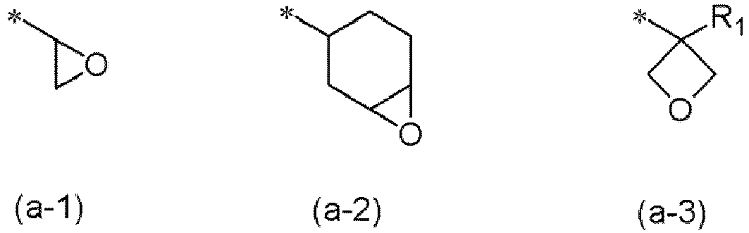
- In the formulae, R1 represents a hydrogen atom or an organic group having 1 to 10 carbon atoms, and "*" represents an attachment point.
- When such a heterocyclic structure is contained, the epoxy or oxetane structure undergoes a ring-opening reaction during heating for film formation, and thus, the film is cured. Moreover, the hydroxy groups generated by this ring-opening reaction also contribute to improvement in adhesiveness to a resist upper layer film.
- The R1 in the formula (a-3) represents a hydrogen atom or an organic group having 1 to 10 carbon atoms, preferably a hydrogen atom, a methyl group, or an ethyl group, more preferably an ethyl group.
- The ligand is preferably derived from a structure represented by the following general formula (1) or (2).
RaXOH (1)
RaXCOOH (2)
- In the formulae, Ra represents a group represented by any of the formulae (a-1) to (a-3); and X represents a divalent organic group having 1 to 20 carbon atoms.
- The X in the formulae represents a divalent organic group having 1 to 20 carbon atoms, and may contain one or more kinds selected from an oxygen atom, a nitrogen atom, and a sulfur atom.
- It is preferable for the ligand contained in the compound for forming a metal-containing film to be a ligand derived from the above-described structures from the viewpoint of the productivity of the compound for forming a metal-containing film. This is also favorable from the viewpoint of the availability of raw materials on providing a compound for forming a metal-containing film, having a ligand containing any of the groups represented by the formulae (a-1) to (a-3).
- Furthermore, it is preferable that the X is a hydrocarbon group having 1 to 10 carbon atoms, the structure represented by the general formula (2) is a structure represented by the following general formula (x-1) or (x-2), or the structure represented by the general formula (1) is a structure represented by the following formula (x-3).


- In the formulae, Y1 to Y3 each represent a divalent organic group having 1 to 10 carbon atoms; Ra is as defined above; "n" represents 0 or 1; and "m" represents 0 or 1.

- In the formula, Y4 represents a divalent organic group having 1 to 10 carbon atoms; Ra is as defined above; and "l" represents 0 or 1.
- The Y1 to Y4 are more preferably each a divalent hydrocarbon group having 1 to 10 carbon atoms from the viewpoint of heat resistance.
- As specific examples of the structure represented by the general formula (x-1), the following structures are favorable.


- In the formulae, Ra is as defined above.
- As specific examples of the structures represented by the general formula (x-2), the following structures are favorable.


- In the formulae, Ra is as defined above, and Rx represents a hydrogen atom or a monovalent organic group having 1 to 10 carbon atoms.
- As specific examples of the structure represented by the general formula (x-3), the following structures are favorable.


- In the formulae, Ra is as defined above, and "m" represents 0 to 4.
- In the case of the general formula (x-2), Ra is more preferably a group represented by the formula (a-3) from the viewpoint of the availability of raw materials.
- The compound for forming a metal-containing film is preferably a reaction product of a reaction between: a metal compound represented by the following general formula (3) or a metal-containing compound containing a hydrolysate, condensate, or hydrolysis condensate of the metal compound represented by the following general formula (3); and the structure represented by the general formula (1) or (2).
LaMXb (3)
- In the formula, M represents any of Ti, Zr, and Hf, L represents a monodentate ligand having 1 to 30 carbon atoms or a polydentate ligand having 1 to 30 carbon atoms, X represents a hydrolysable group selected from a halogen atom, an alkoxy group, a carboxylate group, an acyloxy group, and -NR1R2, R1 and R2 each independently represent a hydrogen atom or a monovalent organic group having 1 to 20 carbon atoms, and a+b = 4, "a" and "b" each representing an integer of 0 to 4.
- Such a compound for forming a metal-containing film makes it possible to form a metal-containing film excellent in dry etching resistance to oxygen gas when the compound is contained in a composition for forming a metal-containing film.
- Examples of the hydrolysable group X of the general formula (3) include one or more selected from halogen atoms, alkoxy groups, carboxylate groups, acyloxy groups, and -NR1R2. R1 and R2 each independently represent a hydrogen atom or a monovalent organic group having 1 to 20 carbon atoms.
- Examples of the halogen atoms include a fluorine atom, a chlorine atom, a bromine atom, an iodine atom, etc.
- Examples of the alkoxy groups include a methoxy group, an ethoxy group, an n-propoxy group, an i-propoxy group, an n-butoxy group, a t-butoxy group, etc.
- Examples of the carboxylate groups include an acetate group, a propionate group, a butyrate group, an n-hexanecarboxylate group, an n-octanecarboxylate group, etc.
- Examples of the acyloxy groups include an acetoxy group, an ethylyloxy group, a propionyloxy group, a butyryloxy group, a t-butyryloxy group, a t-amylyloxy group, an n-hexanecarbonyloxy group, an n-octanecarbonyloxy group, etc.
- Examples of the -NR1R2 include an unsubstituted amino group, a methylamino group, a dimethylamino group, a diethylamino group, a dipropylamino group, etc.
- As the hydrolysable group X, an alkoxy group is preferable, and an i-propoxy group, an n-butoxy group, or a t-butoxy group is more preferable.
- Examples of the monodentate ligand include a hydroxo ligand, a carboxy ligand, an amido ligand, an amine ligand, an ammonia ligand, an olefin ligand, etc.
- Examples of the carboxy ligand include a formate ligand (OOCH), an acetate ligand (OOCMe), a propionate ligand (OOCEt), and a butyrate ligand (OOCPr).
- Examples of the amido ligand include an unsubstituted amido ligand (NH2), a methylamido ligand (NHMe), a dimethylamido ligand (NMe2), a diethylamido ligand (NEt2), a dipropylamido ligand (NPr2), etc.
- Examples of the amine ligand include pyridine, a trimethylamine ligand, a piperidine ligand, etc.
- Examples of the olefin ligand include: linear olefins, such as ethylene and propylene; cyclic olefins, such as cyclopentene, cyclohexene, and norbornene; etc.
- Examples of the polydentate ligand include a ligand derived from a hydroxy acid ester, a ligand derived from a β-diketone, a ligand derived from a β-keto ester, a ligand derived from an α,α-dicarboxylic acid ester, a hydrocarbon having a π bond, diphosphine, etc.
- Examples of the hydroxy acid ester include glycolic acid esters, lactic acid esters, 2-hydroxycyclohexane-1-carboxylic acid esters, salicylic acid esters, etc.
- Examples of the β-keto ester include acetoacetic acid esters, α-alkyl-substituted acetoacetic acid esters, β-ketopentanoic acid esters, benzoylacetic acid esters, 1,3-acetonedicarboxylic acid esters, etc.
- Examples of the β-diketone include acetylacetone, methylacetylacetone, and ethylacetylacetone.
- Examples of the α,α-dicarboxylic acid ester include malonic acid diesters, α-alkyl-substituted malonic acid diesters, α-cycloalkyl-substituted malonic acid diesters, α-aryl-substituted malonic acid diesters, etc.
- Examples of the hydrocarbon having a π bond include: chain dienes, such as butadiene and isoprene; cyclic dienes, such as cyclopentadiene, methylcyclopentadiene, pentamethylcyclopentadiene, cyclohexadiene, and norbornadiene; aromatic hydrocarbons, such as benzene, toluene, xylene, hexamethylbenzene, naphthalene, and indene; etc.
- Examples of the diphosphine include 1,1-bis(diphenylphosphino)methane, 1,2-bis(diphenylphosphino)ethane, 1,3-bis(diphenylphosphino)propane, 2,2'-bis(diphenylphosphino)-1,1'-binaphthyl, 1,1'-bis(diphenylphosphino)ferrocene, etc.
- In the general formula (3), a+b = 4, and "a" and "b" each represent an integer of 0 to 4. "a" is preferably 0 to 3, more preferably 0 to 2, further preferably 1 or 2, and particularly preferably 2. "b" is preferably 2 to 4, more preferably 2 or 3, and further preferably 2. By setting "a" and "b" to be within the above ranges, the stability of the compound for forming a metal-containing film can be enhanced.
- Examples of the metal compound and metal-containing compound (a) include: compounds containing titanium, such as diisopropoxybis(2,4-pentanedionate)titanium(IV), tetra-n-butoxytitanium(IV), tetra-n-propoxytitanium(IV), tri-n-butoxymonostearatetitanium(IV), titanium(IV)butoxide oligomer, aminopropyltrimethoxytitanium(IV), triethoxymono(2,4-pentanedionate)titanium(IV), tri-n-propoxymono(2,4-pentanedionate)titanium(IV), triisopropoxymono(2,4-pentanedionate)titanium, and di-n-butoxybis(2,4-pentanedionate)titanium(IV); compounds containing zirconium, such as dibutoxybis(ethylacetoacetate)zirconium(IV), di-n-butoxybis(2,4-pentanedionate)zirconium(IV), tetra-n-butoxyzirconium(IV), tetra-n-propoxyzirconium(IV), tetraisopropoxyzirconium(IV), aminopropyltriethoxyzirconium(IV), 2-(3,4-epoxycyclohexyl)ethyltrimethoxyzirconium(IV), γ-glycidoxypropyltrimethoxyzirconium(IV), 3-isocyanopropyltrimethoxyzirconium(IV), triethoxymono(2,4-pentanedionate)zirconium(IV), tri-n-propoxymono(2,4-pentanedionate)zirconium(IV), triisopropoxymono(2,4-pentanedionate)zirconium(IV), tri(3-methacryloxypropyl)methoxyzirconium(IV), and tri(3-acryloxypropyl)methoxyzirconium(IV); and compounds containing hafnium, such as diisopropoxybis(2,4-pentanedionate)hafnium(IV), tetrabutoxyhafnium(IV), tetraisopropoxyhafnium(IV), tetraethoxyhafnium(IV), and dichlorobis(cyclopentadienyl)hafnium(IV) .
- From the viewpoint of the availability of raw materials, the metal compound preferably has a structure represented by the following general formula (4).
M(OR1A)4 (4)
- In the formula, M is as defined above; and R1A represents a monovalent organic group having 1 to 20 carbon atoms.
- In the general formula (4), R1A represents a monovalent organic group having 1 to 20 carbon atoms, preferably a methyl group, an ethyl group, an n-propyl group, an i-propyl group, an n-butyl group, or a t-butyl group, and more preferably an isopropyl group, an n-butyl group, or a t-butyl group.
- At the time of the synthesis reaction of the compound for forming a metal-containing film, a compound that may become a monodentate ligand or a polydentate ligand (hereinafter, compound (b) for forming a ligand) in the compound for forming a metal-containing film can be contained besides the metal compound or metal-containing compound (a) and the structure including any of the groups represented by the formulae (a-1) to (a-3).
- Examples of the compound (b) for forming a ligand include compounds, such as organic compounds derived from a hydroxo ligand, a carboxy ligand, an amido ligand, an amine ligand, an ammonia ligand, an olefin ligand, etc. and organic compounds derived from a ligand derived from a hydroxy acid ester, a ligand derived from a β-diketone, a ligand derived from a β-keto ester, a ligand derived from an α,α-dicarboxylic acid ester, etc., given as examples of the L in the general formula (3). Examples also include compounds having multiple hydroxy groups etc.
- Furthermore, the compound (b) for forming a ligand may be an organic compound having 1 to 30 carbon atoms including at least one crosslinking group represented by any of the following general formulae (c-1) to (c-4), (d-1) to (d-4), and (e-1) to (e-3).


- In the formulae, Ye represents a divalent organic group having 1 to 20 carbon atoms; Re2 represents a hydrogen atom, a substituted or unsubstituted saturated divalent organic group having 1 to 20 carbon atoms, a substituted or unsubstituted unsaturated divalent organic group having 2 to 20 carbon atoms, a substituted or unsubstituted aryl group having 6 to 30 carbon atoms, or a substituted or unsubstituted arylalkyl group having 7 to 31 carbon atoms; Re1 represents an organic group whose protecting group is to be removed by an action of an acid, heat, or both to generate one or more hydroxy groups or carboxy groups, Re1 being represented by one of the following general formulae (e-4); and "*" represents an attachment point.

- In the formulae, Re3 represents an organic group whose protecting group is to be removed by an action of an acid, heat, or both; and "*" represents an attachment point to Ye.
- When the compound for forming a metal-containing film contains at least one crosslinking group represented by any of the general formulae (c-1) to (c-4), (d-1) to (d-4), and (e-1) to (e-3), sufficient thermal flowability can be achieved at the time of film formation, and therefore, when the compound is contained in a composition for forming a metal-containing film, it is possible to form a metal-containing film excellent in flatness.
- From the viewpoints of the productivity and stability of the compound for forming a metal-containing film, the compound (b) for forming a ligand is more preferably a compound derived from a carboxy ligand, a compound derived from a ligand derived from a β-diketone, or a compound having a plurality of hydroxy groups. One kind of these compounds may be used, or two or more kinds thereof may be used in combination.
- Examples of the compound derived from a carboxy ligand include compounds represented by the following general formula (5').

- In the formula, "p" represents 0 or 1. When "p" is 1, X1 represents a divalent organic group having 2 to 20 carbon atoms, and W represents an alkoxy group having 1 to 10 carbon atoms, the following general formula (5-A), or a crosslinking group represented by any of the general formulae (d-1) to (d-4). When "p" is 0, X1 represents a monovalent organic group having 8 to 30 carbon atoms including an aromatic ring and a crosslinking group of either of the structures represented by the general formulae (c-2) and (c-3).

- In the formula, Y represents a saturated organic group having a valency of h+1 and having 1 to 20 carbon atoms or an unsaturated organic group having a valency of h+1 and having 2 to 20 carbon atoms; RA represents any of the crosslinking groups represented by the general formulae (c-1) to (c-4); "h" represents 1 to 6; and "*" represents an attachment point to a carbon atom of a carbonyl group.
- A compound for forming a metal-containing film, containing a carboxy ligand having such a structure, can improve thermosetting property when a composition for forming a metal-containing film is formed, and makes it possible to form a metal-containing film excellent in resistance against mixing with a resist upper layer film.
- In the general formula (5'), it is preferable that "p" is 1 and W has a structure represented by the following general formula (5-B-1) or (5-B-2).

- In the formulae, RA1 represents a crosslinking group represented by the general formula (c-1); RA2 represents a crosslinking group represented by the general formula (c-2) or (c-3); Z represents an oxygen atom or a secondary amine; L1 represents a divalent hydrocarbon group having 1 to 10 carbon atoms; and RA3 represents a saturated monovalent organic group having 1 to 20 carbon atoms or an unsaturated monovalent organic group having 2 to 20 carbon atoms. "u" represents 0 or 1. When "u" is 0, "t" is 1 to 5 and "s" is 0 to 4, provided that t+s is 1 or more and 5 or less, and when "u" is 1, "t" is 1 to 6 and "s" is 0 to 5, provided that t+s is 1 or more and 6 or less. "r" represents 1 to 10; "m" represents 0 or 1; and "*" represents an attachment point to a carbon atom of a carbonyl group.
- A compound for forming a metal-containing film, containing a carboxy ligand having such a structure, can improve heat resistance when a composition for forming a metal-containing film is formed, and therefore, a formed metal-containing film exhibits excellent film-formability. It is also possible to suppress the generation of sublimation products during heat-curing and, therefore, to prevent the contamination of equipment.
- In the general formula (5'), it is preferable that "p" is 1, W is an alkoxy group having 1 to 10 carbon atoms, and X1 is any of the structures represented by the following general formulae (5-C).


- In the formulae, "*" represents an attachment point to a carbon atom of a carbonyl group.
- A compound for forming a metal-containing film, containing a carboxy ligand having such a structure, can improve heat resistance when a composition for forming a metal-containing film is formed, and therefore, a formed metal-containing film exhibits excellent film-formability. It is also possible to suppress the generation of sublimation products during heat-curing and, therefore, to prevent the contamination of equipment.
- Alternatively, in the general formula (5'), it is also preferable that "p" is 0, and X1 has one of the structures represented by the following formulae (5-D).

- In the formulae, Rf represents a hydrogen atom or a monovalent organic group having 1 to 10 carbon atoms; and "*" represents an attachment point to a carbon atom of a carbonyl group.
- Other examples of the compound derived from a carboxy ligand include compounds represented by the following general formula (6).

- In the formula, X2 represents a divalent organic group having 1 to 31 carbon atoms; and R6A represents any of the general formulae (e-1) to (e-3).
- In the general formula (6), X2 represents a divalent organic group having 1 to 31 carbon atoms, and in view of thermosetting property, preferably represents a saturated hydrocarbon group having 1 to 20 carbon atoms or an unsaturated hydrocarbon group having 2 to 20 carbon atoms.
- In the general formulae (e-1) to (e-3), Ye represents a substituted or unsubstituted saturated divalent organic group having 1 to 20 carbon atoms, a substituted or unsubstituted unsaturated divalent organic group having 2 to 20 carbon atoms, a substituted or unsubstituted aryl group having 6 to 30 carbon atoms, or a substituted or unsubstituted arylalkyl group having 7 to 31 carbon atoms, and Ye is preferably a saturated hydrocarbon group having 1 to 20 carbon atoms or an unsaturated hydrocarbon group having 2 to 20 carbon atoms.
- When the Ye in the general formulae (e-1) to (e-3) is a saturated hydrocarbon group having 1 to 20 carbon atoms or an unsaturated hydrocarbon group having 2 to 20 carbon atoms, the thermosetting property of a composition for forming a metal-containing film can be further improved when the composition is formed with the compound for forming a metal-containing film. This is also desirable from the viewpoint of the availability of raw materials.
- Specific examples of Ye include the following structures, but are not limited thereto.


- "*1" represents an attachment point to an oxygen atom or a nitrogen atom; and "*2" represents an attachment point to Re1.
- The Re3 in the general formula (e-4) represents an organic group whose protecting group is to be removed by an action of an acid, heat, or both, preferably represents a tertiary hydrocarbyl group, or a group that forms an acetal structure together with an adjacent oxygen atom, and particularly preferably represents a tertiary hydrocarbyl group. As the tertiary hydrocarbyl group, those having 4 to 20 carbon atoms are preferable, and in particular, those having fewer carbon atoms are more preferable.
- Examples of the compound derived from a ligand derived from a β-diketone include compounds represented by the following general formula (7).

- In the formula, R7A to R7c each represent a hydrogen atom or a monovalent organic group having 1 to 20 carbon atoms and optionally containing a crosslinking group represented by any of the general formulae (c-1) to (c-4) and (d-1) to (d-4).
- The compounds of the general formula (7) preferably contain at least one crosslinking group represented by any of the general formulae (c-1) to (c-4) and (d-1) to (d-4). Such a compound is capable of further improving the thermosetting property of a composition for forming a metal-containing film when the composition is formed with the compound for forming a metal-containing film, and is therefore preferable.
- Examples of the compound having multiple hydroxy groups include dihydric alcohols represented by any of the following general formulae (7-A) to (7-C) etc.

- In the formulae, R7a and R7b each represent a hydrogen atom or a monovalent organic group having 1 to 20 carbon atoms and optionally containing a crosslinking group represented by any of the general formulae (c-1) to (c-4); R7c to R7f each represent a hydrogen atom or a monovalent organic group having 1 to 20 carbon atoms and optionally containing a crosslinking group represented by any of the general formulae (c-1) to (c-4) and (d-1) to (d-4); and Y2 represents a divalent organic group having 1 to 10 carbon atoms. In the general formula (7-A), the adjacent R7a and R7b may be bonded to each other to form an unsaturated or saturated cyclic structure.
- The compounds of the general formulae (7-A) to (7-C) preferably contain at least one crosslinking group represented by any of the general formulae (c-1) to (c-4) and (d-1) to (d-4). Such a compound is capable of further improving the thermosetting property of a composition for forming a metal-containing film when the composition is formed with the compound for forming a metal-containing film, and is therefore preferable.
- In the compound for forming a metal-containing film, the ligand containing any of the groups represented by the formulae (a-1) to (a-3) is preferably contained in an amount of 10 mol% to 90 mol%, more preferably 20 mol% to 80 mol%, and further preferably 25 mol% to 75 mol% of the total amount of ligands coordinated to the metal atom. The ligand derived from the compound (b) for forming a ligand is preferably contained in an amount of 0 mol% to 50 mol%, more preferably 0 mol% to 30 mol% of the total amount of ligands coordinated to the metal atom. Ligands other than the ligand of the compound (b) for forming a ligand, for example, a ligand derived from an alkoxy group having 1 to 10 carbon atoms, are preferably contained in an amount of 0 mol% to 90 mol%, more preferably 20 mol% to 80 mol% of the total amount of ligands coordinated to the metal atom.
- Furthermore, on the occasion of the synthesis reaction of the compound for forming a metal-containing film, a silicon-containing compound (c) may be added besides the metal compound or metal-containing compound (a) and the structure including any of the groups represented by the formulae (a-1) to (a-3).
- By substituting a hydrolysable group of the metal compound or metal-containing compound (a) with the silicon-containing compound (c), it is possible to enhance the stability of the compound for forming a metal-containing film in the composition for forming a metal-containing film.
- That is, the compound for forming a metal-containing film preferably further contains a ligand derived from a silicon compound represented by the following general formula (5).

- In the formula, R3A, R3B, and R3C each represent any organic group selected from an organic group having 2 to 30 carbon atoms including a crosslinking group of a structure represented by any of the following general formulae (b-1) to (b-3), a substituted or unsubstituted alkyl group having 1 to 20 carbon atoms, and an aryl group having 6 to 20 carbon atoms.

- In the formulae, R3 represents a hydrogen atom or a monovalent organic group having 1 to 10 carbon atoms; "q" represents 0 or 1; and "*" represents an attachment point.
- As the silicon-containing compound, a compound of any of the following formulae is preferable, and from the viewpoint of productivity, trimethylsilanol is more preferable.

- When the compound for forming a metal-containing film contains the ligand containing any of the groups represented by the formulae (a-1) to (a-3) and the ligand derived from the silicon-containing compound (c), the amount of the ligand containing any of the groups represented by the formulae (a-1) to (a-3) contained in the compound for forming a metal-containing film is preferably 10 mol% to 90 mol%, more preferably 20 mol% to 80 mol%, and further preferably 25 mol% to 75 mol% of the total amount of ligands coordinated to the metal atom. The ligand derived from the silicon-containing compound (c) is preferably contained in an amount of 10 mol% to 90 mol%, more preferably 20 mol% to 80 mol% of the total amount of ligands coordinated to the metal atom. Ligands other than the ligand containing any of the groups represented by the formulae (a-1) to (a-3) and the ligand derived from the silicon-containing compound (c), for example, a ligand derived from an alkoxy group having 1 to 10 carbon atoms, are preferably contained in an amount of 0 mol% to 90 mol%, more preferably 20 mol% to 80 mol% of the total amount of ligands coordinated to the metal atom.
- In addition, the present invention provides a method for manufacturing a compound for forming a metal-containing film, the method including performing a reaction between: a metal compound containing at least one metal atom selected from the group consisting of Ti, Zr, and Hf; and a ligand containing a group represented by any of the formulae (a-1) to (a-3).
- In this event, a ligand having a structure represented by the general formula (1) or (2) is preferably used as the ligand.
- Furthermore, as the ligand, it is preferable to use a ligand in which the X is a hydrocarbon group having 1 to 10 carbon atoms, the structure represented by the general formula (2) is a structure represented by the general formula (x-1) or (x-2), or the structure represented by the general formula (1) is a structure represented by the formula (x-3).
- In this event, the Y1 to Y4 are preferably each a divalent hydrocarbon group having 1 to 10 carbon atoms.
- Furthermore, as the compound for forming a metal-containing film, it is preferable to use a reaction product of a reaction between: a metal compound represented by the general formula (3) or a metal-containing compound containing a hydrolysate, condensate, or hydrolysis condensate of the metal compound represented by the general formula (3); and the structure represented by the general formula (1) or (2).
- In this event, as the metal compound, it is preferable to use a metal compound having a structure represented by the general formula (4).
- The metal compound used in the present invention is not particularly limited as long as the metal compound contains at least one kind of metal atom selected from the group consisting of Ti, Zr, and Hf.
- When a compound for forming a metal-containing film, containing a ligand containing any of the groups represented by the formulae (a-1) to (a-3), is to be synthesized, the synthesis method is not particularly limited as long as the compound for forming a metal-containing film contains the ligand containing any of the groups represented by the formulae (a-1) to (a-3). For example, a metal alkoxide or a metal acetylacetonate (acac) can be used as the metal compound or metal-containing compound (a), and the compound for forming a metal-containing film can be obtained by allowing the metal alkoxide or metal acac to react with the ligand containing any of the groups represented by the formulae (a-1) to (a-3). The metal compound (a) may be subjected to hydrolysis condensation and then the product may be allowed to react with the ligand containing any of the groups represented by the formulae (a-1) to (a-3), or the metal compound (a) may be allowed to react with the ligand containing any of the groups represented by the formulae (a-1) to (a-3) and then the product may be subjected to hydrolysis condensation. If it is difficult to control the hydrolysis condensation, the reaction with the ligand containing any of the groups represented by the formulae (a-1) to (a-3) may be performed in a non-hydrous environment. The method is preferably adjusted appropriately in accordance with the properties required in the compound for forming a metal-containing film and the metal-containing film. When the ligand derived from the silicon-containing compound (c) and the ligand containing any of the groups represented by the formulae (a-1) to (a-3) are to be contained as ligands, it is preferable to allow the metal compound or metal-containing compound (a) and the silicon-containing compound (c) to react and then allow the product to react with the ligand containing any of the groups represented by the formulae (a-1) to (a-3).
- As a method for performing a hydrolysis condensation reaction using the metal compound (a), examples include a method of subjecting the metal compound (a) to a hydrolysis condensation reaction in a solvent containing water. In this case, another compound having a hydrolysable group may be added as necessary. In addition, as a catalyst for the hydrolysis condensation reaction, an acid, such as acetic acid, may be added. The lower limit of the amount of water used in this hydrolysis condensation reaction is preferably 0.2-fold, more preferably 1-fold, and further preferably 3-fold, relative to the hydrolysable groups contained in the metal compound (a) etc., on the molar basis. The upper limit of the amount of the water is preferably 20-fold, more preferably 15-fold, and further preferably 10-fold on the molar basis.
- The solvent used in the synthesis reaction of the compound for forming a metal-containing film is not particularly limited, and for example, a solvent given as an example of the organic solvent (B) described later can be used. Typical solvents and solvent mixtures contain an ester, ether, or alcohol functional group, and examples thereof include a mixture of propylene glycol monomethyl ether acetate (PGMEA) and propylene glycol monomethyl ether (PGME) at a ratio of 70/30 by volume. Examples of other solvents that can be used include butanediol monomethyl ether, ethylene glycol monomethyl ether, butanediol monoethyl ether, propylene glycol monoethyl ether, ethylene glycol monoethyl ether, butanediol monopropyl ether, propylene glycol monopropyl ether, ethylene glycol monopropyl ether, ethylene glycol monobutyl ether, diethylene glycol monomethyl ether, diethylene glycol monoethyl ether, diethylene glycol monopropyl ether, diethylene glycol monobutyl ether, propylene glycol monobutyl ether, 1-butanol, 2-butanol, 2-methyl-1-propanol, 4-methyl-2-pentanol, acetone, tetrahydrofuran, toluene, hexane, ethyl acetate, cyclohexanone, methyl amyl ketone, propylene glycol dimethyl ether, diethylene glycol dimethyl ether, diamyl ether, isoamyl ether, propylene glycol monomethyl ether acetate, propylene glycol monoethyl ether acetate, ethyl pyruvate, butyl acetate, methyl 3-methoxypropionate, ethyl 3-ethoxypropionate, t-butyl acetate, t-butyl propionate, propylene glycol mono-t-butyl ether acetate, γ-butyrolactone, methyl isobutyl ketone, cyclopentyl methyl ether, etc.
- In addition, the present invention provides a composition for forming a metal-containing film, containing: (A) the above-described compound for forming a metal-containing film; and (B) an organic solvent.
- In this case, the composition for forming a metal-containing film preferably contains one or more of (C) a thermal acid generator and (D) a photo-acid generator, and the composition for forming a metal-containing film preferably further contains one or more of (E) a crosslinking agent and (G) a surfactant.
- In the following, each of the components contained in the inventive composition for forming a metal-containing film will be described in detail.
- The organic solvent (B) usable in the inventive composition for forming a metal-containing film is not particularly limited as long as the organic solvent is capable of dissolving or dispersing the compound (A) for forming a metal-containing film, and when contained, (C) a thermal acid generator, (D) a photo-acid generator, (E) a crosslinking agent, (G) a surfactant, other additives, etc. described later.
- Specifically, for example, an organic solvent disclosed in paragraphs [0091] and [0092] in
JP2007-199653A - The organic solvent (B) is preferably contained in an amount of 200 to 10,000 parts by mass, more preferably 250 to 5,000 parts by mass relative to 100 parts by mass of the compound (A) for forming a metal-containing film.
- Furthermore, the organic solvent (B) may be a mixture of one or more organic solvents having a boiling point of lower than 180°C and one or more organic solvents having a boiling point of 180°C or higher. In the present invention, an organic solvent having a boiling point of 180°C or higher is also referred to as a high-boiling-point organic solvent. Note that, the boiling point is a boiling point at normal pressure.
- The high-boiling-point organic solvent is not particularly limited to hydrocarbons, alcohols, ketones, esters, ethers, or chlorine-based solvents, as long as the solvent is capable of dissolving or dispersing the components of the inventive composition for forming a metal-containing film. Specific examples include 1-octanol, 2-ethylhexanol, 1-nonanol, 1-decanol, 1-undecanol, ethylene glycol, 1,2-propylene glycol, 1,3-butylene glycol, 2,4-pentanediol, 2-methyl-2,4-pentanediol, 2,5-hexanediol, 2,4-heptanediol, 2-ethyl-1,3-hexanediol, diethylene glycol, dipropylene glycol, triethylene glycol, tripropylene glycol, glycerin, n-nonyl acetate, monohexyl ether, ethylene glycol mono-2-ethylhexyl ether, ethylene glycol monophenyl ether, ethylene glycol monobenzyl ether, diethylene glycol monoethyl ether, diethylene glycol monoisopropyl ether, diethylene glycol mono-n-butyl ether, diethylene glycol monoisobutyl ether, diethylene glycol monohexyl ether, diethylene glycol monophenyl ether, diethylene glycol monobenzyl ether, diethylene glycol diethyl ether, diethylene glycol dibutyl ether, diethylene glycol butyl methyl ether, triethylene glycol dimethyl ether, triethylene glycol monomethyl ether, triethylene glycol-n-butyl ether, triethylene glycol butyl methyl ether, tetraethylene glycol dimethyl ether, dipropylene glycol monomethyl ether, dipropylene glycol mono-n-propyl ether, dipropylene glycol mono-n-butyl ether, tripropylene glycol dimethyl ether, tripropylene glycol monomethyl ether, tripropylene glycol mono-n-propyl ether, tripropylene glycol mono-n-butyl ether, ethylene glycol monoethyl ether acetate, ethylene glycol monobutyl ether acetate, diethylene glycol monomethyl ether acetate, diethylene glycol monoethyl ether acetate, diethylene glycol monobutyl ether acetate, triacetin, propylene glycol diacetate, dipropylene glycol methyl-n-propyl ether, dipropylene glycol methyl ether acetate, 1,4-butanediol diacetate, 1,3-butylene glycol diacetate, 1,6-hexanediol diacetate, triethylene glycol diacetate, γ-butyrolactone, methyl benzoate, ethyl benzoate, propyl benzoate, butyl benzoate, dihexyl malonate, diethyl succinate, dipropyl succinate, dibutyl succinate, dihexyl succinate, dimethyl adipate, diethyl adipate, dibutyl adipate, and the like. One of the solvents may be used or a mixture of two or more kinds may be used.
- The high-boiling-point organic solvent may be selected suitably from the solvents above, for example, depending on the temperature at which the inventive composition for forming a metal-containing film is heat-treated, etc. The boiling point of the high-boiling-point organic solvent is preferably 180°C to 300°C, further preferably 200°C to 300°C. When the boiling point is as described, the evaporation rate at the baking (heating) is appropriate, and therefore, it is possible to suppress the generation of dryness-induced defects at the time of film formation. Moreover, a solvent having such a boiling point evaporates after the baking and does not remain in the film. Therefore, the solvent does not affect the physical properties, such as etching resistance, of the film.
- Furthermore, when the high-boiling-point organic solvent is used, the contained amount is preferably 1 to 30 parts by mass per 100 parts by mass of the organic solvent having a boiling point lower than 180°C. When the contained amount is as described, sufficient thermal flowability can be imparted at the time of baking and the solvent does not remain in the film and cause degradation in the physical properties, such as etching resistance, of the film. Therefore, such an amount is preferable.
- In the inventive composition for forming a metal-containing film, a thermal acid generator (C) is preferably contained to promote a crosslinking reaction by heat.
- Examples of a thermal acid generator (C) usable in the inventive composition for forming a metal-containing film include the following general formula (7') etc.

- In the formula, XA - represents a non-nucleophilic counter ion. R70, R71, R72, and R73 each represent a hydrogen atom, a linear, branched, or cyclic alkyl group, alkenyl group, oxoalkyl group, or oxoalkenyl group, having 1 to 12 carbon atoms, an aryl group having 6 to 20 carbon atoms, or an aralkyl group or aryloxoalkyl group having 7 to 12 carbon atoms, part or all of the hydrogen atoms of these groups optionally being substituted with an alkoxy group or the like. In addition, R70 and R71, or R70, R71, and R72 optionally form a ring, and in a case where a ring is formed, R70 and R71, or R70, R71, and R72 represent an alkylene group having 3 to 10 carbon atoms, or a heteroaromatic ring having the nitrogen atom in the formula in the ring.
- The R70, R71, R72, and R73 may be identical to or different from each other, and specific examples of the alkyl group include a methyl group, an ethyl group, a propyl group, an isopropyl group, an n-butyl group, a sec-butyl group, a tert-butyl group, a pentyl group, a hexyl group, a heptyl group, an octyl group, a cyclopentyl group, a cyclohexyl group, a cycloheptyl group, a cyclopropylmethyl group, a 4-methylcyclohexyl group, a cyclohexylmethyl group, a norbornyl group, an adamantyl group, etc.
- Examples of the alkenyl group include a vinyl group, an allyl group, a propenyl group, a butenyl group, a hexenyl group, a cyclohexenyl group, etc.
- Examples of the oxoalkyl group include a 2-oxocyclopentyl group, a 2-oxocyclohexyl group, a 2-oxopropyl group, a 2-cyclopentyl-2-oxoethyl group, a 2-cyclohexyl-2-oxoethyl group, a 2-(4-methylcyclohexyl)-2-oxoethyl group, etc.
- Examples of the oxoalkenyl group include a 2-oxo-4-cyclohexenyl group, a 2-oxo-4-propenyl group, etc.
- Examples of the aryl group include a phenyl group; a naphthyl group; alkoxyphenyl groups, such as a p-methoxyphenyl group, an m-methoxyphenyl group, an o-methoxyphenyl group, an ethoxyphenyl group, a p-tert-butoxyphenyl group, and an m-tert-butoxyphenyl group; alkyl phenyl groups, such as a 2-methylphenyl group, a 3-methylphenyl group, a 4-methylphenyl group, an ethylphenyl group, a 4-tert-butylphenyl group, a 4-butylphenyl group, and a dimethylphenyl group; alkylnaphthyl groups, such as a methylnaphthyl group and an ethylnaphthyl group; alkoxynaphthyl groups, such as a methoxynaphthyl group and an ethoxynaphthyl group; dialkylnaphthyl groups, such as a dimethylnaphthyl group and a diethylnaphthyl group; dialkoxynaphthyl groups, such as a dimethoxynaphthyl group and a diethoxynaphthyl group; etc.
- Examples of the aralkyl group include a benzyl group, a phenylethyl group, a phenethyl group, etc.
- Examples of the aryloxoalkyl group include 2-aryl-2-oxoethyl groups such as a 2-phenyl-2-oxoethyl group, a 2-(1-naphthyl)-2-oxoethyl group, a 2-(2-naphthyl)-2-oxoethyl group, etc.
- When R70 and R71, or R70, R71, and R72 form a heteroaromatic ring having, in the ring, the nitrogen atom in the formula, examples include imidazole derivatives (for example, imidazole, 4-methylimidazole, 4-methyl-2-phenylimidazole, etc.), pyrazole derivatives, furazan derivatives, pyrroline derivatives (for example, pyrroline, 2-methyl-1-pyrroline, etc.), pyrrolidine derivatives (for example, pyrrolidine, N-methylpyrrolidine, pyrrolidinone, N-methylpyrrolidone, etc.), imidazoline derivatives, imidazolidine derivatives, pyridine derivatives (for example, pyridine, methylpyridine, ethylpyridine, propylpyridine, butylpyridine, 4-(1-butylpentyl)pyridine, dimethylpyridine, trimethylpyridine, triethylpyridine, phenylpyridine, 3-methyl-2-phenylpyridine, 4-tert-butylpyridine, diphenylpyridine, benzylpyridine, methoxypyridine, butoxypyridine, dimethoxypyridine, 4-pyrrolidinopyridine, 1-methyl-4-phenylpyridine, 2-(1-ethylpropyl)pyridine, aminopyridine, dimethylaminopyridine, etc.), pyridazine derivatives, pyrimidine derivatives, pyrazine derivatives, pyrazoline derivatives, pyrazolidine derivatives, piperidine derivatives, piperazine derivatives, morpholine derivatives, indole derivatives, isoindole derivatives, 1H-indazole derivatives, indoline derivatives, quinoline derivatives (for example, quinoline, 3-quinolinecarbonitrile, etc.), isoquinoline derivatives, cinnoline derivatives, quinazoline derivatives, quinoxaline derivatives, phthalazine derivatives, purine derivatives, pteridine derivatives, carbazole derivatives, phenanthridine derivatives, acridine derivatives, phenazine derivatives, 1,10-phenanthroline derivatives, adenine derivatives, adenosine derivatives, guanine derivatives, guanosine derivatives, uracil derivatives, uridine derivatives, etc.
- Examples of the non-nucleophilic counter ion of XA -include halide ions, such as chloride ion and bromide ion; fluoroalkylsulfonates, such as triflate, 1,1,1-trifluoroethanesulfonate, and nonafluorobutanesulfonate; arylsulfonates, such as tosylate, benzenesulfonate, 4-fluorobenzenesulfonate, and 1,2,3,4,5-pentafluorobenzenesulfonate; alkylsulfonates, such as mesylate and butanesulfonate; imidic acids, such as bis(trifluoromethylsulfonyl)imide, bis(perfluoroethylsulfonyl)imide, and bis(perfluorobutylsulfonyl)imide; methide acids, such as tris(trifluoromethylsulfonyl)methide and tris(perfluoroethylsulfonyl)methide; furthermore, sulfonates, represented by the following general formula (8), being fluorinated in the α-position; and sulfonates, represented by the following general formula (9), being fluorinated in the α- and β-positions.

R91CF2CF2SO3 - (9)
- In the general formula (8), R81 represents a hydrogen atom, a linear, branched, or cyclic alkyl group or acyl group having 1 to 23 carbon atoms, an alkenyl group having 2 to 20 carbon atoms, or an aryl group or aryloxy group having 6 to 20 carbon atoms. In the general formula (9), R91 represents a hydrogen atom, a linear, branched, or cyclic alkyl group having 1 to 20 carbon atoms, an alkenyl group having 2 to 20 carbon atoms, or an aryl group having 6 to 20 carbon atoms.
- Specific examples of the thermal acid generator include the following, but are not limited thereto.
- (CH3CH2)5N+H (CH3CH2)3N+H (CH3CH2)3N+H (CH3CH2)3N+H (CH3CH2)5N+H C4F9SO3 -


- One kind of the thermal acid generator (C), contained in the inventive composition for forming a metal-containing film, may be used, or two or more kinds thereof may be used in combination. The thermal acid generator (C) is preferably contained in an amount of 0.05 to 30 parts by mass, more preferably 0.1 to 10 parts by mass based on 100 parts by mass of the compound (A) for forming a metal-containing film. When the amount is 0.05 parts by mass or more, the amount of generated acid and crosslinking reaction are sufficient, and when 30 parts by mass or less, a mixing phenomenon due to an acid moving to an upper layer resist does not occur.
- The inventive composition for forming a metal-containing film can contain a photo-acid generator (D) for adjusting appropriately a pattern profile in a resist upper layer film, exposure sensitivity, etc. One kind of the photo-acid generator (D) may be used, or two or more kinds thereof may be used in combination. As the photo-acid generator (D), for example, those disclosed in paragraphs [0160] to [0179] of
JP2009-126940A - The inventive composition for forming a metal-containing film can also contain a crosslinking agent (E) to increase curability and further inhibit intermixing with a resist upper layer film. The crosslinking agent (E) is not particularly limited, and various known crosslinking agents can be widely used. Examples include melamine-based crosslinking agents, glycoluril-based crosslinking agents, benzoguanamine-based crosslinking agents, urea-based crosslinking agents, β-hydroxyalkylamide-based crosslinking agents, isocyanurate-based crosslinking agents, aziridine-based crosslinking agents, oxazoline-based crosslinking agents, epoxy-based crosslinking agents, and phenol-based crosslinking agents. One kind of the crosslinking agent (E) can be used, or two or more kinds thereof can be used in combination, and when the crosslinking agent (E) is contained, the contained amount is preferably 5 to 50 parts by mass, more preferably 10 to 40 parts by mass based on 100 parts by mass of the compound (A) for forming a metal-containing film. When the contained amount is 5 parts by mass or more, sufficient curability can be exhibited, and intermixing with a resist upper layer film can be suppressed. Meanwhile, when the contained amount is 50 parts by mass or less, there is no risk of degradation in dry etching resistance due to the proportion of the compound (A) for forming a metal-containing film in the composition being low.
- Specific examples of the melamine-based crosslinking agents include hexamethoxymethylated melamine, hexabutoxymethylated melamine, alkoxy- and/or hydroxy-substituted derivatives thereof, and partial self-condensates thereof.
- Specific examples of the glycoluril-based crosslinking agents include tetramethoxymethylated glycoluril, tetrabutoxymethylated glycoluril, alkoxy- and/or hydroxy-substituted derivatives thereof, and partial self-condensates thereof.
- Specific examples of the benzoguanamine-based crosslinking agents include tetramethoxymethylated benzoguanamine, tetrabutoxymethylated benzoguanamine, alkoxy- and/or hydroxy-substituted derivatives thereof, and partial self-condensates thereof.
- Specific examples of the urea-based crosslinking agents include dimethoxymethylated dimethoxyethyleneurea, alkoxy- and/or hydroxy-substituted derivatives thereof, and partial self-condensates thereof.
- Specific examples of the β-hydroxyalkylamide-based crosslinking agent include N,N,N',N'-tetra(2-hydroxyethyl)adipic acid amide.
- Specific examples of the isocyanurate-based crosslinking agents include triglycidyl isocyanurate and triallyl isocyanurate.
- Specific examples of the aziridine-based crosslinking agents include 4,4'-bis(ethyleneiminocarbonylamino)diphenylmethane and 2,2-bishydroxymethylbutanol-tris[3-(1-aziridinyl)propionate].
- Specific examples of the oxazoline-based crosslinking agents include 2,2'-isopropylidene bis(4-benzyl-2-oxazoline), 2,2'-isopropylidene bis(4-phenyl-2-oxazoline), 2,2'-methylene bis(4,5-diphenyl-2-oxazoline), 2,2'-methylene bis(4-phenyl-2-oxazoline), 2,2'-methylene bis(4-tert-butyl-2-oxazoline), 2,2'-bis(2-oxazoline), 1,3-phenylene bis(2-oxazoline), 1,4-phenylene bis(2-oxazoline), and a 2-isopropenyloxazoline copolymer.
- Specific examples of the epoxy-based crosslinking agents include diglycidyl ether, ethylene glycol diglycidyl ether, 1,4-butanediol diglycidyl ether, 1,4-cyclohexane dimethanol diglycidyl ether, poly(glycidyl methacrylate), trimethylolethane triglycidyl ether, trimethylolpropane triglycidyl ether, and pentaerythritol tetraglycidyl ether.
- Specific examples of the phenol-based crosslinking agents include compounds represented by the following general formula (10).

- In the formula, Q represents a single bond or a q1-valent hydrocarbon group having 1 to 20 carbon atoms. R16 represents a hydrogen atom or an alkyl group having 1 to 20 carbon atoms. "q1" represents an integer of 1 to 5.
- Q represents a single bond or a q1-valent hydrocarbon group having 1 to 20 carbon atoms. "q1" represents an integer of 1 to 5, more preferably 2 or 3. Specific examples of Q include groups obtained by removing "q1" hydrogen atoms from methane, ethane, propane, butane, isobutane, pentane, cyclopentane, hexane, cyclohexane, methylpentane, methylcyclohexane, dimethylcyclohexane, trimethylcyclohexane, benzene, toluene, xylene, ethylbenzene, ethylisopropylbenzene, diisopropylbenzene, methylnaphthalene, ethylnaphthalene, and eicosane. R16 represents a hydrogen atom or an alkyl group having 1 to 20 carbon atoms. Specific examples of the alkyl group having 1 to 20 carbon atoms include a methyl group, an ethyl group, a propyl group, an isopropyl group, a butyl group, an isobutyl group, a pentyl group, an isopentyl group, a hexyl group, an octyl group, an ethylhexyl group, a decyl group, and an eicosanyl group. A hydrogen atom or a methyl group is preferable.
- Specific examples of the compounds represented by the general formula (10) include the following compounds. Among these, a hexamethoxymethylated derivative of triphenolmethane, triphenolethane, 1,1,1,-tris(4-hydroxyphenyl)ethane, and tris(4-hydroxyphenyl)-1-ethyl-4-isopropylbenzene are preferable from the viewpoint of improving the curability and film thickness uniformity of the metal-containing film.


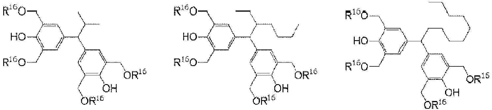


- A surfactant (G) may be contained in the inventive composition for forming a metal-containing film in order to improve coating property in spin-coating. One surfactant (G) can be used, or two or more surfactants (G) can be used in combination. Examples of the surfactant (G) include those disclosed in paragraphs [0142] to [0147] of
JP2009-269953A - The inventive composition for forming a metal-containing film can also contain a plasticizer. The plasticizer is not particularly limited, and various known plasticizers can be widely used. Examples include: low molecular-weight compounds, such as phthalate esters, adipate esters, phosphate esters, trimellitate esters, and citrate esters; and polymers, such as polyether polymers, polyester polymers, and polyacetal polymers described in
JP2013-253227A - In the present invention, by using the above-described composition for forming a metal-containing film, it is possible to form, for example, a metal-containing film as a resist underlayer film of a multilayer resist film used in lithography.
- In the method for forming a metal-containing film by using the inventive composition for forming a metal-containing film, a substrate to be processed is coated with the above-described composition for forming a metal-containing film by a spin-coating method or the like. After spin-coating, baking (heating) is performed so as to evaporate the solvent and promote a crosslinking reaction to prevent mixing with a resist upper layer film. The baking is preferably performed at a temperature of 100°C or higher and 450°C or lower for 10 to 600 seconds, more preferably at 200°C or higher and 300°C or lower for 10 to 300 seconds. In consideration of influences on device damage, wafer deformation, and the like, the upper limit of the heating temperature in the wafer process of lithography is preferably not more than 450°C, and more preferably not more than 300°C.
- In the method for forming a metal-containing film where the inventive composition for forming a metal-containing film is used, a substrate to be processed may also be coated with the inventive composition for forming a metal-containing film by spin-coating or the like in the same manner as described above, and then the composition for forming a metal-containing film may be baked and cured under an atmosphere having an oxygen concentration of 0.1 volume % or more and 21 volume % or less to form a metal-containing film.
- By virtue of baking the inventive composition for forming a metal-containing film in such an oxygen atmosphere, a sufficiently cured metal-containing film can be obtained. The atmosphere during baking may be air; however, to prevent oxidation of the metal-containing film, it is preferable to enclose an inert gas, such as N2, Ar, or He, therein to reduce the amount of oxygen. Control of oxygen concentration is necessary to prevent oxidation; the oxygen concentration is preferably 1,000 ppm or less, more preferably 100 ppm or less (volumetric basis). By thus preventing oxidation of the metal-containing film during the baking, the absorption does not increase and the etching resistance does not decrease, which is preferable.
- Alternatively, using the above-described composition for forming a metal-containing film, it is also possible to form, for example, a metal-containing film as a resist middle layer film of a multilayer resist film used in lithography.
- The present invention provides, as a patterning process according to a two-layer resist process using the inventive composition for forming a metal-containing film, a patterning process for forming a pattern in a substrate to be processed, including the steps of:
- (I-1) applying the above-described composition for forming a metal-containing film onto a substrate to be processed, followed by heating to form a metal-containing film;
- (I-2) forming a resist upper layer film on the metal-containing film by using a photoresist material;
- (I-3) subjecting the resist upper layer film to pattern exposure and then development with a developer to form a pattern in the resist upper layer film;
- (I-4) transferring the pattern to the metal-containing film by dry etching while using the resist upper layer film having the formed pattern as a mask; and
- (I-5) processing the substrate to be processed while using the metal-containing film having the transferred pattern as a mask to form the pattern in the substrate to be processed.
- The resist upper layer film in the two-layer resist process described above exhibits etching resistance with respect to chlorine-based gas. Therefore, the dry etching of the metal-containing film that is performed while using the resist upper layer film as a mask in the two-layer resist process is preferably performed using an etching gas mainly containing a chlorine-based gas. The metal-containing film exhibits etching resistance with respect to fluorine-based gas. Therefore, the dry etching of the substrate to be processed that is performed while using the metal-containing film as a mask is preferably performed using an etching gas mainly containing a fluorine-based gas.
- The present invention also provides, as a patterning process according to a three-layer resist process using the inventive composition for forming a metal-containing film, a patterning process for forming a pattern in a substrate to be processed, including the steps of:
- (II-1) forming a resist underlayer film on a substrate to be processed;
- (II-2) applying the above-described composition for forming a metal-containing film onto the resist underlayer film, followed by heating to form a metal-containing film;
- (II-3) forming a resist upper layer film on the metal-containing film by using a photoresist material;
- (II-4) subjecting the resist upper layer film to pattern exposure and then development with a developer to form a pattern in the resist upper layer film;
- (II-5) transferring the pattern to the metal-containing film by dry etching while using the resist upper layer film having the formed pattern as a mask;
- (II-6) transferring the pattern to the resist underlayer film by dry etching while using the metal-containing film having the transferred pattern as a mask; and
- (II-7) processing the substrate to be processed while using the resist underlayer film having the transferred pattern as a mask to form the pattern in the substrate to be processed.
- The metal-containing film, formed with the inventive composition for forming a metal-containing film, used as the resist middle layer film in the above-described three-layer resist process exhibits etching resistance with respect to oxygen-based gas. Therefore, the dry etching of the resist underlayer film that is performed while using the metal-containing film as a mask in the three-layer resist process is preferably performed using an etching gas mainly containing an oxygen-based gas. The resist underlayer film exhibits etching resistance with respect to fluorine-based gas. Therefore, the dry etching of the substrate to be processed that is performed while using the resist underlayer film as a mask is preferably performed using an etching gas mainly containing a fluorine-based gas.
- In the above-described patterning process, the resist upper layer film may be either a positive type or a negative type, and it is possible to use a composition similar to the typically used photoresist composition. In a case where the resist upper layer film is formed with the photoresist composition, a spin-coating method is preferable.
- In a case where the resist upper layer film is formed by a spin-coating method using a photoresist composition, prebaking is conducted after applying the photoresist composition. The prebaking is preferably performed at 60 to 180°C for 10 to 300 seconds. Thereafter, exposure is conducted according to a usual manner, followed by post-exposure baking (PEB) and development, and thereby, a resist upper layer film pattern can be obtained. Although the thickness of the resist upper layer film is not particularly limited, the thickness is preferably 10 to 500 nm, particularly preferably 20 to 400 nm.
- Examples of the light for exposure include high-energy beams at wavelengths of 300 nm or less, specifically, far ultraviolet rays, KrF excimer laser beam (248 nm), ArF excimer laser beam (193 nm), F2 laser beam (157 nm), Kr2 laser beam (146 nm), Ar2 laser beam (126 nm), soft X-rays at 3 to 20 nm (EUV), electron beam (EB), ion beam, X-rays, and the like.
- As the method for forming a pattern in the resist upper layer film, it is preferable to use a patterning process using a photolithography with a wavelength of 5 nm or more and 300 nm or less, a direct drawing using an electron beam, nanoimprinting, or a combination thereof.
- The development method in the patterning process is preferably alkali development or development using an organic solvent.
- Next, etching is performed while using the obtained resist upper layer film pattern as a mask. For example, the etching of the metal-containing film in the two-layer resist process is performed by using a chlorine-based gas while using the resist upper layer film pattern as a mask. In this manner, a metal-containing film pattern is formed. Next, the substrate to be processed is etched while using the obtained metal-containing film pattern as a mask. The etching of a body to be processed may be performed according to a usual manner. For example, in the case of a body to be processed made of SiO2, SiN or silica-based low dielectric constant insulating film, the etching is performed mainly based on a fluorocarbon-based gas.
- The metal-containing film obtained by using the inventive composition for forming a metal-containing film is characterized by its excellent etching resistance at the time of etching of the body to be processed.
- As a resist underlayer film material that can be used for the above-described resist underlayer film, examples include materials already known as materials for an underlayer film for a three-layer resist method or a two-layer resist method using a silicon resist composition. Examples include resins and compositions disclosed in
JP2012-001687A JP2012-077295A JP2004-264710A JP2005-043471A JP2005-250434A JP2007-293294A JP2008-065303A JP2004-205685A JP2007-171895A JP2009-014816A JP2007-199653A JP2008-274250A JP2010-122656A JP2012-214720A JP2014-029435A WO2012/077640A1 ,WO2010/147155A1 ,WO2012/176767A1 ,JP2005-128509A JP2006-259249A JP2006-259482A JP2006-293298A JP2007-316282A JP2012-145897A JP2017-119671A JP2019-044022A - The resist underlayer film can be formed on the substrate to be processed, for example, by using a composition solution containing the above-described resist underlayer film material and by a spin-coating method or the like in the same manner as the photoresist composition. After forming the resist underlayer film by a spin-coating method or the like, it is desirable to bake the film in order to evaporate the organic solvent. The baking temperature is preferably 100 to 600°C, and the baking time is preferably 10 to 300 seconds.
- Instead of the resist underlayer film material, it is also possible to adopt an organic hard mask formed by a CVD method or an ALD method.
- In the case of the three-layer resist process, the dry etching of the metal-containing film is performed, for example, by using a chlorine-based gas while using the resist upper layer film pattern as a mask. In this manner, the metal-containing film pattern is formed. Next, the resist underlayer film is etched by using an oxygen-based gas while using the obtained metal-containing film pattern as a mask. In this manner, the resist underlayer film pattern is formed. Next, the substrate to be processed is etched while using the obtained resist underlayer film pattern as a mask.
- The metal-containing film obtained by using the inventive composition for forming a metal-containing film is characterized by its excellent etching resistance at the time of etching of the resist underlayer film.
- Examples of the body to be processed (substrate to be processed) include, but are not particularly limited to, substrates made of Si, α-Si, p-Si, SiO2, SiN, SiON, W, TiN, Al, etc., those in which the layers to be processed are formed on the substrate, and the like. Examples of the layers to be processed include various low-k films, such as those made of Si, SiO2, SiON, SiN, p-Si, α-Si, W, W-Si, Al, Cu, Al-Si, and the like; and stopper films therefor, which can each be typically formed into a thickness of 50 to 10,000 nm, particularly 100 to 5,000 nm. When the layer to be processed is formed, the substrate and the layer to be processed are made of different materials.
- Here, with reference to
FIG. 1 , an example of a patterning process according to the above-described three-layer resist process will be described. In this example, firstly, a resistunderlayer film 3 is formed on alayer 2 to be processed of a substrate to be processed, including asubstrate 1 and thelayer 2 to be processed thereon, by using a resist underlayer film material, a metal-containingfilm 4 is formed on the resistunderlayer film 3 by using the inventive composition for forming a metal-containing film, and a resist upper layer film 5 is formed on the metal-containingfilm 4 by using a photoresist material, as inFIG. 1 (A) . Subsequently, an exposure portion 6 of the resist upper layer film is subjected to pattern exposure as inFIG. 1 (B) . Then, development is performed with a developer to form a resist upperlayer film pattern 5a in the resist upper layer film as inFIG. 1 (C) . Next, the pattern is transferred to the metal-containing film by dry etching while using the resist upper layer film having the formed resist upperlayer film pattern 5a as a mask to obtain a metal-containingfilm pattern 4a as inFIG. 1 (D) . Subsequently, the pattern is transferred to the resist underlayer film by dry etching while using the metal-containing film having the formed metal-containingfilm pattern 4a as a mask to obtain a resist underlayer film pattern 3a as inFIG. 1 (E) . Then, thelayer 2 to be processed on thesubstrate 1 is processed while using the resist underlayer film having the formed pattern 3a as a mask to form apattern 2a in the substrate to be processed as inFIG. 1 (F) . - With reference to
FIG. 2 , an example of a patterning process according to the above-described two-layer resist process will be described. In this example, firstly, a metal-containingfilm 4 is formed on alayer 2 to be processed of a substrate to be processed, including asubstrate 1 and thelayer 2 to be processed thereon, by using the inventive composition for forming a metal-containing film, and a resist upper layer film 5 is formed on the metal-containingfilm 4 by using a photoresist material, as inFIG. 2 (G) . Subsequently, an exposure portion 6 of the resist upper layer film is subjected to pattern exposure as inFIG. 2 (H) . Then, development is performed with a developer to form a resist upperlayer film pattern 5a in the resist upper layer film as inFIG. 2 (I) . Next, the pattern is transferred to the metal-containing film by dry etching while using the resist upper layer film having the formedpattern 5a as a mask to obtain a metal-containingfilm pattern 4a as inFIG. 2 (J) . Then, thelayer 2 to be processed on thesubstrate 1 is processed while using the metal-containing film having the formed metal-containingfilm pattern 4a as a mask to form apattern 2a in the substrate to be processed as inFIG. 2 (K) . - The present invention is further specifically described below with reference to Synthesis Examples, Comparative Synthesis Examples, Examples, and Comparative Examples. However, the present invention is not limited to these Examples.
- In the following Synthesis Examples, the following organic group starting material group G ((G1) to (G10)) and silicon-containing organic group starting material group H ((H1) and (H2)) were used.
- The organic group starting material group G ((G1) to (G10)) and the silicon-containing organic group starting material group H ((H1) and (H2)) are shown below.


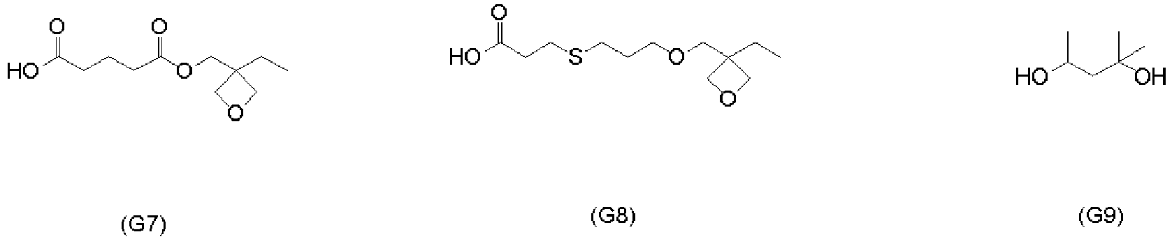


- As a metal source M, the following metal compounds were used.
- (M1): titanium tetraisopropoxide (377996 available from Sigma-Aldrich Corp)
- (M2): Hf(OBu)4: hafnium(IV) n-butoxide (667943 available from Sigma-Aldrich Corp)
- (M3): Zr(OBu)4: zirconium(IV) tetrabutoxide (80 mass% solution in 1-butanol) (Z0016 available from Tokyo Chemical Industry Co., Ltd.)
- Under a nitrogen atmosphere, 28.4 g of titanium tetraisopropoxide (M1) was dissolved in 50.0 g of 2-propanol, and while stirring, 50.0 g of a solution of 2.7 g of deionized water in IPA was added dropwise at room temperature over 2 hours. To the obtained solution, 10.0 g of the organic group starting material (G1) was added, and the mixture was agitated at room temperature for 30 minutes. After the solution was concentrated under reduced pressure at 30°C, it was further heated to 60°C and heating was continued under reduced pressure to generate no distillate. When distillates were no longer observed, 120.0 g of a PGMEA/PGME (ratio by mass: 70/30) solution was added thereto and heated under reduced pressure at 40°C until no IPA was distilled. Thus, a solution of a compound (A-1) for forming a metal-containing film in PGMEA/PGME was obtained.
- The compounds (A-2) to (A-8) for forming a metal-containing film shown in Table 1 were obtained under the same reaction conditions as in Synthesis Example 1, except that the metal source M and the organic group starting material group G were used at the charging amounts shown in Table 1.
[Table 1] Synthesis Example Metal source M Organic group starting material group G Compound Starting material g Starting material g 1 M1 28.4 G1 10.0 A-1 2 M2 47.9 G2 14.0 A-2 3 M3 48.5 G3 12.0 A-3 4 M3 47.9 G4 20.0 A-4 5 M3 47.9 G5 21.0 A-5 6 M3 47.9 G6 30.0 A-6 7 M3 47.9 G7 31.0 A-7 8 M3 47.9 G8 35.0 A-8 - Under a nitrogen atmosphere, 15.0 g of zirconium(IV) tetrabutoxide (M3) was dissolved in 20.6 g of a PGMEA/PGME (ratio by mass: 70/30) solution. The reaction temperature was raised to 50°C while stirring, and 9.0 g of the silicon-containing organic group starting material (H1) was added dropwise to the solution. After the addition, stirring was continued for 2 hours at a reaction temperature of 60°C. Subsequently, a mixture obtained by suspending 7.0 g of the organic group starting material (G3) in 8.6 g of a PGMEA/PGME (ratio by mass: 70/30) solution was added to the reaction system, and stirring was continued for 1 hour with the reaction temperature still at 60°C. After cooling to room temperature, the obtained reaction solution was filtered with a 0.45-µm PTFE filter. Thus, a solution of a compound (A-9) for forming a metal-containing film in PGMEA/PGME was obtained.
- The compounds (A-10) and (A-11) for forming a metal-containing film and the comparative compounds (R-1) and (R-2) shown in Table 2 were obtained under the same reaction conditions as in Synthesis Example 9, except that the metal source M, the organic group starting material group G, and the silicon-containing organic group starting material group H were used at the charging amounts shown in Table 2.
[Table 2] Synthesis Example Metal source M Organic group starting material group G Silicon-containing organic group starting material group H Compound Starting material g Starting material g Starting material g 9 M3 15.0 G3 7.0 H1 9.0 A-9 10 M3 15.0 G7 14.0 H2 9.0 A-10 11 M3 15.0 G8 16.0 H1 9.0 A-11 Comparative Synthesis Example 1 M3 15.0 G9 8.0 H1 9.0 R-1 Comparative Synthesis Example 2 M3 15.0 G10 6.0 H1 9.0 R-2 - For the preparation of compositions for forming a metal-containing film, the following were used: the compounds (A-1) to (A-11) for forming a metal-containing film and the comparative compounds (R-1) and (R-2); (AG1) as a thermal acid generator; (AG2) as a photo-acid generator; (XL1) and (XL2) as crosslinking agents; and (F1: ethylene glycol dibenzyl ether, having a boiling point of 364°C) as a high-boiling-point solvent. These were dissolved in an organic solvent containing 0.001 mass% of PF636 (available from OMNOVA Solutions Inc.) in proportions shown in Table 3, and then the solution was filtered through a 0.1-pm filter made of a fluororesin to prepare each of the compositions (MUL-1 to -16 and comparative MUL-1 and -2) for forming a metal-containing film.
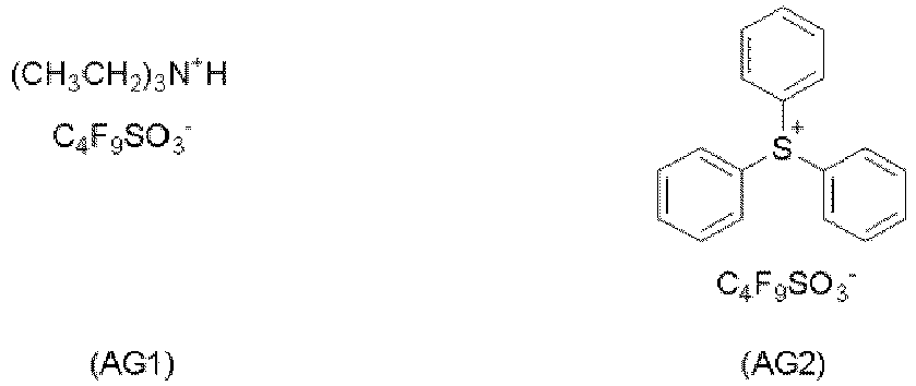
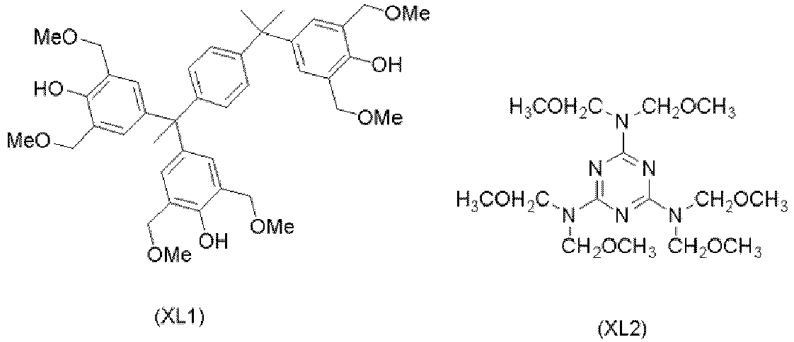
[Table 3] Composition for forming metal-containing film (A) Compound for forming metal-containing film Thermal acid generator Photo-acid generator Crosslinking agent High-boiling-point solvent Solvent (parts by mass) (parts by mass) (parts by mass) (parts by mass) (parts by mass) (parts by mass) MUL-1 A-1 (5) - - - PGMEA/PGME(65/30) MUL-2 A-2 (5) - - - PGMEA/PGME(65/30) MUL-3 A-3 (5) - - - PGMEA/PGME(65/30) MUL-4 A-4 (3) - - - PGMEA/PGME(67/30) MUL-5 A-5 (3) - - - PGMEA/PGME(67/30) MUL-6 A-6 (3) - - - PGMEA/PGME(67/30) MUL-7 A-7 (3) - - - PGMEA/PGME(67/30) MUL-8 A-8 (3) - - - PGMEA/PGME(67/30) MUL-9 A-9 (3) - - - PGMEA/PGME(67/30) MUL-10 A-10 (3) - - - PGMEA/PGME(67/30) MUL-11 A-11 (3) - - PGMEA/PGME(67/30) MUL-12 A-3 (5) AG1 (0.2) AG2 (0.2) - - PGMEA/PGME(65/30) MUL-13 A-3 (5) - - PGMEA/PGME(65/30) MUL-14 A-3 (5) - XL1 (0.5) - PGMEA/PGME(65/30) MUL-15 A-3 (5) AG1 (0.2) - XL2 (0.5) PGMEA/PGME(65/30) MUL-16 A-3 (5) - - F1 (5) PGMEA/PGME(65/30) Comparative MUL-1 R-1 (3) - - - - PGMEA/PGME(67/30) Comparative MUL-2 R-2 (3) - - - - PGMEA/PGME(67/30) - Each of the compositions (MUL-1 to -16 and comparative MUL-1 and -2) for forming a metal-containing film prepared above was respectively applied onto a silicon substrate, baked at the temperature shown in Table 4 for 60 seconds, then the thickness of the film from the center of the substrate to the periphery was measured, and the average film thickness (a [nm]) was calculated. Subsequently, a PGMEA solvent was dispensed thereon, left to stand for 30 seconds, then spin-drying was performed, then the PGMEA was evaporated by baking at 100°C for 60 seconds, and the film thickness (b [nm]) was measured. The difference between the film thicknesses of before and after the PGMEA treatment (film remaining percentage: (b/a) × 100) was calculated.
- In addition, regarding each of the cured films, a contact angle (CA1) with pure water was measured.
- The results are shown in Table 4 below.
[Table 4] Example Composition for forming metal-containing film Baking temperature Film thickness after film formation: a Film thickness after solvent treatment: b b/a × 100 Contact angle (CA1) Å Å % deg. Example 1-1 MUL-1 350°C 450.4 450.3 100% 68 Example 1-2 MUL-2 350°C 466.9 466.7 100% 65 Example 1-3 MUL-3 350°C 471.4 470.3 100% 70 Example 1-4 MUL-4 250°C 482.4 482.3 100% 62 Example 1-5 MUL-5 250°C 476.4 476.4 100% 63 Example 1-6 MUL-6 250°C 469.3 469.2 100% 63 Example 1-7 MUL-7 250°C 463.5 463.4 100% 68 Example 1-8 MUL-8 250°C 458.7 458.8 100% 63 Example 1-9 MUL-9 350°C 486.3 486.4 100% 72 Example 1-10 MUL-10 250°C 482.3 482.2 100% 73 Example 1-11 MUL-11 250°C 477.6 477.5 100% 66 Example 1-12 MUL-12 350°C 470.2 470.2 100% 74 Example 1-13 MUL-13 350°C 468.5 468.5 100% 71 Example 1-14 MUL-14 350°C 447.9 447.8 100% 71 Example 1-15 MUL-15 350°C 453.2 453.1 100% 76 Example 1-16 MUL-16 350°C 432.6 432.5 100% 70 Comparative Example 1-1 Comparative MUL-1 250°C 468.2 468.1 100% 35 Comparative Example 1-2 Comparative MUL-2 250°C 460.3 460.3 100% 50 - As shown in Table 4, it can be observed that in Examples 1-1 to 1-16, using the inventive compositions (MUL-1 to -16) for forming a metal-containing film, the compositions all had excellent film-formability and underwent hardly any film loss due to the solvent treatment, and achieved films having excellent solvent resistance. In addition, the films had a contact angle of over 60° to pure water by containing one of the groups represented by the formulae (a-1) to (a-3), and it can be seen that excellent adhesiveness to a resist pattern can be expected. It was also found that the contact angle was particularly high in Examples 1-12 and 1-15, where a composition containing the thermal acid generator (AG1) was used. It is conjectured that this is because curing caused by the ring-opening reaction of the epoxy or oxetane structure was promoted by the action of the acid generator, although the effect is uncertain.
- On the other hand, in Comparative Examples 1-1 and 1-2, using the compositions (comparative MUL-1 and -2), which are not the inventive composition for forming a metal-containing film, a film having excellent solvent resistance was obtained, but the contact angle to pure water was less than 60°.
- Each of the compositions (MUL-3 to -16 and comparative MUL-1 and -2) for forming a metal-containing film was respectively applied onto a silicon substrate, baked at the temperature shown in Table 5 for 60 seconds, and then the optical constants (refractive index "n" and attenuation coefficient "k") at a wavelength of 193 nm were determined by using a spectroscopic ellipsometer (VASE) with variable angle of incidence manufactured by J. A. Woollam Japan. The results are shown together in Table 5.
[Table 5] Example Composition for forming metal-containing film Baking temperature n k 193 nm 193 nm Example 2-1 MUL-3 350°C 1.91 0.19 Example 2-2 MUL-4 250°C 1.90 0.20 Example 2-3 MUL-5 250°C 1.88 0.21 Example 2-4 MUL-6 250°C 1.87 0.22 Example 2-5 MUL-7 250°C 1.89 0.22 Example 2-6 MUL-8 250°C 1.90 0.21 Example 2-7 MUL-9 350°C 1.92 0.22 Example 2-8 MUL-10 250°C 1.91 0.23 Example 2-9 MUL-11 250°C 1.90 0.23 Example 2-10 MUL-12 350°C 1.91 0.19 Example 2-11 MUL-13 350°C 1.91 0.19 Example 2-12 MUL-14 350°C 1.88 0.21 Example 2-13 MUL-15 350°C 1.91 0.23 Example 2-14 MUL-16 350°C 1.91 0.19 Comparative Example 2-1 Comparative MUL-1 250°C 2.10 0.30 Comparative Example 2-2 Comparative MUL-2 250°C 2.05 0.33 - As shown in Table 5, in Examples 2-1 to 2-14, where the inventive compositions (MUL-3 to -16) for forming a metal-containing film were used, the "n" value was 1.8 to 2.3 and the "k" value was 0.1 to 0.5 in every case.
- The optical constants also depend on the film thickness, the type of the resist upper layer film, etc., but as long as the "n" value is approximately between 1.8 and 2.3 and the "k" value is approximately between 0.1 and 0.5, light reflected from the substrate in ArF immersion and high-NA exposure can be considerably suppressed even when the metal-containing film is formed as a thin film of 20 nm or less, and the metal-containing film is applicable as a resist underlayer film for photoresist patterning. In the above-described Examples, the optical constants are in suitable ranges in every case, and it can be seen that the films are applicable as resist underlayer films in photoresist patterning.
- Each of the compositions (MUL-1 to -16 and comparative MUL-1 and -2) for forming a metal-containing film was respectively applied onto a silicon substrate and heated by using a hot plate at the same temperature as that shown in Table 4 for 60 seconds to form a metal-containing film having a film thickness of 50 nm (film thickness "a").
- In Comparative Example 3-3, the following silicon-containing resist middle layer film composition (SOG-1) was applied and baked at 220°C for 60 seconds to form a resist middle layer film having a film thickness of 50 nm (film thickness "a").
- The silicon-containing resist middle layer film composition (SOG-1) was prepared by dissolving an ArF silicon-containing resist middle layer film polymer represented by (SiP1) and a thermal crosslinking catalyst (CAT1) in a solvent containing 0.1 mass% of FC-4430 (available from Sumitomo 3M Limited) in the proportion shown in Table 6; and filtering the solution through a filter made of a fluororesin and having a pore size of 0.1 µm.
[Table 6] Polymer Thermal crosslinking catalyst Solvent 1 Solvent 2 (parts by mass) (parts by mass) (parts by mass) (parts by mass) SOG-1 SiP1 CAT1 Propylene glycol monoethyl ether Pure water (100) (1) (2,900) (400) - The structural formulae of the used ArF silicon-containing resist middle layer film polymer (SiP1) and thermal crosslinking catalyst (CAT1) are shown below.

- In Comparative Example 3-4, the following organic resist underlayer film composition (SOC-1) was applied and baked at 350°C for 60 seconds to form a resist underlayer film having a film thickness of 50 nm (film thickness "a").
- The organic resist underlayer film composition (SOC-1) was prepared by dissolving an organic resist underlayer film polymer represented by (CP1) in a solvent containing 0.1 mass% of FC-4430 (available from Sumitomo 3M Limited) in the proportion shown in Table 7; and filtering the solution through a filter made of a fluororesin and having a pore size of 0.1 µm.
[Table 7] Polymer Solvent 1 (parts by mass) (parts by mass) SOC-1 CP1 Propylene glycol monoethyl ether (100) (3,000) - The structural formula of the used organic resist underlayer film polymer (CP1) is shown below.

- Subsequently, using an etching apparatus CE-300I manufactured by ULVAC, Inc., etching using a CF4 gas and O2 gas was each performed under the following conditions, and the film thickness "b" was measured. Then, the film thickness etched in one minute was calculated as an etching rate (nm/min) from the film thickness etched (film thickness "a" - film thickness "b") using the respective gas in a specified time, and etching resistance was evaluated.
- When the etching rate to CF4 gas was lower than 20 nm/min, the evaluation "A (very good)" was given, when 20 nm/min to 30 nm/min, "B (good)", and when over 30 nm/min, "C (poor)".
- When the etching rate to O2 gas was lower than 20 nm/min, the evaluation "A (very good)" was given, when 20 nm/min to 30 nm/min, "B (good)", and when over 30 nm/min, "C (poor)".
- Table 8 shows the results.
-
- Pressure: 3 Pa
- Antenna RF power: 100 W
- Bias RF power: 15 W
- CF4 gas flow rate: 15 sccm
- Time: 30 sec
-
- Pressure: 3 Pa
- Antenna RF power: 300 W
- Bias RF power: 10 W
- O2 gas flow rate: 25 sccm
- Time: 30 sec
- As shown in Table 8, it was shown that in Examples 3-1 to 3-16, where the inventive compositions (MUL-1 to -16) for forming a metal-containing film were used, the compositions all exhibited excellent etching resistance to CF4 gas and O2 gas.
- The inventive compositions for forming a metal-containing film have better resistance than SOG-1, used in Comparative Example 3-3, to etching using CF4 gas, and therefore, it can be said that the compositions are suitable for a three-layer resist process, where a resist pattern is transferred to a substrate to be processed by employing a combination with a resist underlayer film.
- In addition, since the inventive compositions have better etching resistance to O2 gas compared with SOC-1, used in Comparative Example 3-4, it can be said that the compositions are suitable for a two-layer resist process, where a resist pattern is transferred to a substrate to be processed by employing a combination with a photoresist upper layer film.
- Using the above-described SOC-1, an SiO2 wafer was spin-coated, and the coating film was baked at 350°C for 60 seconds to fabricate a carbon film having a thickness of 60 nm as a resist underlayer film on the substrate. The carbon film had a carbon content of 46 atomic% and the optical constants (n/k) at a wavelength of 193 nm were 1.42/0.50. A composition obtained by diluting one of the compositions (MUL-3 to -16 and comparative MUL-1 and -2) for forming a metal-containing film with an organic solvent (PGMEA/PGME = 700/300 parts by mass) was applied thereto, and heated by using a hot plate at the same temperature as that shown in Table 4 for 60 seconds to form a metal-containing film having a thickness of 15 nm. A monolayer resist for ArF as a resist upper layer film composition was applied thereto and baked at 105°C for 60 seconds to form a photoresist film having a thickness of 100 nm. A liquid immersion top coat composition (TC-1) was applied to the photoresist film and baked at 90°C for 60 seconds to form a top coat having a thickness of 50 nm.
- The resist upper layer film material (monolayer resist for ArF) was prepared by dissolving a polymer (RP1), an acid generator (PAG1), and a basic compound (Amine1), each in the proportion shown in Table 9, in a solvent containing 0.1% by mass of a surfactant FC-4430 (available from Sumitomo 3M Limited), and filtering the solution through a 0.1-pm filter made of a fluororesin.
[Table 9] Polymer (parts by mass) Acid generator (parts by mass) Basic compound (parts by mass) Solvent (parts by mass) Monolayer resist for ArF RP1 (100) PAG1 (6.6) Amine1 (0.8) PGMEA (2,500) - The polymer (RP1), the acid generator (PAG1), and the basic compound (Amine1) used for the resist upper layer film material (monolayer resist for ArF) are shown below.


- The liquid immersion top coat composition (TC-1) was prepared by dissolving a top coat polymer (PP1) in an organic solvent at the proportion shown in Table 10, and filtering the solution through a 0.1-pm filter made of a fluororesin.
[Table 10] Top coat polymer (parts by mass) Organic solvent (parts by mass) TC-1 PP1 (100) Diisoamyl ether (2,700) 2-methyl-1-butanol (270) - The top coat polymer (PP1) used for the liquid immersion top coat composition (TC-1) is shown below.

- Then, the substrate was exposed to light with an ArF liquid immersion exposure apparatus (NSR-S610C manufactured by Nikon Corporation, NA: 1.30, σ: 0.98/0.78, 35° s-polarized dipole illumination, 6% halftone phase shift mask), baked at 100°C for 60 seconds (PEB), and developed with a 2.38% by mass aqueous solution of tetramethylammonium hydroxide (TMAH) for 30 seconds, thereby obtaining a 50 nm 1:1 positive line-and-space pattern (a resist upper layer film pattern).
- The calculation of reflectance was carried out using PROLITH 2020a (manufactured by Litho Tech Japan Corporation). With the film thickness of the metal-containing film fixed to 10 nm, the reflectance at which the "n" of the metal-containing film is 1.60 to 2.20 and the "k" is 0.15 to 0.50 was calculated, and the results are shown in
FIG. 3 . The optical constants (n/k) at which it is possible to reduce the reflected light from the underlying substrate during pattern exposure to 1.0% or less are preferable. - The pattern cross section was observed with S-4700 (electron microscope manufactured by Hitachi, Ltd.).
- Table 11 shows the results.
- Subsequently, the metal-containing film was etched by dry etching while using the resist upper layer film pattern as a mask to form a metal-containing film pattern, the resist underlayer film was etched while using the obtained metal-containing film pattern as a mask to form a resist underlayer film pattern, and the SiO2 film was etched while using the obtained resist underlayer film pattern as a mask. The etching conditions were as follows.
- The pattern cross section was observed with S-4700 (electron microscope manufactured by Hitachi, Ltd.).
- Table 11 shows the results.
-
- Pressure: 1 Pa
- Antenna RF power: 320 W
- Bias RF power: 30 W
- Cl2 gas flow rate: 25 sccm
- Time: 15 sec
-
- Pressure: 1 Pa
- Antenna RF power: 300 W
- Bias RF power: 10 W
- O2 gas flow rate: 25 sccm
- Time: 20 sec
-
- Pressure: 1 Pa
- Antenna RF power: 100 W
- Bias RF power: 15 W
- CF4 gas flow rate: 15 sccm
- Time: 60 sec
- As shown in Table 11, in Examples 4-1 to 4-14, where the inventive compositions (MUL-3 to -16) for forming a metal-containing film were used, it was observed that the pattern profile after development was excellent in every case. It is conjectured that since the inventive compositions for forming a metal-containing film each contain a compound for forming a metal-containing film containing one of the groups represented by the formulae (a-1) to (a-3), the compositions have high adhesiveness to the resist pattern and also have optical constants that allow sufficient reduction in the light reflected from the substrate during pattern exposure, and that therefore, excellent resist patterns were obtained. In addition, after the etching after transference to the substrate, the resist upper layer film pattern was successfully transferred to the substrate in the end, and it was confirmed that the compositions can be used suitably in fine processing according to a multilayer resist method.
- On the other hand, in Comparative Examples 4-1 and 4-2, using comparative MUL-1 and -2, which had a low contact angle in the contact angle evaluation, collapse of the resist upper layer film pattern was observed after development.
- From the above, the inventive compound for forming a metal-containing film, the inventive composition containing the compound, and the inventive patterning processes using the composition provide high adhesiveness to a resist upper layer film pattern, have an effect of suppressing the collapse of a fine pattern, and give a high-rectangularity pattern profile of a resist upper layer film, and therefore, are particularly suitably used in multilayer resist processes and are extremely useful in fine patterning for manufacturing semiconductor devices.
- The present description includes the following embodiments.
- [1]: A compound for forming a metal-containing film, comprising: at least one metal atom selected from the group consisting of Ti, Zr, and Hf; and a ligand coordinated to the metal atom, wherein the ligand contains a group represented by any of the following formulae (a-1) to (a-3),

- [2]: The compound for forming a metal-containing film of the above [1], wherein the ligand is derived from a structure represented by the following general formula (1) or (2),
RaXOH (1)
RaXCOOH (2)
wherein Ra represents a group represented by any of the formulae (a-1) to (a-3); and X represents a divalent organic group having 1 to 20 carbon atoms. - [3]: The compound for forming a metal-containing film of the above [2], wherein the X is a hydrocarbon group having 1 to 10 carbon atoms, the structure represented by the general formula (2) is a structure represented by the following general formula (x-1) or (x-2), or the structure represented by the general formula (1) is a structure represented by the following formula (x-3),


- [4]: The compound for forming a metal-containing film of the above [3], wherein the Y1 to Y4 are each a divalent hydrocarbon group having 1 to 10 carbon atoms.
- [5]: The compound for forming a metal-containing film of any one of the above [2] to [4], wherein the compound for forming a metal-containing film is a reaction product of a reaction between: a metal compound represented by the following general formula (3) or a metal-containing compound containing a hydrolysate, condensate, or hydrolysis condensate of the metal compound represented by the following general formula (3); and the structure represented by the general formula (1) or (2),
LaMXb (3)
wherein M represents any of Ti, Zr, and Hf, L represents a monodentate ligand having 1 to 30 carbon atoms or a polydentate ligand having 1 to 30 carbon atoms, X represents a hydrolysable group selected from a halogen atom, an alkoxy group, a carboxylate group, an acyloxy group, and -NR1R2, R1 and R2 each independently represent a hydrogen atom or a monovalent organic group having 1 to 20 carbon atoms, and a+b = 4, "a" and "b" each representing an integer of 0 to 4. - [6]: The compound for forming a metal-containing film of the above [5], wherein the metal compound has a structure represented by the following general formula (4),
M(OR1A)4 (4)
wherein M is as defined above; and R1A represents a monovalent organic group having 1 to 20 carbon atoms. - [7] : The compound for forming a metal-containing film of any one of the above [1] to [6], further comprising a ligand derived from a silicon compound represented by the following general formula (5),


- [8]: A composition for forming a metal-containing film, comprising: (A) the compound for forming a metal-containing film of any one of the above [1] to [7]; and (B) an organic solvent.
- [9]: The composition for forming a metal-containing film of the above [8], further comprising one or more of (C) a thermal acid generator and (D) a photo-acid generator.
- [10]: The composition for forming a metal-containing film of the above [8] or [9], further comprising one or more of (E) a crosslinking agent and (G) a surfactant.
- [11]: The composition for forming a metal-containing film of any one of the above [8] to [10], wherein the organic solvent (B) is a mixture of one or more kinds of organic solvent having a boiling point of lower than 180°C and one or more kinds of organic solvent having a boiling point of 180°C or higher.
- [12]: A patterning process for forming a pattern in a substrate to be processed, comprising the steps of:
- (I-1) applying the composition for forming a metal-containing film of any one of the above [8] to [11] onto a substrate to be processed, followed by heating to form a metal-containing film;
- (I-2) forming a resist upper layer film on the metal-containing film by using a photoresist material;
- (I-3) subjecting the resist upper layer film to pattern exposure and then development with a developer to form a pattern in the resist upper layer film;
- (I-4) transferring the pattern to the metal-containing film by dry etching while using the resist upper layer film having the formed pattern as a mask; and
- (I-5) processing the substrate to be processed while using the metal-containing film having the transferred pattern as a mask to form the pattern in the substrate to be processed.
- [13]: A patterning process for forming a pattern in a substrate to be processed, comprising the steps of:
- (II-1) forming a resist underlayer film on a substrate to be processed;
- (II-2) applying the composition for forming a metal-containing film of any one of the above [8] to [11] onto the resist underlayer film, followed by heating to form a metal-containing film;
- (II-3) forming a resist upper layer film on the metal-containing film by using a photoresist material;
- (II-4) subjecting the resist upper layer film to pattern exposure and then development with a developer to form a pattern in the resist upper layer film;
- (II-5) transferring the pattern to the metal-containing film by dry etching while using the resist upper layer film having the formed pattern as a mask;
- (II-6) transferring the pattern to the resist underlayer film by dry etching while using the metal-containing film having the transferred pattern as a mask; and
- (II-7) processing the substrate to be processed while using the resist underlayer film having the transferred pattern as a mask to form the pattern in the substrate to be processed.
- [14]: A method for manufacturing a compound for forming a metal-containing film, the method comprising performing a reaction between: a metal compound containing at least one metal atom selected from the group consisting of Ti, Zr, and Hf; and a ligand containing a group represented by any of the following formulae (a-1) to (a-3),

- [15]: The method of the above [14] for manufacturing a compound for forming a metal-containing film, wherein the ligand has a structure represented by the following general formula (1) or (2),
RaXOH (1)
RaXCOOH (2)
wherein Ra represents a group represented by any of the formulae (a-1) to (a-3); and X represents a divalent organic group having 1 to 20 carbon atoms. - [16]: The method of the above [15] for manufacturing a compound for forming a metal-containing film, wherein, in the ligand, the X is a hydrocarbon group having 1 to 10 carbon atoms, the structure represented by the general formula (2) is a structure represented by the following general formula (x-1) or (x-2), or the structure represented by the general formula (1) is a structure represented by the following formula (x-3),
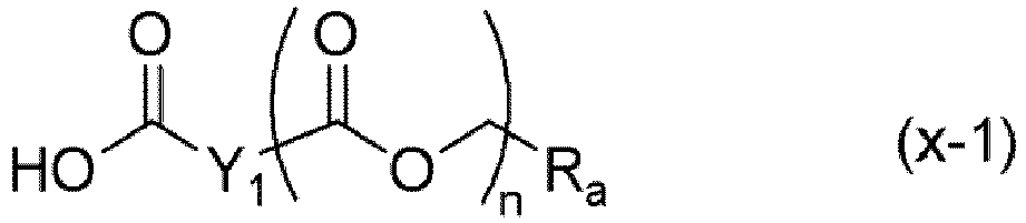


- [17] : The method of the above [16] for manufacturing a compound for forming a metal-containing film, wherein the Y1 to Y4 are each a divalent hydrocarbon group having 1 to 10 carbon atoms.
- [18]: The method of any one of the above [15] to [17] for manufacturing a compound for forming a metal-containing film, wherein the compound for forming a metal-containing film is a reaction product of a reaction between: a metal compound represented by the following general formula (3) or a metal-containing compound containing a hydrolysate, condensate, or hydrolysis condensate of the metal compound represented by the following general formula (3); and the structure represented by the general formula (1) or (2),
LaMXb (3)
wherein M represents any of Ti, Zr, and Hf, L represents a monodentate ligand having 1 to 30 carbon atoms or a polydentate ligand having 1 to 30 carbon atoms, X represents a hydrolysable group selected from a halogen atom, an alkoxy group, a carboxylate group, an acyloxy group, and -NR1R2, R1 and R2 each independently represent a hydrogen atom or a monovalent organic group having 1 to 20 carbon atoms, and a+b = 4, "a" and "b" each representing an integer of 0 to 4. - [19]: The method of the above [18] for manufacturing a compound for forming a metal-containing film, wherein the metal compound has a structure represented by the following general formula (4),
M(OR1A)4 (4)
wherein M is as defined above; and R1A represents a monovalent organic group having 1 to 20 carbon atoms. - It should be noted that the present invention is not limited to the above-described embodiments. The embodiments are just examples, and any examples that have substantially the same feature and demonstrate the same functions and effects as those in the technical concept disclosed in claims of the present invention are included in the technical scope of the present invention. The present invention also refers to the following numbered embodiments, wherein the term "claim" means "embodiment":
- 1. A compound for forming a metal-containing film, comprising: at least one metal atom selected from the group consisting of Ti, Zr, and Hf; and a ligand coordinated to the metal atom, wherein the ligand contains a group represented by any of the following formulae (a-1) to (a-3),

- 2. The compound for forming a metal-containing film according to
claim 1, wherein the ligand is derived from a structure represented by the following general formula (1) or (2),
RaXOH (1)
RaXCOOH (2)
wherein Ra represents a group represented by any of the formulae (a-1) to (a-3); and X represents a divalent organic group having 1 to 20 carbon atoms. - 3. The compound for forming a metal-containing film according to
claim 2, wherein the X is a hydrocarbon group having 1 to 10 carbon atoms, the structure represented by the general formula (2) is a structure represented by the following general formula (x-1) or (x-2), or the structure represented by the general formula (1) is a structure represented by the following formula (x-3),


- 4. The compound for forming a metal-containing film according to
claim 3, wherein the Y1 to Y4 are each a divalent hydrocarbon group having 1 to 10 carbon atoms. - 5. The compound for forming a metal-containing film according to any one of
claims 2 to 4, wherein the compound for forming a metal-containing film is a reaction product of a reaction between: a metal compound represented by the following general formula (3) or a metal-containing compound containing a hydrolysate, condensate, or hydrolysis condensate of the metal compound represented by the following general formula (3); and the structure represented by the general formula (1) or (2),
LaMXb (3)
wherein M represents any of Ti, Zr, and Hf, L represents a monodentate ligand having 1 to 30 carbon atoms or a polydentate ligand having 1 to 30 carbon atoms, X represents a hydrolysable group selected from a halogen atom, an alkoxy group, a carboxylate group, an acyloxy group, and -NR1R2, R1 and R2 each independently represent a hydrogen atom or a monovalent organic group having 1 to 20 carbon atoms, and a+b = 4, "a" and "b" each representing an integer of 0 to 4. - 6. The compound for forming a metal-containing film according to claim 5, wherein the metal compound has a structure represented by the following general formula (4),
M(OR1A)4 (4)
wherein M is as defined above; and R1A represents a monovalent organic group having 1 to 20 carbon atoms. - 7. The compound for forming a metal-containing film according to any one of
claims 1 to 6, further comprising a ligand derived from a silicon compound represented by the following general formula (5),

- 8. A composition for forming a metal-containing film, comprising: (A) the compound for forming a metal-containing film according to any one of
claims 1 to 7; and (B) an organic solvent. - 9. The composition for forming a metal-containing film according to claim 8, further comprising one or more of (C) a thermal acid generator and (D) a photo-acid generator.
- 10. The composition for forming a metal-containing film according to claim 8 or 9, further comprising one or more of (E) a crosslinking agent and (G) a surfactant.
- 11. The composition for forming a metal-containing film according to any one of claims 8 to 10, wherein the organic solvent (B) is a mixture of one or more kinds of organic solvent having a boiling point of lower than 180°C and one or more kinds of organic solvent having a boiling point of 180°C or higher.
- 12. A patterning process for forming a pattern in a substrate to be processed, comprising the steps of:
- (I-1) applying the composition for forming a metal-containing film according to any one of claims 8 to 11 onto a substrate to be processed, followed by heating to form a metal-containing film;
- (I-2) forming a resist upper layer film on the metal-containing film by using a photoresist material;
- (I-3) subjecting the resist upper layer film to pattern exposure and then development with a developer to form a pattern in the resist upper layer film;
- (I-4) transferring the pattern to the metal-containing film by dry etching while using the resist upper layer film having the formed pattern as a mask; and
- (I-5) processing the substrate to be processed while using the metal-containing film having the transferred pattern as a mask to form the pattern in the substrate to be processed.
- 13. A patterning process for forming a pattern in a substrate to be processed, comprising the steps of:
- (II-1) forming a resist underlayer film on a substrate to be processed;
- (II-2) applying the composition for forming a metal-containing film according to any one of claims 8 to 11 onto the resist underlayer film, followed by heating to form a metal-containing film;
- (II-3) forming a resist upper layer film on the metal-containing film by using a photoresist material;
- (II-4) subjecting the resist upper layer film to pattern exposure and then development with a developer to form a pattern in the resist upper layer film;
- (II-5) transferring the pattern to the metal-containing film by dry etching while using the resist upper layer film having the formed pattern as a mask;
- (II-6) transferring the pattern to the resist underlayer film by dry etching while using the metal-containing film having the transferred pattern as a mask; and
- (II-7) processing the substrate to be processed while using the resist underlayer film having the transferred pattern as a mask to form the pattern in the substrate to be processed.
- 14. A method for manufacturing a compound for forming a metal-containing film, the method comprising performing a reaction between: a metal compound containing at least one metal atom selected from the group consisting of Ti, Zr, and Hf; and a ligand containing a group represented by any of the following formulae (a-1) to (a-3),

- 15. The method according to claim 14 for manufacturing a compound for forming a metal-containing film, wherein the ligand has a structure represented by the following general formula (1) or (2),
RaXOH (1)
RaXCOOH (2)
wherein Ra represents a group represented by any of the formulae (a-1) to (a-3); and X represents a divalent organic group having 1 to 20 carbon atoms. - 16. The method according to claim 15 for manufacturing a compound for forming a metal-containing film, wherein, in the ligand, the X is a hydrocarbon group having 1 to 10 carbon atoms, the structure represented by the general formula (2) is a structure represented by the following general formula (x-1) or (x-2), or the structure represented by the general formula (1) is a structure represented by the following formula (x-3),


- 17. The method according to claim 16 for manufacturing a compound for forming a metal-containing film, wherein the Y1 to Y4 are each a divalent hydrocarbon group having 1 to 10 carbon atoms.
- 18. The method according to any one of
claims 15 to 17 for manufacturing a compound for forming a metal-containing film, wherein the compound for forming a metal-containing film is a reaction product of a reaction between: a metal compound represented by the following general formula (3) or a metal-containing compound containing a hydrolysate, condensate, or hydrolysis condensate of the metal compound represented by the following general formula (3); and the structure represented by the general formula (1) or (2),
LaMXb (3)
wherein M represents any of Ti, Zr, and Hf, L represents a monodentate ligand having 1 to 30 carbon atoms or a polydentate ligand having 1 to 30 carbon atoms, X represents a hydrolysable group selected from a halogen atom, an alkoxy group, a carboxylate group, an acyloxy group, and -NR1R2, R1 and R2 each independently represent a hydrogen atom or a monovalent organic group having 1 to 20 carbon atoms, and a+b = 4, "a" and "b" each representing an integer of 0 to 4. - 19. The method according to claim 18 for manufacturing a compound for forming a metal-containing film, wherein the metal compound has a structure represented by the following general formula (4),
M(OR1A)4 (4)
wherein M is as defined above; and R1A represents a monovalent organic group having 1 to 20 carbon atoms.
| Example | Composition for forming metal-containing film | Etching rate (nm/min) | Etching rate (nm/min) |
| CF4 | O2 | ||
| Example 3-1 | MUL-1 | A | A |
| Example 3-2 | MUL-2 | A | A |
| Example 3-3 | MUL-3 | A | A |
| Example 3-4 | MUL-4 | A | A |
| Example 3-5 | MUL-5 | A | A |
| Example 3-6 | MUL-6 | A | A |
| Example 3-7 | MUL-7 | A | A |
| Example 3-8 | MUL-8 | A | A |
| Example 3-9 | MUL-9 | A | A |
| Example 3-10 | MUL-10 | A | A |
| Example 3-11 | MUL-11 | A | A |
| Example 3-12 | MUL-12 | A | A |
| Example 3-13 | MUL-13 | A | A |
| Example 3-14 | MUL-14 | A | A |
| Example 3-15 | MUL-15 | A | A |
| Example 3-16 | MUL-16 | A | A |
| Comparative Example 3-1 | Comparative MUL-1 | A | A |
| Comparative Example 3-2 | Comparative MUL-2 | A | A |
| Comparative Example 3-3 | SOG-1 | C | B |
| Comparative Example 3-4 | SOC-1 | B | C |
| Example | Composition for forming metal-containing film | Reflectance | After development | After etching for transfer to substrate |
| % | Pattern profile | Pattern profile | ||
| Example 4-1 | MUL-3 | 0.6% | Vertical profile | Vertical profile |
| Example 4-2 | MUL-4 | 0.6% | Vertical profile | Vertical profile |
| Example 4-3 | MUL-5 | 0.5% | Vertical profile | Vertical profile |
| Example 4-4 | MUL-6 | 0.5% | Vertical profile | Vertical profile |
| Example 4-5 | MUL-7 | 0.4% | Vertical profile | Vertical profile |
| Example 4-6 | MUL-8 | 0.5% | Vertical profile | Vertical profile |
| Example 4-7 | MUL-9 | 0.4% | Vertical profile | Vertical profile |
| Example 4-8 | MUL-10 | 0.3% | Vertical profile | Vertical profile |
| Example 4-9 | MUL-11 | 0.3% | Vertical profile | Vertical profile |
| Example 4-10 | MUL-12 | 0.7% | Vertical profile | Vertical profile |
| Example 4-11 | MUL-13 | 0.7% | Vertical profile | Vertical profile |
| Example 4-12 | MUL-14 | 0.5% | Vertical profile | Vertical profile |
| Example 4-13 | MUL-15 | 0.3% | Vertical profile | Vertical profile |
| Example 4-14 | MUL-16 | 0.7% | Vertical profile | Vertical profile |
| Comparative Example 4-1 | Comparative MUL-1 | 1.4% | Pattern collapse | - |
| Comparative Example 4-2 | Comparative MUL-2 | 0.7% | Pattern collapse | - |
Claims (15)
- A compound for forming a metal-containing film, comprising: at least one metal atom selected from the group consisting of Ti, Zr, and Hf; and a ligand coordinated to the metal atom, wherein the ligand contains a group represented by any of the following formulae (a-1) to (a-3),

- The compound for forming a metal-containing film according to claim 1, wherein the ligand is derived from a structure represented by the following general formula (1) or (2),
RaXOH (1)
RaXCOOH (2)
wherein Ra represents a group represented by any of the formulae (a-1) to (a-3); and X represents a divalent organic group having 1 to 20 carbon atoms. - The compound for forming a metal-containing film according to claim 2, wherein the X is a hydrocarbon group having 1 to 10 carbon atoms, the structure represented by the general formula (2) is a structure represented by the following general formula (x-1) or (x-2), or the structure represented by the general formula (1) is a structure represented by the following formula (x-3),


- The compound for forming a metal-containing film according to claim 3, wherein the Y1 to Y4 are each a divalent hydrocarbon group having 1 to 10 carbon atoms.
- The compound for forming a metal-containing film according to any one of claims 2 to 4, wherein the compound for forming a metal-containing film is a reaction product of a reaction between: a metal compound represented by the following general formula (3) or a metal-containing compound containing a hydrolysate, condensate, or hydrolysis condensate of the metal compound represented by the following general formula (3); and the structure represented by the general formula (1) or (2),
LaMXb (3)
wherein M represents any of Ti, Zr, and Hf, L represents a monodentate ligand having 1 to 30 carbon atoms or a polydentate ligand having 1 to 30 carbon atoms, X represents a hydrolysable group selected from a halogen atom, an alkoxy group, a carboxylate group, an acyloxy group, and -NR1R2, R1 and R2 each independently represent a hydrogen atom or a monovalent organic group having 1 to 20 carbon atoms, and a+b = 4, "a" and "b" each representing an integer of 0 to 4;preferably
wherein the metal compound has a structure represented by the following general formula (4),
M(OR1A)4 (4)
wherein M is as defined above; and R1A represents a monovalent organic group having 1 to 20 carbon atoms. - The compound for forming a metal-containing film according to any one of claims 1 to 5, further comprising a ligand derived from a silicon compound represented by the following general formula (5),
 wherein R3A, R3B, and R3C each represent any organic group selected from an organic group having 2 to 30 carbon atoms including a crosslinking group of a structure represented by any of the following general formulae (b-1) to (b-3), a substituted or unsubstituted alkyl group having 1 to 20 carbon atoms, and an aryl group having 6 to 20 carbon atoms,
 wherein R3 represents a hydrogen atom or a monovalent organic group having 1 to 10 carbon atoms; "q" represents 0 or 1; and "*" represents an attachment point.
 - A composition for forming a metal-containing film, comprising: (A) the compound for forming a metal-containing film according to any one of claims 1 to 6; and (B) an organic solvent.
- The composition for forming a metal-containing film according to claim 7, further comprising one or more of (C) a thermal acid generator and (D) a photo-acid generator.
- The composition for forming a metal-containing film according to claim 7 or 8, further comprising one or more of (E) a crosslinking agent and (G) a surfactant.
- The composition for forming a metal-containing film according to any one of claims 7 to 9, wherein the organic solvent (B) is a mixture of one or more kinds of organic solvent having a boiling point of lower than 180°C and one or more kinds of organic solvent having a boiling point of 180°C or higher.
- A patterning process for forming a pattern in a substrate to be processed, comprising the steps of:A)(I-1) applying the composition for forming a metal-containing film according to any one of claims 7 to 10 onto a substrate to be processed, followed by heating to form a metal-containing film;(I-2) forming a resist upper layer film on the metal-containing film by using a photoresist material;(I-3) subjecting the resist upper layer film to pattern exposure and then development with a developer to form a pattern in the resist upper layer film;(I-4) transferring the pattern to the metal-containing film by dry etching while using the resist upper layer film having the formed pattern as a mask; and(I-5) processing the substrate to be processed while using the metal-containing film having the transferred pattern as a mask to form the pattern in the substrate to be processed;orB)(II-1) forming a resist underlayer film on a substrate to be processed;(II-2) applying the composition for forming a metal-containing film according to any one of claims 7 to 10 onto the resist underlayer film, followed by heating to form a metal-containing film;(II-3) forming a resist upper layer film on the metal-containing film by using a photoresist material;(II-4) subjecting the resist upper layer film to pattern exposure and then development with a developer to form a pattern in the resist upper layer film;(II-5) transferring the pattern to the metal-containing film by dry etching while using the resist upper layer film having the formed pattern as a mask;(II-6) transferring the pattern to the resist underlayer film by dry etching while using the metal-containing film having the transferred pattern as a mask; and(II-7) processing the substrate to be processed while using the resist underlayer film having the transferred pattern as a mask to form the pattern in the substrate to be processed.
- A method for manufacturing a compound for forming a metal-containing film, the method comprising performing a reaction between: a metal compound containing at least one metal atom selected from the group consisting of Ti, Zr, and Hf; and a ligand containing a group represented by any of the following formulae (a-1) to (a-3),

- The method according to claim 12 for manufacturing a compound for forming a metal-containing film, wherein the ligand has a structure represented by the following general formula (1) or (2),
RaXOH (1)
RaXCOOH (2)
wherein Ra represents a group represented by any of the formulae (a-1) to (a-3); and X represents a divalent organic group having 1 to 20 carbon atoms. - The method according to claim 13 for manufacturing a compound for forming a metal-containing film, wherein, in the ligand, the X is a hydrocarbon group having 1 to 10 carbon atoms, the structure represented by the general formula (2) is a structure represented by the following general formula (x-1) or (x-2), or the structure represented by the general formula (1) is a structure represented by the following formula (x-3),

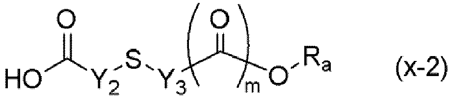
 wherein Y4 represents a divalent organic group having 1 to 10 carbon atoms; Ra is as defined above; and "l" represents 0 or 1;preferably
wherein the Y1 to Y4 are each a divalent hydrocarbon group having 1 to 10 carbon atoms. - The method according to claim 13 or 14 for manufacturing a compound for forming a metal-containing film, wherein the compound for forming a metal-containing film is a reaction product of a reaction between: a metal compound represented by the following general formula (3) or a metal-containing compound containing a hydrolysate, condensate, or hydrolysis condensate of the metal compound represented by the following general formula (3); and the structure represented by the general formula (1) or (2),
LaMXb (3)
wherein M represents any of Ti, Zr, and Hf, L represents a monodentate ligand having 1 to 30 carbon atoms or a polydentate ligand having 1 to 30 carbon atoms, X represents a hydrolysable group selected from a halogen atom, an alkoxy group, a carboxylate group, an acyloxy group, and -NR1R2, R1 and R2 each independently represent a hydrogen atom or a monovalent organic group having 1 to 20 carbon atoms, and a+b = 4, "a" and "b" each representing an integer of 0 to 4;preferablywherein the metal compound has a structure represented by the following general formula (4),
M(OR1A)4 (4)
wherein M is as defined above; and R1A represents a monovalent organic group having 1 to 20 carbon atoms.
Applications Claiming Priority (1)
| Application Number | Priority Date | Filing Date | Title |
|---|---|---|---|
| JP2023113111 | 2023-07-10 |
Publications (1)
| Publication Number | Publication Date |
|---|---|
| EP4495688A1 true EP4495688A1 (en) | 2025-01-22 |
Family
ID=91616506
Family Applications (1)
| Application Number | Title | Priority Date | Filing Date |
|---|---|---|---|
| EP24183158.5A Pending EP4495688A1 (en) | 2023-07-10 | 2024-06-19 | Compound for forming metal-containing film, composition for forming metal-containing film, patterning process, and method for manufacturing compound for forming metal-containing film |
Country Status (7)
| Country | Link |
|---|---|
| US (1) | US20250036024A1 (en) |
| EP (1) | EP4495688A1 (en) |
| JP (1) | JP2025011028A (en) |
| KR (1) | KR102939481B1 (en) |
| CN (1) | CN119285667A (en) |
| IL (1) | IL313603A (en) |
| TW (1) | TWI898715B (en) |
Citations (37)
| Publication number | Priority date | Publication date | Assignee | Title |
|---|---|---|---|---|
| JP2004205685A (en) | 2002-12-24 | 2004-07-22 | Shin Etsu Chem Co Ltd | Pattern forming method and underlayer film forming material |
| JP2004264710A (en) | 2003-03-04 | 2004-09-24 | Jsr Corp | Antireflection film forming composition and antireflection film |
| JP2005043471A (en) | 2003-07-23 | 2005-02-17 | Jsr Corp | Antireflection film forming composition and method for forming antireflection film |
| JP2005070318A (en) * | 2003-08-22 | 2005-03-17 | Fuji Photo Film Co Ltd | Antidazzle and antireflection film and method for manufacturing the same, polarizing plate and image display device |
| JP2005128509A (en) | 2003-10-03 | 2005-05-19 | Shin Etsu Chem Co Ltd | Photoresist underlayer film forming material and pattern forming method |
| JP2005520354A (en) | 2002-07-11 | 2005-07-07 | インターナショナル・ビジネス・マシーンズ・コーポレーション | Silicon-containing antireflection composition as a hard mask layer |
| JP2005250434A (en) | 2004-02-04 | 2005-09-15 | Shin Etsu Chem Co Ltd | Resist underlayer film material and pattern forming method |
| JP2006259482A (en) | 2005-03-18 | 2006-09-28 | Shin Etsu Chem Co Ltd | Photoresist underlayer film forming material and pattern forming method |
| JP2006259249A (en) | 2005-03-17 | 2006-09-28 | Shin Etsu Chem Co Ltd | Photoresist underlayer film forming material and pattern forming method |
| JP2006293298A (en) | 2005-03-11 | 2006-10-26 | Shin Etsu Chem Co Ltd | Photoresist underlayer film forming material and pattern forming method |
| JP2007171895A (en) | 2005-11-28 | 2007-07-05 | Shin Etsu Chem Co Ltd | Resist underlayer film material and pattern forming method |
| JP2007199653A (en) | 2005-12-27 | 2007-08-09 | Shin Etsu Chem Co Ltd | Photoresist underlayer film forming material and pattern forming method |
| JP2007293294A (en) | 2006-03-27 | 2007-11-08 | Jsr Corp | Fine pattern forming method and polymer |
| JP2007316282A (en) | 2006-05-25 | 2007-12-06 | Shin Etsu Chem Co Ltd | Photoresist underlayer film forming material and pattern forming method |
| JP2008065303A (en) | 2006-08-10 | 2008-03-21 | Shin Etsu Chem Co Ltd | Resist underlayer film material and pattern forming method |
| JP2008274250A (en) | 2007-04-06 | 2008-11-13 | Osaka Gas Co Ltd | Phenolic resin and method for producing the same |
| JP2009014816A (en) | 2007-07-02 | 2009-01-22 | Jsr Corp | Resist underlayer film forming composition and pattern forming method |
| JP2009126940A (en) | 2007-11-22 | 2009-06-11 | Shin Etsu Chem Co Ltd | Metal oxide-containing film forming composition, metal oxide-containing film, metal oxide-containing film forming substrate, and pattern forming method using the same |
| JP2009269953A (en) | 2008-05-01 | 2009-11-19 | Shin Etsu Chem Co Ltd | New photoacid generator, resist material using the same, and pattern forming method |
| JP2010122656A (en) | 2008-10-20 | 2010-06-03 | Shin-Etsu Chemical Co Ltd | Method for forming resist underlayer film, patterning process using the same, and resist underlayer film material |
| WO2010147155A1 (en) | 2009-06-19 | 2010-12-23 | 日産化学工業株式会社 | Carbazole novolak resin |
| JP2012001687A (en) | 2010-06-21 | 2012-01-05 | Shin-Etsu Chemical Co Ltd | Naphthalene derivative, resist underlayer film material, resist underlayer film forming method, and pattern forming method |
| JP2012077295A (en) | 2010-09-10 | 2012-04-19 | Shin-Etsu Chemical Co Ltd | Naphthalene derivative and method for preparing the same, resist bottom layer material, method for forming resist bottom layer, and patterning process |
| WO2012077640A1 (en) | 2010-12-09 | 2012-06-14 | 日産化学工業株式会社 | Composition for forming resist underlayer film containing hydroxyl group-containing carbazole novolac resin |
| JP2012145897A (en) | 2011-01-14 | 2012-08-02 | Shin Etsu Chem Co Ltd | Resist underlayer film material and pattern forming method using the same |
| JP2012214720A (en) | 2011-03-28 | 2012-11-08 | Shin-Etsu Chemical Co Ltd | Biphenyl derivative, resist lower layer film material, method for forming resist lower layer film, and method for forming pattern |
| WO2012176767A1 (en) | 2011-06-24 | 2012-12-27 | 日産化学工業株式会社 | Resist underlayer film forming composition containing polyhydroxybenzene novolac resin |
| JP2013253227A (en) | 2012-05-08 | 2013-12-19 | Shin-Etsu Chemical Co Ltd | Organic film material, method for forming organic film and method for forming pattern using the same, and heat-decomposable polymer |
| JP2014029435A (en) | 2012-07-31 | 2014-02-13 | Nissan Chem Ind Ltd | Resist underlay film-forming composition for lithography including carbonyl group-containing carbazole novolac |
| JP2017119671A (en) | 2015-12-24 | 2017-07-06 | 信越化学工業株式会社 | Compound for forming organic film, composition for forming organic film, method for forming organic film, and patterning process |
| JP6463600B2 (en) | 2013-01-19 | 2019-02-06 | ローム アンド ハース エレクトロニック マテリアルズ エルエルシーRohm and Haas Electronic Materials LLC | Hard mask surface treatment |
| JP2019044022A (en) | 2017-08-30 | 2019-03-22 | 信越化学工業株式会社 | Composition for forming an organic film, substrate for manufacturing a semiconductor device, method for forming an organic film, method for forming a pattern, and polymer |
| WO2021209476A1 (en) * | 2020-04-17 | 2021-10-21 | Merck Patent Gmbh | A spin coating composition comprising a carbon material, a metal organic compound, and solvent, and a manufacturing method of a metal oxide film above a substrate |
| US20220158300A1 (en) * | 2019-08-07 | 2022-05-19 | Zhuhai Cosmx Battery Co., Ltd. | Non-woven fabric separation membrane and preparation method and use thereof |
| US20220204535A1 (en) * | 2019-09-27 | 2022-06-30 | Jsr Corporation | Composition, film, method of forming film, method of forming pattern, method of forming organic-underlayer-film reverse pattern, and method of producing composition |
| CN115403541A (en) * | 2021-05-27 | 2022-11-29 | 北京化工大学 | Carboxyl-containing self-curing epoxy resin and preparation method thereof |
| CN115417835A (en) * | 2022-08-11 | 2022-12-02 | 同济大学 | Free radical-cation hybrid monomer derived from itaconic acid oxetane and its preparation method and application |
Family Cites Families (5)
| Publication number | Priority date | Publication date | Assignee | Title |
|---|---|---|---|---|
| JPH0163600U (en) | 1987-10-20 | 1989-04-24 | ||
| JP3116533B2 (en) | 1992-04-08 | 2000-12-11 | ソニー株式会社 | Dry etching method |
| JPH07183194A (en) | 1993-12-24 | 1995-07-21 | Sony Corp | Multilayer resist pattern forming method |
| JPH07181688A (en) | 1993-12-24 | 1995-07-21 | Sony Corp | Multilayer resist pattern forming method |
| JPH1160735A (en) | 1996-12-09 | 1999-03-05 | Toshiba Corp | Polysilane and pattern forming method |
-
2024
- 2024-06-04 JP JP2024091025A patent/JP2025011028A/en active Pending
- 2024-06-16 IL IL313603A patent/IL313603A/en unknown
- 2024-06-17 US US18/745,748 patent/US20250036024A1/en active Pending
- 2024-06-19 EP EP24183158.5A patent/EP4495688A1/en active Pending
- 2024-07-05 KR KR1020240088870A patent/KR102939481B1/en active Active
- 2024-07-08 CN CN202410906713.8A patent/CN119285667A/en active Pending
- 2024-07-09 TW TW113125567A patent/TWI898715B/en active
Patent Citations (37)
| Publication number | Priority date | Publication date | Assignee | Title |
|---|---|---|---|---|
| JP2005520354A (en) | 2002-07-11 | 2005-07-07 | インターナショナル・ビジネス・マシーンズ・コーポレーション | Silicon-containing antireflection composition as a hard mask layer |
| JP2004205685A (en) | 2002-12-24 | 2004-07-22 | Shin Etsu Chem Co Ltd | Pattern forming method and underlayer film forming material |
| JP2004264710A (en) | 2003-03-04 | 2004-09-24 | Jsr Corp | Antireflection film forming composition and antireflection film |
| JP2005043471A (en) | 2003-07-23 | 2005-02-17 | Jsr Corp | Antireflection film forming composition and method for forming antireflection film |
| JP2005070318A (en) * | 2003-08-22 | 2005-03-17 | Fuji Photo Film Co Ltd | Antidazzle and antireflection film and method for manufacturing the same, polarizing plate and image display device |
| JP2005128509A (en) | 2003-10-03 | 2005-05-19 | Shin Etsu Chem Co Ltd | Photoresist underlayer film forming material and pattern forming method |
| JP2005250434A (en) | 2004-02-04 | 2005-09-15 | Shin Etsu Chem Co Ltd | Resist underlayer film material and pattern forming method |
| JP2006293298A (en) | 2005-03-11 | 2006-10-26 | Shin Etsu Chem Co Ltd | Photoresist underlayer film forming material and pattern forming method |
| JP2006259249A (en) | 2005-03-17 | 2006-09-28 | Shin Etsu Chem Co Ltd | Photoresist underlayer film forming material and pattern forming method |
| JP2006259482A (en) | 2005-03-18 | 2006-09-28 | Shin Etsu Chem Co Ltd | Photoresist underlayer film forming material and pattern forming method |
| JP2007171895A (en) | 2005-11-28 | 2007-07-05 | Shin Etsu Chem Co Ltd | Resist underlayer film material and pattern forming method |
| JP2007199653A (en) | 2005-12-27 | 2007-08-09 | Shin Etsu Chem Co Ltd | Photoresist underlayer film forming material and pattern forming method |
| JP2007293294A (en) | 2006-03-27 | 2007-11-08 | Jsr Corp | Fine pattern forming method and polymer |
| JP2007316282A (en) | 2006-05-25 | 2007-12-06 | Shin Etsu Chem Co Ltd | Photoresist underlayer film forming material and pattern forming method |
| JP2008065303A (en) | 2006-08-10 | 2008-03-21 | Shin Etsu Chem Co Ltd | Resist underlayer film material and pattern forming method |
| JP2008274250A (en) | 2007-04-06 | 2008-11-13 | Osaka Gas Co Ltd | Phenolic resin and method for producing the same |
| JP2009014816A (en) | 2007-07-02 | 2009-01-22 | Jsr Corp | Resist underlayer film forming composition and pattern forming method |
| JP2009126940A (en) | 2007-11-22 | 2009-06-11 | Shin Etsu Chem Co Ltd | Metal oxide-containing film forming composition, metal oxide-containing film, metal oxide-containing film forming substrate, and pattern forming method using the same |
| JP2009269953A (en) | 2008-05-01 | 2009-11-19 | Shin Etsu Chem Co Ltd | New photoacid generator, resist material using the same, and pattern forming method |
| JP2010122656A (en) | 2008-10-20 | 2010-06-03 | Shin-Etsu Chemical Co Ltd | Method for forming resist underlayer film, patterning process using the same, and resist underlayer film material |
| WO2010147155A1 (en) | 2009-06-19 | 2010-12-23 | 日産化学工業株式会社 | Carbazole novolak resin |
| JP2012001687A (en) | 2010-06-21 | 2012-01-05 | Shin-Etsu Chemical Co Ltd | Naphthalene derivative, resist underlayer film material, resist underlayer film forming method, and pattern forming method |
| JP2012077295A (en) | 2010-09-10 | 2012-04-19 | Shin-Etsu Chemical Co Ltd | Naphthalene derivative and method for preparing the same, resist bottom layer material, method for forming resist bottom layer, and patterning process |
| WO2012077640A1 (en) | 2010-12-09 | 2012-06-14 | 日産化学工業株式会社 | Composition for forming resist underlayer film containing hydroxyl group-containing carbazole novolac resin |
| JP2012145897A (en) | 2011-01-14 | 2012-08-02 | Shin Etsu Chem Co Ltd | Resist underlayer film material and pattern forming method using the same |
| JP2012214720A (en) | 2011-03-28 | 2012-11-08 | Shin-Etsu Chemical Co Ltd | Biphenyl derivative, resist lower layer film material, method for forming resist lower layer film, and method for forming pattern |
| WO2012176767A1 (en) | 2011-06-24 | 2012-12-27 | 日産化学工業株式会社 | Resist underlayer film forming composition containing polyhydroxybenzene novolac resin |
| JP2013253227A (en) | 2012-05-08 | 2013-12-19 | Shin-Etsu Chemical Co Ltd | Organic film material, method for forming organic film and method for forming pattern using the same, and heat-decomposable polymer |
| JP2014029435A (en) | 2012-07-31 | 2014-02-13 | Nissan Chem Ind Ltd | Resist underlay film-forming composition for lithography including carbonyl group-containing carbazole novolac |
| JP6463600B2 (en) | 2013-01-19 | 2019-02-06 | ローム アンド ハース エレクトロニック マテリアルズ エルエルシーRohm and Haas Electronic Materials LLC | Hard mask surface treatment |
| JP2017119671A (en) | 2015-12-24 | 2017-07-06 | 信越化学工業株式会社 | Compound for forming organic film, composition for forming organic film, method for forming organic film, and patterning process |
| JP2019044022A (en) | 2017-08-30 | 2019-03-22 | 信越化学工業株式会社 | Composition for forming an organic film, substrate for manufacturing a semiconductor device, method for forming an organic film, method for forming a pattern, and polymer |
| US20220158300A1 (en) * | 2019-08-07 | 2022-05-19 | Zhuhai Cosmx Battery Co., Ltd. | Non-woven fabric separation membrane and preparation method and use thereof |
| US20220204535A1 (en) * | 2019-09-27 | 2022-06-30 | Jsr Corporation | Composition, film, method of forming film, method of forming pattern, method of forming organic-underlayer-film reverse pattern, and method of producing composition |
| WO2021209476A1 (en) * | 2020-04-17 | 2021-10-21 | Merck Patent Gmbh | A spin coating composition comprising a carbon material, a metal organic compound, and solvent, and a manufacturing method of a metal oxide film above a substrate |
| CN115403541A (en) * | 2021-05-27 | 2022-11-29 | 北京化工大学 | Carboxyl-containing self-curing epoxy resin and preparation method thereof |
| CN115417835A (en) * | 2022-08-11 | 2022-12-02 | 同济大学 | Free radical-cation hybrid monomer derived from itaconic acid oxetane and its preparation method and application |
Non-Patent Citations (3)
| Title |
|---|
| J. APPL. POLYM. SCI., vol. 88, 2003, pages 636 - 640 |
| LUBBEN TIMOTHY V ET AL: "Dioxygen Activation by Group 4 tritox Alkyls (tritox = i-Bu3CO~): Insertion and Oxygen Atom Transfer", 1 January 1987 (1987-01-01), XP093229571, Retrieved from the Internet <URL:https://pubs.acs.org/doi/epdf/10.1021/ja00236a021?ref=article_openPDF> * |
| PROC. SPIE, vol. 7273, 2009, pages 72731J |
Also Published As
| Publication number | Publication date |
|---|---|
| TW202509051A (en) | 2025-03-01 |
| US20250036024A1 (en) | 2025-01-30 |
| CN119285667A (en) | 2025-01-10 |
| KR102939481B1 (en) | 2026-03-13 |
| IL313603A (en) | 2025-02-01 |
| TWI898715B (en) | 2025-09-21 |
| JP2025011028A (en) | 2025-01-23 |
| KR20250009360A (en) | 2025-01-17 |
Similar Documents
| Publication | Publication Date | Title |
|---|---|---|
| EP3137943B1 (en) | Antireflective coating compositions and processes thereof | |
| EP2691439B1 (en) | Antireflective coating composition and process thereof | |
| US20150309403A1 (en) | Antireflective coating compositions and processes thereof | |
| EP4398037A1 (en) | Compound for forming metal-containing film, composition for forming metal-containing film, and patterning process | |
| EP4524655A1 (en) | Compound for forming metal-containing film, composition for forming metal-containing film, and patterning process | |
| EP4478128A1 (en) | Composition for forming metal-containing film and patterning process | |
| EP4517426A2 (en) | Compound for forming metal-containing film, composition for forming metal-containing film, and patterning process | |
| EP4524656A1 (en) | Compound for forming metal-containing film, composition for forming metal-containing film, and patterning process | |
| US20240103370A1 (en) | Composition For Forming Adhesive Film, Patterning Process, And Method For Forming Adhesive Film | |
| US20250036024A1 (en) | Compound For Forming Metal-Containing Film, Composition For Forming Metal-Containing Film, Patterning Process, And Method For Manufacturing Compound For Forming Metal-Containing Film | |
| EP4535082A2 (en) | Composition for forming metal-containing film and patterning process | |
| EP4653955A2 (en) | Compound for forming metal-containing film, composition for forming metal-containing film, and patterning process | |
| EP4647840A2 (en) | Compound for forming metal-containing film, compositon for forming metal-containing film, and patterning process | |
| EP4589383A2 (en) | Compound for forming metal-containing film, composition for forming metal-containing film, and patterning process | |
| EP4332677A1 (en) | Pattern forming method | |
| EP4579348A2 (en) | Compound for forming metal-containing film, composition for forming metal-containing film, and patterning process | |
| EP4579346A2 (en) | Compound for forming metal-containing film, composition for forming metal-containing film, and patterning process | |
| US20250237955A1 (en) | Composition For Forming Adhesive Film And Patterning Process | |
| EP4579347A2 (en) | Compound for forming metal-containing film, composition for forming metal-containing film, and patterning process | |
| EP4425260A1 (en) | Compound for forming metal-containing film, composition for forming metal-containing film, and patterning process |
Legal Events
| Date | Code | Title | Description |
|---|---|---|---|
| PUAI | Public reference made under article 153(3) epc to a published international application that has entered the european phase |
Free format text: ORIGINAL CODE: 0009012 |
|
| STAA | Information on the status of an ep patent application or granted ep patent |
Free format text: STATUS: THE APPLICATION HAS BEEN PUBLISHED |
|
| AK | Designated contracting states |
Kind code of ref document: A1 Designated state(s): AL AT BE BG CH CY CZ DE DK EE ES FI FR GB GR HR HU IE IS IT LI LT LU LV MC ME MK MT NL NO PL PT RO RS SE SI SK SM TR |
|
| STAA | Information on the status of an ep patent application or granted ep patent |
Free format text: STATUS: REQUEST FOR EXAMINATION WAS MADE |
|
| 17P | Request for examination filed |
Effective date: 20250313 |