EP4495643A1 - Lichtkopplung zwischen nanodraht und lichtleiter durch photonischen mikrokugel-nanostrahl - Google Patents
Lichtkopplung zwischen nanodraht und lichtleiter durch photonischen mikrokugel-nanostrahl Download PDFInfo
- Publication number
- EP4495643A1 EP4495643A1 EP23386114.5A EP23386114A EP4495643A1 EP 4495643 A1 EP4495643 A1 EP 4495643A1 EP 23386114 A EP23386114 A EP 23386114A EP 4495643 A1 EP4495643 A1 EP 4495643A1
- Authority
- EP
- European Patent Office
- Prior art keywords
- microsphere
- nanowire
- light
- optical
- microelement
- Prior art date
- Legal status (The legal status is an assumption and is not a legal conclusion. Google has not performed a legal analysis and makes no representation as to the accuracy of the status listed.)
- Pending
Links
Images













Classifications
-
- G—PHYSICS
- G02—OPTICS
- G02B—OPTICAL ELEMENTS, SYSTEMS OR APPARATUS
- G02B6/00—Light guides; Structural details of arrangements comprising light guides and other optical elements, e.g. couplings
- G02B6/10—Light guides; Structural details of arrangements comprising light guides and other optical elements, e.g. couplings of the optical waveguide type
- G02B6/107—Subwavelength-diameter waveguides, e.g. nanowires
-
- G—PHYSICS
- G02—OPTICS
- G02B—OPTICAL ELEMENTS, SYSTEMS OR APPARATUS
- G02B6/00—Light guides; Structural details of arrangements comprising light guides and other optical elements, e.g. couplings
- G02B6/10—Light guides; Structural details of arrangements comprising light guides and other optical elements, e.g. couplings of the optical waveguide type
-
- G—PHYSICS
- G02—OPTICS
- G02B—OPTICAL ELEMENTS, SYSTEMS OR APPARATUS
- G02B6/00—Light guides; Structural details of arrangements comprising light guides and other optical elements, e.g. couplings
- G02B6/24—Coupling light guides
- G02B6/26—Optical coupling means
- G02B6/30—Optical coupling means for use between fibre and thin-film device
Definitions
- the invention relates to the integration of single photon sources in optical waveguides for the development of hybrid quantum optical circuits and devices for quantum manipulation and processing of single photons towards quantum computing, communications and sensing applications.
- One major category of single photon sources is based on quantum dots that are embedded in semiconductor optical nanowires and this invention describes a method for the efficient light coupling of optical nanowires in optical waveguides, which is a critical issue in the efficient integration of quantum sources and the development of scalable quantum circuits with multiple single photon sources and multiple qubits for quantum computing, sensors and quantum communication systems.
- Optical integrated circuits is a major photonics platform that allows the fabrication of optical waveguide based components and devices in a single chip and offer miniaturization, scalability, loss and phase stability, in contrast to the standard bulkier free space optical systems.
- Quantum photonics is the most promising technology in quantum information and computing, quantum sensing, and quantum communication systems, which is supported by the development of quantum photonic integrated circuit (QPIC) platforms for the implementation of the linear optics quantum computers (LOQC).
- QPIC quantum photonic integrated circuit
- LOQC linear optics quantum computers
- Photonic integrated circuits (PICs) enhance their functionality by the advanced optical techniques for on-chip manipulation of the quantum states of light, however, the challenge to develop a complete and efficient photonic integrated circuit remains open. Therefore most approaches lay on the implementation of different and specialized materials and components forming a rather hybrid platform, combining various components from different platforms.
- QPICs Semiconductor quantum dot (QD) in the PIC chip, acting as the single photon and entangled photons generation sources, stationary qubits, and deterministically-operated quantum gates.
- QD Semiconductor quantum dot
- QD-based single-photon sources are suitable for on-demand single photon generation as they have an additional advantage for on-chip electrical excitation and wavelength tunable entangled photon emission and are therefore attractive for on-chip quantum optical applications.
- Nanowires are quasi one-dimensional structures that are grown with a bottom-up technique enabling the controlled growth of an individual heterostructured quantum dot on the nanowire axis.
- NWQD can be deterministically embedded in photonic circuits as integrated hybrid quantum emitters as their length is in order of few to several micrometers and can be manipulated by standard micromanipulation techniques.
- FIG. 1a provides a schematic diagram showing the structure of a nanowire 1.1 with an embedded quantum dot 1.2 of typical dimensions.
- Figure 1b is shown schematically the electric field propagation along the nanowire axis after the QD excitation.
- Figure 1c is a schematic diagram showing the arrangement of a nanowire (or NWQD) 1.3, at launching position, related to a cylindrical waveguide 1.4 embedded in a homogeneous medium representing the generic case of optical coupling arrangement applicable in fiber or integrated optics platforms.
- NWQD nanowire
- Nanowires or NWQD integration in silica or silica on silicon optical waveguides has not been possible until now due to major incompatibility issues between the material, optical and waveguiding properties of semiconductor nanowires and silica based waveguides.
- an important method of fabrication silica based optical circuits is by Direct Laser Writing (DLW), by excimer Lasers, femtosecond Laser, Ultraviolet Laser, where the laser induced refractive index modification defines channel optical waveguides, thus allowing the rapid customization and fabrication of complex highly functional optical circuits and chips.
- DLW Direct Laser Writing
- this DLW method creates optical waveguides of low refractive index change (typical refractive index increase ⁇ 5*10 -3 ) of low or medium optical confinement and typical waveguide mode diameter larger than 5 ⁇ m setting additional incompatibility and restrictive issues for NWQD coupling to Laser written waveguides.
- Similar wave guiding characteristics are also apparent in buried in-diffused waveguides fabricated by other chemical and physical techniques different to laser writing.
- the modal characteristics are highly different in terms of numerical aperture, waveguide's modal size, refractive index, and consequently are highly incompatible to NWQD for efficient coupling.
- the present invention provides a new method and describes a new light coupling system and apparatus for light coupling between an optical nanowire and an optical waveguide by the use of an optical dielectric microelement which is preferably a microsphere, (or other optical microelement selected from cylinder, or half-sphere, or half-cylinder), that is placed between the nanowire and the optical waveguide, and preferably it is aligned with them in an axial direction defined by the central axis of optical waveguide and the nanowire central axis.
- an optical dielectric microelement which is preferably a microsphere, (or other optical microelement selected from cylinder, or half-sphere, or half-cylinder), that is placed between the nanowire and the optical waveguide, and preferably it is aligned with them in an axial direction defined by the central axis of optical waveguide and the nanowire central axis.
- the microelement can be appropriately designed, after providing light coupling calculations by means of numerical physical model simulations of the light coupling system, and selected in terms of characteristics, such as: i) microelement refractive index, ii) microelement dimensions, and arranged properly in terms of: iii) geometrical separation between the nanowire and the microsphere, iv) geometrical separation between the microelement and the waveguide, in order to achieve the maximum light coupling from the nanowire to the optical waveguide.
- characteristics such as: i) microelement refractive index, ii) microelement dimensions, and arranged properly in terms of: iii) geometrical separation between the nanowire and the microsphere, iv) geometrical separation between the microelement and the waveguide, in order to achieve the maximum light coupling from the nanowire to the optical waveguide.
- the illumination of the microsphere, or of a proper optical microelement, by the light ejected by the nanowire creates a transformed light beam (in the shadow side of the microsphere) that has proper spatial and intensity characteristics that allow the excitation of the channel optical waveguide and the efficient light coupling ("light coupling” will be also referred for brevity as "coupling” in the following text) in the adjacent waveguide propagated as low loss supported fundamental waveguide eigenmode.
- Mie theory provides the full description of interaction of light with wavelength ⁇ with spherical particles with arbitrary sizes. Therefore, by employing Mie theory it can be shown the field enhancement by dielectric spheres transforms from a dipole structure in Rayleigh scattering regime (R ⁇ ) to a jet-like structure in mesoscale spheres (with radius R spanning from 1 ⁇ -30 ⁇ ), namely photonic nanojet.
- R ⁇ Rayleigh scattering regime
- mesoscale spheres with radius R spanning from 1 ⁇ -30 ⁇
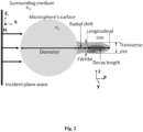
- Photonic nanojets are essentially scattered beams of light with a high-intensity main lobe, a weak subdiffracting waist and a very low divergence angle as shown schematically in Figure 2 where a microsphere illuminated by an optical plane wave generating a spatially restricted optical beam with specific characteristics like longitudinal size, transverse size decay length and a beam radial dimension.
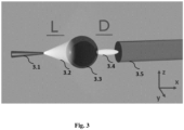
- Figure 3 it is presented the schematic arrangement of the proposed light coupling system of this invention, showing the optical arrangement between a given, specified, nanowire (or NWQD) 3.1 with creates an illuminating light beam 3.2, a properly designed microsphere 3.3 and a given, specified, channel optical waveguide 3.5.
- the separation between the end tip of nanowire (or NWQD) and the adjacent surface of the microsphere is L, while the separation between the surface of the microsphere adjacent to the end of the waveguide, and the waveguide is D.
- the photonic nanojet 3.4 emitted by the microsphere induces proper launching conditions in the vicinity of the adjacent channel optical waveguide leading to proper excitation of the waveguide's supported guided optical modes resulting in efficient coupling of nanowire's emitted light to waveguide's guided light at the fundamental or other higher guided eigenmodes.
- microsphere or an optical dielectric microelement in general
- microsphere or an optical dielectric microelement in general
- photonic nanojets were studied and demonstrated only in the following cases and applications: Enhanced Raman spectroscopy, Photolithography, Nanoparticle detection and manipulation, Enhanced optical absorption in photovoltaics and photodiodes, Laser materials processing and dry laser cleaning, Fluorescence sensing , high -density optical data storage, and novel light transport in linear arrays of microspheres, and not for coupling light to waveguides as described and demonstrated in this invention.
- the invented coupling system and method is based on this excitation of waveguides by the induced photonic nanojet.
- the microsphere does not act as a focussing ball lens that concentrates light into a single point, as it happens in other focussing techniques when using focussing balls of dimensions much greater of 30* ⁇ determined my geometrical optics principles with a well defined optical focal point.
- the photonic jet cannot be described by a single focal point (position and dimension) as it is an electromagnetic beam with certain spatial distribution and light intensity characteristics. Therefore, the design and optimization of coupling through a photonic jet is also entirely different, not trivial, not obvious, and here in this invention is the first time a photonic nanojet is employed for coupling light in an optical waveguide as is demonstrated in specific cases.
- the design of the arrangement of microsphere in between a nanowire (or NWQD) and a specified optical waveguide is based primarily on the appropriate design and selection of: 1) Size (diameter) of the optical microelement (microsphere), 2) Refractive index of optical microelement (microsphere, 3) Distance between the nanowire and the optical microelement (microsphere), 4) Distance between optical microelement (microsphere) and waveguide.
- the selection of the aforementioned parameters depends on the refractive index, geometrical dimensions and waveguiding characteristics of the waveguide, the characteristics of the nanowire and of the refractive index of the surrounding media.
- refractive index measurement can be performed using a refractometer, which analyzes the behavior of light passing through or interacting with the microspheres, or by ellipsometry techniques that measure the changes in the polarization of light as it interacts with the microspheres.
- the method is reliable, robust and tolerant in terms of the aforementioned various imperfections as it is proved practically feasible to accurately determine and achieve the required positions given the current state of the art tools, like nano/micro manipulators for accurate handling of such elements, nanowires, and microspheres.
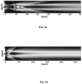
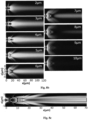
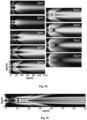
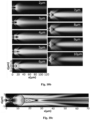
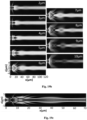
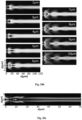
- Figure 4a shows the creation of the photonic nanojet after illumination of the NWQD on the microsphere which is shown as a circle, and the coupling of light in the waveguide for a propagation distance of 70 ⁇ m.
- Figure 4b demonstrates the efficient coupling and lossless propagation of coupled guided light (Transverse Electric - TE mode) for a distance of 300 ⁇ m in the waveguide. Due to dimensions scaling the microsphere is not shown. It should be noted that the color representation and intensity scaling is different between two graphs in order to reveal the electric field propagation details.
- microsphere could be applied also in a number of different types of waveguides such as, Rib Waveguides, Ridge waveguides, Stripe waveguides, and buried waveguides. It can be applied also to a number of types of waveguides fabricated by different means, like: Direct Laser Writing, Reactive Ion Etching (RIE), Electron Beam Lithography, Focussed Ion Beam lithography, In-diffusion, etc.
- RIE Reactive Ion Etching
- Electron Beam Lithography Electron Beam Lithography
- Focussed Ion Beam lithography Focussed Ion Beam lithography
- In-diffusion etc.
- the method solves a very challenging problem and the solution is expected to have a high impact in Quantum technology due to the interest of developing optical computers based on highly customised hybrid optical circuits.
- the invention solves the fundamental problem of coupling light from a nanowire to an optical channel optical waveguide with dissimilar and incompatible waveguiding characteristics.
- the incompatibility of nanowires to low index contrast waveguides is attributed to the dimensions of the nanowire and the resulted mode profile at the end tip of the nanowire which acts as very narrow waveguide.
- the modal waveguiding characteristics depend on the geometric and material characteristics of the nanowire and not of the presence of embedded QD which offers an additional functionality in quantum applications as a single photon source. Therefore this invention provides a solution first, in the generic case of a nanowire coupling which is applied afterwards to various nanowires with or without quantum dots that have significant impact in quantum applications.
- the invention discloses a light coupling system comprising a nanowire (or a nanowire quantum dot), an optical dielectric microelement and a channel optical waveguide, wherein the optical dielectric microelement is placed, between the nanowire and the channel optical waveguide, preferably aligned in the axial direction of the central axis of the channel optical waveguide and the nanowire axis, and the said optical dielectric microelement is configured to enable the coupling and transfer of light from the nanowire (or a NWQD) to the channel optical waveguide.
- such said optical channel waveguides can be related to optical fiber based waveguides, or planar integrated based optical waveguides.
- different optical dielectric microelements with circular or semi-circular cross sections, are used such as a dielectric microsphere, or with shapes as a cylinder, or a half-sphere or a half-cylinder with mesoscale dimensions spanning from 1 ⁇ to 30 ⁇ for operation with light at wavelength equal to ⁇ .
- the optical dielectric microelement is a dielectric microsphere can have a diameter between 2 ⁇ m and 45 ⁇ m and more preferably between 3 ⁇ m and 15 ⁇ m.
- the optical dielectric microelement couples and transfers light from a semiconductor nanowire with one or more quantum dots or without any quantum dots to the channel optical waveguide.
- the channel optical waveguide is fabricated in different material platforms such as in made of Silica, Silica on Silicon, Silicon, Silicon on Insulator, Silicon Nitride, Lithium Niobate, Tantalum Pentoxide, Polymers, or in any combination of them forming hybrid photonic platforms thereof.
- the channel optical waveguides have any of different shape selected from as like: a Ridge waveguide, a Rib Waveguide, a Stripe waveguide, or buried waveguides.
- the channel optical waveguides have been fabricated by any of fabrication means, like Reactive Ion Etching, Focused Ion Beam, Electron Beam Lithography, In-diffusion or, Direct Laser writing or by any combination of them in the same optical integrated circuit or in hybrid optical integrated implementations.
- the nanowire is made by silicon, semiconductor, dielectric or metallic materials than can have also different functionality.
- semiconductor nanowires can be based in different materials like GaAs, InP, GaAs, GaP, GaN, GaAs, GaN, while semiconductor nanowires with embedded quantum dots can be implemented by the following materials combination pairs assigned as [Quantum Dot / Nanowire]: InAs/GaAs, InAsP/InP, AlGaAs/GaAs, GaAsP/GaP, InGaN/GaN, InGaAs/GaAs, AlGaN/GaN.
- the said nanowires can have length between 1 ⁇ m and 20 ⁇ m, diameter from 2 nm to 800 nm, and wavelength of emitting light between 800 nm and 2000 nm.
- Dielectric nanowires can be made by diameter tapering of optical fibers, while metallic can be made by metal wires or by composite metal/glass systems that can be applied in plasmonic applications, with or without embedded quantum dots.
- the channel optical waveguide is fabricated on silica material, or fused silica, or doped silica for refractive index modification such as Germanium doped silica, in a photonics platform like 3-Layer silica-on-silicon structure.
- the channel optical waveguide can have a profile by any of type from: circular, rectangular, orthogonal shape depending on the fabrication process, while the width or diameter of the channel optical waveguide can range between 1 ⁇ m to 10 ⁇ m, and the refractive index difference compared to pure silica can range between 10 -4 and 10 -1 .
- there is a light coupling system wherein the distance between the nanowire and the optical dielectric microelement, or the distance between the microsphere and the waveguide is between 0 ⁇ m and 30 ⁇ m.
- Another aspect of the invention is a method for coupling light from a nanowire to an optical waveguide comprising the steps of i) providing a light coupling system comprised by the [Nanowire - Microsphere - Waveguide] elements according to the aforementioned description ii) ejecting light from a nanowire or a nanowire with one or more quantum dots, iii) illuminating the optical dielectric microelement with the said light in order to produce a photonic nanojet and iv) ejecting the said emitted photonic nanojet into a waveguide or specifically to a channel optical waveguide in order to excite the corresponding waveguide supported (guided) eigenmodes and facilitate light coupling.
- Another aspect of the invention related to the aforementioned method for coupling of a nanowire to an optical waveguide, wherein for a light coupling system with specified nanowire and specified waveguide, it is selected the highest coupling value from the nanowire to the optical waveguide, by ranging the following parameters: 1) Size of the optical microelement, 2) Refractive index of the optical microelement, 3) Distance between the nanowire and the optical microelement, 4) Distance between the optical microelement and the channel optical waveguide, by selecting appropriately the said parameters in order to achieve the maximum light coupling.
- the optical dielectric microelement is a microsphere with refractive index preferably in the range of 1.5 to 2.5, and with diameter between 2 ⁇ m and 45 ⁇ m and more preferably between 3 ⁇ m and 10 ⁇ m.
- Another aspect of the invention is the use of the light coupling system and methods of coupling light in the development and realization of quantum integrated optical circuits for applications in the development of scalable quantum computers, quantum sensors and quantum communications systems.
- the NWQD is a III-V Indium Arsenide Phosphide (InAsP) QD, embodied in an Indium Phosphide (InP) NW, which is a typical case of NWQD.
- the NW is 4 ⁇ m long with a diameter of 200 nm while the taper diameter at the end of the NW is 109nm corresponding to a taper angle of 2°.
- the location of the QD is 200 nm from the NW's base.
- the considered NWQD emits light at 880 nm and therefore all the simulation are considered at this operating wavelength.
- a typical NWQD is schematically shown in Figure 1a,b together with the simulated electric field under excitation.
- the considered NWQD is an indicative case of semiconductor based nanowire with a semiconductor based embedded QD, while in the generic case other nanowires based on different semiconductors systems, or dielectric nanowires or metallic plasmonic nanowires could be considered for light coupling.
- the semiconductor NWQD like the InAsP/InP or InAs/GaAs is in the current state of the art of single photon sources.
- the cylindrical waveguide 1.4 as shown schematically in Figure 1e has a diameter of 3 ⁇ m and has a refractive index of 1.457 which corresponds to a refractive index difference of 5 ⁇ 10 -3 compared to silica with refractive index of 1.452 at 880 nm.
- a refractive index difference of this value provides i) single TE/TM mode operation and ii) moderate confinement thus minimizing the effects due to fabrication of modeling imperfections.
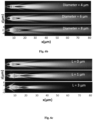
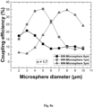
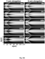
- Figure 5a presents the evaluated light coupling from NWQD to a cylindrical waveguide by simple proximity without the use of a microsphere, for a range of distance L ranging from 0 to 5 ⁇ m.
- Figure 3 illustrates the proposed generic photonic system with the addition of the microsphere 3.3.
- D the distance between the NWQD taper tip and the front microsphere surface.
- D the distance between the NWQD taper tip and the front microsphere surface.
- the invented method is generic and can be applied in various photonic platforms with materials of higher or lower refractive indices than the silica considered in the demonstrated cases. Therefore the refractive indices of the optimal dielectric microspheres can be adjusted to lower or higher refractive indices depending on the specific case.
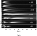
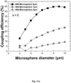
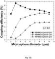
- the addition of the microsphere modifies the spatial characteristics of the emitted light form NWQD light, so it can be tailored to a high degree, by adjusting the refractive index, the diameter and the distance in order to achieve more efficient excitation of the waveguide.
- the photonic nanojet design and customization provides the way for optimal conditions towards efficient coupling to the channel optical waveguide.
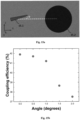
- the coupling efficiency is very sensitive to the relative distance between the nanowire and the microsphere. Small deviations from the optimum design is possible to gradually downgrade the coupling efficiency, however state of the art micropositioning performance (with angular accuracy better than 1° angle and positioning resolution better than 30 nm) can provide adequate accuracy at the nanometer level, avoiding these issues, and ensuring optimal arrangement according to design. Concluding, the coupling efficiency values extracted with the aid of a microsphere are more than an order of magnitude greater than those obtained without the microsphere by just end firing (butt-coupling) the nanowire with the waveguide.
- the second demonstrated case refers to a 3-layer silica-on-silicon planar integrated photonics platform with a middle photosensitive core layer typically from Germanium doped silica glass.
- this photonic platform pictured in Figure 18a consists of a silicon substrate 18.1 followed by a thermally deposited silica layer 18.2, indicatively of 15 ⁇ m thickness for optical isolation.
- the middle layer 18.3 is a photosensitive germanium doped silica layer of typical thickness 3 ⁇ m and on this layer could be defined channel optical waveguides, such as 18.5, by refractive index modification after illumination by ultraviolet laser.
- An over cladding 18.4 of typically 15 ⁇ m protects and optically isolates the circuit.
- Figure 18a A typical configuration employing the invented coupling apparatus with the use of a microsphere is shown in Figure 18a .
- a number of quantum optical circuits have been developed in this platform but with no embedded single photon sources, while this invention demonstrates the feasibility of NWQD integration in this realistic and favorable platform.
- Figure 18b is a schematic diagram showing a magnification of the three dimensional arrangement of the nanowire 18.6, with its generated light beam 18.7 ejected to the microsphere 18.8, which produces the photonic nanojet 18.9, directed to the buried channel optical waveguide 18.10.
- the UV written germanosilicate waveguide is designed as a rectangle with a 3x3 ⁇ m 2 cross-sectional area to ensure the single mode operation.
- Figure 18c shows schematically a 2D diagram with the YZ view, with the geometrical and optical characteristics of a laser written buried channel optical waveguide 18.15, in a structure on silicon substrate 18.11, with silica undercladding 18.12 of 15 ⁇ m, a core layer 18.13 with thickness 3 ⁇ m, and an overcladding 18.14 with thickness 15 ⁇ m.
- Figure 18d shows in a simplified view the optical arrangement in 2D in relation to the 3D view in Figure 18a .
Landscapes
- Physics & Mathematics (AREA)
- General Physics & Mathematics (AREA)
- Optics & Photonics (AREA)
- Chemical & Material Sciences (AREA)
- Engineering & Computer Science (AREA)
- Nanotechnology (AREA)
- Optical Integrated Circuits (AREA)
- Optical Modulation, Optical Deflection, Nonlinear Optics, Optical Demodulation, Optical Logic Elements (AREA)
Applications Claiming Priority (1)
| Application Number | Priority Date | Filing Date | Title |
|---|---|---|---|
| GR20230100588A GR1010889B (el) | 2023-07-17 | 2023-07-17 | Συζευξη φωτος μεταξυ νανοκαλωδιου και οπτικου κυματοδηγου μεσω φωτονικου νανοπιδακα μικροσφαιριδιου |
Publications (1)
| Publication Number | Publication Date |
|---|---|
| EP4495643A1 true EP4495643A1 (de) | 2025-01-22 |
Family
ID=88923866
Family Applications (1)
| Application Number | Title | Priority Date | Filing Date |
|---|---|---|---|
| EP23386114.5A Pending EP4495643A1 (de) | 2023-07-17 | 2023-11-09 | Lichtkopplung zwischen nanodraht und lichtleiter durch photonischen mikrokugel-nanostrahl |
Country Status (3)
| Country | Link |
|---|---|
| EP (1) | EP4495643A1 (de) |
| GR (1) | GR1010889B (de) |
| WO (1) | WO2025016574A1 (de) |
Citations (2)
| Publication number | Priority date | Publication date | Assignee | Title |
|---|---|---|---|---|
| CN105116491A (zh) * | 2015-09-22 | 2015-12-02 | 东南大学 | 一种硅基槽波导集成型光功分器 |
| US20150355227A1 (en) * | 2013-01-11 | 2015-12-10 | Danmarks Tekniske Universitet | Optically guided microdevice comprising a nanowire |
-
2023
- 2023-07-17 GR GR20230100588A patent/GR1010889B/el active IP Right Grant
- 2023-11-09 EP EP23386114.5A patent/EP4495643A1/de active Pending
-
2024
- 2024-04-22 WO PCT/EP2024/060953 patent/WO2025016574A1/en active Pending
Patent Citations (2)
| Publication number | Priority date | Publication date | Assignee | Title |
|---|---|---|---|---|
| US20150355227A1 (en) * | 2013-01-11 | 2015-12-10 | Danmarks Tekniske Universitet | Optically guided microdevice comprising a nanowire |
| CN105116491A (zh) * | 2015-09-22 | 2015-12-02 | 东南大学 | 一种硅基槽波导集成型光功分器 |
Non-Patent Citations (5)
| Title |
|---|
| ALEXANDER HEIFETZ ET AL: "Photonic Nanojets", JOURNAL OF COMPUTATIONAL AND THEORETICAL NANOSCIENCE, vol. 6, no. 9, 1 September 2009 (2009-09-01), US, pages 1979 - 1992, XP055358176, ISSN: 1546-1955, DOI: 10.1166/jctn.2009.1254 * |
| DARAFSHEH ARASH ET AL: "Photonic nanojet properties of dielectric microcylinders", PROCEEDINGS OF SPIE; [PROCEEDINGS OF SPIE ISSN 0277-786X VOLUME 10524], SPIE, US, vol. 10106, 16 February 2017 (2017-02-16), pages 101061U - 101061U, XP060086358, ISBN: 978-1-5106-1533-5, DOI: 10.1117/12.2252758 * |
| MUHAMMAD RODLIN BILLAH ET AL: "Hybrid integration of silicon photonics circuits and InP lasers by photonic wire bonding", ARXIV.ORG, CORNELL UNIVERSITY LIBRARY, 201 OLIN LIBRARY CORNELL UNIVERSITY ITHACA, NY 14853, 9 February 2018 (2018-02-09), XP081134171, DOI: 10.1364/OPTICA.5.000876 * |
| TSINTZOS SIMEON I ET AL: "Design and Fabrication Challenges of Integrated Optical Circuits for Quantum Computing Applications", 2023 23RD INTERNATIONAL CONFERENCE ON TRANSPARENT OPTICAL NETWORKS (ICTON), IEEE, 2 July 2023 (2023-07-02), pages 1 - 4, XP034395036, DOI: 10.1109/ICTON59386.2023.10207396 * |
| YURY P RAKOVICH ET AL: "Mode manipulation in small microsphere systems", TRANSPARENT OPTICAL NETWORKS, 2008. ICTON 2008. 10TH ANNIVERSARY INTERNATIONAL CONFERENCE ON, IEEE, PISCATAWAY, NJ, USA, 22 June 2008 (2008-06-22), pages 23 - 26, XP031306374, ISBN: 978-1-4244-2625-6 * |
Also Published As
| Publication number | Publication date |
|---|---|
| GR20230100588A (el) | 2025-02-11 |
| WO2025016574A1 (en) | 2025-01-23 |
| GR1010889B (el) | 2025-02-26 |
Similar Documents
| Publication | Publication Date | Title |
|---|---|---|
| ar et al. | Design and fabrication of silicon photonic crystal optical waveguides | |
| US11378733B2 (en) | Integrated freeform optical couplers | |
| Olivier et al. | Improved 60 degree bend transmission of submicron-width waveguides defined in two-dimensional photonic crystals | |
| EP1481270A1 (de) | Methode zur führung elektromagnetischer strahlung, speziell in einem integrierten optischen bauteil | |
| Melo et al. | Multiobjective inverse design of solid-state quantum emitter single-photon sources | |
| Tsimvrakidis et al. | Nanowire integration in silica based integrated optical circuits: limitations and challenges towards quantum computing | |
| Fraser et al. | Single-etch silicon nitride grating couplers for multiband applications in quantum and fiber communications | |
| EP4495643A1 (de) | Lichtkopplung zwischen nanodraht und lichtleiter durch photonischen mikrokugel-nanostrahl | |
| US20200355868A1 (en) | Deeply Sub-Wavelength All-Dielectric Waveguide Design and Method for Making the Same | |
| EP1481272A1 (de) | Einrichtung zum beugen eines optischen strahls insbesondere in einer optischen integrierten schaltung | |
| Vitukhnovsky et al. | Three-Dimensional Optical Lithography and Nanoscale Optical Connectors | |
| Tsintzos et al. | Enabling light coupling between nanowires and low refractive index contrast optical waveguides towards scalable quantum circuits | |
| Tsintzos et al. | Design and fabrication challenges of integrated optical circuits for quantum computing applications | |
| Ren et al. | Digitized adjoint method for inverse design of digital nanophotonic devices | |
| Nawi et al. | Discrepancies in the free spectral range (FSR) of one-dimensional (1D) photonic crystal/photonic wire coupled-cavities | |
| Gan et al. | Designs and experiments on infrared two-dimensional silicon photonic crystal slab devices | |
| Digaum | Fabrication and characterization of spatially-variant self-collimating photonic crystals | |
| Gan et al. | Two‐dimensional air‐bridged silicon photonic crystal slab devices | |
| Al Maruf et al. | High Efficiency Fiber-Coupled Single-Photon Source Based on Quantum Dot Embedded in a Semiconductor Nanowire | |
| Riziotis et al. | Nanowire Integration in Silica Based Integrated Optical Circuits: Limitations and Challenges Towards Quantum Computing | |
| Chau et al. | Efficient mode coupling technique between photonic crystal heterostructure waveguide and silica waveguides | |
| Wuest et al. | Near-field optical microscopy of light propagation through photonic crystal waveguide tapers | |
| Wang et al. | Nanopatterned Photonics on Probe: Modeling, Simulations, and Applications for Near-Field Light Manipulation | |
| Krauss | Planar photonic crystal microcircuit elements | |
| Lipson | High-confinement nanophotonic structures on chip |
Legal Events
| Date | Code | Title | Description |
|---|---|---|---|
| STAA | Information on the status of an ep patent application or granted ep patent |
Free format text: STATUS: UNKNOWN |
|
| PUAI | Public reference made under article 153(3) epc to a published international application that has entered the european phase |
Free format text: ORIGINAL CODE: 0009012 |
|
| STAA | Information on the status of an ep patent application or granted ep patent |
Free format text: STATUS: THE APPLICATION HAS BEEN PUBLISHED |
|
| AK | Designated contracting states |
Kind code of ref document: A1 Designated state(s): AL AT BE BG CH CY CZ DE DK EE ES FI FR GB GR HR HU IE IS IT LI LT LU LV MC ME MK MT NL NO PL PT RO RS SE SI SK SM TR |
|
| STAA | Information on the status of an ep patent application or granted ep patent |
Free format text: STATUS: REQUEST FOR EXAMINATION WAS MADE |
|
| 17P | Request for examination filed |
Effective date: 20250722 |