EP4492811A1 - Photoelectric conversion circuit, and photoelectric conversion device - Google Patents
Photoelectric conversion circuit, and photoelectric conversion device Download PDFInfo
- Publication number
- EP4492811A1 EP4492811A1 EP23766524.5A EP23766524A EP4492811A1 EP 4492811 A1 EP4492811 A1 EP 4492811A1 EP 23766524 A EP23766524 A EP 23766524A EP 4492811 A1 EP4492811 A1 EP 4492811A1
- Authority
- EP
- European Patent Office
- Prior art keywords
- exposure
- unit
- transistor
- charges
- photoelectric conversion
- Prior art date
- Legal status (The legal status is an assumption and is not a legal conclusion. Google has not performed a legal analysis and makes no representation as to the accuracy of the status listed.)
- Pending
Links
Images



Classifications
-
- H—ELECTRICITY
- H04—ELECTRIC COMMUNICATION TECHNIQUE
- H04N—PICTORIAL COMMUNICATION, e.g. TELEVISION
- H04N25/00—Circuitry of solid-state image sensors [SSIS]; Control thereof
- H04N25/70—SSIS architectures; Circuits associated therewith
- H04N25/703—SSIS architectures incorporating pixels for producing signals other than image signals
- H04N25/705—Pixels for depth measurement, e.g. RGBZ
-
- G—PHYSICS
- G01—MEASURING; TESTING
- G01S—RADIO DIRECTION-FINDING; RADIO NAVIGATION; DETERMINING DISTANCE OR VELOCITY BY USE OF RADIO WAVES; LOCATING OR PRESENCE-DETECTING BY USE OF THE REFLECTION OR RERADIATION OF RADIO WAVES; ANALOGOUS ARRANGEMENTS USING OTHER WAVES
- G01S17/00—Systems using the reflection or reradiation of electromagnetic waves other than radio waves, e.g. lidar systems
- G01S17/02—Systems using the reflection of electromagnetic waves other than radio waves
- G01S17/06—Systems determining position data of a target
- G01S17/08—Systems determining position data of a target for measuring distance only
- G01S17/10—Systems determining position data of a target for measuring distance only using transmission of interrupted, pulse-modulated waves
- G01S17/18—Systems determining position data of a target for measuring distance only using transmission of interrupted, pulse-modulated waves wherein range gates are used
-
- G—PHYSICS
- G01—MEASURING; TESTING
- G01S—RADIO DIRECTION-FINDING; RADIO NAVIGATION; DETERMINING DISTANCE OR VELOCITY BY USE OF RADIO WAVES; LOCATING OR PRESENCE-DETECTING BY USE OF THE REFLECTION OR RERADIATION OF RADIO WAVES; ANALOGOUS ARRANGEMENTS USING OTHER WAVES
- G01S17/00—Systems using the reflection or reradiation of electromagnetic waves other than radio waves, e.g. lidar systems
- G01S17/88—Lidar systems specially adapted for specific applications
- G01S17/89—Lidar systems specially adapted for specific applications for mapping or imaging
- G01S17/894—Three-dimensional [3D] imaging with simultaneous measurement of time-of-flight at a two-dimensional [2D] array of receiver pixels, e.g. time-of-flight cameras or flash lidar
-
- G—PHYSICS
- G01—MEASURING; TESTING
- G01S—RADIO DIRECTION-FINDING; RADIO NAVIGATION; DETERMINING DISTANCE OR VELOCITY BY USE OF RADIO WAVES; LOCATING OR PRESENCE-DETECTING BY USE OF THE REFLECTION OR RERADIATION OF RADIO WAVES; ANALOGOUS ARRANGEMENTS USING OTHER WAVES
- G01S7/00—Details of systems according to groups G01S13/00, G01S15/00, G01S17/00
- G01S7/48—Details of systems according to groups G01S13/00, G01S15/00, G01S17/00 of systems according to group G01S17/00
- G01S7/483—Details of pulse systems
- G01S7/486—Receivers
- G01S7/4861—Circuits for detection, sampling, integration or read-out
- G01S7/4863—Detector arrays, e.g. charge-transfer gates
-
- G—PHYSICS
- G01—MEASURING; TESTING
- G01S—RADIO DIRECTION-FINDING; RADIO NAVIGATION; DETERMINING DISTANCE OR VELOCITY BY USE OF RADIO WAVES; LOCATING OR PRESENCE-DETECTING BY USE OF THE REFLECTION OR RERADIATION OF RADIO WAVES; ANALOGOUS ARRANGEMENTS USING OTHER WAVES
- G01S7/00—Details of systems according to groups G01S13/00, G01S15/00, G01S17/00
- G01S7/48—Details of systems according to groups G01S13/00, G01S15/00, G01S17/00 of systems according to group G01S17/00
- G01S7/497—Means for monitoring or calibrating
-
- H—ELECTRICITY
- H04—ELECTRIC COMMUNICATION TECHNIQUE
- H04N—PICTORIAL COMMUNICATION, e.g. TELEVISION
- H04N25/00—Circuitry of solid-state image sensors [SSIS]; Control thereof
- H04N25/70—SSIS architectures; Circuits associated therewith
- H04N25/76—Addressed sensors, e.g. MOS or CMOS sensors
- H04N25/77—Pixel circuitry, e.g. memories, A/D converters, pixel amplifiers, shared circuits or shared components
Definitions
- the present disclosure relates to a photoelectric conversion circuit and a photoelectric conversion device.
- one aspect of the disclosure is a photoelectric conversion circuit including a light receiving element that outputs charges corresponding to an amount of exposure to a predetermined wiring line, an output circuit that, when an instruction signal is input, outputs charges corresponding to a period during which the instruction signal is input to the predetermined wiring line, a plurality of charge storage units, and a transfer circuit that transfers the charges output to the predetermined wiring line to each of the plurality of charge storage units.
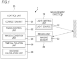
- FIG. 1 is a diagram showing a configuration of a measuring device 1.
- the timing control unit 32 controls the light emission timing of the light emitting unit 10 and the exposure timing of the imaging unit 20. The light emission timing and the exposure timing will be described later.
- the image acquisition unit 34 acquires image data from the imaging sensor 22 of the imaging unit 20.
- the image acquisition unit 34 also includes a memory (not shown) that stores the acquired image data.
- the time calculation unit 36 calculates an arrival time from when the light source 12 of the light emitting unit 10 emits light to when reflected light reaches the imaging sensor 22 of the imaging unit 20, that is, a flight time of light: ToF.
- FIG. 2 is a diagram showing a configuration of the imaging sensor 22 in the present embodiment.
- the imaging sensor 22 captures an image of an imaging target in response to an instruction from the control unit 30, and outputs image data obtained by capturing the image to the image acquisition unit 34 of the control unit 30.
- the value of each pixel (pixel data) that constitutes the image data indicates a signal value corresponding to the amount of exposure.
- the imaging sensor 22 has a plurality of pixels 221 disposed two-dimensionally (for example, 640 ⁇ 480).
- Each of the pixels 221 includes a light receiving element D1, a transistor SPD, a transistor PDR, an output circuit 50, a transfer circuit 60, signal readout units RU1 to RU4, and signal conversion units SO1 to SO4.
- the imaging sensor 22 (pixel 221) corresponds to a "photoelectric conversion circuit”.
- each transistor used in the imaging sensor 22 is, for example, an N-type MOSFET, and the turn-on/turn-off of each transistor is controlled by the control unit 30.
- the light receiving element D1 is an element (such as a photodiode) that generates charges corresponding to the amount of exposure.
- the light receiving element D1 outputs the generated charges to a wiring line L1 via the transistor SPD.
- the wiring line L1 corresponds to a "prescribed wiring line”.
- the transistor PDR is an element that discharges charges of the light receiving element D1, and is connected in parallel to the light receiving element D1.
- the transistor PDR corresponds to a "third switch”.
- the signal conversion unit SO1 outputs a signal value corresponding to the charges stored in the charge storage unit CS1 by selecting the select transistor SL1 of the signal readout unit RU1.
- the signal conversion unit SO1 includes an amplifier circuit ZF1 that amplifies the output of the signal readout unit RU1, and an A/D conversion circuit HK1 that converts an analog signal output from the amplifier circuit ZF1 into a digital signal.
- the signal conversion unit SO1 then converts the charges stored in the charge storage unit CS1 (the amount of exposure during the exposure period) into a signal value (digital signal) corresponding to the charges and outputs the signal value to the image acquisition unit 34 of the control unit 30.
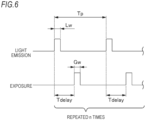
- FIG. 6 is a diagram showing a light emission timing and an exposure timing.
- FIG. 7 is a diagram showing creation of a distance image by indirect ToF. As described above, during measurement, control is performed such that the transistor SPD is turned on and transistors SCS and PDR and reset transistors RT1 to RT4 are turned off.
- Light emission and exposure are repeated a plurality of times at a cycle Tp shown in FIG. 6 . This is for storage of charges in the imaging sensor 22.
- the farther a region to be measured the larger the number of repetitions n is set. This is because reflected light becomes weaker the farther the region.
- a multi-tap (specifically, 4-tap) CMOS image sensor is used as the imaging sensor 22.
- four exposure periods can be set for one light emission, and four regions can be measured. That is, four range images are obtained through one imaging.
- the number of range images (four in this case) obtained through one imaging may be referred to as "subframes”.
- a plurality of regions (four regions in this case) measured through one imaging may be referred to as a "zone".
- the imaging sensor 22 is not limited to a 4-tap CMOS image sensor.
- control unit 30 causes the light emitting unit 10 to emit light at a cycle Tp (see FIG. 6 ) and controls the exposure timing of the imaging unit 20 in accordance with the light emission timing.
- image acquisition unit 34 acquires an image (image data) captured by the imaging unit 20 at each exposure timing.
- the control unit 30 acquires an image of a zone 1 (regions 1 to 4). That is, the timing control unit 32 causes the imaging sensor 22 of the imaging unit 20 to perform exposure for each pixel of the image during exposure periods 1 to 4 (see FIG. 8 ) delayed from the light emission timing.
- the timing control unit 32 repeatedly performs exposure at each cycle Tp, and stores charges in the charge storage units CS1 to CS4.
- the control unit 30 acquires an image of a zone 2 (regions 5 to 8).
- the control unit 30 then writes the image data of the range images (subframes) of the regions 5 to 8 to the image memory of the image acquisition unit 34.
- a delay time Tdelay for the light emission timing in the zone 2 (regions 5 to 8) is set to be longer than that of the zone 1 (regions 1 to 4).
- the number of repetitions is set to be larger as a region to be measured becomes farther.
- light emitting pulses are separate in the regions 4 and 5
- the exposure periods of the regions 4 and 5 are continuous when the light emitting pulse is used as a reference. In this manner, continuous exposure periods are not limited to those constituted by only exposure periods with the same light emission timing, but may also include exposure periods with different light emission timings.
- images up to the region N are acquired.
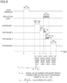
- FIG. 8 is a diagram showing a relationship between light emission and exposure in the case of four taps.
- the pulse width of the light emitting pulse is Lw.
- the pulse width of reflected light is also Lw.
- exposures 1 to 4 are set.
- the width of each of the exposure periods (exposure widths) of the exposures 1 to 4 is the same as the pulse width Lw of the light emitting pulse.
- the exposure period is a period during which the level of exposure in FIG. 8 is a high level (H level).
- the H/L levels of the exposures 1 to 4 indicate turn-on/turn-off of the transfer transistors G1 to G4 in FIG. 2 .
- the reflected light may arrive in a period different from the exposure period 2 and the exposure period 3, and for example, the reflected light may be exposed in the exposure period 1 and the exposure period 2.
- the exposure period 3 corresponding to a region (region 3) next to the region 2 is set for the exposure 3.
- the pixel 221 of the imaging sensor 22 acquires a signal value S 3 corresponding to the amount of exposure of the reflected light in the exposure period 3.
- the exposure period 4 corresponding to a region (region 4) next to the region 3 is set for the exposure 4.
- reflected light is not exposed in the exposure period 4, and thus no charges are stored in the charge storage unit CS4 of the pixel 221 of the imaging sensor 22. That is, a signal value S 4 acquired in the exposure period 4 is zero.
- signal values S i (here, S 1 to S 4 ) become signal values corresponding to charges (corresponding to the amount of exposure) stored by repeating the exposure by the number of repetitions n.
- the signal conversion units SO1 to SO4 of the pixels 221 of the imaging sensor 22 output the signal values S 1 to S 4 corresponding to the charges stored in the charge storage units CS1 to CS4.
- the signal values S 1 to S 4 correspond to the values of pixels (pixel data) that constitute the image data of the images (range images) of the regions 1 to 4, respectively.
- the image acquisition unit 34 of the control unit 30 acquires the signal values S 1 to S 4 (signal values corresponding to the charges in the charge storage units CS1 to CS4) of the pixels 221 from the imaging sensor 22. Thereby, the image acquisition unit 34 acquires the image data of the regions 1 to 4. Similarly, the image acquisition unit 34 acquires images up to the region N (images of all regions).
- the time calculation unit 36 of the control unit 30 calculates an arrival time Tx of reflected light. Specifically, first, the time calculation unit 36 specifies a signal value S of exposure of the reflected light from among the signal values S 1 to S 4 (signal values S 1 to S N ). For example, the time calculation unit 36 specifies a signal value with the largest amount of exposure which is a signal corresponding to two consecutive exposure periods. For example, when a signal value corresponding to an exposure period i in which the exposure of the reflected light is started is set to be S i , two signal values S i and S i + 1 are specified.
- signal values S 2 and S 3 correspond to the signal values S i and S i + 1 of the exposure of the reflected light.
- the time calculation unit 36 calculates a flight time of light (hereinafter also referred to as an arrival time) Tx according to the following Formula (1) by using the signal values S i and S i+1 .
- Tx T i + 1 ⁇ Lw ⁇ S i / S i + S i + 1
- the distance calculation unit 38 calculates the distance L to the object by Formula (2).
- the imaging sensor 22 and the measuring device 1 according to the present embodiment have been described above.
- the imaging sensor 22 includes the light receiving element D1, the output circuit 50, four charge storage units CS1 to CS4, and the transfer circuit 60.
- the light receiving element D1 outputs charges corresponding to the amount of exposure to the wiring line L1.
- the output circuit 50 receives an input of a signal (H-level signal Sa) for instructing calibration from the control unit 30, the output circuit 50 outputs charges corresponding to a period during which the signal is input to the wiring line L1.
- the transfer circuit 60 transfers the charges output to the wiring line L1 to each of the four charge storage units CS1 to CS4. Thereby, it is possible to output charges (current) for calibration from the output circuit 50, and thus variations can be corrected without using dedicated equipment.
- the output circuit 50 also includes the current source 52 and the transistor SCS.
- the transistor SCS is provided between the current source 52 and the wiring line L1, and is turned on based on a command signal from the control unit 30 and turned off based on a stop signal. Thereby, it is possible to control the supply of charges (current) from the current source 52 to the wiring line L1.
- the current source 52A of the output circuit 50A includes the resistor R1 having one end to which a voltage VS is applied, and the capacitor CA connected to the other end of the resistor R1.
- the transistor SCS is connected to a node N1 to which the resistor R1 and the capacitor CA are connected.
- the imaging sensor 22 includes the transistor SPD provided between the light receiving element D1 and the wiring line L1. Thereby, it is possible to perform calibration at a desired timing.
Landscapes
- Engineering & Computer Science (AREA)
- Physics & Mathematics (AREA)
- Computer Networks & Wireless Communication (AREA)
- General Physics & Mathematics (AREA)
- Radar, Positioning & Navigation (AREA)
- Remote Sensing (AREA)
- Electromagnetism (AREA)
- Multimedia (AREA)
- Signal Processing (AREA)
- Optical Radar Systems And Details Thereof (AREA)
Abstract
Description
- The present disclosure relates to a photoelectric conversion circuit and a photoelectric conversion device.
- For example, as an indirect Time of Flight (ToF) type measuring device, a measuring device equipped with an imaging sensor that converts light into an electrical signal is known. In addition,
Patent Document 1 discloses a measuring device having a multi-tap configuration in which a plurality of charge storage units are provided, and electric charges are distributed and stored in each of the charge storage units. - Patent Document 1:
JP2021-25833A - In the case of a multi-tap, variations may occur in distribution characteristics between taps. In the related art, dedicated equipment such as a brightness box is required to correct such variations between taps. For this reason, the timing and environment for correcting the variations are limited.
- An object of the present disclosure is to correct variations without using dedicated equipment.
- In order to achieve the above-described object, one aspect of the disclosure is a photoelectric conversion circuit including a light receiving element that outputs charges corresponding to an amount of exposure to a predetermined wiring line, an output circuit that, when an instruction signal is input, outputs charges corresponding to a period during which the instruction signal is input to the predetermined wiring line, a plurality of charge storage units, and a transfer circuit that transfers the charges output to the predetermined wiring line to each of the plurality of charge storage units.
- According to the present disclosure, it is possible to correct variations without using dedicated equipment.
-
-
FIG. 1 is a diagram showing a configuration of ameasurement device 1. -
FIG. 2 is a diagram showing a configuration of animaging sensor 22 according to the present embodiment. -
FIG. 3 is a flow diagram showing calibration. -
FIG. 4 is a diagram showing a modification example of an output circuit. -
FIG. 5 is a diagram showing a comparative example of correction of variations between taps. -
FIG. 6 is a diagram showing a light emission timing and an exposure timing. -
FIG. 7 is a diagram showing creation of a distance image by indirect ToF. -
FIG. 8 is a diagram showing a relationship between light emission and exposure in the case of four taps. - Hereinafter, an embodiment for implementing the present disclosure will be described with reference to the drawings. In the following description, the same or similar components may be denoted by common reference numerals, and repeated descriptions may be omitted.
-
FIG. 1 is a diagram showing a configuration of ameasuring device 1. - The
measuring device 1 shown inFIG. 1 is a Time of Flight (ToF) type device that measures a distance to an object in front. In the present embodiment, an indirect ToF type camera (hereinafter referred to as a ToF camera) is used. Such ameasuring device 1 can eliminate the effects of fog and rain and can perform imaging and measurement even in bad weather. Themeasuring device 1 is provided, for example, in a vehicle. - As shown in
FIG. 1 , themeasuring device 1 includes alight emitting unit 10, animaging unit 20, and acontrol unit 30. In the present embodiment, themeasuring device 1 corresponds to a "photoelectric conversion device". - The
light emitting unit 10 can emit (project) light into a space to be imaged (measurement area). Thelight emitting unit 10 is controlled such that it emits light in response to instructions from thecontrol unit 30. Thelight emitting unit 10 includes alight source 12 and a projection optical system (not shown) that emits light generated by thelight source 12. - The
light source 12 is a light source including a light emitting element (not shown). Thelight source 12 emits pulse-like laser light under the control of thecontrol unit 30. Hereinafter, this pulse-like light (pulsed light) is also referred to as a light emitting pulse. Thelight source 12 will be described in detail later. - The imaging unit 20 (ToF camera) performs imaging on the basis of exposure of light reflected by an object for distance measurement. The
imaging unit 20 includes animaging sensor 22 and an exposure optical system (lens, and the like: not shown) that guides incident (exposed) light to theimaging sensor 22. Theimaging sensor 22 will be described in detail later. - In the present embodiment, the light emission of the
light emitting unit 10 and the exposure operation of theimaging unit 20 are controlled by thecontrol unit 30, but the disclosure is not limited thereto. For example, thelight emitting unit 10 and theimaging unit 20 may be provided with atiming control unit 32, which will be described later, so that light emission and exposure operations can be performed without going through thecontrol unit 30. - The
control unit 30 controls themeasuring device 1. Thecontrol unit 30 is realized by a hardware configuration such as elements and circuits such as a memory and a CPU. Thecontrol unit 30 realizes a predetermined function by causing the CPU to execute a program stored in the memory. Thecontrol unit 30 is not limited to being realized by software processing execution by the memory and the CPU. For example, thecontrol unit 30 may be realized by hardware such as an ASIC and an FPGA.FIG. 1 shows various functions realized by thecontrol unit 30. Thecontrol unit 30 includes acorrection unit 31, atiming control unit 32, animage acquisition unit 34, atime calculation unit 36, and adistance calculation unit 38. - The
correction unit 31 controls theimaging sensor 22 of theimaging unit 20 to execute calibration and correct variations between taps of theimaging sensor 22. In the present embodiment, the tap corresponds to a "charge storage unit". Thecorrection unit 31 also transmits a signal Sa (seeFIG. 2 ) for instructing theimaging sensor 22 to execute and stop calibration, as will be described later. The calibration processing performed by thecorrection unit 31 will be described later. - The
timing control unit 32 controls the light emission timing of thelight emitting unit 10 and the exposure timing of theimaging unit 20. The light emission timing and the exposure timing will be described later. - The
image acquisition unit 34 acquires image data from theimaging sensor 22 of theimaging unit 20. Theimage acquisition unit 34 also includes a memory (not shown) that stores the acquired image data. - The
time calculation unit 36 calculates an arrival time from when thelight source 12 of thelight emitting unit 10 emits light to when reflected light reaches theimaging sensor 22 of theimaging unit 20, that is, a flight time of light: ToF. - The
distance calculation unit 38 calculates a distance on the basis of the exposure result of theimaging sensor 22 and the arrival time of light. As will be described below, a distance image can be acquired by calculating a distance for each pixel. -
FIG. 2 is a diagram showing a configuration of theimaging sensor 22 in the present embodiment. - The
imaging sensor 22 captures an image of an imaging target in response to an instruction from thecontrol unit 30, and outputs image data obtained by capturing the image to theimage acquisition unit 34 of thecontrol unit 30. The value of each pixel (pixel data) that constitutes the image data indicates a signal value corresponding to the amount of exposure. - As shown in
FIG. 2 , theimaging sensor 22 has a plurality ofpixels 221 disposed two-dimensionally (for example, 640 × 480). Each of thepixels 221 includes a light receiving element D1, a transistor SPD, a transistor PDR, anoutput circuit 50, atransfer circuit 60, signal readout units RU1 to RU4, and signal conversion units SO1 to SO4. In the present embodiment, the imaging sensor 22 (pixel 221) corresponds to a "photoelectric conversion circuit". In addition, each transistor used in theimaging sensor 22 is, for example, an N-type MOSFET, and the turn-on/turn-off of each transistor is controlled by thecontrol unit 30. - The light receiving element D1 is an element (such as a photodiode) that generates charges corresponding to the amount of exposure. In addition, the light receiving element D1 outputs the generated charges to a wiring line L1 via the transistor SPD. The wiring line L1 corresponds to a "prescribed wiring line".
- The transistor SPD has the function of a switch that switches between connection and disconnection between the light receiving element D1 and the wiring line L1, and is provided between the wiring line L1 and the light receiving element D1. The transistor SPD corresponds to a "second switch".
- The transistor PDR is an element that discharges charges of the light receiving element D1, and is connected in parallel to the light receiving element D1. The transistor PDR corresponds to a "third switch".
- The
output circuit 50 is a circuit that outputs charges to the wiring line L1 in accordance with a period during which a signal Sa (in this example, an H-level signal Sa) for instructing the execution of calibration is input from the control unit 30 (more specifically, the correction unit 31). - The
output circuit 50 in the present embodiment includes acurrent source 52 that generates a predetermined constant current, and a transistor SCS. - The transistor SCS is provided between the
current source 52 and the wiring line L1, and functions as a switch that is turned on or off on the basis of the level of the signal Sa. Specifically, the transistor SCS is turned on when the signal Sa is at an H level. When the transistor SCS is turned on, charges generated by thecurrent source 52 are output to the wiring line L1. In addition, the transistor SCS is turned off when the signal Sa is at an L level. When the transistor SCS is turned off, thecurrent source 52 is disconnected from the wiring line L1. That is, charges generated by thecurrent source 52 are no longer output to the wiring line L1. The transistor SCS corresponds to a "first switch". - Further, in the present embodiment, a signal for turning on the transistor SCS (H-level signal Sa) corresponds to an "instruction signal", and a signal for turning off the transistor SCS (L-level signal Sa) corresponds to a "stop signal". The
output circuit 50 in the present embodiment includes thecurrent source 52 and the transistor SCS, but is not limited thereto. For example, as theoutput circuit 50, a current mirror circuit that generates a current (constant current) on the basis of the H-level signal Sa and stops generating a current on the basis of the L-level signal Sa may be used. - The
transfer circuit 60 transfers the charges on the wiring line L1 to each of the signal readout units RU1 to RU4 (more specifically, the charge storage units CS1 to CS4). Thetransfer circuit 60 includes four transistors (transfer transistors G1 to G4) connected in parallel to the wiring line L1. The transfer transistor G1 is connected to the charge storage unit CS1 of the signal readout unit RU1, and when the transfer transistor G1 is turned on, the transfer transistor G1 transfers the charges on the wiring line L1 to the chargestorage unit CS 1. Similarly, the transfer transistors G2 to G4 are connected to the charge storage units CS2 to CS4, respectively, and transfer the charges on the wiring line L1 to the charge storage units CS2 to CS4. - Here, the charges on the wiring line L1 are charges from the
current source 52 when the transistor SCS is turned on and the transistor SPD is turned off. In addition, when the transistor SCS is turned off and the transistor SPD is turned on, the charges are charges from the light receiving element D1. Thecontrol unit 30 performs control so that the transfer transistors G1 to G4 and the transistors SCS, SPD, and PDR are turned on or off. - The signal readout unit RU1 includes a charge storage unit CS1, a reset transistor RT1, a source follower transistor SF1, and a select transistor SL1.
- The charge storage unit CS1 is formed by a storage capacitor C1 (capacitor) for storing charges from the wiring line L1, and is generally referred to as a floating diffusion (FD). During measurement by indirect ToF, charges are repeatedly stored in the charge storage unit CS1 in accordance with the number of repetitions n. The charges stored in the charge storage unit CS1 correspond to the amount of exposure to which the light receiving element D1 is exposed during the corresponding exposure period. In the present embodiment, the charge storage unit CS1 (floating diffusion FD1) is constituted using the storage capacitor C1, but a configuration without the storage capacitor C1 (capacitor), for example, a configuration with only parasitic capacitance may be adopted.
- The reset transistor RT1 is an element (transistor) for discharging charges stored in the charge storage unit CS1, that is, resetting the charges to a reset voltage VRT. The source follower transistor SF1 and the select transistor SL1 read out the charges stored in the charge storage unit CS1 (output the charges to the signal conversion section SO1) on the basis of a selection signal (row selection signal) applied to a gate of the select transistor SL1. Each of the signal readout sections RU2 to RU4 has the same configuration as that of the signal readout section RU1, and thus the description thereof is omitted.
- The signal conversion unit SO1 outputs a signal value corresponding to the charges stored in the charge storage unit CS1 by selecting the select transistor SL1 of the signal readout unit RU1. As shown in
FIG. 2 , the signal conversion unit SO1 includes an amplifier circuit ZF1 that amplifies the output of the signal readout unit RU1, and an A/D conversion circuit HK1 that converts an analog signal output from the amplifier circuit ZF1 into a digital signal. The signal conversion unit SO1 then converts the charges stored in the charge storage unit CS1 (the amount of exposure during the exposure period) into a signal value (digital signal) corresponding to the charges and outputs the signal value to theimage acquisition unit 34 of thecontrol unit 30. The signal value (digital signal) based on the charges stored in the charge storage unit CS1 is a signal value corresponding to the amount of exposure during the exposure period. Each of the signal conversion units SO2 to SO4 has the same configuration as that of the signal conversion unit SO1, and thus the description thereof is omitted. - By using such a 4-
tap imaging sensor 22, it is possible to measure four regions through one imaging (described later). That is, four range images are obtained through one imaging. The number of range images (four in this case) obtained through one imaging may be referred to as "subframes". In addition, the plurality of regions (four in this case) measured through one imaging may be referred to as a "zone". - Incidentally, in the case of the
multi-tap imaging sensor 22, variations may occur in the distribution characteristics between the taps due to the characteristics of the transfer circuit 60 (transfer transistors G1 to G4) and the charge storage units CS, and the like. In themeasuring device 1 according to the present embodiment, it is possible to perform calibration using theoutput circuit 50 before the actual measurement. -
FIG. 3 is a flow diagram showing calibration. In the present embodiment, the control unit 30 (in this example, the correction unit 31) performs the calibration by controlling the turn-on/turn-off of each transistor (transistors SCS, SPD, and the like) of thepixel 221 of theimaging sensor 22. - First, the
correction unit 31 turns off the transistors SPD and SCS, and turns on the reset transistors RT1 to RT4 (S101). Thereby, the light receiving element D1 and thecurrent source 52 are disconnected from the wiring line L1, and the charges in the charge storage units CS1 to CS4 (floating diffusions FD1 to FD4) are reset. - Next, the
correction unit 31 outputs an H-level signal Sa indicating calibration to turn on the transistor SCS. Furthermore, thecorrection unit 31 applies a predetermined voltage to a target transistor among the transfer transistors G1 to G4 of thetransfer circuit 60 to turn on the transistor for a predetermined period and turn off the other transistors (S102). Thereby, the charges of thecurrent source 52 are transferred to the corresponding charge storage unit CS via the wiring line L1 and the target transistor. - When the process of step S102 has not been performed for all of the transfer transistors G1 to G4 (NO in S103), the processing returns to step S102, and the
correction unit 31 switches the target transistor and performs the same processing. In this manner, a target transistor is sequentially switched to perform the process of step S102, and thus charges are stored in the charge storage units CS (charge storage units CS1 to CS4). - When the process of step S102 has been performed for all of the transfer transistors G1 to G4 (YES in S103), the
correction unit 31 acquires signal values corresponding to the charges stored in the charge storage units CS (charge storage units CS1 to CS4). Then, thecorrection unit 31 determines whether the voltages (voltages V1 to V4) of the charge (capacitance) storage units CS1 to CS4 are substantially the same on the basis of the signal values (S104). The voltages V1 to V4 correspond to the charges (charges corresponding to turn-on periods) transferred from thecurrent source 52 to the charge storage units CS1 to CS4 during the turn-on periods of the transfer transistors G1 to G4, respectively. - Here, "substantially the same" means that the voltages V1 to V4 fall in a predetermined range from a predetermined voltage Vref (a voltage determined in advance by the charges, the turn-on periods, and the capacitance), for example, in a range of ± 5% of the Vref level.
- When the voltages V1 to V4 are not substantially the same (NO in S104), the
control unit 30 adjusts gate voltages of the transfer transistors G1 to G4 (S105). For example, thecontrol unit 30 increases the gate voltage of the transfer transistor G corresponding to the charge storage unit CS with a low voltage so that the other voltages match the largest voltage among the voltages V1 to V4. Then, the processing returns to step S102, and thecontrol unit 30 performs calibration again. - In step S104, when the voltages V1 to V4 are substantially the same (YES in S104), the
correction unit 31 stores the gate voltages of the transfer transistors G1 to G4 in a memory or the like (S106). Thereafter, when the actual measurement is performed, thecontrol unit 30 uses these gate voltages, that is, applies them to the gates of the corresponding transfer transistors. - Next, the
correction unit 31 sets the signal Sa to an L level to turn off the transistor SCS. Thereby, thecurrent source 52 is disconnected from the wiring line L1. In addition, thecorrection unit 31 turns on the transistor PDR and the reset transistors RT1 to RT4. Thereby, the charges of the light receiving element D1 and the charge storage units CS1 to CS4 are discharged (S107). Thereafter, the control unit 30 (correction unit 31) turns on the transistor SPD and turns off the transistor PDR and the reset transistors RT1 to RT4 to start measurement (S108). -
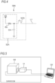
FIG. 4 is a diagram showing a modification example of an output circuit (output circuit 50A). - The
output circuit 50A according to the modification example includes acurrent source 52A. Thecurrent source 52A includes a resistor R1 and a capacitor CA. - A certain voltage VS is applied to one end of the resistor R1. One terminal of the capacitor CA is connected to the other end of the resistor R1, and the other terminal is grounded. In addition, a transistor SCS is connected to a connection point (node) between the capacitor CA and the resistor R1.
- The capacitance of the capacitor CA and the value of the voltage VS are set such that the charges of the
current source 52A (capacitor CA) are not depleted due to the charges transferred to the corresponding charge storage unit CS during a period when each transfer transistor of thetransfer circuit 60 is turned on. - Also in this modification example, the control of the turn-on/turn-off of the transistor SCS during calibration is the same as in the previous embodiment.
- In this modification example, the
output circuit 50A (current source 52A) can be configured simply without using a complex circuit. -
FIG. 5 is a diagram showing a comparative example of correction of variations between taps. - A measuring
device 1A according to this comparative example differs from the measuringdevice 1 of the present embodiment in that theimaging sensor 22 is not provided with anoutput circuit 50. In this comparative example, before themeasuring device 1A is shipped from the factory, theimaging sensor 22 of themeasuring device 1A is accommodated in aluminance box 100 with a designated illuminance as shown inFIG. 5 . Then, the sensitivity of each tap (each charge storage unit CS) with respect to irradiation with a designated illuminance is measured by acontrol computer 120. Theluminance box 100 irradiates themeasuring device 1A (or the imaging sensor 22) with uniform light with a designated illuminance. A voltage applied to the gates of the transfer transistors G1 to G4 of thetransfer circuit 60 is adjusted such that the sensitivity with respect to this illuminance is uniform for each tap. - In the case of this comparative example, dedicated equipment (
brightness box 100 and control computer 120) is required. For this reason, there is a concern the efficiency of shipping tests may be reduced. Furthermore, it is not possible to correct variations between taps due to temperature changes or deterioration with time. - On the other hand, in the
measurement device 1 of the present embodiment, calibration can be performed using the output circuit 50 (current source 52) provided in theimaging sensor 22, and thus so tap-to-tap variations can be easily corrected without using dedicated equipment (brightness box 100 and control computer 120). -
FIG. 6 is a diagram showing a light emission timing and an exposure timing.FIG. 7 is a diagram showing creation of a distance image by indirect ToF. As described above, during measurement, control is performed such that the transistor SPD is turned on and transistors SCS and PDR and reset transistors RT1 to RT4 are turned off. - First, as shown in
FIG. 6 , the control unit 30 (timing control unit 32) causes thelight emitting unit 10 to emit a light emitting pulse. The width of the light emitting pulse (hereinafter, a pulse width) is Lw. - In addition, the control unit 30 (timing control unit 32) exposes reflected light to the
imaging sensor 22 of theimaging unit 20 after a time Tdelay has elapsed since the emission of the light emitting pulse. An exposure period is set by the delay time Tdelay and an exposure width Gw. The exposure period is a period during which the level of exposure is a high level (H level). - The delay time Tdelay is a time from the emission of the light emitting pulse to the start of the exposure period. The delay time Tdelay is set in accordance with a distance to a region to be measured. That is, when a time from when the
light emitting unit 10 emits the light emitting pulse to when exposure is performed by theimaging sensor 22 is set to be short, an image of an object in a region at a short distance can be acquired. The object is, for example, an object that reflects light. Conversely, when a time from when thelight emitting unit 10 emits the light emitting pulse to when exposure is performed by theimaging sensor 22 is set to be long, an image of an object in a region at a long distance can be acquired. - The exposure width Gw is the width of the exposure period, that is, a period from the start of exposure to the end of exposure. The width of the exposure period specifies the length of a region to be measured in a measurement direction. Thus, the shorter the exposure width Gw, the higher a distance resolution.
- In the present embodiment, as shown in
FIG. 7 , different exposure periods are set depending on a distance to a region to be measured. Although four regions are shown inFIG. 7 for simplicity, the number of regions N is not limited to four in reality. - Light emission and exposure are repeated a plurality of times at a cycle Tp shown in
FIG. 6 . This is for storage of charges in theimaging sensor 22. In addition, the farther a region to be measured, the larger the number of repetitions n is set. This is because reflected light becomes weaker the farther the region. - In an image obtained for each region, an object (object reflecting light) that exists in the region is shown. This image for each region may be referred to as a "range image". The value (image data) of each pixel constituting an image indicates a signal value corresponding to the amount of exposure.
- As shown in
FIG. 7 , the measuringdevice 1 according to the present embodiment can acquire image data of a plurality of regions at different distances, and can acquire a distance image showing a distance to an object on the basis of the plurality of pieces of acquired image data. While the range image is an image obtained by cutting out a portion of the distance, an image obtained by combining these is a composite image of the whole distance. This whole-distance composite image corresponds to a typical captured image. On the other hand, distance information is calculated on the basis of pixel value information of the range image, and an image in which these are arranged for each pixel is a distance image. When these images are streamed one after another, they become a video, and the term "frame" is used to refer to a time axis at that time. For this reason, a "frame" in a ToF camera includes a whole-distance composite image and a distance image. - When only one region can be measured for one light emission, it takes time to acquire image data for a large number of regions, which results in a long measurement time, that is, it is difficult to increase FPS. Thus, in the present embodiment, a multi-tap (specifically, 4-tap) CMOS image sensor is used as the
imaging sensor 22. Thereby, four exposure periods can be set for one light emission, and four regions can be measured. That is, four range images are obtained through one imaging. The number of range images (four in this case) obtained through one imaging may be referred to as "subframes". In addition, a plurality of regions (four regions in this case) measured through one imaging may be referred to as a "zone". However, theimaging sensor 22 is not limited to a 4-tap CMOS image sensor. - First, the control unit 30 (timing control unit 32) causes the
light emitting unit 10 to emit light at a cycle Tp (seeFIG. 6 ) and controls the exposure timing of theimaging unit 20 in accordance with the light emission timing. Then, theimage acquisition unit 34 acquires an image (image data) captured by theimaging unit 20 at each exposure timing. - First, the
control unit 30 acquires an image of a zone 1 (regions 1 to 4). That is, thetiming control unit 32 causes theimaging sensor 22 of theimaging unit 20 to perform exposure for each pixel of the image duringexposure periods 1 to 4 (seeFIG. 8 ) delayed from the light emission timing. - The
timing control unit 32 repeatedly performs exposure at each cycle Tp, and stores charges in the charge storage units CS1 to CS4. - The
image acquisition unit 34 acquires signal values corresponding to charges stored in the charge storage units CS1 to CS4 via the signal conversion units SO1 to SO4. Thecontrol unit 30 then writes image data of the acquired range images (subframes) of theregions 1 to 4 to an image memory. - Next, similarly, the
control unit 30 acquires an image of a zone 2 (regions 5 to 8). Thecontrol unit 30 then writes the image data of the range images (subframes) of the regions 5 to 8 to the image memory of theimage acquisition unit 34. A delay time Tdelay for the light emission timing in the zone 2 (regions 5 to 8) is set to be longer than that of the zone 1 (regions 1 to 4). Also, as described above, the number of repetitions (the number of times charges are stored) is set to be larger as a region to be measured becomes farther. Although light emitting pulses (light emission timings) are separate in theregions 4 and 5, the exposure periods of theregions 4 and 5 are continuous when the light emitting pulse is used as a reference. In this manner, continuous exposure periods are not limited to those constituted by only exposure periods with the same light emission timing, but may also include exposure periods with different light emission timings. - By performing the above operations up to a region N, images up to the region N (images of all of the regions) are acquired.
-
FIG. 8 is a diagram showing a relationship between light emission and exposure in the case of four taps. - In
FIG. 8 , the pulse width of the light emitting pulse is Lw. In addition, the pulse width of reflected light is also Lw. In this example,exposures 1 to 4 are set. The width of each of the exposure periods (exposure widths) of theexposures 1 to 4 is the same as the pulse width Lw of the light emitting pulse. The exposure period is a period during which the level of exposure inFIG. 8 is a high level (H level). In addition, the H/L levels of theexposures 1 to 4 indicate turn-on/turn-off of the transfer transistors G1 to G4 inFIG. 2 . For example, the transfer transistor G1 is turned on during the H-level exposure period 1 of theexposure 1, and charge generated by the light receiving element D1 are stored in the storage capacitor C1 of the charge storage unit CS1. At this time, thecontrol unit 30 applies the gate voltage (gate voltage of the transfer transistor G1) held in step S106 inFIG. 3 to the gate of the transfer transistor G1. Similarly, for theexposure periods 2 to 4, thecontrol unit 30 applies the gate voltage held in step S106 to the gates of the transfer transistors G2 to G4, respectively. Thereby, it is possible to correct variations between the taps. - Here, a case where reflected light is exposed in the
exposure period 2 and theexposure period 3 is described. The reflected light may arrive in a period different from theexposure period 2 and theexposure period 3, and for example, the reflected light may be exposed in theexposure period 1 and theexposure period 2. - In the
exposure 1, a region (region 1) designated by the delay time T1 from the start of the light emission of the light emitting pulse and the exposure width Gw (= Lw) is measured. In this example, the reflected light is not exposed in theexposure period 1, and thus no charges are stored in the charge storage unit CS1 of thepixel 221 of theimaging sensor 22. That is, a signal value S1 acquired in theexposure period 1 is zero. - In addition, the
exposure period 2 corresponding to a region (region 2) next to theregion 1 is set for theexposure 2. Thepixel 221 of theimaging sensor 22 acquires a signal value S2 corresponding to the amount of exposure of the reflected light in theexposure period 2. - Further, the
exposure period 3 corresponding to a region (region 3) next to theregion 2 is set for theexposure 3. Thepixel 221 of theimaging sensor 22 acquires a signal value S3 corresponding to the amount of exposure of the reflected light in theexposure period 3. - In addition, the
exposure period 4 corresponding to a region (region 4) next to theregion 3 is set for theexposure 4. In this example, reflected light is not exposed in theexposure period 4, and thus no charges are stored in the charge storage unit CS4 of thepixel 221 of theimaging sensor 22. That is, a signal value S4 acquired in theexposure period 4 is zero. - In
FIG. 8 , for the sake of description, the description is given on the basis of charges in one exposure, but in reality, signal values Si (here, S1 to S4) become signal values corresponding to charges (corresponding to the amount of exposure) stored by repeating the exposure by the number of repetitions n. The signal conversion units SO1 to SO4 of thepixels 221 of theimaging sensor 22 output the signal values S1 to S4 corresponding to the charges stored in the charge storage units CS1 to CS4. The signal values S1 to S4 correspond to the values of pixels (pixel data) that constitute the image data of the images (range images) of theregions 1 to 4, respectively. - The
image acquisition unit 34 of thecontrol unit 30 acquires the signal values S1 to S4 (signal values corresponding to the charges in the charge storage units CS1 to CS4) of thepixels 221 from theimaging sensor 22. Thereby, theimage acquisition unit 34 acquires the image data of theregions 1 to 4. Similarly, theimage acquisition unit 34 acquires images up to the region N (images of all regions). - The
time calculation unit 36 of thecontrol unit 30 calculates an arrival time Tx of reflected light. Specifically, first, thetime calculation unit 36 specifies a signal value S of exposure of the reflected light from among the signal values S1 to S4 (signal values S1 to SN). For example, thetime calculation unit 36 specifies a signal value with the largest amount of exposure which is a signal corresponding to two consecutive exposure periods. For example, when a signal value corresponding to an exposure period i in which the exposure of the reflected light is started is set to be Si, two signal values Si and Si + 1 are specified. Here, signal values S2 and S3 correspond to the signal values Si and Si + 1 of the exposure of the reflected light. - The
time calculation unit 36 calculates a flight time of light (hereinafter also referred to as an arrival time) Tx according to the following Formula (1) by using the signal values Si and Si+1.
- When a distance to an object is assumed to be L, the distance L to the object is calculated on the basis of the arrival time Tx. That is, since light travels twice the distance L during the arrival time Tx, when the speed of light is assumed to be Co, the following formula is obtained.

- The
distance calculation unit 38 calculates the distance L to the object by Formula (2). - The
imaging sensor 22 and the measuringdevice 1 according to the present embodiment have been described above. Theimaging sensor 22 includes the light receiving element D1, theoutput circuit 50, four charge storage units CS1 to CS4, and thetransfer circuit 60. The light receiving element D1 outputs charges corresponding to the amount of exposure to the wiring line L1. When theoutput circuit 50 receives an input of a signal (H-level signal Sa) for instructing calibration from thecontrol unit 30, theoutput circuit 50 outputs charges corresponding to a period during which the signal is input to the wiring line L1. Thetransfer circuit 60 transfers the charges output to the wiring line L1 to each of the four charge storage units CS1 to CS4. Thereby, it is possible to output charges (current) for calibration from theoutput circuit 50, and thus variations can be corrected without using dedicated equipment. - The
output circuit 50 also includes thecurrent source 52 and the transistor SCS. The transistor SCS is provided between thecurrent source 52 and the wiring line L1, and is turned on based on a command signal from thecontrol unit 30 and turned off based on a stop signal. Thereby, it is possible to control the supply of charges (current) from thecurrent source 52 to the wiring line L1. - In addition, the
current source 52A of theoutput circuit 50A according to the modification example includes the resistor R1 having one end to which a voltage VS is applied, and the capacitor CA connected to the other end of the resistor R1. The transistor SCS is connected to a node N1 to which the resistor R1 and the capacitor CA are connected. Thereby, it is possible to more simply configure the output circuit. - In addition, the
imaging sensor 22 includes the transistor SPD provided between the light receiving element D1 and the wiring line L1. Thereby, it is possible to perform calibration at a desired timing. - The
imaging sensor 22 also includes the transistor PDR connected in parallel to the lightreceiving element D 1. Thereby, it is possible to discharge charges of the light receiving element D1. - The measuring
device 1 also includes theimaging sensor 22 and thecontrol unit 30 that controls thetransfer circuit 60. Thetransfer circuit 60 includes the transfer transistors G1 to G4 that are connected to the charge storage units CS1 to CS4, respectively, and thecontrol unit 30 controls the turn-on/turn-off of each of the transfer transistors G1 to G4. Thereby, it is possible to perform calibration so that the charges (voltages) stored in the charge storage units CS1 to CS4 are substantially equal to each other. - The above-described embodiment is intended to facilitate the understanding of the invention and is not intended to constrain and interpret the invention. Furthermore, the invention may be modified or improved without departing from the spirit thereof, and it is needless to say that the invention includes equivalents thereof.
- This application is based on
Japanese Patent Application No. 2022-38375, filed on March 11, 2022
Claims (6)
- A photoelectric conversion circuit comprising:a light receiving element that outputs charges corresponding to an amount of exposure to a predetermined wiring line;an output circuit that, when an instruction signal is input, outputs charges corresponding to a period during which the instruction signal is input to the predetermined wiring line;a plurality of charge storage units; anda transfer circuit that transfers the charges output to the predetermined wiring line to each of the plurality of charge storage units.
- The photoelectric conversion circuit according to claim 1, whereinthe output circuit includesa current source, anda first switch that is provided between the current source and the predetermined wiring line and that is turned on based on the instruction signal and turned off based on a stop signal.
- The photoelectric conversion circuit according to claim 2, whereinthe current source includesa resistor that has one end to which a predetermined voltage is applied, anda capacitor that is connected to the other end of the resistor, andthe first switch is connected to a node to which the resistor and the capacitor are connected.
- The photoelectric conversion circuit according to any one of claims 1 to 3, further comprising a second switch that is provided between the light receiving element and the predetermined wiring line.
- The photoelectric conversion circuit according to any one of claims 1 to 4, further comprising a third switch that is connected in parallel to the light receiving element.
- A photoelectric conversion device comprising:the photoelectric conversion circuit according to any one of claims 1 to 5; anda control unit that controls the transfer circuit, whereinthe transfer circuit includes a plurality of transistors that are connected to each of the plurality of charge storage units, andthe control unit controls each of the plurality of transistors.
Applications Claiming Priority (2)
| Application Number | Priority Date | Filing Date | Title |
|---|---|---|---|
| JP2022038375 | 2022-03-11 | ||
| PCT/JP2023/006026 WO2023171345A1 (en) | 2022-03-11 | 2023-02-20 | Photoelectric conversion circuit, and photoelectric conversion device |
Publications (2)
| Publication Number | Publication Date |
|---|---|
| EP4492811A1 true EP4492811A1 (en) | 2025-01-15 |
| EP4492811A4 EP4492811A4 (en) | 2025-06-25 |
Family
ID=87936882
Family Applications (1)
| Application Number | Title | Priority Date | Filing Date |
|---|---|---|---|
| EP23766524.5A Pending EP4492811A4 (en) | 2022-03-11 | 2023-02-20 | PHOTOELECTRIC CONVERTER CIRCUIT AND PHOTOELECTRIC CONVERTER DEVICE |
Country Status (4)
| Country | Link |
|---|---|
| EP (1) | EP4492811A4 (en) |
| JP (1) | JPWO2023171345A1 (en) |
| CN (1) | CN118891894A (en) |
| WO (1) | WO2023171345A1 (en) |
Family Cites Families (6)
| Publication number | Priority date | Publication date | Assignee | Title |
|---|---|---|---|---|
| US20170024868A1 (en) * | 2015-07-22 | 2017-01-26 | Semiconductor Components Industries, Llc | High dynamic range imaging pixels with logarithmic response |
| CN110168398B (en) * | 2018-07-18 | 2023-05-12 | 深圳市汇顶科技股份有限公司 | Flying time ranging system and correction method |
| JP2020118569A (en) * | 2019-01-24 | 2020-08-06 | ソニーセミコンダクタソリューションズ株式会社 | Light receiving device and distance measuring device |
| FR3094839B1 (en) * | 2019-04-02 | 2021-04-09 | Commissariat A Lenergie Atomique Et Aux Energies | Sensor for the acquisition of a light signal modulated at an acoustic frequency |
| JP7463671B2 (en) | 2019-08-01 | 2024-04-09 | Toppanホールディングス株式会社 | Distance image capturing device and distance image capturing method |
| JP7547119B2 (en) | 2020-08-26 | 2024-09-09 | キヤノン株式会社 | Printing system, management server system, and control method |
-
2023
- 2023-02-20 JP JP2024506025A patent/JPWO2023171345A1/ja active Pending
- 2023-02-20 EP EP23766524.5A patent/EP4492811A4/en active Pending
- 2023-02-20 WO PCT/JP2023/006026 patent/WO2023171345A1/en not_active Ceased
- 2023-02-20 CN CN202380026803.1A patent/CN118891894A/en active Pending
Also Published As
| Publication number | Publication date |
|---|---|
| WO2023171345A1 (en) | 2023-09-14 |
| JPWO2023171345A1 (en) | 2023-09-14 |
| CN118891894A (en) | 2024-11-01 |
| EP4492811A4 (en) | 2025-06-25 |
Similar Documents
| Publication | Publication Date | Title |
|---|---|---|
| US11982750B2 (en) | Distance-image capturing apparatus and distance-image capturing method | |
| US20240393174A1 (en) | Photoelectric conversion apparatus, imaging system, and moving object | |
| US10690755B2 (en) | Solid-state imaging device having increased distance measurement accuracy and increased distance measurement range | |
| US9787912B2 (en) | Image capture device | |
| US9621860B2 (en) | Image capturing apparatus and control method thereof, and storage medium | |
| KR102481693B1 (en) | distance measuring device | |
| RU2730175C1 (en) | Photoelectric conversion device, photoelectric conversion device excitation method, image forming system and movable object | |
| US20190007592A1 (en) | Imaging device and solid-state imaging element used in same | |
| US20200137330A1 (en) | A pixel structure | |
| CN110024375B (en) | Solid-state camera and ranging camera | |
| US7956915B2 (en) | Solid-state imaging apparatus | |
| US11336854B2 (en) | Distance image capturing apparatus and distance image capturing method using distance image capturing apparatus | |
| US20220350024A1 (en) | Distance image capturing device and distance image capturing method | |
| WO2020054617A1 (en) | Distance-measuring imaging device and solid imaging element | |
| US10841519B2 (en) | Photoelectric conversion apparatus, equipment, and driving method of photoelectric conversion apparatus | |
| US11184567B2 (en) | Imaging device and solid-state imaging element and imaging method used therein | |
| JP6190690B2 (en) | Distance measurement system and correction data acquisition method | |
| JP2000023047A (en) | 3D image input device | |
| US20250147157A1 (en) | Measurement apparatus | |
| WO2023171345A1 (en) | Photoelectric conversion circuit, and photoelectric conversion device | |
| US20250123374A1 (en) | Measurement device | |
| US12238432B2 (en) | Apparatus, system, moving body, and equipment | |
| JP2001148868A (en) | 3D image detection device | |
| US20250052902A1 (en) | Measurement device | |
| US20250085423A1 (en) | Measurement device |
Legal Events
| Date | Code | Title | Description |
|---|---|---|---|
| STAA | Information on the status of an ep patent application or granted ep patent |
Free format text: STATUS: THE INTERNATIONAL PUBLICATION HAS BEEN MADE |
|
| PUAI | Public reference made under article 153(3) epc to a published international application that has entered the european phase |
Free format text: ORIGINAL CODE: 0009012 |
|
| STAA | Information on the status of an ep patent application or granted ep patent |
Free format text: STATUS: REQUEST FOR EXAMINATION WAS MADE |
|
| 17P | Request for examination filed |
Effective date: 20240916 |
|
| AK | Designated contracting states |
Kind code of ref document: A1 Designated state(s): AL AT BE BG CH CY CZ DE DK EE ES FI FR GB GR HR HU IE IS IT LI LT LU LV MC ME MK MT NL NO PL PT RO RS SE SI SK SM TR |
|
| REG | Reference to a national code |
Ref country code: DE Ref legal event code: R079 Free format text: PREVIOUS MAIN CLASS: H04N0025770000 Ipc: G01S0007497000 |
|
| DAV | Request for validation of the european patent (deleted) | ||
| DAX | Request for extension of the european patent (deleted) | ||
| A4 | Supplementary search report drawn up and despatched |
Effective date: 20250526 |
|
| RIC1 | Information provided on ipc code assigned before grant |
Ipc: H04N 25/705 20230101ALI20250520BHEP Ipc: G01S 17/18 20200101ALI20250520BHEP Ipc: G01S 17/894 20200101ALI20250520BHEP Ipc: G01S 7/4863 20200101ALI20250520BHEP Ipc: H04N 25/77 20230101ALI20250520BHEP Ipc: G01S 7/497 20060101AFI20250520BHEP |