EP4489311A1 - A programmable voltage to time converter - Google Patents
A programmable voltage to time converter Download PDFInfo
- Publication number
- EP4489311A1 EP4489311A1 EP24186730.8A EP24186730A EP4489311A1 EP 4489311 A1 EP4489311 A1 EP 4489311A1 EP 24186730 A EP24186730 A EP 24186730A EP 4489311 A1 EP4489311 A1 EP 4489311A1
- Authority
- EP
- European Patent Office
- Prior art keywords
- time converter
- voltage
- gain
- block
- locking frequency
- Prior art date
- Legal status (The legal status is an assumption and is not a legal conclusion. Google has not performed a legal analysis and makes no representation as to the accuracy of the status listed.)
- Pending
Links
Images





Classifications
-
- H—ELECTRICITY
- H03—ELECTRONIC CIRCUITRY
- H03M—CODING; DECODING; CODE CONVERSION IN GENERAL
- H03M1/00—Analogue/digital conversion; Digital/analogue conversion
- H03M1/12—Analogue/digital converters
- H03M1/50—Analogue/digital converters with intermediate conversion to time interval
- H03M1/504—Analogue/digital converters with intermediate conversion to time interval using pulse width modulation
- H03M1/508—Analogue/digital converters with intermediate conversion to time interval using pulse width modulation the pulse width modulator being of the self-oscillating type
-
- H—ELECTRICITY
- H03—ELECTRONIC CIRCUITRY
- H03M—CODING; DECODING; CODE CONVERSION IN GENERAL
- H03M1/00—Analogue/digital conversion; Digital/analogue conversion
- H03M1/12—Analogue/digital converters
- H03M1/50—Analogue/digital converters with intermediate conversion to time interval
-
- H—ELECTRICITY
- H03—ELECTRONIC CIRCUITRY
- H03K—PULSE TECHNIQUE
- H03K19/00—Logic circuits, i.e. having at least two inputs acting on one output; Inverting circuits
- H03K19/20—Logic circuits, i.e. having at least two inputs acting on one output; Inverting circuits characterised by logic function, e.g. AND, OR, NOR, NOT circuits
-
- H—ELECTRICITY
- H03—ELECTRONIC CIRCUITRY
- H03K—PULSE TECHNIQUE
- H03K3/00—Circuits for generating electric pulses; Monostable, bistable or multistable circuits
- H03K3/02—Generators characterised by the type of circuit or by the means used for producing pulses
- H03K3/023—Generators characterised by the type of circuit or by the means used for producing pulses by the use of differential amplifiers or comparators, with internal or external positive feedback
- H03K3/0231—Astable circuits
-
- H—ELECTRICITY
- H03—ELECTRONIC CIRCUITRY
- H03L—AUTOMATIC CONTROL, STARTING, SYNCHRONISATION OR STABILISATION OF GENERATORS OF ELECTRONIC OSCILLATIONS OR PULSES
- H03L7/00—Automatic control of frequency or phase; Synchronisation
- H03L7/24—Automatic control of frequency or phase; Synchronisation using a reference signal directly applied to the generator
Definitions
- the invention concerns a programmable voltage to time converter, also called VTC.
- VTC programmable voltage to time converter
- the voltage to time converter according to the invention has a programmable gain and/or signal bandwidth.
- VTC voltage-to-time converter block
- VTC architectures have a low conversion gain and are usually preceded by a preamplifier stage or automatic gain control for signal conditioning.
- VTC voltage to time converter
- VTC variable slope
- CS constant-slope
- variable slope VTC variable slope VTC
- some architectures of this type can provide a gain control but with only one degree of freedom that could be used.
- the gain can be more easily tuned through the injection current.
- the output swing of this architecture is highly distorted around the limits [0, ⁇ ].
- An aim of the present invention is to provide a programmable voltage to time converter with a tunable gain, which is able to overcome the above-mentioned drawbacks of the art.
- the inventions relates to a programmable voltage to time converter, comprising a locking frequency generator configured to generate a locking frequency, a current generator configured to generate a biasing current, a relaxation oscillator configured to be powered by the biasing current and to generate an output voltage signal from the locking frequency, a gain control word and an input voltage signal, a phase difference block configured to determine a phase difference between a first signal corresponding to the output voltage signal and a second signal determined based on the locking frequency, the relaxation oscillator comprising a component presenting a linearly controllable characteristic and the voltage to time converter presenting a gain linearly or dB-linearly controllable based on the gain control word by controlling linearly said characteristic of said component.
- the programmable voltage to time converter comprises a phase difference block configured to determine at least one phase based on the difference between the output voltage signal issued from the relaxation oscillator and the locking frequency.
- the invention ensures an accurate and easy gain control of the voltage to time converter, without a preamplifier stage (comprising for example an LNA "Low Noise Amplifier”) or automatic gain control for signal conditioning.
- a preamplifier stage comprising for example an LNA "Low Noise Amplifier" or automatic gain control for signal conditioning.
- the VTC according to the invention is more compact and deprived of inconveniences of the preamplifier stage or other additional components.
- This is achieved using a relaxation oscillator having a capacitive injection locked oscillator structure, called C-ILO.
- This relaxation oscillator is provided with a component presenting a linearly controllable characteristic.
- the gain of the whole system can be finely controlled by controlling this characteristic with tunable range and step size.
- the range and the step can be easily adapted to each application.
- the VTC according to the invention can amplify and convert the input voltage in a one-step leading to a reduced complexity, and power consumption.
- the present invention can accurately operate using a supply voltage of only several hundred millivolts while maintaining a low distortion and rail-to-rail conversion. Additionally, it is compatible with single or differential input.
- the proposed VTC can be interfaced with all types of sensors, especially analog to information architecture that usually require a large SNR ("Signal-to-Noise Ratio”) for better efficiency. It can advantageously be used for low power applications such as biomedical, loT ("Internet of Things”), wake up sensors, and low power and low distortion time based ADC.
- SNR Signal-to-Noise Ratio
- the invention eliminates the need of large passive components (such as capacitances for example) for low pass filtering since the bandwidth is a function of the ratio of the load and injection capacities. This ratio can be chosen accordingly.
- said component is an input inverter block driven at least partially by the input voltage signal and connected to an output of the relaxation oscillator; the input inverter block presenting a gain linearly controllable based on the gain control word; said characteristic corresponding to the gain of the input inverter block.
- the input inverter block comprises M inverters connected in parallel and first selecting means configured to control the gain of the input inverter block by selecting among these M inverters m inventers to be driven by the input voltage signal and at least M-m-1 inverters to be driven by a voltage signal different from the input voltage signal, the number m being defined based on the gain control word.
- the input inverter block further comprises K additional inverters configured to be driven by the input voltage signal, K being a constant factor; the first selecting means being configured to control the gain of the input inverter block by selecting among M+K inverters m inventers to be driven by the input voltage signal and M-m inverters to be driven by said voltage signal different from the input voltage signal.
- said component is a load capacitor block a capacitance linearly controllable based on the gain control word; said characteristic corresponding to the capacitance of the load capacitor block.
- the relaxation oscillator further comprises a switched injection branch configured to inject a voltage defined by the locking frequency and comprising a capacitor block defining an injection capacitance.
- the injection capacitance is chosen constant for a linear control of the gain of the voltage to time converter.
- the capacitor block comprises second selecting means configured to control the injection capacitance in a complementary way to said characteristic of said component, for a dB-linear control of the gain of the voltage to time converter.
- the second selecting means are configured to control the injection capacitance in a linear way, based on the gain control word.
- the current generator is configured to generate the biasing current based on a bandwidth control word, for a linear control of the bandwidth of the voltage to time converter.
- the current generator comprises a controlling block configured to linearly control the biasing current based on the bandwidth control word.
- the current generator further comprises a compensating block connected to an input of the controlling block and configured to generate, based on the gain control word, a current compensating variations of the injection capacitance.
- the locking frequency generator is formed by one of the following elements:
- the locking frequency generator is formed by the relaxation oscillator and an additional relaxation oscillator connected to said relaxation oscillator to form an auto-oscillating system.
- the input voltage signal is a differential voltage signal having two components, the programmable voltage to time converter comprising a relaxation oscillator for each component of the input voltage signal.
- the first and second signals for the phase difference block correspond to output voltage signals issued from different relaxation oscillators.
- the second signal for the phase difference block is provided by the locking frequency.
- FIG. 1 shows a programmable voltage to time converter 10, also called VTC 10, according to a first embodiment of the invention.
- the VTC 10 is for example usable in an analog to digital converter (ADC) and is able to provide a phase or delay or time value from an input voltage signal.
- the input voltage signal corresponds for example to a measuring signal.
- the VTC 10 can be used as a component of a sensor system providing digital values of a measured physical parameter.
- the VTC 10 provides a phase gain normalized by a probe frequency deg/V.
- the VTC 10 presents a tunable gain and signal bandwidth in respect with the given gain.
- the gain control is carried out using a gain control word m and the bandwidth control is carried out using a bandwidth control word h.
- m and h present control commands usable to tune respectfully the gain and the signal bandwidth of the VTC 10.
- the gain control and the signal bandwidth control of the VTC 10 are independent one from the other.
- the VTC 10 can be controlled in a linear way for moderate input signal swing (for example less than 10 dB) and in a linear in decibel way (so called dB-linear way) for wide input signal swing (for example greater than 20 dB).
- moderate input signal swing for example less than 10 dB
- dB-linear way for wide input signal swing
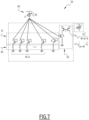
- the VTC 10 comprises a locking frequency generator 12 configured to generate a locking frequency f clk , a current generator 14 configured to generate a biasing current I B , and a relaxation oscillator 18 configured to be powered by the biasing current I B and to generate an output voltage signal V out notably from the locking frequency f clk and the input voltage signal V sig .
- the VTC 10 further comprises a phase difference block 20 configured to determine a phase difference ⁇ between a first signal corresponding to the output voltage signal V out and a second signal corresponding in this embodiment to the locking frequency f clk .
- This phase difference block 20 can be implemented as a simple circuit implementing an XOR logic between two signals.
- the relaxation oscillator 18 is based on a capacitive injection locked oscillator structure, called C-ILO. This structure presents a high swing capability, a good stability against process and temperature variations, and a less area consumption compared to analog implementation. It is explained in further detail in reference to Figure 2 .
- the relaxation oscillator 18 comprises two symmetrical parts 25-1, 25-2 powered by the biasing current I B and an RS latch 26 ("reset-set" latch) connected between the parts 25-1, 25-2.
- Each part 25-1, 25-2 comprises an input inverter block 27 driven by the input voltage signal V sig , a load capacitor C 1 and a switched injection branch 28 with a capacitor block 29 having an injection capacitance C 2 .
- Each inverter block 27 is connected between the corresponding switched injection branch 28 and the load capacitor C 1 on one hand and the RS latch 26 on the other hand.
- each inverter block 27 is at least partially driven the input voltage signal V sig and presents a programmable gain G INV ( m ) based on the gain control word m , as it will be explained below in further detail.
- Each load capacitor C 1 is connected between the corresponding switched injection branch 28 and the inverter block 27.
- the output voltage signal V out is issued from one of the parts 25-1, 25-2 (part 25-1 in the example of Figure 2 ).
- the locking frequency generator 12 is configured to generate the locking frequency f clk so as the steady state phase shift ⁇ 0 of the VTC 10 in the absence of input signal V sig , is equal to ⁇ /2. In this way, the VTC 10 exhibits a fully symmetrical output swing of ⁇ ⁇ /2.
- the relaxation oscillator 18, the current generator 14 and the locking frequency generator 12 can be used to achieve different types of control of the VTC 10.
- four different types of control of the VTC 10 that can be combined between them, can be achieved:
- a linear control of the gain G VTC of the VTC 10 can be achieved by tuning the gain G INV ( m ) of the inverter block 27 comprised in the relaxation oscillator 18, in a linear way.
- G INV m G INV 0 ⁇ m + 1 , where G INV 0 is a reference gain of the inverter block 27.
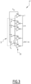
- the inverter block 27 comprises M inverters 30 connected in parallel and first selecting means 31. Among these M inverters 30 one inverter 30 is driven always by the input voltage signal V sig and M-1 inverters 30 can be driven either by the input voltage V sig or a voltage V 0 different from the voltage V sig .
- the voltage V 0 is the voltage of the VTC 10 in absence of the input voltage signal V sig . In other words, V 0 is a polarization voltage of the inverter block 27.
- the selecting means 31 presenting for example a switch for each of M-1 inverters 30 are able to select for each of said inverters 30 the voltage V sig or the voltage V 0 , as it is shown in Figure 3 .
- the first selecting means 31 are controlled so as to drive m inverters 30 under the voltage V sig and M-1-m inverters 30 under the voltage V 0 .
- the capacitor block 29 can consist in only one capacitor having a constant capacitance C 2 .
- the current generator 14 can present any suitable generator providing a constant biasing current I B .
- the locking frequency f clk is unaffected by the control of the inversion gain G INV .
- the locking frequency generator 12 can present a simple clock generator able to provide a constant locking frequency, having for example the optimal value f clk as defined above.
- a dB-linear control of the gain G VTC of the VTC 10 can be achieved by controlling in complementary way the gain G INV ( m ) of the inverter block 27 and the injection capacitance defined by the capacitor block 29.
- the gain G VTC can be controlled based on the gain control word m according to the following expression: G VTC m ⁇ ⁇ C 1 V INV 0 G INV 0 m + K C 2 0 M ⁇ m + K , where:
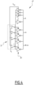
- the inverter block 27 comprises M+K inverters 30 connected in parallel and first selecting means 31.
- K inverters 30 are driven always by the input voltage signal V sig and M inverters 30 can be driven either by the input voltage V sig or the voltage V 0 different from the voltage V sig .
- the selecting means 31 presenting for example a switch for each of M inverters 30 are able to select for each of said inverters 30 the voltage V sig or the voltage V 0 , as it is shown in Figure 4 .
- the first selecting means 31 are controlled so as to drive m inverters 30 under the voltage V sig and M-m inverters 30 under the voltage V 0 .
- G INV 0 G INV max / M + K .
- the capacitor block 29 is tuned in a complementary way to achieve the dB-linear control of the gain G VTC ( m ).
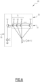
- the capacitor block 29 comprises a plurality of capacitors 40 connected in parallel and second selecting means 42.
- the capacitors 40 one or a plurality of capacitors having their total capacitance equal to G 2 0 K are driven always by the voltage V clk .
- Each of the other capacitors 40 is either connected or disconnected from the circuit by the second selecting means 42 to ensure their total capacitance equal to C 2 0 M ⁇ m .
- the current generator 14 can present any suitable generator providing a constant biasing current I B .
- the injection capacitance C 2 is tuned leading to a variation in the required optimal value of f clk .
- an adaptive locking frequency generator 12 providing a variable locking frequency f clk as function of the injection capacitance C 2 can be used.
- the architecture of the relaxation oscillator 18 is not affected by the linear control of the bandwidth. Thus, any one of the previously described architectures can be used for the relaxation oscillator 18 based on the desired control of the gain.
- the biasing current I B issued from the current generator 14 is controlled in a linear way using the bandwidth control word h .
- the current generator 14 comprises a controlling block 49 ensuring this type control of the biasing current I B ( h ).
- the controlling block 49 comprises a current source 50 providing the reference current IB, a plurality of transistors 51 connected in series to multiply the reference current IB and third selecting means 53 configured to connect/disconnect the transistors 51 so as to deliver the resulting current I B ( h ).
- the required value of f clk is affected through the natural frequency f 0 ⁇ I B .
- an adaptive locking frequency generator 12 providing a variable locking frequency f clk as function of the natural frequency f 0 can be used.
- the locking frequency generator 12 can comprise a free running relaxation oscillator 58 having the same biasing current I B as the relaxation oscillator 18.
- FIG. 8 An example of such a relaxation oscillator 58 is shown in Figure 8 .
- This oscillator is similar to the one shown in Figure 2 but contrary to this last, is provided without the injection branches 28.
- the load capacitors C clk of the relaxation oscillator 58 are adapted to deliver the locking frequency f clk at the output defined by its optimal value as explained above.
- the architecture of the relaxation oscillator 18 is not affected in this case.
- any one of the previously described architectures can be used for the relaxation oscillator 18 based on the desired control of the gain.
- the bandwidth of the VTC 10 is a function of the injection capacitance C 2 .
- an adaptive current bias e.i., I B (1/ m ) is used.
- the current generator 14 further comprises a compensating block 59 connected in the input of the controlling block 49 as previously explained.
- the output of the compensating block 59 is connected as the current source 50 of the controlling block 49.
- the compensating block 59 operates based on the gain control word m, as it shown in Figure 1 .
- the compensating block 59 can be deactivated or the current generator 14 can be provided without this compensating block 59.
- the compensating block 59 comprises a current source 60 providing the reference current IB, a plurality of transistors 61 connected to the current source 60 in a parallel way between them, fourth selecting means 64 configured to connect/disconnect the transistors and an output branch 65.
- a unique transistor of size K can be used instead of K permanently connected transistors.
- the injection capacitance C 2 is tuned leading to a variation in the required optimal value of f clk .
- an adaptive locking frequency generator 12 providing a variable locking frequency f clk as function of the injection capacitance C 2 and the biasing current I B can be used.
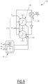
- a VTC 110 according to a second embodiment is schematically shown in Figure 9 .
- the VTC 110 according to this embodiment is similar to the one of the first embodiment, explained in reference to Figure 1 .
- this VTC 110 comprises a current generator 14, a relaxation oscillator 18 and a phase difference block 20 which are similar to those explained above and will not be explained in reference to this embodiment.
- the VTC 110 also comprises a locking frequency generator 112 having a structure different from the one explained above.
- the locking frequency generator 112 is formed by a pair of self-locked-injection oscillators.
- One of these oscillators is the relaxation oscillator 18 as previously explained.
- the other oscillator, denoted in Figure 9 by reference 119, is similar to the relaxation oscillator 18. However, the output of this oscillator 119 is connected to the input of the oscillator 18 and the output of the oscillator 18 is connected to the input of the oscillator 119.
- the locking frequency generator 112 is particularly advantageous when an accurate control of the locking frequency f clk is needed and/or its control is not simple. This is especially the case of dB-linear control of the gain. It should be noted that according to this embodiment, no adaptive clock is necessary since the system formed by the oscillators 18, 119 is auto-oscillating.
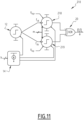
- a VTC 210 according to a third embodiment is schematically shown in Figure 11 .
- the VTC 210 according to this embodiment is similar to the VTC 10 according to the first embodiment, explained in reference to Figure 1 .
- this VTC 210 comprises a current generator 14, a locking frequency generator 12 and a phase difference block 20 which are similar to those explained above and will not be explained in reference to this embodiment.
- the input voltage signal V sig of the VTC 210 presents a differential signal defining a component V sig + and a component V sig - .
- the VTC 210 comprises a relaxation oscillator 218, 219 for each component of the differential signal V sig .
- the relaxation oscillators 218, 219 are connected in parallel between the locking frequency generator 12 and the phase difference block 20.
- each relaxation oscillator 218, 219 is similar to the relaxation oscillator 18 explained in reference to the first embodiment and is configured to output an output voltage signal from the corresponding component of the differential input signal V sig and the same locking frequency f clk provided by the locking frequency generator 12.
- the phase difference block 20 is configured to determine a phase difference ⁇ between a first signal corresponding to the output voltage signal from the relaxation oscillator 218 and a second signal corresponding in this embodiment to the output voltage signal from the relaxation oscillator 219. As shown in Figure 11 , the phase difference block 20 is configured to apply the XOR logic between the received signals.
- the application of the XOR logic in this case is equivalent to a sum of two phases, each phase corresponding to the result of subtraction for each relaxation oscillator between its output voltage signal and the locking frequency f clk .
- the application of the XOR logic comprises a determination of a phase based on the difference between the output voltage signal from at least one relaxation oscillator and the locking frequency f clk .
- the locking frequency generator 12 can be realized according to any one of the preceding examples.
- the locking frequency generator 12 presents a free running relaxation oscillator similar to the one explained in reference to Figure 8 .
- the VTC 210 is particularly suitable for a linear control of gain and/or bandwidth.
- a VTC 310 according to a fourth embodiment is schematically shown in Figure 12 .
- the VTC 310 according to this embodiment is similar to the VTC 110 according to the second embodiment (explained in reference to Figure 9 ) but is adapted to operate with a differential input signal V sig as explained in reference to the previous embodiment.
- this VTC 310 comprises a locking frequency generator 312 which is formed by a pair of self-locked-injection oscillators 318, 319.
- These oscillators 318, 319 are similar to the oscillators 218, 219 explained in relation with the previous embodiment.
- each of these oscillators 318, 319 is run under the respective component V sig + , V sig - of the differential input signal.
- the output of the oscillator 319 providing the locking frequency f clk as explained above is connected to the input of the oscillator 318 and to the phase difference block 20.
- the output of the oscillator 318 is connected to the input of the oscillator 319 and to the phase difference block 20.
- the phase difference block 20 is configured to determine a phase difference ⁇ between a first signal corresponding to the output voltage signal from the relaxation oscillator 318 and a second signal corresponding to the locking frequency f clk issued from the relaxation oscillator 319. As shown in Figure 11 , the phase difference block 20 is configured to apply the XOR logic between the received signals.
- the VTC 310 can be used to control the bandwidth in a linear way and the gain in a linear or a dB-linear way.
- VTC voltage-to-Velator
- the structure of a VTC according to a fifth embodiment can be similar to any one explained in reference with the previous embodiments.
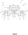
- the only difference of the VTC according to this embodiment is the structure of a relaxation oscillator 418 which will be explained in further detail below in reference to Figure 13 .
- the relaxation oscillator 418 is based on a capacitive injection locked oscillator structure, called C-ILO. Additionally, like in the previous embodiments, the oscillator 418 comprises two symmetrical parts 425-1 , 425-2 powered by the biasing current I B and an RS latch 26 ("reset-set" latch) connected between the parts 425-1, 425-2. Also like in the previous cases, each part 425-1, 425-2 comprises a switched injection branch 28 comprising a capacitor block 29 having an injection capacitance C 2 which may be eventually controlled using the gain control word m as previously explained.
- C-ILO capacitive injection locked oscillator structure
- each part 425-1 , 425-2 of the relaxation oscillator 418 comprises a comparator 426 connected to the input voltage signal V sig via a DC-decoupling unity.
- the reference inversion level V INV 0 here can be directly set by decoupling the input of the comparator 426 from the signal of interest. This decoupling also helps in reducing the input offset.
- the inversion gain G INV as previously explained is substantially equal to 1 and the gain of the whole VTC can be found using the following expression: G VTC m ⁇ ⁇ V INV 0 C 1 C 2 .
- linear gain control can be performed by tuning the capacitance C 1
- dB-linear gain control can be achieved by tinning both C 1 and C 2 in a complementary way.
- each part 425-1, 425-2 of the relaxation oscillator 418 comprises a load capacitor block 427 presenting a linearly controllable capacitance C 1 based on the gain control word m .
- This control can be carried out using a structure similar to the one shown and explained with reference to Figure 5 .
- the load capacitor block 427 can have a plurality of capacitors configured to be connected in parallel by selecting means in order to control linearly the resulting capacitance.
Landscapes
- Engineering & Computer Science (AREA)
- Theoretical Computer Science (AREA)
- Stabilization Of Oscillater, Synchronisation, Frequency Synthesizers (AREA)
Abstract
The invention concerns a programmable voltage to time converter (10), comprising:
- a locking frequency generator (12) configured to generate a locking frequency;
- a current generator (14) configured to generate a biasing current;
- a relaxation oscillator (18) configured to be powered by the biasing current and to generate an output voltage signal from the locking frequency, a gain control word and an input voltage signal;
- a phase difference block (20) configured to determine a phase difference between a first signal corresponding to the output voltage signal and a second signal determined based on the locking frequency.
- a locking frequency generator (12) configured to generate a locking frequency;
- a current generator (14) configured to generate a biasing current;
- a relaxation oscillator (18) configured to be powered by the biasing current and to generate an output voltage signal from the locking frequency, a gain control word and an input voltage signal;
- a phase difference block (20) configured to determine a phase difference between a first signal corresponding to the output voltage signal and a second signal determined based on the locking frequency.
The relaxation oscillator (18) comprises a component presenting a linearly controllable characteristic. The voltage to time converter (10) presents a gain linearly or dB-linearly controllable based on the gain control word by controlling linearly said characteristic of said component.
Description
- The invention concerns a programmable voltage to time converter, also called VTC. The voltage to time converter according to the invention has a programmable gain and/or signal bandwidth.
- The current trend in smart portable and battery-powered devices requires sensors with many low power integrate circuits such as, amplifier, analog to digital converter (ADC), and classifier to provide intelligent data collection. Designers look to a digital-oriented design of these systems to accommodate the trends of technology scaling, and lower supply voltage for power reduction.
- For these reasons, high efficient analog to information architectures start to process the signal in the time domain by duty cycling the analog quantity using voltage-to-time converter block (VTC). This time-encoded signal is not limited by voltage headroom, and is considerably more robust than the analog signal when experiencing process, supply and temperature variations. It also benefit from higher frequency resolution considering technology scaling.
- However, high efficient conversion need a real time signal conditioning to process a wide range of signal strength. However, VTC architectures have a low conversion gain and are usually preceded by a preamplifier stage or automatic gain control for signal conditioning.
- Thus, there is an interest in providing a voltage to time converter (VTC) with a tunable gain.
- In the art, the existing VTC topologies are mainly composed into two categories: variable slope (VS) VTC, and constant-slope (CS) VTC.
- As for the variable slope VTC, some architectures of this type can provide a gain control but with only one degree of freedom that could be used. In other architectures of this type, the gain can be more easily tuned through the injection current. However, the output swing of this architecture is highly distorted around the limits [0, π].
- As for the constant-slope VTC, like in the previous case, some architectures of this type can provide only one degree of freedom for the gain control which can be difficultly tuned. Some other architectures provide more degrees of freedom for the gain control but their tuning can be difficultly carried out in practice.
- An aim of the present invention is to provide a programmable voltage to time converter with a tunable gain, which is able to overcome the above-mentioned drawbacks of the art.
- For this purpose, the inventions relates to a programmable voltage to time converter, comprising a locking frequency generator configured to generate a locking frequency, a current generator configured to generate a biasing current, a relaxation oscillator configured to be powered by the biasing current and to generate an output voltage signal from the locking frequency, a gain control word and an input voltage signal, a phase difference block configured to determine a phase difference between a first signal corresponding to the output voltage signal and a second signal determined based on the locking frequency, the relaxation oscillator comprising a component presenting a linearly controllable characteristic and the voltage to time converter presenting a gain linearly or dB-linearly controllable based on the gain control word by controlling linearly said characteristic of said component.
- Alternatively, the programmable voltage to time converter comprises a phase difference block configured to determine at least one phase based on the difference between the output voltage signal issued from the relaxation oscillator and the locking frequency.
- Provided with these features, the invention ensures an accurate and easy gain control of the voltage to time converter, without a preamplifier stage (comprising for example an LNA "Low Noise Amplifier") or automatic gain control for signal conditioning. Thus, the VTC according to the invention is more compact and deprived of inconveniences of the preamplifier stage or other additional components. This is achieved using a relaxation oscillator having a capacitive injection locked oscillator structure, called C-ILO. This relaxation oscillator is provided with a component presenting a linearly controllable characteristic. Thus, the gain of the whole system can be finely controlled by controlling this characteristic with tunable range and step size. The range and the step can be easily adapted to each application.
- Compared with the conventional architecture, the VTC according to the invention can amplify and convert the input voltage in a one-step leading to a reduced complexity, and power consumption.
- The present invention can accurately operate using a supply voltage of only several hundred millivolts while maintaining a low distortion and rail-to-rail conversion. Additionally, it is compatible with single or differential input.
- The proposed VTC can be interfaced with all types of sensors, especially analog to information architecture that usually require a large SNR ("Signal-to-Noise Ratio") for better efficiency. It can advantageously be used for low power applications such as biomedical, loT ("Internet of Things"), wake up sensors, and low power and low distortion time based ADC.
- Additionally, the invention eliminates the need of large passive components (such as capacitances for example) for low pass filtering since the bandwidth is a function of the ratio of the load and injection capacities. This ratio can be chosen accordingly.
- According to some embodiments, said component is an input inverter block driven at least partially by the input voltage signal and connected to an output of the relaxation oscillator; the input inverter block presenting a gain linearly controllable based on the gain control word; said characteristic corresponding to the gain of the input inverter block.
- According to some embodiments, the input inverter block comprises M inverters connected in parallel and first selecting means configured to control the gain of the input inverter block by selecting among these M inverters m inventers to be driven by the input voltage signal and at least M-m-1 inverters to be driven by a voltage signal different from the input voltage signal, the number m being defined based on the gain control word.
- According to some embodiments, the input inverter block further comprises K additional inverters configured to be driven by the input voltage signal, K being a constant factor; the first selecting means being configured to control the gain of the input inverter block by selecting among M+K inverters m inventers to be driven by the input voltage signal and M-m inverters to be driven by said voltage signal different from the input voltage signal.
- According to some embodiments, said component is a load capacitor block a capacitance linearly controllable based on the gain control word; said characteristic corresponding to the capacitance of the load capacitor block.
- According to some embodiments, the relaxation oscillator further comprises a switched injection branch configured to inject a voltage defined by the locking frequency and comprising a capacitor block defining an injection capacitance.
- According to some embodiments, the injection capacitance is chosen constant for a linear control of the gain of the voltage to time converter.
- According to some embodiments, the capacitor block comprises second selecting means configured to control the injection capacitance in a complementary way to said characteristic of said component, for a dB-linear control of the gain of the voltage to time converter.
- According to some embodiments, the second selecting means are configured to control the injection capacitance in a linear way, based on the gain control word.
- According to some embodiments, the current generator is configured to generate the biasing current based on a bandwidth control word, for a linear control of the bandwidth of the voltage to time converter.
- According to some embodiments, the current generator comprises a controlling block configured to linearly control the biasing current based on the bandwidth control word.
- According to some embodiments, the current generator further comprises a compensating block connected to an input of the controlling block and configured to generate, based on the gain control word, a current compensating variations of the injection capacitance.
- According to some embodiments, the locking frequency generator is formed by one of the following elements:
- a regular clock to provide a constant locking frequency;
- an adaptive clock to provide an adaptive locking frequency;
- a free running relaxation oscillator powered by the biasing current and comprising a load capacitor defining a capacitance adapted to provide an adaptive locking frequency.
- According to some embodiments, the locking frequency generator is formed by the relaxation oscillator and an additional relaxation oscillator connected to said relaxation oscillator to form an auto-oscillating system.
- According to some embodiments, the input voltage signal is a differential voltage signal having two components, the programmable voltage to time converter comprising a relaxation oscillator for each component of the input voltage signal.
- According to some embodiments, the first and second signals for the phase difference block correspond to output voltage signals issued from different relaxation oscillators.
- According to some embodiments, the second signal for the phase difference block is provided by the locking frequency.
- The invention and its advantages will be better understood upon reading the following description, which is given solely by way of non-limiting example and which is made with reference to the appended drawings, in which:
- [
Fig 1] Figure 1 is a schematic view of a voltage to time converter according to a first embodiment of the invention; - [
Fig 2 ] [Fig 3 ] [Fig 4 ] [Fig 5 ] [Fig 6 ] [Fig 7 ] [Fig 8 ]Figures 2 to 8 show particular examples of implementation of different components of the voltage to time converter ofFigure 1 ; - [
Fig 9] Figure 9 is a schematic view of a voltage to time converter according to a second embodiment of the invention; - [
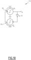
Fig 10] Figure 10 shows the operation of a component of the voltage to time converter ofFigure 9 ; - [
Fig 11] Figure 11 is a schematic view of a voltage to time converter according to third embodiment of the invention; - [
Fig 12] Figure 12 is a schematic view of a voltage to time converter according to a fourth embodiment of the invention; and - [
Fig 13] Figure 13 is a schematic view of a component of a voltage to time converter according to a fifth embodiment of the invention. -
Figure 1 shows a programmable voltage totime converter 10, also calledVTC 10, according to a first embodiment of the invention. - The
VTC 10 is for example usable in an analog to digital converter (ADC) and is able to provide a phase or delay or time value from an input voltage signal. The input voltage signal corresponds for example to a measuring signal. Thus, for example, theVTC 10 can be used as a component of a sensor system providing digital values of a measured physical parameter. TheVTC 10 provides a phase gain normalized by a probe frequency deg/V. - The
VTC 10 presents a tunable gain and signal bandwidth in respect with the given gain. The gain control is carried out using a gain control word m and the bandwidth control is carried out using a bandwidth control word h. In other words, m and h present control commands usable to tune respectfully the gain and the signal bandwidth of theVTC 10. As it will be apparent in the further description, the gain control and the signal bandwidth control of theVTC 10 are independent one from the other. - Additionally, the
VTC 10 can be controlled in a linear way for moderate input signal swing (for example less than 10 dB) and in a linear in decibel way (so called dB-linear way) for wide input signal swing (for example greater than 20 dB). Each type of these controls will be explained in further detail below. - As it is shown in
Figure 1 , theVTC 10 comprises alocking frequency generator 12 configured to generate a locking frequency fclk , acurrent generator 14 configured to generate a biasing current IB , and arelaxation oscillator 18 configured to be powered by the biasing current IB and to generate an output voltage signal Vout notably from the locking frequency fclk and the input voltage signal Vsig . - The
VTC 10 further comprises aphase difference block 20 configured to determine a phase difference φ between a first signal corresponding to the output voltage signal Vout and a second signal corresponding in this embodiment to the locking frequency fclk. Thisphase difference block 20 can be implemented as a simple circuit implementing an XOR logic between two signals. - The
relaxation oscillator 18 is based on a capacitive injection locked oscillator structure, called C-ILO. This structure presents a high swing capability, a good stability against process and temperature variations, and a less area consumption compared to analog implementation. It is explained in further detail in reference toFigure 2 . - Thus, as it is shown in
Figure 2 , therelaxation oscillator 18 comprises two symmetrical parts 25-1, 25-2 powered by the biasing current IB and an RS latch 26 ("reset-set" latch) connected between the parts 25-1, 25-2. Each part 25-1, 25-2 comprises aninput inverter block 27 driven by the input voltage signal Vsig , a load capacitor C 1 and a switchedinjection branch 28 with acapacitor block 29 having an injection capacitance C 2. Eachinverter block 27 is connected between the corresponding switchedinjection branch 28 and the load capacitor C 1 on one hand and theRS latch 26 on the other hand. Additionally, eachinverter block 27 is at least partially driven the input voltage signal Vsig and presents a programmable gain GINV (m) based on the gain control word m, as it will be explained below in further detail. Each load capacitor C 1 is connected between the corresponding switchedinjection branch 28 and theinverter block 27. The output voltage signal Vout is issued from one of the parts 25-1, 25-2 (part 25-1 in the example ofFigure 2 ). - The
locking frequency generator 12 is configured to generate the locking frequency fclk so as the steady state phase shift φ 0 of theVTC 10 in the absence of input signal Vsig , is equal to π/2. In this way, theVTC 10 exhibits a fully symmetrical output swing of ± π/2. In fact, the output swing in term of the modulated natural frequency f 0(Vsig ) is given by:

whole VTC 10, i.e. frequency in absence of the input voltage signal Vsig . - Advantageously, an optimal value of the locking frequency fclk when φ 0 = π/2 so it can be given determined by the following expression:

- Different examples of implementation of the
relaxation oscillator 18, thecurrent generator 14 and thelocking frequency generator 12 can be used to achieve different types of control of theVTC 10. Particularly, four different types of control of theVTC 10 that can be combined between them, can be achieved: - linear control of the gain;
- dB-linear control of the gain;
- linear control of the bandwidth with a linear control of the gain; and
- linear control of the bandwidth with a dB-linear control of the gain.
- An example of implementation for each of the types of each of the
relaxation oscillator 18, thecurrent generator 14 andlocking frequency generator 12 will be given below. - According to the invention, a linear control of the gain GVTC of the
VTC 10 can be achieved by tuning the gain GINV (m) of theinverter block 27 comprised in therelaxation oscillator 18, in a linear way. Particularly, the following expression can be used to control the gain GINV (m) of the inverter block 27:

inverter block 27. - A possible embodiment of the
inverter block 27 with a tunable gain GINV (m) for the purpose of linear control is shown inFigure 3 . According to this Figure, theinverter block 27 comprises Minverters 30 connected in parallel and first selectingmeans 31. Among theseM inverters 30 oneinverter 30 is driven always by the input voltage signal Vsig and M-1inverters 30 can be driven either by the input voltage Vsig or a voltage V 0 different from the voltage Vsig . The voltage V 0 is the voltage of theVTC 10 in absence of the input voltage signal Vsig . In other words, V 0 is a polarization voltage of theinverter block 27. - Particularly, the selecting means 31 presenting for example a switch for each of M-1
inverters 30 are able to select for each of saidinverters 30 the voltage Vsig or the voltage V 0, as it is shown inFigure 3 . - Assuming that all of the
inventers 30 are substantially identical and denoting as
inverter block 27 is able to provide, the gain GINV (m) can be tuned based on the gain control word m in the following way:
- For achieving this expression, the first selecting
means 31 are controlled so as to drive minverters 30 under the voltage Vsig and M-1-m inverters 30 under the voltage V 0. - The reference
gain 

- In this example, the
capacitor block 29 can consist in only one capacitor having a constant capacitance C 2. - According to this type of control, the
current generator 14 can present any suitable generator providing a constant biasing current IB. - Additionally, according to this type of control, the locking frequency fclk is unaffected by the control of the inversion gain GINV. Thus, the
locking frequency generator 12 can present a simple clock generator able to provide a constant locking frequency, having for example the optimal value fclk as defined above. - According to the invention, a dB-linear control of the gain GVTC of the
VTC 10 can be achieved by controlling in complementary way the gain GINV (m) of theinverter block 27 and the injection capacitance defined by thecapacitor block 29. Particularly, in this case, the gain GVTC can be controlled based on the gain control word m according to the following expression:
-

inverter block 27; -

inverter block 27 at the input common mode voltage V 0; -

capacitor block 29; - K is a constant factor responsible in defining the tuning range and the control step.
- In other words, as in the previous case, the inventor gain GINV of the
inverter block 27 can be still controlled in a linear way but using the factor m + K instead of m + 1, i.e. GINV (m) = (m + K). - A possible embodiment of the
inverter block 27 with a tunable gain GINV (m) for the purpose of dB-linear control is shown inFigure 4 . According to this Figure, theinverter block 27 comprises M+K inverters 30 connected in parallel and first selectingmeans 31. Among these M+K inverters 30, Kinverters 30 are driven always by the input voltage signal Vsig andM inverters 30 can be driven either by the input voltage Vsig or the voltage V 0 different from the voltage Vsig . Particularly, the selecting means 31 presenting for example a switch for each ofM inverters 30 are able to select for each of saidinverters 30 the voltage Vsig or the voltage V 0, as it is shown inFigure 4 . - Assuming that all of the
inventers 30 are substantially identical and denoting as
block 27 is able to provide, the gain GINV (m) can be tuned based on the gain control word m in the following way:
- For achieving this expression, the first selecting
means 31 are controlled so as to drive minverters 30 under the voltage Vsig andM-m inverters 30 under the voltage V 0. - Contrary to the previous case, in this example, the reference
gain 

- As mentioned above, the
capacitor block 29 is tuned in a complementary way to achieve the dB-linear control of the gain GVTC (m). In other words, the capacitance C 2 is controlled linearly according to the following expression:
- For this purpose, a possible embodiment of the
capacitor block 29 is shown inFigure 5 . According to this embodiment, thecapacitor block 29 comprises a plurality ofcapacitors 40 connected in parallel and second selectingmeans 42. Among thecapacitors 40, one or a plurality of capacitors having their total capacitance equal to
other capacitors 40 is either connected or disconnected from the circuit by the second selecting means 42 to ensure their total capacitance equal to
- According to this type of control, the
current generator 14 can present any suitable generator providing a constant biasing current IB. - In the case of dB-linear gain control, the injection capacitance C 2 is tuned leading to a variation in the required optimal value of fclk. In this case, an adaptive
locking frequency generator 12 providing a variable locking frequency fclk as function of the injection capacitance C 2 can be used. - The architecture of the
relaxation oscillator 18 is not affected by the linear control of the bandwidth. Thus, any one of the previously described architectures can be used for therelaxation oscillator 18 based on the desired control of the gain. - For linear control of the bandwidth, the biasing current IB issued from the
current generator 14 is controlled in a linear way using the bandwidth control word h. Particularly, in this case, the bandwidth fBW of theVTC 10 is expressed in the following way: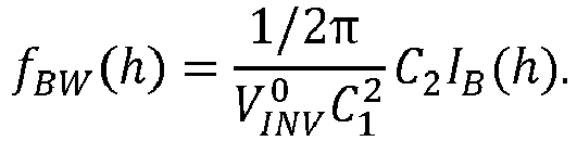
- Assuming that the basing current IB is linearly controlled so as:

current generator 14 comprises a controllingblock 49 ensuring this type control of the biasing current IB (h). - A possible embodiment of the controlling
block 49 is shown inFigure 6 . According to this embodiment, the controllingblock 49 comprises acurrent source 50 providing the reference current IB, a plurality oftransistors 51 connected in series to multiply the reference current IB and third selecting means 53 configured to connect/disconnect thetransistors 51 so as to deliver the resulting current IB (h). For this purpose, the third selectingmeans 53 may comprise a switch associated to eachtransistor 51. To achieve the resulting current
means 53 are able to connect to the circuit h + 1transistors 51. - In the case of linear bandwidth control through the biasing current IB , the required value of fclk is affected through the natural frequency f 0 ∝ IB. In this case, an adaptive
locking frequency generator 12 providing a variable locking frequency fclk as function of the natural frequency f 0 can be used. Alternatively, thelocking frequency generator 12 can comprise a freerunning relaxation oscillator 58 having the same biasing current IB as therelaxation oscillator 18. - An example of such a
relaxation oscillator 58 is shown inFigure 8 . This oscillator is similar to the one shown inFigure 2 but contrary to this last, is provided without theinjection branches 28. Additionally, the load capacitors Cclk of therelaxation oscillator 58 are adapted to deliver the locking frequency fclk at the output defined by its optimal value as explained above. For this purpose, the capacitance of each load capacitor Cclk can be defined as follows:
- The architecture of the
relaxation oscillator 18 is not affected in this case. Thus, any one of the previously described architectures can be used for therelaxation oscillator 18 based on the desired control of the gain. - As seen above, the bandwidth of the
VTC 10 is a function of the injection capacitance C 2. Thus, its value is subject to change when the gain is tuned through C 2(m ) wherem = M - m + K. To compensate this variation an adaptive current bias, e.i., IB (1/m ), is used. - For this purpose, in case of a linear control of the bandwidth with a dB-linear control of the gain, the
current generator 14 further comprises a compensatingblock 59 connected in the input of the controllingblock 49 as previously explained. In other words, in the example ofFigure 6 , the output of the compensatingblock 59 is connected as thecurrent source 50 of the controllingblock 49. The compensatingblock 59 operates based on the gain control word m, as it shown inFigure 1 . In case of a linear-control of the bandwidth for a linear control of the gain, the compensatingblock 59 can be deactivated or thecurrent generator 14 can be provided without this compensatingblock 59. - A possible embodiment of the compensating
block 59 is shown inFigure 7 . According to this embodiment, the compensatingblock 59 comprises acurrent source 60 providing the reference current IB, a plurality oftransistors 61 connected to thecurrent source 60 in a parallel way between them, fourth selecting means 64 configured to connect/disconnect the transistors and anoutput branch 65. Among the transistors, K transistors are connected permanently to the circuit and the fourth selectingmeans 64 are able to connect M-m transistors, to divide the referencecurrent 
m = M - m + K. Theoutput branch 65 further comprises K permanently connected transistors to multiply the divided current by K, as the resulting current is defined according to the following expressions:
- In a variant, instead of K permanently connected transistors, a unique transistor of size K can be used. In this case, the current needed to maintain the required bandwidth at the maximum gain (m=M) is equal to IB which can be easily set by the designer.
- As in the case of dB-linear gain control, in the present example, the injection capacitance C 2 is tuned leading to a variation in the required optimal value of fclk. In this case, an adaptive
locking frequency generator 12 providing a variable locking frequency fclk as function of the injection capacitance C 2 and the biasing current IB can be used. - A
VTC 110 according to a second embodiment is schematically shown inFigure 9 . TheVTC 110 according to this embodiment is similar to the one of the first embodiment, explained in reference toFigure 1 . Particularly, thisVTC 110 comprises acurrent generator 14, arelaxation oscillator 18 and aphase difference block 20 which are similar to those explained above and will not be explained in reference to this embodiment. - The
VTC 110 according to the second embodiment also comprises alocking frequency generator 112 having a structure different from the one explained above. - Particularly, according to this embodiment, the
locking frequency generator 112 is formed by a pair of self-locked-injection oscillators. One of these oscillators is therelaxation oscillator 18 as previously explained. The other oscillator, denoted inFigure 9 byreference 119, is similar to therelaxation oscillator 18. However, the output of thisoscillator 119 is connected to the input of theoscillator 18 and the output of theoscillator 18 is connected to the input of theoscillator 119. - Assuming, that both
oscillators oscillators Figure 10 . - The
locking frequency generator 112 is particularly advantageous when an accurate control of the locking frequency fclk is needed and/or its control is not simple. This is especially the case of dB-linear control of the gain. It should be noted that according to this embodiment, no adaptive clock is necessary since the system formed by theoscillators - A
VTC 210 according to a third embodiment is schematically shown inFigure 11 . TheVTC 210 according to this embodiment is similar to theVTC 10 according to the first embodiment, explained in reference toFigure 1 . Particularly, thisVTC 210 comprises acurrent generator 14, alocking frequency generator 12 and aphase difference block 20 which are similar to those explained above and will not be explained in reference to this embodiment. - Contrary to the first embodiment, the input voltage signal Vsig of the
VTC 210 according to the third embodiment presents a differential signal defining a component V sig+ and a component V sig-. In this embodiment, theVTC 210 comprises arelaxation oscillator Figure 11 , therelaxation oscillators locking frequency generator 12 and thephase difference block 20. - Particularly, each
relaxation oscillator relaxation oscillator 18 explained in reference to the first embodiment and is configured to output an output voltage signal from the corresponding component of the differential input signal Vsig and the same locking frequency fclk provided by thelocking frequency generator 12. Thephase difference block 20 is configured to determine a phase difference φ between a first signal corresponding to the output voltage signal from therelaxation oscillator 218 and a second signal corresponding in this embodiment to the output voltage signal from therelaxation oscillator 219. As shown inFigure 11 , thephase difference block 20 is configured to apply the XOR logic between the received signals. The application of the XOR logic in this case is equivalent to a sum of two phases, each phase corresponding to the result of subtraction for each relaxation oscillator between its output voltage signal and the locking frequency fclk. In other words, the application of the XOR logic comprises a determination of a phase based on the difference between the output voltage signal from at least one relaxation oscillator and the locking frequency fclk. - The
locking frequency generator 12 can be realized according to any one of the preceding examples. In the example ofFigure 11 , thelocking frequency generator 12 presents a free running relaxation oscillator similar to the one explained in reference toFigure 8 . Thus, in this example, theVTC 210 is particularly suitable for a linear control of gain and/or bandwidth. - A
VTC 310 according to a fourth embodiment is schematically shown inFigure 12 . TheVTC 310 according to this embodiment is similar to theVTC 110 according to the second embodiment (explained in reference toFigure 9 ) but is adapted to operate with a differential input signal Vsig as explained in reference to the previous embodiment. - Particularly, this
VTC 310 comprises alocking frequency generator 312 which is formed by a pair of self-locked-injection oscillators oscillators oscillators oscillators oscillator 319 providing the locking frequency fclk as explained above is connected to the input of theoscillator 318 and to thephase difference block 20. The output of theoscillator 318 is connected to the input of theoscillator 319 and to thephase difference block 20. Thephase difference block 20 is configured to determine a phase difference φ between a first signal corresponding to the output voltage signal from therelaxation oscillator 318 and a second signal corresponding to the locking frequency fclk issued from therelaxation oscillator 319. As shown inFigure 11 , thephase difference block 20 is configured to apply the XOR logic between the received signals. - According to this embodiment, the
VTC 310 can be used to control the bandwidth in a linear way and the gain in a linear or a dB-linear way. - The structure of a VTC according to a fifth embodiment can be similar to any one explained in reference with the previous embodiments. The only difference of the VTC according to this embodiment is the structure of a
relaxation oscillator 418 which will be explained in further detail below in reference toFigure 13 . - As in the previous embodiments, the
relaxation oscillator 418 is based on a capacitive injection locked oscillator structure, called C-ILO. Additionally, like in the previous embodiments, theoscillator 418 comprises two symmetrical parts 425-1 , 425-2 powered by the biasing current IB and an RS latch 26 ("reset-set" latch) connected between the parts 425-1, 425-2. Also like in the previous cases, each part 425-1, 425-2 comprises a switchedinjection branch 28 comprising acapacitor block 29 having an injection capacitance C 2 which may be eventually controlled using the gain control word m as previously explained. - Contrary to the previously explained examples, instead of an input inverter block, each part 425-1 , 425-2 of the
relaxation oscillator 418 comprises acomparator 426 connected to the input voltage signal Vsig via a DC-decoupling unity. The reference inversionlevel 
comparator 426 from the signal of interest. This decoupling also helps in reducing the input offset. - In this case, the inversion gain GINV as previously explained is substantially equal to 1 and the gain of the whole VTC can be found using the following expression:

- Thus, linear gain control can be performed by tuning the capacitance C 1, while dB-linear gain control can be achieved by tinning both C 1 and C 2 in a complementary way.
- For this purpose, instead of a simple load capacitor C 1 as previously explained, each part 425-1, 425-2 of the
relaxation oscillator 418 comprises aload capacitor block 427 presenting a linearly controllable capacitance C 1 based on the gain control word m. This control can be carried out using a structure similar to the one shown and explained with reference toFigure 5 . Particularly, as in the case ofFigure 5 , theload capacitor block 427 can have a plurality of capacitors configured to be connected in parallel by selecting means in order to control linearly the resulting capacitance.
Claims (17)
- A programmable voltage to time converter (10; 110; 210; 310), comprising:- a locking frequency generator (12; 112; 312) configured to generate a locking frequency;- a current generator (14) configured to generate a biasing current;- a relaxation oscillator (18; 218; 318; 418) configured to be powered by the biasing current and to generate an output voltage signal from the locking frequency, a gain control word and an input voltage signal;- a phase difference block (20) configured to determine a phase difference between a first signal corresponding to the output voltage signal and a second signal determined based on the locking frequency;the relaxation oscillator (18; 218; 318; 418) comprising a component (27; 427) presenting a linearly controllable characteristic;the voltage to time converter (10; 110; 210; 310) presenting a gain linearly or dB-linearly controllable based on the gain control word by controlling linearly said characteristic of said component (27; 427).
- The programmable voltage to time converter (10; 110; 210; 310) according to claim 1, wherein said component is an input inverter block (27) driven at least partially by the input voltage signal and connected to an output of the relaxation oscillator (18; 218; 318);the input inverter block (27) presenting a gain linearly controllable based on the gain control word;said characteristic corresponding to the gain of the input inverter block (27).
- The programmable voltage to time converter (10; 110; 210; 310) according to claim 2, wherein the input inverter block (27) comprises M inverters (30) connected in parallel and first selecting means (31) configured to control the gain of the input inverter block (27) by selecting among these M inverters (30) m inventers (30) to be driven by the input voltage signal and at least M-m-1 inverters (30) to be driven by a voltage signal different from the input voltage signal, the number m being defined based on the gain control word.
- The programmable voltage to time converter (10; 110; 210; 310) according to claim 3, wherein the input inverter block (27) further comprises K additional inverters (30) configured to be driven by the input voltage signal, K being a constant factor;
the first selecting means (31) being configured to control the gain of the input inverter block (27) by selecting among M+K inverters (30) m inventers (30) to be driven by the input voltage signal and M-m inverters (30) to be driven by said voltage signal different from the input voltage signal. - The programmable voltage to time converter (10; 110; 210; 310) according to claim 1, wherein said component is a load capacitor block (427) presenting a capacitance linearly controllable based on the gain control word;
said characteristic corresponding to the capacitance of the load capacitor block (427). - The programmable voltage to time converter (10; 110; 210; 310) according to any one of the preceding claims, wherein the relaxation oscillator (18; 218; 318; 418) further comprises a switched injection branch (28) configured to inject a voltage defined by the locking frequency and comprising a capacitor block (29) defining an injection capacitance.
- The programmable voltage to time converter (10; 110; 210; 310) according to claim 6, wherein the injection capacitance is chosen constant for a linear control of the gain of the voltage to time converter (10; 110; 210; 310).
- The programmable voltage to time converter (10; 110; 210; 310) according to claim 6, wherein the capacitor block (29) comprises second selecting means (42) configured to control the injection capacitance in a complementary way to said characteristic of said component (27; 427), for a dB-linear control of the gain of the voltage to time converter (10; 110; 210; 310).
- The programmable voltage to time converter (10; 110; 210; 310) according to claim 8, wherein the second selecting means (42) are configured to control the injection capacitance in a linear way, based on the gain control word.
- The programmable voltage to time converter (10; 110; 210; 310) according to any one of the preceding claims, wherein the current generator (14) is configured to generate the biasing current based on a bandwidth control word, for a linear control of the bandwidth of the voltage to time converter (10; 110; 210; 310).
- The programmable voltage to time converter (10; 110; 210; 310) according to claim 10, wherein the current generator (14) comprises a controlling block (49) configured to linearly control the biasing current based on the bandwidth control word.
- The programmable voltage to time converter (10; 110; 210; 310) according to claim 11 taken in combination with claim 8 or 9, wherein the current generator (14) further comprises a compensating block (59) connected to an input of the controlling block (49) and configured to generate, based on the gain control word, a current compensating variations of the injection capacitance.
- The programmable voltage to time converter (10; 210) according to any one of the preceding claims, wherein the locking frequency generator (12) is formed by one of the following elements:- a regular clock to provide a constant locking frequency;- an adaptive clock to provide an adaptive locking frequency;- a free running relaxation oscillator (58) powered by the biasing current and comprising a load capacitor defining a capacitance adapted to provide an adaptive locking frequency.
- The programmable voltage to time converter (110; 310) according to any one of claims 1 to 12, wherein the locking frequency generator (12) is formed by the relaxation oscillator (18; 318; 418) and an additional relaxation oscillator (119; 319) connected to said relaxation oscillator (18; 318; 418) to form an auto-oscillating system.
- The programmable voltage to time converter (210; 310) according to any one of the preceding claims, wherein the input voltage signal is a differential voltage signal having two components;
the programmable voltage to time converter (210; 310) comprising a relaxation oscillator (218, 219; 318, 319) for each component of the input voltage signal. - The programmable voltage to time converter (210) according to claim 15, wherein the first and second signals for the phase difference block (20) correspond to output voltage signals issued from different relaxation oscillators.
- The programmable voltage to time converter (10; 110; 310) according to any one of claims 1 to 15, wherein the second signal for the phase difference block (20) is provided by the locking frequency.
Applications Claiming Priority (1)
| Application Number | Priority Date | Filing Date | Title |
|---|---|---|---|
| FR2307293A FR3150922A1 (en) | 2023-07-07 | 2023-07-07 | PROGRAMMABLE VOLTAGE-TIME CONVERTER |
Publications (1)
| Publication Number | Publication Date |
|---|---|
| EP4489311A1 true EP4489311A1 (en) | 2025-01-08 |
Family
ID=89157951
Family Applications (1)
| Application Number | Title | Priority Date | Filing Date |
|---|---|---|---|
| EP24186730.8A Pending EP4489311A1 (en) | 2023-07-07 | 2024-07-05 | A programmable voltage to time converter |
Country Status (3)
| Country | Link |
|---|---|
| US (1) | US20250015813A1 (en) |
| EP (1) | EP4489311A1 (en) |
| FR (1) | FR3150922A1 (en) |
Citations (2)
| Publication number | Priority date | Publication date | Assignee | Title |
|---|---|---|---|---|
| EP3312568A1 (en) * | 2016-10-18 | 2018-04-25 | Commissariat à l'Energie Atomique et aux Energies Alternatives | Sensor interface for hostile environments |
| US11342903B2 (en) * | 2019-12-11 | 2022-05-24 | Commissariat A L'energie Atomique Et Aux Energies Alternatives | Bandpass filter |
Family Cites Families (1)
| Publication number | Priority date | Publication date | Assignee | Title |
|---|---|---|---|---|
| US10084462B2 (en) * | 2016-01-06 | 2018-09-25 | Seiko Epson Corporation | Circuit device, oscillator, electronic apparatus, and vehicle |
-
2023
- 2023-07-07 FR FR2307293A patent/FR3150922A1/en active Pending
-
2024
- 2024-07-03 US US18/763,552 patent/US20250015813A1/en active Pending
- 2024-07-05 EP EP24186730.8A patent/EP4489311A1/en active Pending
Patent Citations (2)
| Publication number | Priority date | Publication date | Assignee | Title |
|---|---|---|---|---|
| EP3312568A1 (en) * | 2016-10-18 | 2018-04-25 | Commissariat à l'Energie Atomique et aux Energies Alternatives | Sensor interface for hostile environments |
| US11342903B2 (en) * | 2019-12-11 | 2022-05-24 | Commissariat A L'energie Atomique Et Aux Energies Alternatives | Bandpass filter |
Non-Patent Citations (1)
| Title |
|---|
| YUDONG ZHANG ET AL: "A 0.35-0.5-V 18-152 MHz Digitally Controlled Relaxation Oscillator With Adaptive Threshold Calibration in 65-nm CMOS", IEEE TRANSACTIONS ON CIRCUITS AND SYSTEMS II: EXPRESS BRIEFS, vol. 62, no. 8, 1 August 2015 (2015-08-01), USA, pages 736 - 740, XP055414344, ISSN: 1549-7747, DOI: 10.1109/TCSII.2015.2433531 * |
Also Published As
| Publication number | Publication date |
|---|---|
| US20250015813A1 (en) | 2025-01-09 |
| FR3150922A1 (en) | 2025-01-10 |
Similar Documents
| Publication | Publication Date | Title |
|---|---|---|
| US5708376A (en) | Variable-gain amplifying device | |
| US5477180A (en) | Circuit and method for generating a clock signal | |
| US8810307B2 (en) | Apparatus and method for tuning a GM-C filter | |
| JP2002111449A (en) | Voltage controlled oscillator circuit and phase locked loop circuit including the same | |
| US20080100390A1 (en) | Amplitude controlled quartz oscillator with broad voltage and temperature range | |
| US20090237125A1 (en) | Power efficient push-pull buffer circuit, system, and method for high frequency signals | |
| US11152890B2 (en) | Low power oscillator with digital amplitude control | |
| US4803382A (en) | Voltage comparator circuit | |
| JPH04348614A (en) | Electrically controllable oscillation circuit | |
| US20020097592A1 (en) | Frequency voltage converter | |
| US9197227B2 (en) | Semiconductor device | |
| US7728651B2 (en) | Drive circuit, voltage conversion device and audio system | |
| US6297693B1 (en) | Techniques for synchronizing a self oscillating variable frequency modulator to an external clock | |
| US7250807B1 (en) | Threshold scaling circuit that minimizes leakage current | |
| KR100433634B1 (en) | Adaptive loop gain control circuit for voltage controlled oscillator | |
| TWI426701B (en) | Inductor and capacitor-based clock generator and timing/frequency reference | |
| US20230336135A1 (en) | Semiconductor circuit | |
| US20060170506A1 (en) | Capacitive tuning network for low gain digitally controlled oscillator | |
| US20250015813A1 (en) | Programmable voltage to time converter | |
| US6864728B1 (en) | Frequency multiplier and amplification circuit | |
| US20020067215A1 (en) | Voltage controlled oscillator including fluctuation transmitter for transmitting potential fluctuation by noise | |
| US7642867B2 (en) | Simple technique for reduction of gain in a voltage controlled oscillator | |
| FR3089724A1 (en) | VARIABLE LOAD IMPEDANCE INJECTION LOCKED OSCILLATOR | |
| US20070115046A1 (en) | Method and apparatus for tuning gmc filter | |
| US5936478A (en) | Voltage-controlled oscillator including a stabilized ring oscillator |
Legal Events
| Date | Code | Title | Description |
|---|---|---|---|
| PUAI | Public reference made under article 153(3) epc to a published international application that has entered the european phase |
Free format text: ORIGINAL CODE: 0009012 |
|
| STAA | Information on the status of an ep patent application or granted ep patent |
Free format text: STATUS: REQUEST FOR EXAMINATION WAS MADE |
|
| 17P | Request for examination filed |
Effective date: 20240705 |
|
| AK | Designated contracting states |
Kind code of ref document: A1 Designated state(s): AL AT BE BG CH CY CZ DE DK EE ES FI FR GB GR HR HU IE IS IT LI LT LU LV MC ME MK MT NL NO PL PT RO RS SE SI SK SM TR |