EP4489280A1 - Forward converter and forward power factor corrector - Google Patents
Forward converter and forward power factor corrector Download PDFInfo
- Publication number
- EP4489280A1 EP4489280A1 EP24185495.9A EP24185495A EP4489280A1 EP 4489280 A1 EP4489280 A1 EP 4489280A1 EP 24185495 A EP24185495 A EP 24185495A EP 4489280 A1 EP4489280 A1 EP 4489280A1
- Authority
- EP
- European Patent Office
- Prior art keywords
- auxiliary
- terminal
- winding
- diode
- capacitor
- Prior art date
- Legal status (The legal status is an assumption and is not a legal conclusion. Google has not performed a legal analysis and makes no representation as to the accuracy of the status listed.)
- Pending
Links
Images










Classifications
-
- H—ELECTRICITY
- H02—GENERATION; CONVERSION OR DISTRIBUTION OF ELECTRIC POWER
- H02M—APPARATUS FOR CONVERSION BETWEEN AC AND AC, BETWEEN AC AND DC, OR BETWEEN DC AND DC, AND FOR USE WITH MAINS OR SIMILAR POWER SUPPLY SYSTEMS; CONVERSION OF DC OR AC INPUT POWER INTO SURGE OUTPUT POWER; CONTROL OR REGULATION THEREOF
- H02M1/00—Details of apparatus for conversion
- H02M1/32—Means for protecting converters other than automatic disconnection
- H02M1/34—Snubber circuits
- H02M1/342—Active non-dissipative snubbers
-
- H—ELECTRICITY
- H02—GENERATION; CONVERSION OR DISTRIBUTION OF ELECTRIC POWER
- H02M—APPARATUS FOR CONVERSION BETWEEN AC AND AC, BETWEEN AC AND DC, OR BETWEEN DC AND DC, AND FOR USE WITH MAINS OR SIMILAR POWER SUPPLY SYSTEMS; CONVERSION OF DC OR AC INPUT POWER INTO SURGE OUTPUT POWER; CONTROL OR REGULATION THEREOF
- H02M3/00—Conversion of DC power input into DC power output
- H02M3/22—Conversion of DC power input into DC power output with intermediate conversion into AC
- H02M3/24—Conversion of DC power input into DC power output with intermediate conversion into AC by static converters
- H02M3/28—Conversion of DC power input into DC power output with intermediate conversion into AC by static converters using discharge tubes with control electrode or semiconductor devices with control electrode to produce the intermediate AC
- H02M3/325—Conversion of DC power input into DC power output with intermediate conversion into AC by static converters using discharge tubes with control electrode or semiconductor devices with control electrode to produce the intermediate AC using devices of a triode or a transistor type requiring continuous application of a control signal
- H02M3/335—Conversion of DC power input into DC power output with intermediate conversion into AC by static converters using discharge tubes with control electrode or semiconductor devices with control electrode to produce the intermediate AC using devices of a triode or a transistor type requiring continuous application of a control signal using semiconductor devices only
- H02M3/33538—Conversion of DC power input into DC power output with intermediate conversion into AC by static converters using discharge tubes with control electrode or semiconductor devices with control electrode to produce the intermediate AC using devices of a triode or a transistor type requiring continuous application of a control signal using semiconductor devices only of the forward type
- H02M3/33546—Conversion of DC power input into DC power output with intermediate conversion into AC by static converters using discharge tubes with control electrode or semiconductor devices with control electrode to produce the intermediate AC using devices of a triode or a transistor type requiring continuous application of a control signal using semiconductor devices only of the forward type with automatic control of the output voltage or current
- H02M3/33553—Conversion of DC power input into DC power output with intermediate conversion into AC by static converters using discharge tubes with control electrode or semiconductor devices with control electrode to produce the intermediate AC using devices of a triode or a transistor type requiring continuous application of a control signal using semiconductor devices only of the forward type with automatic control of the output voltage or current with galvanic isolation between input and output of both the power stage and the feedback loop
-
- H—ELECTRICITY
- H02—GENERATION; CONVERSION OR DISTRIBUTION OF ELECTRIC POWER
- H02M—APPARATUS FOR CONVERSION BETWEEN AC AND AC, BETWEEN AC AND DC, OR BETWEEN DC AND DC, AND FOR USE WITH MAINS OR SIMILAR POWER SUPPLY SYSTEMS; CONVERSION OF DC OR AC INPUT POWER INTO SURGE OUTPUT POWER; CONTROL OR REGULATION THEREOF
- H02M3/00—Conversion of DC power input into DC power output
- H02M3/02—Conversion of DC power input into DC power output without intermediate conversion into AC
- H02M3/04—Conversion of DC power input into DC power output without intermediate conversion into AC by static converters
- H02M3/10—Conversion of DC power input into DC power output without intermediate conversion into AC by static converters using discharge tubes with control electrode or semiconductor devices with control electrode
- H02M3/145—Conversion of DC power input into DC power output without intermediate conversion into AC by static converters using discharge tubes with control electrode or semiconductor devices with control electrode using devices of a triode or transistor type requiring continuous application of a control signal
- H02M3/155—Conversion of DC power input into DC power output without intermediate conversion into AC by static converters using discharge tubes with control electrode or semiconductor devices with control electrode using devices of a triode or transistor type requiring continuous application of a control signal using semiconductor devices only
-
- H—ELECTRICITY
- H02—GENERATION; CONVERSION OR DISTRIBUTION OF ELECTRIC POWER
- H02M—APPARATUS FOR CONVERSION BETWEEN AC AND AC, BETWEEN AC AND DC, OR BETWEEN DC AND DC, AND FOR USE WITH MAINS OR SIMILAR POWER SUPPLY SYSTEMS; CONVERSION OF DC OR AC INPUT POWER INTO SURGE OUTPUT POWER; CONTROL OR REGULATION THEREOF
- H02M3/00—Conversion of DC power input into DC power output
- H02M3/22—Conversion of DC power input into DC power output with intermediate conversion into AC
- H02M3/24—Conversion of DC power input into DC power output with intermediate conversion into AC by static converters
-
- H—ELECTRICITY
- H02—GENERATION; CONVERSION OR DISTRIBUTION OF ELECTRIC POWER
- H02M—APPARATUS FOR CONVERSION BETWEEN AC AND AC, BETWEEN AC AND DC, OR BETWEEN DC AND DC, AND FOR USE WITH MAINS OR SIMILAR POWER SUPPLY SYSTEMS; CONVERSION OF DC OR AC INPUT POWER INTO SURGE OUTPUT POWER; CONTROL OR REGULATION THEREOF
- H02M1/00—Details of apparatus for conversion
- H02M1/0067—Converter structures employing plural converter units, other than for parallel operation of the units on a single load
-
- H—ELECTRICITY
- H02—GENERATION; CONVERSION OR DISTRIBUTION OF ELECTRIC POWER
- H02M—APPARATUS FOR CONVERSION BETWEEN AC AND AC, BETWEEN AC AND DC, OR BETWEEN DC AND DC, AND FOR USE WITH MAINS OR SIMILAR POWER SUPPLY SYSTEMS; CONVERSION OF DC OR AC INPUT POWER INTO SURGE OUTPUT POWER; CONTROL OR REGULATION THEREOF
- H02M1/00—Details of apparatus for conversion
- H02M1/14—Arrangements for reducing ripples from DC input or output
-
- H—ELECTRICITY
- H02—GENERATION; CONVERSION OR DISTRIBUTION OF ELECTRIC POWER
- H02M—APPARATUS FOR CONVERSION BETWEEN AC AND AC, BETWEEN AC AND DC, OR BETWEEN DC AND DC, AND FOR USE WITH MAINS OR SIMILAR POWER SUPPLY SYSTEMS; CONVERSION OF DC OR AC INPUT POWER INTO SURGE OUTPUT POWER; CONTROL OR REGULATION THEREOF
- H02M1/00—Details of apparatus for conversion
- H02M1/16—Means for providing current step on switching, e.g. with saturable reactor
-
- H—ELECTRICITY
- H02—GENERATION; CONVERSION OR DISTRIBUTION OF ELECTRIC POWER
- H02M—APPARATUS FOR CONVERSION BETWEEN AC AND AC, BETWEEN AC AND DC, OR BETWEEN DC AND DC, AND FOR USE WITH MAINS OR SIMILAR POWER SUPPLY SYSTEMS; CONVERSION OF DC OR AC INPUT POWER INTO SURGE OUTPUT POWER; CONTROL OR REGULATION THEREOF
- H02M1/00—Details of apparatus for conversion
- H02M1/42—Circuits or arrangements for compensating for or adjusting power factor in converters or inverters
-
- H—ELECTRICITY
- H02—GENERATION; CONVERSION OR DISTRIBUTION OF ELECTRIC POWER
- H02M—APPARATUS FOR CONVERSION BETWEEN AC AND AC, BETWEEN AC AND DC, OR BETWEEN DC AND DC, AND FOR USE WITH MAINS OR SIMILAR POWER SUPPLY SYSTEMS; CONVERSION OF DC OR AC INPUT POWER INTO SURGE OUTPUT POWER; CONTROL OR REGULATION THEREOF
- H02M1/00—Details of apparatus for conversion
- H02M1/42—Circuits or arrangements for compensating for or adjusting power factor in converters or inverters
- H02M1/4208—Arrangements for improving power factor of AC input
- H02M1/4258—Arrangements for improving power factor of AC input using a single converter stage both for correction of AC input power factor and generation of a regulated and galvanically isolated DC output voltage
-
- H—ELECTRICITY
- H02—GENERATION; CONVERSION OR DISTRIBUTION OF ELECTRIC POWER
- H02M—APPARATUS FOR CONVERSION BETWEEN AC AND AC, BETWEEN AC AND DC, OR BETWEEN DC AND DC, AND FOR USE WITH MAINS OR SIMILAR POWER SUPPLY SYSTEMS; CONVERSION OF DC OR AC INPUT POWER INTO SURGE OUTPUT POWER; CONTROL OR REGULATION THEREOF
- H02M3/00—Conversion of DC power input into DC power output
- H02M3/22—Conversion of DC power input into DC power output with intermediate conversion into AC
- H02M3/24—Conversion of DC power input into DC power output with intermediate conversion into AC by static converters
- H02M3/28—Conversion of DC power input into DC power output with intermediate conversion into AC by static converters using discharge tubes with control electrode or semiconductor devices with control electrode to produce the intermediate AC
- H02M3/325—Conversion of DC power input into DC power output with intermediate conversion into AC by static converters using discharge tubes with control electrode or semiconductor devices with control electrode to produce the intermediate AC using devices of a triode or a transistor type requiring continuous application of a control signal
- H02M3/335—Conversion of DC power input into DC power output with intermediate conversion into AC by static converters using discharge tubes with control electrode or semiconductor devices with control electrode to produce the intermediate AC using devices of a triode or a transistor type requiring continuous application of a control signal using semiconductor devices only
- H02M3/33538—Conversion of DC power input into DC power output with intermediate conversion into AC by static converters using discharge tubes with control electrode or semiconductor devices with control electrode to produce the intermediate AC using devices of a triode or a transistor type requiring continuous application of a control signal using semiconductor devices only of the forward type
-
- H—ELECTRICITY
- H02—GENERATION; CONVERSION OR DISTRIBUTION OF ELECTRIC POWER
- H02M—APPARATUS FOR CONVERSION BETWEEN AC AND AC, BETWEEN AC AND DC, OR BETWEEN DC AND DC, AND FOR USE WITH MAINS OR SIMILAR POWER SUPPLY SYSTEMS; CONVERSION OF DC OR AC INPUT POWER INTO SURGE OUTPUT POWER; CONTROL OR REGULATION THEREOF
- H02M7/00—Conversion of AC power input into DC power output; Conversion of DC power input into AC power output
- H02M7/02—Conversion of AC power input into DC power output without possibility of reversal
- H02M7/04—Conversion of AC power input into DC power output without possibility of reversal by static converters
-
- Y—GENERAL TAGGING OF NEW TECHNOLOGICAL DEVELOPMENTS; GENERAL TAGGING OF CROSS-SECTIONAL TECHNOLOGIES SPANNING OVER SEVERAL SECTIONS OF THE IPC; TECHNICAL SUBJECTS COVERED BY FORMER USPC CROSS-REFERENCE ART COLLECTIONS [XRACs] AND DIGESTS
- Y02—TECHNOLOGIES OR APPLICATIONS FOR MITIGATION OR ADAPTATION AGAINST CLIMATE CHANGE
- Y02B—CLIMATE CHANGE MITIGATION TECHNOLOGIES RELATED TO BUILDINGS, e.g. HOUSING, HOUSE APPLIANCES OR RELATED END-USER APPLICATIONS
- Y02B70/00—Technologies for an efficient end-user side electric power management and consumption
- Y02B70/10—Technologies improving the efficiency by using switched-mode power supplies [SMPS], i.e. efficient power electronics conversion e.g. power factor correction or reduction of losses in power supplies or efficient standby modes
Definitions
- This disclosure relates to a forward converter and forward power factor corrector.
- this disclosure provides a forward converter and forward power factor corrector.
- a forward converter includes a voltage conversion device, a switch and an auxiliary device.
- the voltage conversion device includes a primary winding and a secondary winding and is configured to convert an input voltage into an output voltage.
- the switch is connected to the voltage conversion device and is configured to be switched to make the voltage conversion device receive or not receive the input voltage.
- the auxiliary device is connected to the voltage conversion device, stores electrical energy released by the voltage conversion device and generating a compensation voltage when the switch is cut off, and providing the compensation voltage when the switch is turned on, wherein the compensation voltage and the input voltage have same polarity.
- a forward power factor corrector includes the forward converter described above and a rectifying device connected to the forward converter and configured to receive and rectify a power source to generate the input voltage.
- the forward converter may have the advantages of high conversion efficiency, meet the demagnetization requirements of the windings of a voltage converter, be able to provide compensation voltage, be smaller in size and light in weight, and may do so without adding additional complex and high-cost structure.
- the forward power factor corrector including the forward converter described above of the present disclosure in addition to the above advantageous, may also reduce the current dead zone through the compensation voltage of the auxiliary device, and may achieve the effects of high power factor and low harmonic rate.
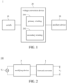
- FIG. 1 is a block diagram illustrating a forward converter according to an embodiment of the present disclosure.
- the forward converter 1 includes a switch 10, a voltage conversion device 20 and an auxiliary device 30.
- the switch 10 is connected to the voltage conversion device 20, and the voltage conversion device 20 is connected to the auxiliary device 30.
- the switch 10 is configured to be switched to make the voltage conversion device 20 receive or not receive an input voltage.
- the switch 10 may be an active power switch element, and is configured to be triggered to be cut off or turned on, so that the voltage conversion device 20 receives or does not receive the input voltage.
- the voltage conversion device 20 includes a primary winding 201 and a secondary winding 202, and the voltage conversion device 20 is configured to convert the input voltage into the output voltage.
- the primary winding 201 and the secondary winding 202 each includes one or more coils.
- the voltage conversion device 20 may further include a fly wheeling diode, an energy storage inductor and an output capacitor.
- a first terminal of the energy storage inductor may be configured to output the output voltage.
- a cathode of the fly wheeling diode and a second terminal of the energy storage inductor may be commonly connected to a first node, and the first node may be connected to the auxiliary device 30.
- a terminal of the output capacitor may be connected to another terminal of the energy storage inductor, and another terminal of the output capacitor may be connected to an anode of the fly wheeling diode.
- the auxiliary device 30 may include one or more passive elements.
- a terminal of the auxiliary device 30 is connected to the secondary winding 202, and another terminal of the auxiliary device 30 is connected to the second terminal of the energy storage inductor of the voltage conversion device 20.
- a terminal of the auxiliary device 30 may be configured to receive the input voltage, and another terminal of the auxiliary device 30 is connected to the primary winding 201.
- the forward converter may have the function of demagnetization and may provide the compensation voltage when the switch is turned on. Specifically, in the application of an alternating current input, the compensation voltage may ease the situation of current dead zone.
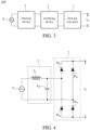
- FIG. 2 is a block diagram illustrating a forward power factor corrector according to an embodiment of the present disclosure.
- the forward power factor corrector 100 includes a forward converter 1 and a rectifying device 2.
- the forward converter 1 may be the forward converter 1 shown in FIG. 1 .
- the rectifying device 2 is connected to a power source V s and the forward converter 1.
- the rectifying device 2 is configured to receive and rectify the power source V s to generate the input voltage described above.
- the power source V s may provide alternating current
- the alternating current is converted into a direct current by the rectifying device 2, and the direct current is provided to the forward converter 1.
- the forward converter 1 converts the input voltage into the output voltage V o , wherein the output voltage V o may be output to a load connected to the forward converter 1.
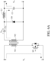
- FIG. 3 is a block diagram illustrating a forward power factor corrector according to another embodiment of the present disclosure.
- the forward power factor corrector 100' includes a forward converter 1, a rectifying device 2 and a filtering device 3.
- the rectifying device 2 is connected to the forward converter 1 and the filtering device 3, wherein the connection and operation of the forward converter 1 and the rectifying device 2 are the same as the embodiment described above, and their detail descriptions are not repeated herein.
- the filtering device 3 is connected between the rectifying device 2 and the power source V s , to first filter the alternating current and then transmit the filtered alternating current to the rectifying device 2 to perform alternating current-direct current conversion.
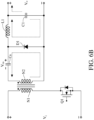
- FIG. 4 exemplarily illustrates circuit diagrams of the rectifying device 2 and the filtering device 3 included in the forward power factor corrector 100' of FIG. 3 .
- the rectifying device 2 may include a first diode D 21 , a second diode D 22 , a third diode D 23 and a fourth diode D 24 .
- An anode of the first diode D 21 is connected to a cathode of the third diode D 23 .
- a cathode of the first diode D 21 is connected to a cathode of the second diode D 22 .
- the filtering device 3 may include a capacitor D f and an inductor L ⁇ .
- a first terminal of the capacitor D f is connected to a first terminal of the inductor L f , an anode of the first diode D 21 and a cathode of the third diode D 23 .
- a second terminal of the capacitor D f is connected to the power source V s , an anode of the second diode D 22 and a cathode of the fourth diode D 24 .
- a second terminal of the inductor L f is connected to the power source V s .
- the filtering device 3 is configured to receive and filter the power source V s to generate the filtered power source V s .
- the rectifying device 2 is configured to receive and rectify the filtered power source V s to form the input voltage V i between the cathode of the second diode D 22 and the anode of the fourth diode D24.
- the forward converter 1 converts the input voltage V i into the output voltage V o , wherein the output voltage V o may be output to a load connected to the forward converter 1.
- FIG. 4 illustrates the basic circuit for implementing the rectifying device 2 and the filtering device 3, FIG. 4 does not intend to limit that the rectifying device 2 and the filtering device 3 can only be implemented by the circuit structure shown in FIG. 4 .
- the filtering device 3 shown in FIG. 4 is selectively disposed.
- FIG. 5 is a circuit diagram of illustrating the forward converter according to a first embodiment of the present disclosure.
- the forward converter 1_1 includes a switch 10_1, a voltage conversion device 20_1 and an auxiliary device 30_1.
- the switch 10_1 includes an active power switch element Q1.
- the voltage conversion device 20_1 includes a primary winding N1 and a secondary winding N2, the fly wheeling diode D1 as described above, an energy storage inductor L1 and an output capacitor C1.
- the auxiliary device 30_1 includes an auxiliary capacitor Ca.
- the first terminal of the energy storage inductor L1 is configured to output the output voltage V o
- the second terminal of the energy storage inductor L1 is connected to the cathode of the fly wheeling diode D1.
- a terminal of the auxiliary capacitor Ca of the auxiliary device 30_1 is connected to the secondary winding N2, and another terminal of the auxiliary capacitor Ca is connected to the second terminal of the energy storage inductor L1 and the cathode of the fly wheeling diode D1.
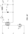
- FIG. 6A to FIG. 6C illustrate a first operation mode, a second operation mode and a third operation mode of the forward converter of FIG. 5 , respectively.
- the active power switch element Q1 in the first operation mode, the active power switch element Q1 is turned on, and the fly wheeling diode D1 is cut off.
- the input voltage V i is provided to the primary winding N1 of the voltage conversion device 20_1, the induced voltage of the secondary winding N2 and the compensation voltage V ca of the auxiliary capacitor Ca of the voltage conversion device 20_1 both charge the output capacitor C1.
- the energy storage inductor L1 stores energy, the auxiliary capacitor Ca is in a discharge state. This operation mode continues until the active power switch element Q1 is cut off, and the second operation mode is entered.
- the active power switch element Q1 is cut off, and the fly wheeling diode D1 is turned on.
- the magnetized secondary winding N2 may be demagnetized through the path formed from the fly wheeling diode D1 to the auxiliary capacitor Ca, and the auxiliary capacitor Ca may be charged to build the compensation voltage V ca .
- the energy storage inductor L1 may release energy through the path formed from the output capacitor C1 and the fly wheeling diode D1. This operation mode continues until the secondary winding N2 and the energy storage inductor L1 discharge all energy, and the third operation mode is entered.
- the forward converter 1_1 returns to the first operation mode of FIG. 6A .
- the third operation mode may not need to exist. That is, after the second operation mode, the operation may directly return to the first operation mode.
- FIG. 7 is a circuit diagram of illustrating the forward converter according to a second embodiment of the present disclosure.
- the forward converter 1_2 includes a switch 10_2, a voltage conversion device 20_2 and an auxiliary device 30_2, wherein circuit/device implementations, functions and connections of the switch 10_2 and the voltage conversion device 20_2 may all be the same as the switch 10_1 and the voltage conversion device 20_1 included in the forward converter 1_1 of FIG. 5 .
- the auxiliary device 30_2 includes an auxiliary capacitor Ca, an auxiliary diode Da1 and an auxiliary winding La1.
- An anode of the auxiliary diode Da1 is connected to the first terminal of the auxiliary capacitor Ca.
- the auxiliary winding La1 is inductively coupled to the energy storage inductor L1 of the voltage conversion device 20_2.
- a terminal of the auxiliary winding La1 is connected to the cathode of the auxiliary diode Da1, and another terminal of the auxiliary winding La1 is connected to the second terminal of the auxiliary capacitor Ca.
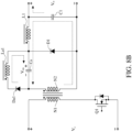
- FIG. 8A to FIG. 8D illustrate a first operation mode, a second operation mode, a third operation mode and a fourth operation mode of the forward converter of FIG. 7 , respectively.
- the active power switch element Q1 is turned on, the auxiliary diode Da1 is cut off, the fly wheeling diode D1 is cut off.
- the input voltage V i is provided to the primary winding N1 of the voltage conversion device 20_2.
- the induced voltage of the secondary winding N2 and the compensation voltage V ca of the auxiliary capacitor Ca of the voltage conversion device 20_2 both charge the output capacitor C1.
- the energy storage inductor L1 stores energy
- the auxiliary capacitor Ca is in a discharge state
- the compensation voltage V ca deceases. This operation mode continues until the active power switch element Q1 is cut off, and the second operation mode is entered.
- the active power switch element Q1 is cut off, the auxiliary diode Da1 is turned on, the fly wheeling diode D1 is cut off.
- the magnetized secondary winding N2 may be demagnetized through the path formed from the auxiliary diode Da1 to the auxiliary capacitor Ca, and the auxiliary capacitor Ca may be charged to build the compensation voltage V ca , and the compensation voltage V ca increases.
- the energy storage inductor L1 may discharge stored energy to the auxiliary capacitor Ca through the auxiliary winding La1.
- This operation mode continues until the compensation voltage V ca is equal to the first mapped voltage, and the third operation mode is entered.
- the first mapped voltage is an equivalent voltage of the output voltage V o mapped to the auxiliary winding La1 side according to a turn ratio of the energy storage inductor L1 and the auxiliary winding La1.
- the active power switch element Q1 is cut off, the auxiliary diode Da1 is cut off, the fly wheeling diode D1 is turned on.
- the magnetized secondary winding N2 is continuously demagnetized through the path formed from the fly wheeling diode D1 to the auxiliary capacitor Ca, and the auxiliary capacitor Ca may be charged to build the compensation voltage V ca .
- the inductor L1 releases the stored energy through the path formed by the fly wheeling diode D1 and the output capacitor C1. This operation mode continues until all energy stored in the energy storage inductor L1 and the magnetized secondary winding N2 is released, and the fourth operation mode is entered.
- the active power switch element Q1, the fly wheeling diode D1 and the auxiliary diode Da1 are cut off, and the forward converter does not perform conversion.
- the energy stored by the output capacitor C1 may continue to provide current to the load.
- the active power switch element Q1 is turned on again, energy stored by the auxiliary capacitor Ca is used to charge the output capacitor C1. That is, the forward converter 1_2 returns to the first operation mode of FIG. 8A .
- the fourth operation mode may not need to exist. That is, after the third operation mode, the operation may directly return to the first operation mode.
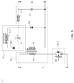
- FIG. 9 is a circuit diagram of illustrating the forward converter according to a third embodiment of the present disclosure.
- the forward converter 1_3 includes a switch 10_3, a voltage conversion device 20_3 and an auxiliary device 30_3, wherein circuit/device implementations, functions and connections of the switch 10_3 and the voltage conversion device 20_3 may all be the same as the switch 10_1 and the voltage conversion device 20_1 included in the forward converter 1_1 of FIG. 5 , and their detail descriptions are not repeated herein.
- the auxiliary device 30_2 includes an auxiliary capacitor Ca, an auxiliary diode Da2 and an auxiliary winding La2.
- An anode of the auxiliary diode Da2 is connected to the first terminal of the auxiliary capacitor Ca.
- the auxiliary winding La2 is inductively coupled to the primary winding N1 and the secondary winding N2.
- a terminal of the auxiliary winding La2 is connected to the cathode of the auxiliary diode Da2, and another terminal of the auxiliary winding La2 is connected to the second terminal of the auxiliary capacitor Ca.
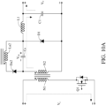
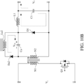
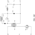
- FIG. 10A to FIG. 10C illustrate a first operation mode, a second operation mode and a third operation mode of the forward converter of FIG. 9 , respectively.
- the active power switch element Q1 is turned on, the auxiliary diode Da2 is cut off, the fly wheeling diode D1 is cut off.
- the input voltage V i is provided to the primary winding N1 of the voltage conversion device 20_3.
- the induced voltage of the secondary winding N2 and the compensation voltage V ca of the auxiliary capacitor Ca of the voltage conversion device 20_3 both charge the output capacitor C1.
- the energy storage inductor L1 stores energy
- the auxiliary capacitor Ca is in a discharge state. This operation mode continues until the active power switch element Q1 is cut off, and the second operation mode is entered.
- the active power switch element Q1 is cut off, the auxiliary diode Da2 is turned on, the fly wheeling diode D1 is cut off. Since the auxiliary winding La2 is inductively coupled to the primary winding N1 and the secondary winding N2, energy stored by the primary winding N1 and the secondary winding N2 may be released through the auxiliary winding La2 to perform demagnetization, and the auxiliary capacitor Ca may be charged to build the compensation voltage V ca .
- the energy storage inductor L1 may release energy through the path formed by the output capacitor C1 and the fly wheeling diode D1. This operation mode continues until said demagnetization is completed, and the energy storage inductor L1 releases all energy.
- the demagnetization performed by the auxiliary winding La2 through the auxiliary diode Da2 and the auxiliary capacitor Ca and the energy release performed by the energy storage inductor L1 through the output capacitor C1 and the fly wheeling diode D1 may be completed at different timings.
- the auxiliary device 30_2 enters the third operation mode.
- the forward converter 1_3 returns to the first operation mode.
- the third operation mode may not need to exist. That is, after the second operation mode, the operation may directly return to the first operation mode.
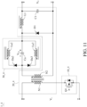
- FIG. 11 is a circuit diagram of illustrating the forward converter according to a fourth embodiment of the present disclosure.
- the forward converter 1_4 includes a switch 10_4, a voltage conversion device 20_4 and an auxiliary device 30_4, wherein circuit/device implementations, functions and connections of the switch 10_4 may all be the same as that of the switch 10_1 included in the forward converter 1_1 of FIG. 5 , and circuit/device implementations, functions and connections of the voltage conversion device 20_4 may all be the same as that of the voltage conversion device 20_2 included in the forward converter 1_2 of FIG. 7 , and their detail descriptions are not repeated herein.
- the auxiliary device 30_4 includes an auxiliary capacitor Ca, a first auxiliary diode Da2, a first auxiliary winding La2, a second auxiliary diode Da3 and a second auxiliary winding La3.
- An anode of the first auxiliary diode Da2 is connected to the first terminal of the auxiliary capacitor Ca.
- the first auxiliary winding La2 is inductively coupled to the primary winding N1 and the secondary winding N2, wherein a terminal of the first auxiliary winding La2 is connected to a cathode of the first auxiliary diode Da2, and another terminal of the first auxiliary winding La2 is connected to the second terminal of the auxiliary capacitor Ca.
- An anode of the second auxiliary diode Da3 is connected to the first terminal of the auxiliary capacitor Ca.
- a terminal of the second auxiliary winding La3 is connected to a cathode of the second auxiliary diode Da3, and another terminal of the second auxiliary winding La3 is connected to the second terminal of the auxiliary capacitor Ca.
- the second auxiliary winding La3 is inductively coupled to the energy storage inductor L1.
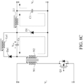
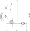
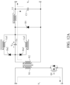
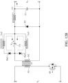
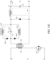
- FIG. 12A to FIG. 12D illustrate a first operation mode, a second operation mode, a third operation mode and a fourth operation mode of the forward converter of FIG. 11 , respectively.
- the active power switch element Q1 in the first operation mode, the active power switch element Q1 is turned on, the first auxiliary diode Da2 is cut off, the second auxiliary diode Da3 is cut off, and the fly wheeling diode D1 is cut off.
- the active power switch element Q1 is turned on, the input voltage V i is provided to the primary winding N1 of the voltage conversion device 20_4.
- the induced voltage of the secondary winding N2 and the compensation voltage V ca of the auxiliary capacitor Ca of voltage conversion device 20_4 both charge the output capacitor C1.
- the energy storage inductor L1 stores energy, the auxiliary capacitor Ca is in a discharge state. This operation mode continues until the active power switch element Q1 is cut off, and the second operation mode is entered.
- the active power switch element Q1 is cut off, the first auxiliary diode Da2 is turned on, the second auxiliary diode Da3 is turned on, the fly wheeling diode D1 is cut off. Since the first auxiliary winding La2 is inductively coupled to the primary winding N1 and the secondary winding N2, by the inductor inductively coupled to the first auxiliary winding La2, the magnetized secondary winding N2 may release energy through the path formed from the first auxiliary diode Da2 to the auxiliary capacitor Ca to perform the demagnetization, and the auxiliary capacitor Ca may be charged to build the compensation voltage V ca .
- the second mapped voltage is an equivalent voltage of the output voltage V o mapped to the second auxiliary winding La3 side according to a turn ratio of the energy storage inductor L1 and the second auxiliary winding La3.
- the active power switch element Q1 is cut off, the first auxiliary diode Da2 is turned on, the second auxiliary diode Da3 is cut off, and the fly wheeling diode D1 is turned on.
- the magnetized secondary winding N2 continues to perform the demagnetization through the path formed from the first auxiliary diode Da2 to the auxiliary capacitor Ca, and continues to charge the auxiliary capacitor Ca to build the compensation voltage V ca .
- the energy storage inductor L1 continues to release energy to charge the output capacitor C1. This operation mode continues until the magnetized secondary winding N2 and energy stored by the energy storage inductor L1 is completely released, and the fourth operation mode is entered.
- the currents on the auxiliary capacitor Ca and the energy storage inductor L1 are reduced to zero, and the first auxiliary diode Da2, the second auxiliary diode Da3 and the fly wheeling diode D1 are all in the cut-off state.
- the energy stored by the output capacitor C1 may continue to provide current to the load.
- the active power switch element Q1 is triggered to be turned on again, energy stored by the auxiliary capacitor Ca is used to charge the output capacitor C1. That is, the forward converter 1_4 returns to the first operation mode.
- the fourth operation mode may not need to exist. That is, after the third operation mode, the operation may directly return to the first operation mode.
- FIG. 13 is a circuit diagram of illustrating the forward converter according to a fifth embodiment of the present disclosure.
- the forward converter 1_5 includes a switch 10_5, a voltage conversion device 20_5 and an auxiliary device 30_5, wherein circuit/device implementations and functions of the switch 10_5 may all be the same as that of the switch 10_1 included in the forward converter 1_1 of FIG. 5 , and their detail descriptions are not repeated herein.
- the voltage conversion device 20_5 of the forward converter 1_5 further includes another fly wheeling diode D2.
- An anode of the fly wheeling diode D2 is connected to the secondary winding N2, and a cathode of the fly wheeling diode D2 is connected to the second terminal of the energy storage inductor L1.
- the auxiliary device 30_5 is disposed at the primary side of the forward converter 1_5. Furthermore, a terminal of the auxiliary device 30_5 is configured to receive the input voltage V i , and another terminal of the auxiliary device 30_5 is connected to the primary winding N1.
- the auxiliary device 30_5 includes an auxiliary capacitor Ca, an auxiliary diode Da4 and an auxiliary winding La4.
- the first terminal of the auxiliary capacitor Ca is configured to receive the input voltage V i
- the second terminal of the auxiliary capacitor Ca is connected to the primary winding N1.
- An anode of the auxiliary diode Da4 is connected to the first terminal of the auxiliary capacitor Ca.
- the auxiliary winding La4 is inductively coupled to the primary winding N1 and the secondary winding N2, wherein a terminal of the auxiliary winding La4 is connected to a cathode of the auxiliary diode Da4, and another terminal of the auxiliary winding La4 is connected to the second terminal of the auxiliary capacitor Ca.
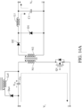
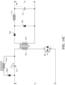
- FIG. 14A to FIG. 14C illustrate a first operation mode, a second operation mode and a third operation mode of the forward converter of FIG. 13 , respectively.
- the active power switch element Q1 is turned on, the auxiliary diode Da4 is cut off, the fly wheeling diode D1 is cut off, and the fly wheeling diode D2 is turned on.
- the input voltage V i and the auxiliary capacitor Ca charge the primary winding N1 of the voltage conversion device 20_5.
- the induced voltage of the secondary winding N2 of the voltage conversion device 20_5 charges the output capacitor C1 through the fly wheeling diode D2.
- the energy storage inductor L1 stores energy, the auxiliary capacitor Ca is in a discharge state. This operation mode continues until the active power switch element Q1 is cut off, and the second operation mode is entered.
- the active power switch element Q1 is cut off, the auxiliary diode Da4 is turned on, the fly wheeling diode D1 is turned on, and the fly wheeling diode D2 is cut off.
- the auxiliary winding La4 is inductively coupled to the primary winding N1 and the secondary winding N2
- energy stored by the primary winding N1 and the secondary winding N2 may be released from the auxiliary winding La4 to perform the demagnetization, and the auxiliary capacitor Ca may be charged to build the compensation voltage V ca .
- the energy storage inductor L1 may release energy through the path formed from the output capacitor C1 and the fly wheeling diode D1.
- the demagnetization performed by the auxiliary winding La4 through the auxiliary diode Da4 and the auxiliary capacitor Ca and the energy release performed by the energy storage inductor L1 through the output capacitor C1 and the fly wheeling diode D1 may be completed at different timings.
- the auxiliary device 30_5 enters the third operation mode.
- the third operation mode energy stored in the primary winding N1 and the secondary winding N2 is completely released, and energy stored in the energy storage inductor L1 is completely released in the second operation mode, the current on the energy storage inductor L1 is reduced to zero, the active power switch element Q1, the fly wheeling diodes D1 and D2 and the auxiliary diode Da4 all enter the cut-off state.
- the active power switch element Q1 is triggered to be turned on again, energy stored by the auxiliary capacitor Ca is used to charge the output capacitor C1. That is, the forward converter 1_5 returns to the first operation mode.
- the energy stored by the output capacitor C1 may continue to provide current to the load.
- the third operation mode may not need to exist. That is, after the second operation mode, the operation may directly return to the first operation mode.
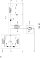
- FIG. 15 is a circuit diagram of illustrating the forward converter according to a sixth embodiment of the present disclosure.
- the forward converter 1_6 includes a switch 10_6, a voltage conversion device 20_6 and an auxiliary device 30_6, wherein circuit/device implementations and functions of the switch 10_6 and the voltage conversion device 20_6 are the same as that of the switch 10_5 and the voltage conversion device 20_5 included in the forward converter 1_5 of FIG. 13 , and their detail descriptions are not repeated herein.
- the auxiliary device 30_6 is disposed at the primary side of the forward converter 1_6.
- the auxiliary device 30_6 includes an auxiliary capacitor Ca, a first auxiliary diode Da4, a second auxiliary diode Da5, a first auxiliary winding La4 and a second auxiliary winding La5.
- the first terminal of the auxiliary capacitor Ca is configured to receive the input voltage V i
- the second terminal of the auxiliary capacitor Ca is connected to the primary winding N1.
- An anode of the first auxiliary diode Da4 is connected to the first terminal of the auxiliary capacitor Ca.
- the first auxiliary winding La4 is inductively coupled to the primary winding N1 and the secondary winding N2.
- a terminal of the first auxiliary winding La4 is connected to a cathode of the first auxiliary diode Da4, and another terminal of the first auxiliary winding La4 is connected to the second terminal of the auxiliary capacitor Ca.
- An anode of the second auxiliary diode Da5 is connected to the first terminal of the auxiliary capacitor Ca.
- the second auxiliary winding La5 is inductively coupled to the energy storage inductor L1.
- a terminal of the second auxiliary winding La5 is connected to a cathode of the second auxiliary diode Da5, and another terminal of the second auxiliary winding La5 is connected to the second terminal of the auxiliary capacitor Ca.
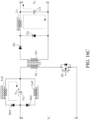
- FIG. 16A to FIG. 16D illustrate a first operation mode, a second operation mode, a third operation mode and a fourth operation mode of the forward converter of FIG. 15 , respectively.
- the active power switch element Q1 is turned on, the first auxiliary diode Da4 is cut off, the second auxiliary diode Da5 is cut off, the fly wheeling diode D1 is cut off, and the fly wheeling diode D2 is turned on.
- the input voltage V i and the auxiliary capacitor Ca charge the primary winding N1 of the voltage conversion device 20_6.
- the induced voltage of the secondary winding N2 of the voltage conversion device 20_6 charges the output capacitor C1.
- the energy storage inductor L1 stores energy, the auxiliary capacitor Ca is in a discharge state. This operation mode continues until the active power switch element Q1 is cut off, and the second operation mode is entered.
- the active power switch element Q1 is cut off, the first auxiliary diode Da4 is turned on, the second auxiliary diode Da5 is turned on, the fly wheeling diodes D1 and D2 are cut off.
- the active power switch element Q1 is cut off, since the first auxiliary winding La4 is inductively coupled to the primary winding N1 and the secondary winding N2, energy stored by the primary winding N1 and the secondary winding N2 may be used to perform the demagnetization through the path formed from the first auxiliary diode Da4 to the auxiliary capacitor Ca, and the auxiliary capacitor Ca may be charged to build the compensation voltage V ca .
- the third mapped voltage is an equivalent voltage of the output voltage V o mapped to the second auxiliary winding La5 side according to a turn ratio of the energy storage inductor L1 and the second auxiliary winding La5.
- the active power switch element Q1 is cut off, the first auxiliary diode Da4 is turned on, the second auxiliary diode Da5 is cut off, the fly wheeling diode D1 is turned on, and the fly wheeling diode D2 is cut off.
- the first auxiliary winding La4 continues to perform the demagnetization through the path formed from the first auxiliary diode Da4 to the auxiliary capacitor Ca, and continues to charge the auxiliary capacitor Ca to build the compensation voltage V ca .
- Energy stored by the energy storage inductor L1 is released through the fly wheeling diode D1 to charge the output capacitor C1. This operation mode continues until energy stored by the first auxiliary winding La4 and the energy storage inductor L1 is completely released, and the fourth operation mode is entered.
- the currents on the auxiliary capacitor Ca and the energy storage inductor L1 are reduced to zero, and the first auxiliary diode Da4, the second auxiliary diode Da5 and the fly wheeling diodes D1 and D2 all enter the cut-off state, and the active power switch element Q1 is still in the cut-off state.
- the energy stored by the output capacitor C1 may continue to provide current to the load.
- the active power switch element Q1 is triggered to be turned on again, energy stored by the auxiliary capacitor Ca is used to charge the output capacitor C1. That is, the forward converter 1_6 returns to the first operation mode.
- the fourth operation mode may not need to exist. That is, after the third operation mode, the operation may directly return to the first operation mode.
- the forward converter and the auxiliary device of the present disclosure may be summarized into various implementations as follows.
- the forward converter and the auxiliary device include the auxiliary capacitor.
- the auxiliary device includes the auxiliary capacitor, the auxiliary diode and the auxiliary winding, wherein the anode of the auxiliary diode is connected to the first terminal of the auxiliary capacitor, the auxiliary winding is inductively coupled to the primary winding and the secondary winding, and a terminal of the auxiliary winding is connected to the cathode of the auxiliary diode, and another terminal of the auxiliary winding is connected to the second terminal of the auxiliary capacitor.
- the voltage conversion device further includes the energy storage inductor configured to output the output voltage
- the auxiliary device includes the auxiliary capacitor, the auxiliary diode and the auxiliary winding, wherein the anode of the auxiliary diode is connected to the first terminal of the auxiliary capacitor, the auxiliary winding is inductively coupled to the energy storage inductor, a terminal of the auxiliary winding is connected to the cathode of the auxiliary diode, and another terminal of the auxiliary winding is connected to the second terminal of the auxiliary capacitor.
- the voltage conversion device further includes the energy storage inductor configured to output the output voltage
- the auxiliary device includes the auxiliary capacitor, the first auxiliary diode, the second auxiliary diode, the first auxiliary winding and the second auxiliary winding, the anode of the first auxiliary diode is connected to the first terminal of the auxiliary capacitor, the first auxiliary winding is inductively coupled to the primary winding and the secondary winding, a terminal of the first auxiliary winding is connected to the cathode of the first auxiliary diode, another terminal of the first auxiliary winding is connected to the second terminal of the auxiliary capacitor, the anode of the second auxiliary diode is connected to the first terminal of the auxiliary capacitor, the second auxiliary winding is inductively coupled to the energy storage inductor, a terminal of the second auxiliary winding is connected to the cathode of the second auxiliary diode, and another terminal of the second auxiliary winding is connected to the second terminal of the auxiliary capacitor.
- the auxiliary device of the above implementations may be connected to the primary winding or the secondary winding, wherein the primary winding is especially adapted to the second implementation to the fourth implementation. It should be noted that by connecting the auxiliary device to the secondary winding, a diode may not need to be disposed between the energy storage inductor and the secondary winding of the voltage conversion device of the forward converter. Therefore, comparing to the structure of the auxiliary device connected to the primary winding, the present disclosure may have a simpler circuit structure.
- FIG. 17 exemplarily presents the waveform diagrams of the voltage and the current at an alternating-current (AC) input terminal the secondary-side current of the forward power factor corrector of the forward converter according to an embodiment of the present disclosure.
- the voltage Vs at the AC input terminal and the current Is at the AC input terminal match each other, there is low current harmonics.
- a demagnetization interval d1 of the secondary-side current I2 it may be known that the forward power factor corrector may effectively perform demagnetization.
- FIG. 18 exemplarily presents relationship between duty cycle of the switch and the output voltage of the forward power factor corrector according to an embodiment of the present disclosure.
- the forward converter may have the advantages of high conversion efficiency, meet the demagnetization requirements of the windings of a voltage converter, be able to provide compensation voltage, be smaller in size and light in weight, and may do so without adding additional complex and high-cost structure.
- the forward power factor corrector including the forward converter described above of the present disclosure in addition to the above advantageous, may also reduce the current dead zone through the compensation voltage of the auxiliary device, and may achieve the effects of high power factor and low harmonic rate.
Landscapes
- Engineering & Computer Science (AREA)
- Power Engineering (AREA)
- Dc-Dc Converters (AREA)
Abstract
A forward converter (1, 1_1, 1_2, 1_3, 1_4, 1_5, 1_6) includes a voltage conversion device (20, 20_1, 20_2, 20_3, 20_4, 20_5, 20_6), a switch (10, 10_1, 10_2, 10_3, 10_4, 10_5, 10_6) and an auxiliary device (30, 30_1, 30_2, 30_3, 30_4, 30_5, 30_6). The voltage conversion device (20, 20_1, 20_2,20_3, 20_4, 20_5,20_6) includes a primary winding (201, N1) and a secondary winding (202, N2), and is configured to convert an input voltage (V<sub>i</sub>) into an output voltage (V<sub>o</sub>). The switch (10, 10_1, 10_2, 10_3, 10_4, 10_5, 10_6) is connected to the voltage conversion device (20, 20_1, 20_2, 20_3, 20_4, 20_5, 20_6), and is switched to make the voltage conversion device (20, 20_1, 20_2, 20_3, 20_4, 20_5, 20_6) receive or not receive the input voltage (V<sub>i</sub>). The auxiliary device (30, 30_1, 30_2, 30_3, 30_4, 30_5, 30_6) is connected to the voltage conversion device (20, 20_1, 20_2, 20_3, 20_4, 20_5, 20_6). When the switch (10, 10_1, 10_2, 10_3, 10_4, 10_5, 10_6) is cut off, the auxiliary device (30, 30_1, 30_2, 30_3, 30_4, 30_5, 30_6) stores electrical energy released by the voltage conversion device (20, 20_1, 20_2, 20_3, 20_4, 20_5, 20_6) and generates a compensation voltage (V<sub>ca</sub>), and when the switch (10, 10_1, 10_2, 10_3, 10_4, 10_5, 10_6) is turned on, the auxiliary device (30, 30_1, 30_2, 30_3, 30_4, 30_5, 30_6) provides the compensation voltage (V<sub>ca</sub>), wherein the compensation voltage (V<sub>ca</sub>) and the input voltage (V<sub>i</sub>) have same polarity. The present disclosure further provides a forward power factor corrector including the forward converter (1, 1_1, 1_2, 1_3, 1_4, 1_5, 1_6) described above and a rectifying device.
Description
- This disclosure relates to a forward converter and forward power factor corrector.
- At present, many electrical appliances use low-voltage direct current. However, since power provided by the supply mains is alternating current (AC), alternating current-direct current conversion is required. In order to reduce the reactive power of the power system and reduce the system interference caused by current harmonics, many electrical appliances are required to have high power factor and low current harmonics, so power factor correctors are widely used.
- Based on safety and performance considerations, power factor correctors are required to have high power factor, high conversion efficiency and electrical isolation. Conventional circuit structures such as fly-back structure have poor conversion efficiency; and for conventional forward circuits, when the input AC power is in a low voltage state, if the induced voltage on the secondary side is less than the output voltage of the power factor corrector, the input current cannot be introduced, resulting in a current dead zone. Therefore, the power factor correction effect is compromised, and additional transformer is needed to deal with demagnetization requirement. Other conventional technologies and circuit structures also face different technical bottlenecks and cannot meet increasingly stringent regulatory requirements.
- Accordingly, this disclosure provides a forward converter and forward power factor corrector.
- According to one or more embodiment of this disclosure, a forward converter includes a voltage conversion device, a switch and an auxiliary device. The voltage conversion device includes a primary winding and a secondary winding and is configured to convert an input voltage into an output voltage. The switch is connected to the voltage conversion device and is configured to be switched to make the voltage conversion device receive or not receive the input voltage. The auxiliary device is connected to the voltage conversion device, stores electrical energy released by the voltage conversion device and generating a compensation voltage when the switch is cut off, and providing the compensation voltage when the switch is turned on, wherein the compensation voltage and the input voltage have same polarity.
- According to one or more embodiment of this disclosure, a forward power factor corrector includes the forward converter described above and a rectifying device connected to the forward converter and configured to receive and rectify a power source to generate the input voltage.
- In view of the above description, with the auxiliary device, the forward converter according to one or more embodiments of the present disclosure may have the advantages of high conversion efficiency, meet the demagnetization requirements of the windings of a voltage converter, be able to provide compensation voltage, be smaller in size and light in weight, and may do so without adding additional complex and high-cost structure. The forward power factor corrector including the forward converter described above of the present disclosure, in addition to the above advantageous, may also reduce the current dead zone through the compensation voltage of the auxiliary device, and may achieve the effects of high power factor and low harmonic rate.
- The present disclosure will become more fully understood from the detailed description given hereinbelow and the accompanying drawings which are given by way of illustration only and thus are not limitative of the present disclosure and wherein:
-
FIG. 1 is a block diagram illustrating a forward converter according to an embodiment of the present disclosure; -
FIG. 2 is a block diagram illustrating a forward power factor corrector according to an embodiment of the present disclosure; -
FIG. 3 is a block diagram illustrating a forward power factor corrector according to another embodiment of the present disclosure; -
FIG. 4 exemplarily illustrates a circuit diagram of a rectifying device and a filtering device included in forward power factor ofFIG. 3 ; -
FIG. 5 is a circuit diagram of illustrating the forward converter according to a first embodiment of the present disclosure; -
FIG. 6A to FIG. 6C illustrate a first operation mode, a second operation mode and a third operation mode of the forward converter ofFIG. 5 , respectively; -
FIG. 7 is a circuit diagram of illustrating the forward converter according to a second embodiment of the present disclosure; -
FIG. 8A to FIG. 8D illustrate a first operation mode, a second operation mode, a third operation mode and a fourth operation mode of the forward converter ofFIG. 7 , respectively; -
FIG. 9 is a circuit diagram of illustrating the forward converter according to a third embodiment of the present disclosure; -
FIG. 10A to FIG. 10C illustrate a first operation mode, a second operation mode and a third operation mode of the forward converter ofFIG. 9 , respectively; -
FIG. 11 is a circuit diagram of illustrating the forward converter according to a fourth embodiment of the present disclosure; -
FIG. 12A to FIG. 12D illustrate a first operation mode, a second operation mode, a third operation mode and a fourth operation mode of the forward converter ofFIG. 11 , respectively; -
FIG. 13 is a circuit diagram of illustrating the forward converter according to a fifth embodiment of the present disclosure; -
FIG. 14A to FIG. 14C illustrate a first operation mode, a second operation mode and a third operation mode of the forward converter ofFIG. 13 , respectively; -
FIG. 15 is a circuit diagram of illustrating the forward converter according to a sixth embodiment of the present disclosure; -
FIG. 16A to FIG. 16D illustrate a first operation mode, a second operation mode, a third operation mode and a fourth operation mode of the forward converter ofFIG. 15 , respectively; -
FIG. 17 exemplarily presents the waveform diagrams of the gate-source voltage, the flowing current and the drain-source voltage of the switch of the forward converter according to an embodiment of the present disclosure; and -
FIG. 18 exemplarily presents the relationship between the output voltage and the switching duty cycle of the forward power factor corrector according to an embodiment of the present disclosure. - In the following detailed description, for purposes of explanation, numerous specific details are set forth in order to provide a thorough understanding of the disclosed embodiments. According to the description, claims and the drawings disclosed in the specification, one skilled in the art may easily understand the concepts and features of the present invention. The following embodiments further illustrate various aspects of the present invention, but are not meant to limit the scope of the present invention.
- Please refer to
FIG. 1 , whereinFIG. 1 is a block diagram illustrating a forward converter according to an embodiment of the present disclosure. As shown inFIG. 1 , theforward converter 1 includes aswitch 10, avoltage conversion device 20 and anauxiliary device 30. Theswitch 10 is connected to thevoltage conversion device 20, and thevoltage conversion device 20 is connected to theauxiliary device 30. - The
switch 10 is configured to be switched to make thevoltage conversion device 20 receive or not receive an input voltage. For example, theswitch 10 may be an active power switch element, and is configured to be triggered to be cut off or turned on, so that thevoltage conversion device 20 receives or does not receive the input voltage. - The
voltage conversion device 20 includes aprimary winding 201 and asecondary winding 202, and thevoltage conversion device 20 is configured to convert the input voltage into the output voltage. Theprimary winding 201 and thesecondary winding 202 each includes one or more coils. In an implementation, thevoltage conversion device 20 may further include a fly wheeling diode, an energy storage inductor and an output capacitor. A first terminal of the energy storage inductor may be configured to output the output voltage. A cathode of the fly wheeling diode and a second terminal of the energy storage inductor may be commonly connected to a first node, and the first node may be connected to theauxiliary device 30. A terminal of the output capacitor may be connected to another terminal of the energy storage inductor, and another terminal of the output capacitor may be connected to an anode of the fly wheeling diode. - The
auxiliary device 30 may include one or more passive elements. A terminal of theauxiliary device 30 is connected to the secondary winding 202, and another terminal of theauxiliary device 30 is connected to the second terminal of the energy storage inductor of thevoltage conversion device 20. Alternatively, a terminal of theauxiliary device 30 may be configured to receive the input voltage, and another terminal of theauxiliary device 30 is connected to the primary winding 201. When theswitch 10 is cut off, theauxiliary device 30 stores energy released by thevoltage conversion device 20 and generates a compensation voltage; and when theswitch 10 is turned on, theauxiliary device 30 provides the compensation voltage, wherein the compensation voltage and the input voltage have same polarity. - By storing energy released by the voltage conversion device when the switch is cut off and generating the compensation voltage, the forward converter may have the function of demagnetization and may provide the compensation voltage when the switch is turned on. Specifically, in the application of an alternating current input, the compensation voltage may ease the situation of current dead zone.
- Please refer to
FIG. 2 , whereinFIG. 2 is a block diagram illustrating a forward power factor corrector according to an embodiment of the present disclosure. As shown inFIG. 2 , the forwardpower factor corrector 100 includes aforward converter 1 and arectifying device 2. Theforward converter 1 may be theforward converter 1 shown inFIG. 1 . The rectifyingdevice 2 is connected to a power source Vs and theforward converter 1. The rectifyingdevice 2 is configured to receive and rectify the power source Vs to generate the input voltage described above. Specifically, the power source Vs may provide alternating current, the alternating current is converted into a direct current by the rectifyingdevice 2, and the direct current is provided to theforward converter 1. Theforward converter 1 converts the input voltage into the output voltage Vo, wherein the output voltage Vo may be output to a load connected to theforward converter 1. - Please refer to
FIG. 3 , whereinFIG. 3 is a block diagram illustrating a forward power factor corrector according to another embodiment of the present disclosure. As shown inFIG. 3 , the forward power factor corrector 100' includes aforward converter 1, a rectifyingdevice 2 and afiltering device 3. The rectifyingdevice 2 is connected to theforward converter 1 and thefiltering device 3, wherein the connection and operation of theforward converter 1 and the rectifyingdevice 2 are the same as the embodiment described above, and their detail descriptions are not repeated herein. In this embodiment, thefiltering device 3 is connected between the rectifyingdevice 2 and the power source Vs, to first filter the alternating current and then transmit the filtered alternating current to therectifying device 2 to perform alternating current-direct current conversion. - To further explain circuits of the
filtering device 3 and the rectifyingdevice 2, please refer toFIG. 4 , whereinFIG. 4 exemplarily illustrates circuit diagrams of the rectifyingdevice 2 and thefiltering device 3 included in the forward power factor corrector 100' ofFIG. 3 . As shown inFIG. 4 , the rectifyingdevice 2 may include a first diode D21, a second diode D22, a third diode D23 and a fourth diode D24. An anode of the first diode D21 is connected to a cathode of the third diode D23. A cathode of the first diode D21 is connected to a cathode of the second diode D22. An anode of the second diode D22 is connected to a cathode of the fourth diode D24. An anode of the third diode D23 is connected to an anode of the fourth diode D24. Thefiltering device 3 may include a capacitor Df and an inductor Lε. A first terminal of the capacitor Df is connected to a first terminal of the inductor Lf, an anode of the first diode D21 and a cathode of the third diode D23. A second terminal of the capacitor Df is connected to the power source Vs, an anode of the second diode D22 and a cathode of the fourth diode D24. A second terminal of the inductor Lf is connected to the power source Vs. - The
filtering device 3 is configured to receive and filter the power source Vs to generate the filtered power source Vs. The rectifyingdevice 2 is configured to receive and rectify the filtered power source Vs to form the input voltage Vi between the cathode of the second diode D22 and the anode of the fourth diode D24. Theforward converter 1 converts the input voltage Vi into the output voltage Vo, wherein the output voltage Vo may be output to a load connected to theforward converter 1. It should be noted thatFIG. 4 illustrates the basic circuit for implementing the rectifyingdevice 2 and thefiltering device 3,FIG. 4 does not intend to limit that the rectifyingdevice 2 and thefiltering device 3 can only be implemented by the circuit structure shown inFIG. 4 . In addition, thefiltering device 3 shown inFIG. 4 is selectively disposed. - The following further explains embodiments for implementing the
forward converter 1 described above. Please refer toFIG. 5 , whereinFIG. 5 is a circuit diagram of illustrating the forward converter according to a first embodiment of the present disclosure. As shown inFIG. 5 , the forward converter 1_1 includes a switch 10_1, a voltage conversion device 20_1 and an auxiliary device 30_1. - The switch 10_1 includes an active power switch element Q1. The voltage conversion device 20_1 includes a primary winding N1 and a secondary winding N2, the fly wheeling diode D1 as described above, an energy storage inductor L1 and an output capacitor C1. The auxiliary device 30_1 includes an auxiliary capacitor Ca.
- Specifically, the first terminal of the energy storage inductor L1 is configured to output the output voltage Vo, and the second terminal of the energy storage inductor L1 is connected to the cathode of the fly wheeling diode D1. A terminal of the auxiliary capacitor Ca of the auxiliary device 30_1 is connected to the secondary winding N2, and another terminal of the auxiliary capacitor Ca is connected to the second terminal of the energy storage inductor L1 and the cathode of the fly wheeling diode D1.
- Please refer to
FIG. 5 along withFIG. 6A to FIG. 6C , whereinFIG. 6A to FIG. 6C illustrate a first operation mode, a second operation mode and a third operation mode of the forward converter ofFIG. 5 , respectively. - Please refer to
FIG. 6A , in the first operation mode, the active power switch element Q1 is turned on, and the fly wheeling diode D1 is cut off. When the active power switch element Q1 is turned on, the input voltage Vi is provided to the primary winding N1 of the voltage conversion device 20_1, the induced voltage of the secondary winding N2 and the compensation voltage Vca of the auxiliary capacitor Ca of the voltage conversion device 20_1 both charge the output capacitor C1. At the same time, the energy storage inductor L1 stores energy, the auxiliary capacitor Ca is in a discharge state. This operation mode continues until the active power switch element Q1 is cut off, and the second operation mode is entered. - Please refer to
FIG. 6B , in the second operation mode, the active power switch element Q1 is cut off, and the fly wheeling diode D1 is turned on. The magnetized secondary winding N2 may be demagnetized through the path formed from the fly wheeling diode D1 to the auxiliary capacitor Ca, and the auxiliary capacitor Ca may be charged to build the compensation voltage Vca. The energy storage inductor L1 may release energy through the path formed from the output capacitor C1 and the fly wheeling diode D1. This operation mode continues until the secondary winding N2 and the energy storage inductor L1 discharge all energy, and the third operation mode is entered. - Please refer to
FIG. 6C , in the third operation mode, the active power switch element Q1 and the fly wheeling diode D1 are cut off, the forward converter does not perform conversion. The energy stored by the output capacitor C1 may continue to provide current to the load. Then, when the active power switch element Q1 is turned on again, the energy stored by the auxiliary capacitor Ca is used to charge the output capacitor C1. That is, the forward converter 1_1 returns to the first operation mode ofFIG. 6A . In particular, in an application where the forward converter of this embodiment is designed to operate in continuous current mode, the third operation mode may not need to exist. That is, after the second operation mode, the operation may directly return to the first operation mode. - Please refer to
FIG. 7 , whereinFIG. 7 is a circuit diagram of illustrating the forward converter according to a second embodiment of the present disclosure. As shown inFIG. 7 , the forward converter 1_2 includes a switch 10_2, a voltage conversion device 20_2 and an auxiliary device 30_2, wherein circuit/device implementations, functions and connections of the switch 10_2 and the voltage conversion device 20_2 may all be the same as the switch 10_1 and the voltage conversion device 20_1 included in the forward converter 1_1 ofFIG. 5 . - The auxiliary device 30_2 includes an auxiliary capacitor Ca, an auxiliary diode Da1 and an auxiliary winding La1. An anode of the auxiliary diode Da1 is connected to the first terminal of the auxiliary capacitor Ca. The auxiliary winding La1 is inductively coupled to the energy storage inductor L1 of the voltage conversion device 20_2. A terminal of the auxiliary winding La1 is connected to the cathode of the auxiliary diode Da1, and another terminal of the auxiliary winding La1 is connected to the second terminal of the auxiliary capacitor Ca.
- Please refer to
FIG. 7 andFIG. 8A toFIG. 8D , whereinFIG. 8A to FIG. 8D illustrate a first operation mode, a second operation mode, a third operation mode and a fourth operation mode of the forward converter ofFIG. 7 , respectively. - Please refer to
FIG. 8A , in the first operation mode, the active power switch element Q1 is turned on, the auxiliary diode Da1 is cut off, the fly wheeling diode D1 is cut off. When the active power switch element Q1 is turned on, the input voltage Vi is provided to the primary winding N1 of the voltage conversion device 20_2. The induced voltage of the secondary winding N2 and the compensation voltage Vca of the auxiliary capacitor Ca of the voltage conversion device 20_2 both charge the output capacitor C1. At the same time, the energy storage inductor L1 stores energy, the auxiliary capacitor Ca is in a discharge state, and the compensation voltage Vca deceases. This operation mode continues until the active power switch element Q1 is cut off, and the second operation mode is entered. - Please refer to
FIG. 8B , in the second operation mode, the active power switch element Q1 is cut off, the auxiliary diode Da1 is turned on, the fly wheeling diode D1 is cut off. The magnetized secondary winding N2 may be demagnetized through the path formed from the auxiliary diode Da1 to the auxiliary capacitor Ca, and the auxiliary capacitor Ca may be charged to build the compensation voltage Vca, and the compensation voltage Vca increases. The energy storage inductor L1 may discharge stored energy to the auxiliary capacitor Ca through the auxiliary winding La1. This operation mode continues until the compensation voltage Vca is equal to the first mapped voltage, and the third operation mode is entered. The first mapped voltage is an equivalent voltage of the output voltage Vo mapped to the auxiliary winding La1 side according to a turn ratio of the energy storage inductor L1 and the auxiliary winding La1. - Please refer to
FIG. 8C , in the third operation mode, the active power switch element Q1 is cut off, the auxiliary diode Da1 is cut off, the fly wheeling diode D1 is turned on. The magnetized secondary winding N2 is continuously demagnetized through the path formed from the fly wheeling diode D1 to the auxiliary capacitor Ca, and the auxiliary capacitor Ca may be charged to build the compensation voltage Vca. The inductor L1 releases the stored energy through the path formed by the fly wheeling diode D1 and the output capacitor C1. This operation mode continues until all energy stored in the energy storage inductor L1 and the magnetized secondary winding N2 is released, and the fourth operation mode is entered. - Please refer to
FIG. 8D , in the fourth operation mode, the active power switch element Q1, the fly wheeling diode D1 and the auxiliary diode Da1 are cut off, and the forward converter does not perform conversion. The energy stored by the output capacitor C1 may continue to provide current to the load. Then, when the active power switch element Q1 is turned on again, energy stored by the auxiliary capacitor Ca is used to charge the output capacitor C1. That is, the forward converter 1_2 returns to the first operation mode ofFIG. 8A . In particular, in an application where the forward converter of this embodiment is designed to operate in continuous current mode, the fourth operation mode may not need to exist. That is, after the third operation mode, the operation may directly return to the first operation mode. - Please refer to
FIG. 9 , whereinFIG. 9 is a circuit diagram of illustrating the forward converter according to a third embodiment of the present disclosure. As shown inFIG. 9 , the forward converter 1_3 includes a switch 10_3, a voltage conversion device 20_3 and an auxiliary device 30_3, wherein circuit/device implementations, functions and connections of the switch 10_3 and the voltage conversion device 20_3 may all be the same as the switch 10_1 and the voltage conversion device 20_1 included in the forward converter 1_1 ofFIG. 5 , and their detail descriptions are not repeated herein. - The auxiliary device 30_2 includes an auxiliary capacitor Ca, an auxiliary diode Da2 and an auxiliary winding La2. An anode of the auxiliary diode Da2 is connected to the first terminal of the auxiliary capacitor Ca. The auxiliary winding La2 is inductively coupled to the primary winding N1 and the secondary winding N2. A terminal of the auxiliary winding La2 is connected to the cathode of the auxiliary diode Da2, and another terminal of the auxiliary winding La2 is connected to the second terminal of the auxiliary capacitor Ca.
- Please refer to
FIG. 9 andFIG. 10A toFIG. 10C , whereinFIG. 10A to FIG. 10C illustrate a first operation mode, a second operation mode and a third operation mode of the forward converter ofFIG. 9 , respectively. - Please refer to
FIG. 10A , in the first operation mode, the active power switch element Q1 is turned on, the auxiliary diode Da2 is cut off, the fly wheeling diode D1 is cut off. When the active power switch element Q1 is turned on, the input voltage Vi is provided to the primary winding N1 of the voltage conversion device 20_3. The induced voltage of the secondary winding N2 and the compensation voltage Vca of the auxiliary capacitor Ca of the voltage conversion device 20_3 both charge the output capacitor C1. At the same time, the energy storage inductor L1 stores energy, the auxiliary capacitor Ca is in a discharge state. This operation mode continues until the active power switch element Q1 is cut off, and the second operation mode is entered. - Please refer to
FIG. 10B , in the second operation mode, the active power switch element Q1 is cut off, the auxiliary diode Da2 is turned on, the fly wheeling diode D1 is cut off. Since the auxiliary winding La2 is inductively coupled to the primary winding N1 and the secondary winding N2, energy stored by the primary winding N1 and the secondary winding N2 may be released through the auxiliary winding La2 to perform demagnetization, and the auxiliary capacitor Ca may be charged to build the compensation voltage Vca. The energy storage inductor L1 may release energy through the path formed by the output capacitor C1 and the fly wheeling diode D1. This operation mode continues until said demagnetization is completed, and the energy storage inductor L1 releases all energy. In particular, in some implementations, the demagnetization performed by the auxiliary winding La2 through the auxiliary diode Da2 and the auxiliary capacitor Ca and the energy release performed by the energy storage inductor L1 through the output capacitor C1 and the fly wheeling diode D1 may be completed at different timings. When the demagnetization of the auxiliary winding La2 and the energy release of the energy storage inductor L1 are both completed, the auxiliary device 30_2 enters the third operation mode. - Please refer to
FIG. 10C , in the third operation mode, since energy stored by the energy storage inductor L1 is completely released, the current on the energy storage inductor L1 is reduced to zero, and after energy is completely released from the magnetized secondary winding N2 in the second operation mode, the current on the auxiliary capacitor Ca is reduced to zero, and the fly wheeling diode D1 and the auxiliary diode Da2 both enter the cut-off state, and the active power switch element Q1 is still in the cut-off state. The energy stored by the output capacitor C1 may continue to provide current to the load. When the active power switch element Q1 is triggered to be turned on again, energy stored by the auxiliary capacitor Ca is used to charge the output capacitor C1. That is, the forward converter 1_3 returns to the first operation mode. In particular, in the application where the forward converter of this embodiment is designed to operate in continuous current mode, the third operation mode may not need to exist. That is, after the second operation mode, the operation may directly return to the first operation mode. - Please refer to
FIG. 11 , whereinFIG. 11 is a circuit diagram of illustrating the forward converter according to a fourth embodiment of the present disclosure. As shown inFIG. 11 , the forward converter 1_4 includes a switch 10_4, a voltage conversion device 20_4 and an auxiliary device 30_4, wherein circuit/device implementations, functions and connections of the switch 10_4 may all be the same as that of the switch 10_1 included in the forward converter 1_1 ofFIG. 5 , and circuit/device implementations, functions and connections of the voltage conversion device 20_4 may all be the same as that of the voltage conversion device 20_2 included in the forward converter 1_2 ofFIG. 7 , and their detail descriptions are not repeated herein. - The auxiliary device 30_4 includes an auxiliary capacitor Ca, a first auxiliary diode Da2, a first auxiliary winding La2, a second auxiliary diode Da3 and a second auxiliary winding La3. An anode of the first auxiliary diode Da2 is connected to the first terminal of the auxiliary capacitor Ca. The first auxiliary winding La2 is inductively coupled to the primary winding N1 and the secondary winding N2, wherein a terminal of the first auxiliary winding La2 is connected to a cathode of the first auxiliary diode Da2, and another terminal of the first auxiliary winding La2 is connected to the second terminal of the auxiliary capacitor Ca. An anode of the second auxiliary diode Da3 is connected to the first terminal of the auxiliary capacitor Ca. A terminal of the second auxiliary winding La3 is connected to a cathode of the second auxiliary diode Da3, and another terminal of the second auxiliary winding La3 is connected to the second terminal of the auxiliary capacitor Ca. The second auxiliary winding La3 is inductively coupled to the energy storage inductor L1.
- Please refer to
FIG. 11 andFIG. 12A toFIG. 12D , whereinFIG. 12A to FIG. 12D illustrate a first operation mode, a second operation mode, a third operation mode and a fourth operation mode of the forward converter ofFIG. 11 , respectively. - Please refer to
FIG. 12A , in the first operation mode, the active power switch element Q1 is turned on, the first auxiliary diode Da2 is cut off, the second auxiliary diode Da3 is cut off, and the fly wheeling diode D1 is cut off. When the active power switch element Q1 is turned on, the input voltage Vi is provided to the primary winding N1 of the voltage conversion device 20_4. The induced voltage of the secondary winding N2 and the compensation voltage Vca of the auxiliary capacitor Ca of voltage conversion device 20_4 both charge the output capacitor C1. At the same time, the energy storage inductor L1 stores energy, the auxiliary capacitor Ca is in a discharge state. This operation mode continues until the active power switch element Q1 is cut off, and the second operation mode is entered. - Please refer to
FIG. 12B , in the second operation mode, the active power switch element Q1 is cut off, the first auxiliary diode Da2 is turned on, the second auxiliary diode Da3 is turned on, the fly wheeling diode D1 is cut off. Since the first auxiliary winding La2 is inductively coupled to the primary winding N1 and the secondary winding N2, by the inductor inductively coupled to the first auxiliary winding La2, the magnetized secondary winding N2 may release energy through the path formed from the first auxiliary diode Da2 to the auxiliary capacitor Ca to perform the demagnetization, and the auxiliary capacitor Ca may be charged to build the compensation voltage Vca. Since the second auxiliary winding La3 is inductively coupled to the energy storage inductor L1, energy stored by the energy storage inductor L1 may be released from the second auxiliary winding La3 to charge the auxiliary capacitor Ca. Therefore, the compensation voltage Vca increases. This operation mode continues until the compensation voltage Vca is equal to the second mapped voltage, and the third operation mode is entered. The second mapped voltage is an equivalent voltage of the output voltage Vo mapped to the second auxiliary winding La3 side according to a turn ratio of the energy storage inductor L1 and the second auxiliary winding La3. - Please refer to
FIG. 12C , in the third operation mode, the active power switch element Q1 is cut off, the first auxiliary diode Da2 is turned on, the second auxiliary diode Da3 is cut off, and the fly wheeling diode D1 is turned on. The magnetized secondary winding N2 continues to perform the demagnetization through the path formed from the first auxiliary diode Da2 to the auxiliary capacitor Ca, and continues to charge the auxiliary capacitor Ca to build the compensation voltage Vca. The energy storage inductor L1 continues to release energy to charge the output capacitor C1. This operation mode continues until the magnetized secondary winding N2 and energy stored by the energy storage inductor L1 is completely released, and the fourth operation mode is entered. - Please refer to
FIG. 12D , after the magnetized secondary winding N2 and the energy storage inductor L1 completely releases the stored energy in the third operation mode, the currents on the auxiliary capacitor Ca and the energy storage inductor L1 are reduced to zero, and the first auxiliary diode Da2, the second auxiliary diode Da3 and the fly wheeling diode D1 are all in the cut-off state. The energy stored by the output capacitor C1 may continue to provide current to the load. When the active power switch element Q1 is triggered to be turned on again, energy stored by the auxiliary capacitor Ca is used to charge the output capacitor C1. That is, the forward converter 1_4 returns to the first operation mode. In particular, in an application where the forward converter of this embodiment is designed to operate in continuous current mode, the fourth operation mode may not need to exist. That is, after the third operation mode, the operation may directly return to the first operation mode. - Please refer to
FIG. 13 , whereinFIG. 13 is a circuit diagram of illustrating the forward converter according to a fifth embodiment of the present disclosure. As shown inFIG. 13 , the forward converter 1_5 includes a switch 10_5, a voltage conversion device 20_5 and an auxiliary device 30_5, wherein circuit/device implementations and functions of the switch 10_5 may all be the same as that of the switch 10_1 included in the forward converter 1_1 ofFIG. 5 , and their detail descriptions are not repeated herein. - In addition to the elements of the voltage conversion device 20_1 shown in
FIG. 5 , the voltage conversion device 20_5 of the forward converter 1_5 further includes another fly wheeling diode D2. An anode of the fly wheeling diode D2 is connected to the secondary winding N2, and a cathode of the fly wheeling diode D2 is connected to the second terminal of the energy storage inductor L1. - The auxiliary device 30_5 is disposed at the primary side of the forward converter 1_5. Furthermore, a terminal of the auxiliary device 30_5 is configured to receive the input voltage Vi, and another terminal of the auxiliary device 30_5 is connected to the primary winding N1. The auxiliary device 30_5 includes an auxiliary capacitor Ca, an auxiliary diode Da4 and an auxiliary winding La4. The first terminal of the auxiliary capacitor Ca is configured to receive the input voltage Vi, and the second terminal of the auxiliary capacitor Ca is connected to the primary winding N1. An anode of the auxiliary diode Da4 is connected to the first terminal of the auxiliary capacitor Ca. The auxiliary winding La4 is inductively coupled to the primary winding N1 and the secondary winding N2, wherein a terminal of the auxiliary winding La4 is connected to a cathode of the auxiliary diode Da4, and another terminal of the auxiliary winding La4 is connected to the second terminal of the auxiliary capacitor Ca.
- Please refer to
FIG. 13 andFIG. 14A toFIG. 14C , whereinFIG. 14A to FIG. 14C illustrate a first operation mode, a second operation mode and a third operation mode of the forward converter ofFIG. 13 , respectively. - Please refer to
FIG. 14A , in the first operation mode, the active power switch element Q1 is turned on, the auxiliary diode Da4 is cut off, the fly wheeling diode D1 is cut off, and the fly wheeling diode D2 is turned on. When the active power switch element Q1 is turned on, the input voltage Vi and the auxiliary capacitor Ca charge the primary winding N1 of the voltage conversion device 20_5. The induced voltage of the secondary winding N2 of the voltage conversion device 20_5 charges the output capacitor C1 through the fly wheeling diode D2. At the same time, the energy storage inductor L1 stores energy, the auxiliary capacitor Ca is in a discharge state. This operation mode continues until the active power switch element Q1 is cut off, and the second operation mode is entered. - Please refer to
FIG. 14B , in the second operation mode, the active power switch element Q1 is cut off, the auxiliary diode Da4 is turned on, the fly wheeling diode D1 is turned on, and the fly wheeling diode D2 is cut off. Since the auxiliary winding La4 is inductively coupled to the primary winding N1 and the secondary winding N2, energy stored by the primary winding N1 and the secondary winding N2 may be released from the auxiliary winding La4 to perform the demagnetization, and the auxiliary capacitor Ca may be charged to build the compensation voltage Vca. The energy storage inductor L1 may release energy through the path formed from the output capacitor C1 and the fly wheeling diode D1. This operation mode continues until said demagnetization is completed, and the energy storage inductor L1 releases all energy. In particular, in some implementations, the demagnetization performed by the auxiliary winding La4 through the auxiliary diode Da4 and the auxiliary capacitor Ca and the energy release performed by the energy storage inductor L1 through the output capacitor C1 and the fly wheeling diode D1 may be completed at different timings. When the demagnetization of the auxiliary winding La4 and the energy release of the energy storage inductor L1 are both completed, the auxiliary device 30_5 enters the third operation mode. - Please refer to
FIG. 14C , in the third operation mode, energy stored in the primary winding N1 and the secondary winding N2 is completely released, and energy stored in the energy storage inductor L1 is completely released in the second operation mode, the current on the energy storage inductor L1 is reduced to zero, the active power switch element Q1, the fly wheeling diodes D1 and D2 and the auxiliary diode Da4 all enter the cut-off state. When the active power switch element Q1 is triggered to be turned on again, energy stored by the auxiliary capacitor Ca is used to charge the output capacitor C1. That is, the forward converter 1_5 returns to the first operation mode. The energy stored by the output capacitor C1 may continue to provide current to the load. In particular, in an application where the forward converter of this embodiment is designed to operate in continuous current mode, the third operation mode may not need to exist. That is, after the second operation mode, the operation may directly return to the first operation mode. - Please refer to
FIG. 15 , whereinFIG. 15 is a circuit diagram of illustrating the forward converter according to a sixth embodiment of the present disclosure. As shown inFIG. 15 , the forward converter 1_6 includes a switch 10_6, a voltage conversion device 20_6 and an auxiliary device 30_6, wherein circuit/device implementations and functions of the switch 10_6 and the voltage conversion device 20_6 are the same as that of the switch 10_5 and the voltage conversion device 20_5 included in the forward converter 1_5 ofFIG. 13 , and their detail descriptions are not repeated herein. - The auxiliary device 30_6 is disposed at the primary side of the forward converter 1_6. The auxiliary device 30_6 includes an auxiliary capacitor Ca, a first auxiliary diode Da4, a second auxiliary diode Da5, a first auxiliary winding La4 and a second auxiliary winding La5. The first terminal of the auxiliary capacitor Ca is configured to receive the input voltage Vi, and the second terminal of the auxiliary capacitor Ca is connected to the primary winding N1. An anode of the first auxiliary diode Da4 is connected to the first terminal of the auxiliary capacitor Ca. The first auxiliary winding La4 is inductively coupled to the primary winding N1 and the secondary winding N2. A terminal of the first auxiliary winding La4 is connected to a cathode of the first auxiliary diode Da4, and another terminal of the first auxiliary winding La4 is connected to the second terminal of the auxiliary capacitor Ca. An anode of the second auxiliary diode Da5 is connected to the first terminal of the auxiliary capacitor Ca. The second auxiliary winding La5 is inductively coupled to the energy storage inductor L1. A terminal of the second auxiliary winding La5 is connected to a cathode of the second auxiliary diode Da5, and another terminal of the second auxiliary winding La5 is connected to the second terminal of the auxiliary capacitor Ca.
- Please refer to
FIG. 15 andFIG. 16A toFIG. 16D , whereinFIG. 16A to FIG. 16D illustrate a first operation mode, a second operation mode, a third operation mode and a fourth operation mode of the forward converter ofFIG. 15 , respectively. - Please refer to
FIG. 16A , in the first operation mode, the active power switch element Q1 is turned on, the first auxiliary diode Da4 is cut off, the second auxiliary diode Da5 is cut off, the fly wheeling diode D1 is cut off, and the fly wheeling diode D2 is turned on. When the active power switch element Q1 is turned on, the input voltage Vi and the auxiliary capacitor Ca charge the primary winding N1 of the voltage conversion device 20_6. The induced voltage of the secondary winding N2 of the voltage conversion device 20_6 charges the output capacitor C1. At the same time, the energy storage inductor L1 stores energy, the auxiliary capacitor Ca is in a discharge state. This operation mode continues until the active power switch element Q1 is cut off, and the second operation mode is entered. - Please refer to
FIG. 16B , in the second operation mode, the active power switch element Q1 is cut off, the first auxiliary diode Da4 is turned on, the second auxiliary diode Da5 is turned on, the fly wheeling diodes D1 and D2 are cut off. After the active power switch element Q1 is cut off, since the first auxiliary winding La4 is inductively coupled to the primary winding N1 and the secondary winding N2, energy stored by the primary winding N1 and the secondary winding N2 may be used to perform the demagnetization through the path formed from the first auxiliary diode Da4 to the auxiliary capacitor Ca, and the auxiliary capacitor Ca may be charged to build the compensation voltage Vca. Since the second auxiliary winding La5 is inductively coupled to the energy storage inductor L1, energy stored by the energy storage inductor L1 may charge the auxiliary capacitor Ca through the second auxiliary winding La5 by the path formed from the second auxiliary diode Da5 to the auxiliary capacitor Ca to build the compensation voltage Vca. Therefore, the compensation voltage Vca increases. This operation mode continues until the compensation voltage Vca is equal to the third mapped voltage, and the third operation mode is entered. The third mapped voltage is an equivalent voltage of the output voltage Vo mapped to the second auxiliary winding La5 side according to a turn ratio of the energy storage inductor L1 and the second auxiliary winding La5. - Please refer to
FIG. 16C , in the third operation mode, the active power switch element Q1 is cut off, the first auxiliary diode Da4 is turned on, the second auxiliary diode Da5 is cut off, the fly wheeling diode D1 is turned on, and the fly wheeling diode D2 is cut off. The first auxiliary winding La4 continues to perform the demagnetization through the path formed from the first auxiliary diode Da4 to the auxiliary capacitor Ca, and continues to charge the auxiliary capacitor Ca to build the compensation voltage Vca. Energy stored by the energy storage inductor L1 is released through the fly wheeling diode D1 to charge the output capacitor C1. This operation mode continues until energy stored by the first auxiliary winding La4 and the energy storage inductor L1 is completely released, and the fourth operation mode is entered. - Please refer to
FIG. 16D , after energy stored in the first auxiliary winding La4 and the energy storage inductor L1 is completely released in the third operation mode, the currents on the auxiliary capacitor Ca and the energy storage inductor L1 are reduced to zero, and the first auxiliary diode Da4, the second auxiliary diode Da5 and the fly wheeling diodes D1 and D2 all enter the cut-off state, and the active power switch element Q1 is still in the cut-off state. The energy stored by the output capacitor C1 may continue to provide current to the load. When the active power switch element Q1 is triggered to be turned on again, energy stored by the auxiliary capacitor Ca is used to charge the output capacitor C1. That is, the forward converter 1_6 returns to the first operation mode. In particular, in an application where the forward converter of this embodiment is designed to operate in continuous current mode, the fourth operation mode may not need to exist. That is, after the third operation mode, the operation may directly return to the first operation mode. - It may be known from the above embodiments that the forward converter and the auxiliary device of the present disclosure may be summarized into various implementations as follows. In the first implementation, the forward converter and the auxiliary device include the auxiliary capacitor. In the second implementation, the auxiliary device includes the auxiliary capacitor, the auxiliary diode and the auxiliary winding, wherein the anode of the auxiliary diode is connected to the first terminal of the auxiliary capacitor, the auxiliary winding is inductively coupled to the primary winding and the secondary winding, and a terminal of the auxiliary winding is connected to the cathode of the auxiliary diode, and another terminal of the auxiliary winding is connected to the second terminal of the auxiliary capacitor. In the third implementation, the voltage conversion device further includes the energy storage inductor configured to output the output voltage, and the auxiliary device includes the auxiliary capacitor, the auxiliary diode and the auxiliary winding, wherein the anode of the auxiliary diode is connected to the first terminal of the auxiliary capacitor, the auxiliary winding is inductively coupled to the energy storage inductor, a terminal of the auxiliary winding is connected to the cathode of the auxiliary diode, and another terminal of the auxiliary winding is connected to the second terminal of the auxiliary capacitor. In the fourth implementation, the voltage conversion device further includes the energy storage inductor configured to output the output voltage, and the auxiliary device includes the auxiliary capacitor, the first auxiliary diode, the second auxiliary diode, the first auxiliary winding and the second auxiliary winding, the anode of the first auxiliary diode is connected to the first terminal of the auxiliary capacitor, the first auxiliary winding is inductively coupled to the primary winding and the secondary winding, a terminal of the first auxiliary winding is connected to the cathode of the first auxiliary diode, another terminal of the first auxiliary winding is connected to the second terminal of the auxiliary capacitor, the anode of the second auxiliary diode is connected to the first terminal of the auxiliary capacitor, the second auxiliary winding is inductively coupled to the energy storage inductor, a terminal of the second auxiliary winding is connected to the cathode of the second auxiliary diode, and another terminal of the second auxiliary winding is connected to the second terminal of the auxiliary capacitor.
- The auxiliary device of the above implementations may be connected to the primary winding or the secondary winding, wherein the primary winding is especially adapted to the second implementation to the fourth implementation. It should be noted that by connecting the auxiliary device to the secondary winding, a diode may not need to be disposed between the energy storage inductor and the secondary winding of the voltage conversion device of the forward converter. Therefore, comparing to the structure of the auxiliary device connected to the primary winding, the present disclosure may have a simpler circuit structure.
- Please refer to
FIG. 17 , whereinFIG. 17 exemplarily presents the waveform diagrams of the voltage and the current at an alternating-current (AC) input terminal the secondary-side current of the forward power factor corrector of the forward converter according to an embodiment of the present disclosure. As shown inFIG. 17 , the voltage Vs at the AC input terminal and the current Is at the AC input terminal match each other, there is low current harmonics. In addition, according to a demagnetization interval d1 of the secondary-side current I2, it may be known that the forward power factor corrector may effectively perform demagnetization. - Please refer to
FIG. 18 , whereinFIG. 18 exemplarily presents relationship between duty cycle of the switch and the output voltage of the forward power factor corrector according to an embodiment of the present disclosure. The relationship between the duty cycle of the switch and the output voltage of the output voltage may be presented with the following equation 1:
FIG. 2 , and D is the duty cycle of the switch. - In view of the above description, with the auxiliary device, the forward converter according to one or more embodiments of the present disclosure may have the advantages of high conversion efficiency, meet the demagnetization requirements of the windings of a voltage converter, be able to provide compensation voltage, be smaller in size and light in weight, and may do so without adding additional complex and high-cost structure. The forward power factor corrector including the forward converter described above of the present disclosure, in addition to the above advantageous, may also reduce the current dead zone through the compensation voltage of the auxiliary device, and may achieve the effects of high power factor and low harmonic rate.
Claims (14)
- A forward converter (1, 1_1, 1_2, 1_3, 1_4, 1_5, 1_6), comprising:a voltage conversion device (20, 20_1, 20_2, 20_3, 20_4, 20_5, 20_6) comprising a primary winding (201, N1) and a secondary winding (202, N2) and configured to convert an input voltage (Vi) into an output voltage (Vo);a switch (10, 10_1, 10_2, 10_3, 10_4, 10_5, 10_6) connected to the voltage conversion device (20, 20_1, 20_2, 20_3, 20_4, 20_5, 20_6) and configured to be switched to make the voltage conversion device (20, 20_1, 20_2, 20_3, 20_4, 20_5, 20_6) receive or not receive the input voltage (Vi); andan auxiliary device (30, 30_1, 30_2, 30_3, 30_4, 30_5, 30_6) connected to the voltage conversion device (20, 20_1, 20_2, 20_3, 20_4, 20_5, 20_6), storing electrical energy released by the voltage conversion device (20, 20_1, 20_2, 20_3, 20_4, 20_5, 20_6) and generating a compensation voltage (Vca) when the switch (10, 10_1, 10_2, 10_3, 10_4, 10_5, 10_6) is cut off, and providing the compensation voltage (Vca) when the switch (10, 10_1, 10_2, 10_3, 10_4, 10_5, 10_6) is turned on, wherein the compensation voltage (Vca) and the input voltage (Vi) have same polarity.
- The forward converter (1, 1_1, 1_2, 1_3, 1_4, 1_5, 1_6) according to claim 1, wherein the auxiliary device (30, 30_1, 30_2, 30_3, 30_4, 30_5, 30_6) comprises an auxiliary capacitor (Ca).
- The forward converter (1, 1_1, 1_2, 1_3, 1_4, 1_5, 1_6) according to claim 2, wherein the auxiliary device (30, 30_1, 30_2, 30_3, 30_4, 30_5, 30_6) further comprises:an auxiliary diode (Da1, Da2, Da3, Da4, Da5), wherein an anode of the auxiliary diode (Da1, Da2, Da3, Da4, Da5) is connected to a first terminal of the auxiliary capacitor (Ca); andan auxiliary winding (La1, La2, La3, La4, La5) inductively coupled to the primary winding (201, N1) and the secondary winding (202, N2), wherein a terminal of the auxiliary winding (La1, La2, La3, La4, La5) is connected to a cathode of the auxiliary diode (Da1, Da2, Da3, Da4, Da5), and another terminal of the auxiliary winding (La1, La2, La3, La4, La5) is connected to a second terminal of the auxiliary capacitor (Ca).
- The forward converter (1, 1_1, 1_2, 1_3, 1_4, 1_5, 1_6) according to claim 3, wherein the voltage conversion device (20, 20_1, 20_2, 20_3, 20_4, 20_5, 20_6) further comprises an energy storage inductor (L1) configured to output the output voltage (Vo), the auxiliary diode (Da1, Da2, Da3, Da4, Da5) is a first auxiliary diode (Da2, Da4), the auxiliary winding (La1, La2, La3, La4, La5) is a first auxiliary winding (La2, La4), and the auxiliary device (30, 30_1, 30_2, 30_3, 30_4, 30_5, 30_6) further comprises:a second auxiliary diode (Da3, Da5), wherein an anode of the second auxiliary diode (Da3, Da5) is connected to the first terminal of the auxiliary capacitor (Ca); anda second auxiliary winding (La3, La5) inductively coupled to the energy storage inductor (L1), wherein a terminal of the second auxiliary winding (La3, La5) is connected to a cathode of the second auxiliary diode (Da3, Da5), and another terminal of the second auxiliary winding (La3, La5) is connected to the second terminal of the auxiliary capacitor (Ca).
- The forward converter (1, 1_1, 1_2, 1_3, 1_4, 1_5, 1_6) according to claim 2, wherein the voltage conversion device (20, 20_1, 20_2, 20_3, 20_4, 20_5, 20_6) further comprises an energy storage inductor (L1) configured to output the output voltage (Vo), and the auxiliary device (30, 30_1, 30_2, 30_3, 30_4, 30_5, 30_6) further comprises:an auxiliary diode (Da1, Da2, Da3, Da4, Da5), wherein an anode of the auxiliary diode (Da1, Da2, Da3, Da4, Da5) is connected to a first terminal of the auxiliary capacitor (Ca); andan auxiliary winding (La1, La2, La3, La4, La5) inductively coupled to the energy storage inductor (L1), wherein a terminal of the auxiliary winding (La1, La2, La3, La4, La5) is connected to a cathode of the auxiliary diode (Da1, Da2, Da3, Da4, Da5), and another terminal of the auxiliary winding (La1, La2, La3, La4, La5) is connected to a second terminal of the auxiliary capacitor (Ca).
- The forward converter (1, 1_1, 1_2, 1_3, 1_4, 1_5, 1_6) according to claim 1, wherein the voltage conversion device (20, 20_1, 20_2, 20_3, 20_4, 20_5, 20_6) further comprises an energy storage inductor (L1), a first terminal of the energy storage inductor (L1) configured to output the output voltage (Vo), a terminal of the auxiliary device (30, 30_1, 30_2, 30_3, 30_4, 30_5, 30_6) is connected to the secondary winding (202, N2), and another terminal of the auxiliary device (30, 30_1, 30_2, 30_3, 30_4, 30_5, 30_6) is connected to a second terminal of the energy storage inductor (L1).
- The forward converter (1, 1_1, 1_2, 1_3, 1_4, 1_5, 1_6) according to claim 6, wherein the auxiliary device (30, 30_1, 30_2, 30_3, 30_4, 30_5, 30_6) comprises:
an auxiliary capacitor (Ca), wherein a first terminal of the auxiliary capacitor (Ca) is connected to the secondary winding (202, N2), a second terminal of the auxiliary capacitor (Ca) is connected to the second terminal of the energy storage inductor (L1). - The forward converter (1, 1_1, 1_2, 1_3, 1_4, 1_5, 1_6) according to claim 7, wherein the auxiliary device (30, 30_1, 30_2, 30_3, 30_4, 30_5, 30_6) further comprises:an auxiliary diode (Da1, Da2, Da3, Da4, Da5), wherein an anode of the auxiliary diode (Da1, Da2, Da3, Da4, Da5) is connected to the first terminal of the auxiliary capacitor (Ca); andan auxiliary winding (La1, La2, La3, La4, La5) inductively coupled to the energy storage inductor (L1), wherein a terminal of the auxiliary winding (La1, La2, La3, La4, La5) is connected to a cathode of the auxiliary diode (Da1, Da2, Da3, Da4, Da5), and another terminal of the auxiliary winding (La1, La2, La3, La4, La5) is connected to the second terminal of the auxiliary capacitor (Ca).
- The forward converter (1, 1_1, 1_2, 1_3, 1_4, 1_5, 1_6) according to claim 7, wherein the auxiliary device (30, 30_1, 30_2, 30_3, 30_4, 30_5, 30_6) further comprises:an auxiliary diode (Da1, Da2, Da3, Da4, Da5), wherein an anode of the auxiliary diode (Da1, Da2, Da3, Da4, Da5) is connected to the first terminal of the auxiliary capacitor (Ca); andan auxiliary winding (La1, La2, La3, La4, La5) inductively coupled to the primary winding (201, N1) and the secondary winding (202, N2), wherein a terminal of the auxiliary winding (La1, La2, La3, La4, La5) is connected to a cathode of the auxiliary diode (Da1, Da2, Da3, Da4, Da5), and another terminal of the auxiliary winding (La1, La2, La3, La4, La5) is connected to the second terminal of the auxiliary capacitor (Ca).
- The forward converter (1, 1_1, 1_2, 1_3, 1_4, 1_5, 1_6) according to claim 9, wherein the auxiliary diode (Da1, Da2, Da3, Da4, Da5) is a first auxiliary diode (Da2, Da4), the auxiliary winding (La1, La2, La3, La4, La5) is a first auxiliary winding (La2, La4), and the auxiliary device (30, 30_1, 30_2, 30_3, 30_4, 30_5, 30_6) further comprises:a second auxiliary diode (Da3, Da5), wherein an anode of the second auxiliary diode (Da3, Da5) is connected to the first terminal of the auxiliary capacitor (Ca); anda second auxiliary winding (La3, La5) inductively coupled to the energy storage inductor (L1), wherein a terminal of the second auxiliary winding (La3, La5) is connected to a cathode of the second auxiliary diode (Da3, Da5), and another terminal of the second auxiliary winding (La3, La5) is connected to the second terminal of the auxiliary capacitor (Ca).
- The forward converter (1, 1_1, 1_2, 1_3, 1_4, 1_5, 1_6) according to claim 1, wherein a terminal of the auxiliary device (30, 30_1, 30_2, 30_3, 30_4, 30_5, 30_6) is configured to receive the input voltage (Vi), and another terminal of the auxiliary device (30, 30_1, 30_2, 30_3, 30_4, 30_5, 30_6) is connected to the primary winding (201, N1).
- The forward converter (1, 1_1, 1_2, 1_3, 1_4, 1_5, 1_6) according to claim 11, wherein the auxiliary device (30, 30_1, 30_2, 30_3, 30_4, 30_5, 30_6) comprises:an auxiliary capacitor (Ca), wherein a first terminal of the auxiliary capacitor (Ca) configured to receive the input voltage (Vi), and a second terminal of the auxiliary capacitor (Ca) is connected to the primary winding (201, N1);an auxiliary diode (Da1, Da2, Da3, Da4, Da5), wherein an anode of the auxiliary diode (Da1, Da2, Da3, Da4, Da5) is connected to the first terminal of the auxiliary capacitor (Ca); andan auxiliary winding (La1, La2, La3, La4, La5) inductively coupled to the primary winding (201, N1) and the secondary winding (202, N2), wherein a terminal of the auxiliary winding (La1, La2, La3, La4, La5) is connected to a cathode of the auxiliary diode (Da1, Da2, Da3, Da4, Da5), and another terminal of the auxiliary winding (La1, La2, La3, La4, La5) is connected to the second terminal of the auxiliary capacitor (Ca).
- The forward converter (1, 1_1, 1_2, 1_3, 1_4, 1_5, 1_6) according to claim 12, wherein the voltage conversion device (20, 20_1, 20_2, 20_3, 20_4, 20_5, 20_6) further comprises an energy storage inductor (L1) configured to output the output voltage (Vo), the auxiliary diode (Da1, Da2, Da3, Da4, Da5) is a first auxiliary diode (Da2, Da4), the auxiliary winding (La1, La2, La3, La4, La5) is a first auxiliary winding (La2, La4), and the auxiliary device (30, 30_1, 30_2, 30_3, 30_4, 30_5, 30_6) further comprises:a second auxiliary diode (Da3, Da5), wherein an anode of the second auxiliary diode (Da3, Da5) is connected to the first terminal of the auxiliary capacitor (Ca); anda second auxiliary winding (La3, La5) inductively coupled to the energy storage inductor (L1), wherein a terminal of the second auxiliary winding (La3, La5) is connected to a cathode of the second auxiliary diode (Da3, Da5), and another terminal of the second auxiliary winding (La3, La5) is connected to the second terminal of the auxiliary capacitor (Ca).
- A forward power factor corrector (100, 100'), comprising:the forward converter (1, 1_1, 1_2, 1_3, 1_4, 1_5, 1_6) according to claim 1; anda rectifying device (2) connected to the forward converter (1, 1_1, 1_2, 1_3, 1_4, 1_5, 1_6) and configured to receive and rectify a power source to generate the input voltage (Vi).
Applications Claiming Priority (2)
| Application Number | Priority Date | Filing Date | Title |
|---|---|---|---|
| US202363525139P | 2023-07-05 | 2023-07-05 | |
| TW112137010A TWI885499B (en) | 2023-07-05 | 2023-09-27 | Forward converter and forward power factor corrector |
Publications (1)
| Publication Number | Publication Date |
|---|---|
| EP4489280A1 true EP4489280A1 (en) | 2025-01-08 |
Family
ID=91737890
Family Applications (1)
| Application Number | Title | Priority Date | Filing Date |
|---|---|---|---|
| EP24185495.9A Pending EP4489280A1 (en) | 2023-07-05 | 2024-06-28 | Forward converter and forward power factor corrector |
Country Status (5)
| Country | Link |
|---|---|
| US (1) | US12627235B2 (en) |
| EP (1) | EP4489280A1 (en) |
| JP (1) | JP2025009796A (en) |
| KR (1) | KR20250007417A (en) |
| CN (1) | CN119276120A (en) |
Citations (4)
| Publication number | Priority date | Publication date | Assignee | Title |
|---|---|---|---|---|
| JPS6031624A (en) * | 1983-08-02 | 1985-02-18 | Hitachi Metals Ltd | Magnetic amplifier type switching power supply |
| JPS61280769A (en) * | 1985-06-05 | 1986-12-11 | Toshiba Corp | Noise absorber circuit |
| DE3537536A1 (en) * | 1985-10-22 | 1987-04-23 | Walter Hirschmann | Single-ended flyback converter or forward converter having a low blocking voltage, for the switching transistor |
| US20130169242A1 (en) * | 2012-01-03 | 2013-07-04 | Industrial Technology Research Institute | Active buck power factor correction device |
Family Cites Families (18)
| Publication number | Priority date | Publication date | Assignee | Title |
|---|---|---|---|---|
| JPH0739149A (en) | 1993-07-22 | 1995-02-07 | Murata Mfg Co Ltd | Rectifying and smoothing circuit for voltage resonance converter |
| JPH0823676A (en) | 1994-07-06 | 1996-01-23 | Shiyoutoku Seisakusho:Kk | Voltage converter |
| JP2806320B2 (en) | 1995-09-13 | 1998-09-30 | 日本電気株式会社 | Synchronous rectification circuit |
| US5636114A (en) * | 1995-11-30 | 1997-06-03 | Electronic Measurements, Inc. | Lossless snubber circuit for use in power converters |
| JPH11191960A (en) | 1997-12-25 | 1999-07-13 | Cosel Co Ltd | Switching regulator power supply |
| JPH11262253A (en) | 1998-03-12 | 1999-09-24 | Nagano Japan Radio Co | Switching power supply |
| JP2002330585A (en) | 2001-05-01 | 2002-11-15 | Yoshihiro Sekino | Dc-dc converter |
| JP2009017714A (en) | 2007-07-06 | 2009-01-22 | Sony Corp | Switching power supply circuit |
| FR2925790B1 (en) | 2007-12-19 | 2010-01-15 | Sagem Defense Securite | ALTERNATIVE / CONTINUOUS CONVERTER WITH GALVANIC INSULATION |
| TWI358188B (en) | 2008-09-17 | 2012-02-11 | Delta Electronics Inc | Forward-flyback converter with active-clamp circui |
| CN101944853B (en) | 2010-03-19 | 2013-06-19 | 郁百超 | Green power inverter |
| EP2693620A2 (en) | 2012-08-03 | 2014-02-05 | Samsung Electro-Mechanics Co., Ltd. | Single stage forward-flyback converter and power supply apparatus |
| EP2693619A2 (en) | 2012-08-03 | 2014-02-05 | Samsung Electro-Mechanics Co., Ltd | Single stage forward-flyback converter and power supply apparatus |
| TWI554015B (en) | 2013-04-19 | 2016-10-11 | Univ Nat Kaohsiung Applied Sci | Single - stage high power return - forward converter and light source system |
| TWI733403B (en) | 2020-04-08 | 2021-07-11 | 義守大學 | Voltage conversion device |
| IT202000013627A1 (en) | 2020-06-08 | 2021-12-08 | St Microelectronics Srl | A CONTROL CIRCUIT FOR AN ELECTRONIC CONVERTER, RELATED INTEGRATED CIRCUIT, ELECTRONIC CONVERTER AND PROCEDURE |
| CN112234807B (en) | 2020-10-30 | 2021-11-26 | 杭州欧佩捷科技有限公司 | Zero-voltage switch forward DC-DC converter and control method thereof |
| EP4102706A1 (en) | 2021-06-09 | 2022-12-14 | Delta Electronics (Thailand) Public Co., Ltd. | Active-clamp forward converter with regenerative snubber |
-
2023
- 2023-10-27 CN CN202311408444.4A patent/CN119276120A/en active Pending
-
2024
- 2024-01-18 US US18/416,742 patent/US12627235B2/en active Active
- 2024-03-22 JP JP2024046449A patent/JP2025009796A/en active Pending
- 2024-06-20 KR KR1020240080595A patent/KR20250007417A/en active Pending
- 2024-06-28 EP EP24185495.9A patent/EP4489280A1/en active Pending
Patent Citations (4)
| Publication number | Priority date | Publication date | Assignee | Title |
|---|---|---|---|---|
| JPS6031624A (en) * | 1983-08-02 | 1985-02-18 | Hitachi Metals Ltd | Magnetic amplifier type switching power supply |
| JPS61280769A (en) * | 1985-06-05 | 1986-12-11 | Toshiba Corp | Noise absorber circuit |
| DE3537536A1 (en) * | 1985-10-22 | 1987-04-23 | Walter Hirschmann | Single-ended flyback converter or forward converter having a low blocking voltage, for the switching transistor |
| US20130169242A1 (en) * | 2012-01-03 | 2013-07-04 | Industrial Technology Research Institute | Active buck power factor correction device |
Non-Patent Citations (2)
| Title |
|---|
| TSAI WEN-TIEN ET AL: "A Modified Forward PFC Converter for LED Lighting Applications", IEEE OPEN JOURNAL OF POWER ELECTRONICS, IEEE, vol. 3, 26 October 2022 (2022-10-26), pages 787 - 797, XP011926988, DOI: 10.1109/OJPEL.2022.3217455 * |
| YOON CHOI ET AL: "High efficiency and high power factor single-stage balanced forward-flyback converter", IECON 2013 - 39TH ANNUAL CONFERENCE OF THE IEEE INDUSTRIAL ELECTRONICS SOCIETY, IEEE, 10 November 2013 (2013-11-10), pages 822 - 827, XP032538547, ISSN: 1553-572X, [retrieved on 20131230], DOI: 10.1109/IECON.2013.6699240 * |
Also Published As
| Publication number | Publication date |
|---|---|
| US20250015724A1 (en) | 2025-01-09 |
| JP2025009796A (en) | 2025-01-20 |
| KR20250007417A (en) | 2025-01-14 |
| CN119276120A (en) | 2025-01-07 |
| US12627235B2 (en) | 2026-05-12 |
Similar Documents
| Publication | Publication Date | Title |
|---|---|---|
| US6310785B1 (en) | Zero voltage switching DC-DC converter | |
| US7372709B2 (en) | Power conditioning system for energy sources | |
| US5255174A (en) | Regulated bi-directional DC-to-DC voltage converter which maintains a continuous input current during step-up conversion | |
| US20140334189A1 (en) | Bi-directional dc-dc converter | |
| US10177671B2 (en) | Modified dual active half bridge DC/DC converter with transformer DC bias | |
| EP4057491B1 (en) | Asymmetrical half-bridge flyback converter and power supply system | |
| EP2937979A1 (en) | Single-pole switch power source | |
| US12407247B2 (en) | Resonant alternating current/direct current converter, electronic device, and adapter | |
| CN105515417A (en) | Double-output single-phase PFC convertor and combined type power conversion system and control method thereof | |
| CN110943628B (en) | A series-parallel composite pulse multiplier circuit applied to the DC side of the rectifier | |
| US9130472B2 (en) | High efficient single switch single stage power factor correction power supply | |
| Madiseh et al. | A novel soft switching non-isolated bidirectional DC–DC converter without any extra auxiliary switch | |
| WO2025237315A1 (en) | Charging circuit, power supply circuit, electronic device, and power supply system | |
| Cao et al. | Active-clamp resonant power factor correction converter with output ripple suppression | |
| US20080192512A1 (en) | Direct current to direct current converter | |
| CN116155106B (en) | An isolated bipolar output self-equalizing DC-DC converter | |
| CN112701918A (en) | Control circuit for wide-range output of LLC converter | |
| Bandeira et al. | A ZVS-PWM T-type isolated DC-DC converter | |
| US12627235B2 (en) | Forward converter and forward power factor corrector | |
| EP4106173A1 (en) | Direct-current converter, electronic device and charger | |
| CN211744352U (en) | Novel high-voltage double-BUCK circuit | |
| TWI885499B (en) | Forward converter and forward power factor corrector | |
| Pandhi et al. | An approach for power factor correction of single-phase single-stage three-level AC-DC converter with phase shift modulation | |
| KR102428668B1 (en) | Single Stage 3 Level Converter | |
| Chen et al. | Design and implementation of two-stage boost and full-bridge resonant converter for wide-range APMs |
Legal Events
| Date | Code | Title | Description |
|---|---|---|---|
| PUAI | Public reference made under article 153(3) epc to a published international application that has entered the european phase |
Free format text: ORIGINAL CODE: 0009012 |
|
| STAA | Information on the status of an ep patent application or granted ep patent |
Free format text: STATUS: REQUEST FOR EXAMINATION WAS MADE |
|
| 17P | Request for examination filed |
Effective date: 20240628 |
|
| AK | Designated contracting states |
Kind code of ref document: A1 Designated state(s): AL AT BE BG CH CY CZ DE DK EE ES FI FR GB GR HR HU IE IS IT LI LT LU LV MC ME MK MT NL NO PL PT RO RS SE SI SK SM TR |