EP4489053A1 - Display device - Google Patents
Display device Download PDFInfo
- Publication number
- EP4489053A1 EP4489053A1 EP22757816.8A EP22757816A EP4489053A1 EP 4489053 A1 EP4489053 A1 EP 4489053A1 EP 22757816 A EP22757816 A EP 22757816A EP 4489053 A1 EP4489053 A1 EP 4489053A1
- Authority
- EP
- European Patent Office
- Prior art keywords
- optical film
- film layer
- opening
- display area
- pixels
- Prior art date
- Legal status (The legal status is an assumption and is not a legal conclusion. Google has not performed a legal analysis and makes no representation as to the accuracy of the status listed.)
- Pending
Links
Images
Classifications
-
- H—ELECTRICITY
- H10—SEMICONDUCTOR DEVICES; ELECTRIC SOLID-STATE DEVICES NOT OTHERWISE PROVIDED FOR
- H10K—ORGANIC ELECTRIC SOLID-STATE DEVICES
- H10K59/00—Integrated devices, or assemblies of multiple devices, comprising at least one organic light-emitting element covered by group H10K50/00
- H10K59/80—Constructional details
- H10K59/875—Arrangements for extracting light from the devices
- H10K59/879—Arrangements for extracting light from the devices comprising refractive means, e.g. lenses
-
- H—ELECTRICITY
- H10—SEMICONDUCTOR DEVICES; ELECTRIC SOLID-STATE DEVICES NOT OTHERWISE PROVIDED FOR
- H10K—ORGANIC ELECTRIC SOLID-STATE DEVICES
- H10K50/00—Organic light-emitting devices
- H10K50/80—Constructional details
- H10K50/85—Arrangements for extracting light from the devices
- H10K50/858—Arrangements for extracting light from the devices comprising refractive means, e.g. lenses
-
- H—ELECTRICITY
- H10—SEMICONDUCTOR DEVICES; ELECTRIC SOLID-STATE DEVICES NOT OTHERWISE PROVIDED FOR
- H10K—ORGANIC ELECTRIC SOLID-STATE DEVICES
- H10K59/00—Integrated devices, or assemblies of multiple devices, comprising at least one organic light-emitting element covered by group H10K50/00
- H10K59/30—Devices specially adapted for multicolour light emission
- H10K59/35—Devices specially adapted for multicolour light emission comprising red-green-blue [RGB] subpixels
-
- H—ELECTRICITY
- H10—SEMICONDUCTOR DEVICES; ELECTRIC SOLID-STATE DEVICES NOT OTHERWISE PROVIDED FOR
- H10K—ORGANIC ELECTRIC SOLID-STATE DEVICES
- H10K59/00—Integrated devices, or assemblies of multiple devices, comprising at least one organic light-emitting element covered by group H10K50/00
- H10K59/30—Devices specially adapted for multicolour light emission
- H10K59/35—Devices specially adapted for multicolour light emission comprising red-green-blue [RGB] subpixels
- H10K59/353—Devices specially adapted for multicolour light emission comprising red-green-blue [RGB] subpixels characterised by the geometrical arrangement of the RGB subpixels
-
- H—ELECTRICITY
- H10—SEMICONDUCTOR DEVICES; ELECTRIC SOLID-STATE DEVICES NOT OTHERWISE PROVIDED FOR
- H10K—ORGANIC ELECTRIC SOLID-STATE DEVICES
- H10K77/00—Constructional details of devices covered by this subclass and not covered by groups H10K10/80, H10K30/80, H10K50/80 or H10K59/80
- H10K77/10—Substrates, e.g. flexible substrates
- H10K77/111—Flexible substrates
-
- H—ELECTRICITY
- H10—SEMICONDUCTOR DEVICES; ELECTRIC SOLID-STATE DEVICES NOT OTHERWISE PROVIDED FOR
- H10K—ORGANIC ELECTRIC SOLID-STATE DEVICES
- H10K2102/00—Constructional details relating to the organic devices covered by this subclass
- H10K2102/301—Details of OLEDs
- H10K2102/351—Thickness
-
- Y—GENERAL TAGGING OF NEW TECHNOLOGICAL DEVELOPMENTS; GENERAL TAGGING OF CROSS-SECTIONAL TECHNOLOGIES SPANNING OVER SEVERAL SECTIONS OF THE IPC; TECHNICAL SUBJECTS COVERED BY FORMER USPC CROSS-REFERENCE ART COLLECTIONS [XRACs] AND DIGESTS
- Y02—TECHNOLOGIES OR APPLICATIONS FOR MITIGATION OR ADAPTATION AGAINST CLIMATE CHANGE
- Y02E—REDUCTION OF GREENHOUSE GAS [GHG] EMISSIONS, RELATED TO ENERGY GENERATION, TRANSMISSION OR DISTRIBUTION
- Y02E10/00—Energy generation through renewable energy sources
- Y02E10/50—Photovoltaic [PV] energy
- Y02E10/549—Organic PV cells
Definitions
- the present disclosure relates to the field of display technologies, and more particularly, to a display device.
- OLEDs organic light-emitting diodes
- OLEDs organic thin film electroluminescent devices. Since the OLEDs have advantages of easiness to form flexible structures, wide viewing angles, low voltage requirements, high power saving efficiency, fast response times, light weight, thinness, simple structures, low cost, extremely high contrast, and low power consumption, they have become one of most important display technologies in current technology.
- light-concentrating structures are generally disposed on a light-emitting side of light-emitting units of the display devices to concentrate light emitted from the light-emitting units, thereby improving a light extraction intensity.
- a material of the light-concentrating structures is relatively fragile. In a non-planar display area, a sudden change in a shape of the light-concentrating structures is prone to cause stress concentration at the light-concentrating structures, which leads to detachment and cracks of the light-concentrating structures.
- An objective of the present disclosure is to provide a display device, which can solve the problem of the stress concentration at the light-concentrating structures caused by the sudden change in the shape of the light-concentrating structures, thereby leading to detachment and cracks of the light-concentrating structures.
- the present disclosure provides a display device, which has a planar display area and a non-planar display area and includes: a substrate; a light-emitting layer disposed on one side of the substrate and including a plurality of sub-pixels arranged spaced apart from each other; a first optical film layer disposed on one side of the light-emitting layer away from the substrate, wherein, the first optical film layer is provided with at least one first opening corresponding to a position of the sub-pixels in the planar display area, and the first optical film layer is provided with at least one second opening corresponding to a position of the sub-pixels in the non-planar display area; and a second optical film layer covering one side of the first optical film layer away from the substrate and filled in the first opening and the second opening, wherein, a refractive index of the first optical film layer is less than a refractive index of the second optical film layer; wherein, in per unit area, a light-concentrating intensity of light emitted from the sub
- an included angle between a tangent line of a side wall of the second opening and the substrate is less than an included angle between a tangent line of a side wall of the first opening and the substrate.
- a minimum thickness of the first optical film layer corresponding to the second opening ranges from 10% to 30% of a maximum thickness of the first optical film layer not corresponding to the second opening.
- the minimum thickness of the first optical film layer corresponding to the second opening ranges from 0.3 ⁇ m to 0.7 ⁇ m, and the maximum thickness of the first optical film layer not corresponding to the second opening ranges from 1.5 ⁇ m to 2.5 ⁇ m.
- the second opening is a groove which does not penetrate through the first optical film layer, and a cross-sectional shape of the second opening is arc; and the first opening penetrates through the first optical film layer.
- the included angle between the tangent line of the side wall of the second opening and the substrate ranges from 20° to 50°.
- first opening and the second opening both penetrate through the first optical film layer; and cross-sectional shapes of the first opening and the second opening are inverted trapezoidal, and the included angle between the tangent line of the side wall of the first opening and the substrate ranges from 65° to 75°.
- a density of the second opening in the non-planar display area is less than or equal to a density of the first opening in the planar display area.
- the sub-pixels include red sub-pixels, green sub-pixels, and blue sub-pixels; and the density of the second opening corresponding to the green sub-pixels in the non-planar display area ranges from 0% to 75% of the density of the first opening corresponding to the green sub-pixels in the planar display area.
- the refractive index of the first optical film layer ranges from 1.3 to 1.6
- the refractive index of the second optical film layer ranges from 1.5 to 1.9.
- the light-concentrating intensity of light emitted from the sub-pixels in the non-planar display area and passing through the first optical film layer and the second optical film layer at the front viewing angle is less than the light-concentrating intensity of light emitted from the sub-pixels in the planar display area and passing through the first optical film layer and the second optical film layer at the front viewing angle. Therefore, poor user experiences at a certain viewing angle in the non-planar display area in current technology can be improved, thereby improving user experiences.
- the included angle between the tangent line of the side wall of the second opening and the substrate is less than the included angle between the tangent line of the side wall of the first opening and the substrate. Therefore, stresses in the non-planar display area can be reduced, thereby reducing the stress concentration effect in the non-planar display area and preventing the first optical film layer and the second optical film layer from falling off or cracking. Further, the light-concentrating effect in the non-planar display area can also be reduced, so poor user experiences at a certain viewing angle in the non-planar display area in current technology can be improved, thereby improving user experiences.
- the second opening is the groove which does not penetrate through the first optical film layer, and the cross-sectional shape of the second opening is arc. Therefore, stresses in the non-planar display area can be reduced, thereby reducing the stress concentration effect in the non-planar display area and preventing the first optical film layer and the second optical film layer from falling off or cracking. Further, the light-concentrating effect in the non-planar display area can also be reduced, so poor user experiences at a certain viewing angle in the non-planar display area in current technology can be improved, thereby improving user experiences.
- the density of the second opening in the non-planar display area is less than the density of the first opening in the planar display area, that is, the density of the second opening in the non-planar display area is reduced. Therefore, stresses in the non-planar display area can be reduced, thereby reducing the stress concentration effect in the non-planar display area and preventing the first optical film layer and the second optical film layer from falling off or cracking. Further, the light-concentrating effect in the non-planar display area can also be reduced, so poor user experiences at a certain viewing angle in the non-planar display area in current technology can be improved, thereby improving user experiences.
- this embodiment provides a display device 100.
- the display device 100 includes a planar display area 101 and a non-planar display area 102.
- the display device 100 is a curved display device, and the non-planar display area 102 is a curved display area.
- the display device 100 may also be a foldable display device, and the non-planar display area 102 is a bending display area.
- the display device 100 includes a substrate 1, a light-emitting layer 2, an encapsulation layer 3, a first optical film layer 4, and a second optical film layer 5.
- the substrate 1 is located in the planar display area 101 and the non-planar display area 102.
- a material of the substrate 1 may be one or more of glass, polyimide, polycarbonate, polyethylene terephthalate, or polyethylene naphthalate. Therefore, the substrate 1 can have a better impact resistance, thereby effectively protecting the display device 100.
- the light-emitting layer 2 is disposed on the substrate 1.
- the light-emitting layer 2 includes a plurality of sub-pixels 21 arranged spaced apart from each other on the substrate 1.
- the encapsulation layer 3 is disposed on one side of the light-emitting layer 2 away from the substrate 1.
- the encapsulation layer 3 is mainly used to prevent water and oxygen from intruding the light-emitting layer 2, thereby improving a service life of the display device 100.
- the encapsulation layer 3 may include a first inorganic layer, an organic layer, and a second inorganic layer.
- the first optical film layer 4 is disposed on one side of the encapsulation layer 3 away from the substrate 1.
- a refractive index of the first optical film layer 4 ranges from 1.3 to 1.6. In this embodiment, the refractive index of the first optical film layer 4 is 1.4.
- a material of the first optical film layer 4 may be an organic material such as acrylic or an epoxy resin, or may also be an inorganic material such as SiO 2 or SiON.
- the second optical film layer 5 covers one side surface of the first optical film layer 4 away from the substrate 1.
- a refractive index of the second optical film layer 5 ranges from 1.5 to 1.9.
- the refractive index of the first optical film layer 4 is less than the refractive index of the second optical film layer 5.
- the refractive index of the second optical film layer 5 is 1.7.
- a material of the second optical film layer 5 may be an organic material doped with nanoparticles such as ZrO 2 or TiO 2 , or may also be an organic and inorganic hybrid material such as metal alkoxide.
- the first optical film layer 4 is provided with at least one first opening 41 corresponding to a position of the sub-pixels 21 in the planar display area 101.
- the second optical film layer 5 is filled in the first opening 41.
- the first optical film layer 4 is provided with first openings 41 corresponding to the sub-pixels 21 by one-to-one in the planar display area 101.
- the first openings 41 are through-holes penetrating through the first optical film layer 4, and a cross-sectional shape of the first openings 41 is inverted trapezoidal.
- One side surface of the first optical film layer 4 adjacent to the substrate 1 is parallel to one side surface of the substrate 1 adjacent to the first optical film layer 4. Therefore, an included angle between a tangent line of a side wall of the first openings 41 and the substrate 1 is equal to an included angle ⁇ between the side wall of the first openings 41 and the side surface of the first optical film layer 4 adjacent to the substrate 1.
- the included angle ⁇ ranges from 65° to 75°. In this embodiment, the included angle ⁇ is 70°.
- the first optical film layer 4 is provided with at least one second opening 42 corresponding to a position of the sub-pixels 21 in the non-planar display area 102.
- the second optical film layer 5 is filled in the second opening 42.
- a light-concentrating intensity of light emitted from the sub-pixels 21 in the non-planar display area 102 and passing through the first optical film layer 4 and the second optical film layer 5 at a front viewing angle is less than a light-concentrating intensity of light emitted from the sub-pixels 21 in the planar display area 101 and passing through the first optical film layer 4 and the second optical film layer 5 at the front viewing angle. Therefore, poor user experiences at a certain viewing angle in the non-planar display area in current technology can be improved, thereby improving user experiences.
- the light-concentrating intensities at the front viewing angle after the light passing through the first optical film layer and the second optical film layer may be detected under a same condition (for example, selecting light-emitting areas having a same unit area in the non-planar display area and the planar display area, emitting light under control of a same driving current, detecting at a position having a same distance to the non-planar display area and the planar display area, detecting at a same viewing angle, etc.). Based on this, a differentiated optical improvement effect of the first optical film layer and the second optical film layer between the non-planar display area and the planar display area can be judged.
- the first optical film layer 4 is provided with second openings 42 corresponding to the sub-pixels 21 by one-to-one in the non-planar display area 102. That is, in this embodiment, a density of the second openings 42 corresponding to the sub-pixels 21 in the non-planar display area 102 is equal to a density of the first openings 41 corresponding to the sub-pixels 21 in the planar display area 101.
- the second openings 42 are grooves which do not penetrate through the first optical film layer 4, and a cross-sectional shape of the second openings 42 is arc.
- a minimum thickness L1 of the first optical film layer 4 corresponding to the second openings 42 ranges from 10% to 30% of a maximum thickness L2 of the first optical film layer 4 which does not correspond to the second openings 42.
- the minimum thickness L1 of the first optical film layer 4 corresponding to the second openings 42 ranges from 0.3 ⁇ m to 0.7 ⁇ m.
- the maximum thickness L2 of the first optical film layer 4 which does not correspond to the second openings 42 ranges from 1.5 ⁇ m to 2.5 ⁇ m.
- stresses in the non-planar display area 102 can be reduced, thereby reducing the stress concentration effect in the non-planar display area 102 and preventing the first optical film layer 4 and the second optical film layer 5 from falling off or cracking. Further, the light-concentrating effect in the non-planar display area 102 can also be reduced, so poor user experiences at a certain viewing angle in the non-planar display area 102 in current technology can be improved, thereby improving user experiences.
- the side surface of the first optical film layer 4 adjacent to the substrate 1 is parallel to the side surface of the substrate 1 adjacent to the first optical film layer 4. Therefore, an included angle between a tangent line of a side wall of the second openings 42 and the substrate 1 is equal to an included angle ⁇ between the side wall of the second openings 42 and the side surface of the first optical film layer 4 adjacent to the substrate 1.
- the included angle ⁇ ranges from 20° to 50°. In this embodiment, the included angle ⁇ is 35°.
- the included angle ⁇ is smaller than the included angle ⁇ , that is, the included angle ⁇ is slightly gentler than the included angle ⁇ , and a light-concentrating effect of the second openings 42 and the second optical film layer 5 in the non-planar display area 102 is slightly lower than that of the first openings 41 and the second optical film layer 5 in the planar display area 101. Therefore, poor user experiences at the certain viewing angle in the non-planar display area 102 in current technology can be improved, thereby improving user experiences.
- the included angle ⁇ is smaller than the included angle ⁇ , that is, the included angle ⁇ is slightly gentler than the included angle ⁇ , that is, a sudden change in a shape of the second openings 42 in the non-planar display area 102 can be reduced. Therefore, stresses in the non-planar display area 102 can be reduced, thereby reducing the stress concentration effect in the non-planar display area 102 and preventing the first optical film layer 4 and the second optical film layer 5 from falling off or cracking.
- this embodiment provides a display device 100.
- the display device 100 includes a planar display area 101 and a non-planar display area 102.
- the display device 100 is a curved display device, and the non-planar display area 102 is a curved display area.
- the display device 100 may also be a foldable display device, and the non-planar display area 102 is a bending display area.
- the display device 100 includes a substrate 1, a light-emitting layer 2, an encapsulation layer 3, a first optical film layer 4, and a second optical film layer 5.
- the substrate 1 is located in the planar display area 101 and the non-planar display area 102.
- a material of the substrate 1 may be one or more of glass, polyimide, polycarbonate, polyethylene terephthalate, or polyethylene naphthalate. Therefore, the substrate 1 can have a better impact resistance, thereby effectively protecting the display device 100.
- the light-emitting layer 2 is disposed on the substrate 1.
- the light-emitting layer 2 includes a plurality of sub-pixels 21 arranged spaced apart from each other on the substrate 1.
- the encapsulation layer 3 is disposed on one side of the light-emitting layer 2 away from the substrate 1.
- the encapsulation layer 3 is mainly used to prevent water and oxygen from intruding the light-emitting layer 2, thereby improving a service life of the display device 100.
- the encapsulation layer 3 may include a first inorganic layer, an organic layer, and a second inorganic layer.
- the first optical film layer 4 is disposed on one side of the encapsulation layer 3 away from the substrate 1.
- a refractive index of the first optical film layer 4 ranges from 1.3 to 1.6. In this embodiment, the refractive index of the first optical film layer 4 is 1.4.
- a material of the first optical film layer 4 may be an organic material such as acrylic or an epoxy resin, or may also be an inorganic material such as SiO 2 or SiON.
- the second optical film layer 5 covers one side surface of the first optical film layer 4 away from the substrate 1.
- a refractive index of the second optical film layer 5 ranges from 1.5 to 1.9.
- the refractive index of the first optical film layer 4 is less than the refractive index of the second optical film layer 5.
- the refractive index of the second optical film layer 5 is 1.7.
- a material of the second optical film layer 5 may be an organic material doped with nanoparticles such as ZrO 2 or TiO 2 , or may also be an organic and inorganic hybrid material such as metal alkoxide.
- the first optical film layer 4 is provided with at least one first opening 41 corresponding to a position of the sub-pixels 21 in the planar display area 101.
- the second optical film layer 5 is filled in the first opening 41.
- the first optical film layer 4 is provided with first openings 41 corresponding to the sub-pixels 21 by one-to-one in the planar display area 101.
- the first openings 41 are through-holes penetrating through the first optical film layer 4, and a cross-sectional shape of the first openings 41 is inverted trapezoidal.
- One side surface of the first optical film layer 4 adjacent to the substrate 1 is parallel to one side surface of the substrate 1 adjacent to the first optical film layer 4. Therefore, an included angle between a tangent line of a side wall of the first openings 41 and the substrate 1 is equal to an included angle ⁇ between the side wall of the first openings 41 and the side surface of the first optical film layer 4 adjacent to the substrate 1.
- the included angle ⁇ ranges from 65° to 75°. In this embodiment, the included angle ⁇ is 70°.
- the first optical film layer 4 is provided with at least one second opening 42 corresponding to a position of the sub-pixels 21 in the non-planar display area 102.
- a light-concentrating intensity of light emitted from the sub-pixels 21 in the non-planar display area 102 and passing through the first optical film layer 4 and the second optical film layer 5 at a front viewing angle is less than a light-concentrating intensity of light emitted from the sub-pixels 21 in the planar display area 101 and passing through the first optical film layer 4 and the second optical film layer 5 at the front viewing angle. Therefore, poor user experiences at a certain viewing angle in the non-planar display area in current technology can be improved, thereby improving user experiences.
- the first optical film layer 4 is provided with second openings 42 corresponding to the sub-pixels 21 by one-to-one in the non-planar display area 102. That is, in this embodiment, a density of the second openings 42 corresponding to the sub-pixels 21 in the non-planar display area 102 is equal to a density of the first openings 41 corresponding to the sub-pixels 21 in the planar display area 101.
- the second openings 42 are through-holes penetrating through the first optical film layer 4, and a cross-sectional shape of the second openings 42 is inverted trapezoidal.
- One side surface of the first optical film layer 4 adjacent to the substrate 1 is parallel to one side surface of the substrate 1 adjacent to the first optical film layer 4. Therefore, an included angle between a tangent line of a side wall of the second openings 42 and the substrate 1 is equal to an included angle ⁇ between the side wall of the second openings 42 and the side surface of the first optical film layer 4 adjacent to the substrate 1.
- the included angle ⁇ ranges from 20° to 50°. In this embodiment, the included angle ⁇ is 35°.
- the included angle ⁇ is smaller than the included angle ⁇ , that is, the included angle ⁇ is slightly gentler than the included angle ⁇ , so when light with a same incident angle irradiates on the side walls of the first openings 41 and the second openings 42 and is reflected, a light-concentrating effect of the second openings 42 and the second optical film layer 5 in the non-planar display area 102 is slightly lower than that of the first openings 41 and the second optical film layer 5 in the planar display area 101. Therefore, poor user experiences at the certain viewing angle in the non-planar display area 102 in current technology can be improved, thereby improving user experiences.
- the included angle ⁇ is smaller than the included angle ⁇ , that is, the included angle ⁇ is slightly gentler than the included angle ⁇ , that is, a sudden change in a shape of the second openings 42 in the non-planar display area 102 can be reduced. Therefore, stresses in the non-planar display area 102 can be reduced, thereby reducing the stress concentration effect in the non-planar display area 102 and preventing the first optical film layer 4 and the second optical film layer 5 from falling off or cracking.
- this embodiment includes most technical features of embodiments 1 and 2, and a difference between this embodiment and embodiments 1 and 2 is that: in this embodiment, the density of the second openings 42 corresponding to the sub-pixels 21 in the non-planar display area 102 is less than the density of the first openings 41 corresponding to the sub-pixels 21 in the planar display area 101.
- the sub-pixels 21 include red sub-pixels 211, green sub-pixels 212, and blue sub-pixels 213.
- the sub-pixels 21 filled with shadows in the planar display area 101 mean that the first optical film layer 4 corresponding to the sub-pixels 21 is provided with the first openings 41.
- the sub-pixels 21 filled with shadows in the non-planar display area 102 mean that the first optical film layer 4 corresponding to the sub-pixels 21 is provided with the second openings 42, and the sub-pixels 21 that are not filled with shadows in the non-planar display area 102 mean that the first optical film layer 4 corresponding to the sub-pixels 21 is not provided with the second openings 42.
- a luminous efficiency of the green sub-pixels 212 is higher than luminous efficiencies of the red sub-pixels 211 and the blue sub-pixels 213, so in this embodiment, the density of the second openings 42 corresponding to the green sub-pixels 212 in the non-planar display area 102 is reduced.
- the density of the second openings 42 corresponding to the green sub-pixels 212 in the non-planar display area 102 ranges from 0% to 75% of the density of the first openings 41 corresponding to the green sub-pixels 212 in the planar display area 101.
- stresses in the non-planar display area 102 can be reduced by reducing the density of the second openings 42 corresponding to the sub-pixels 21 in the non-planar display area 102, thereby reducing the stress concentration effect in the non-planar display area 102 and preventing the first optical film layer 4 and the second optical film layer 5 from falling off or cracking.
Landscapes
- Physics & Mathematics (AREA)
- Optics & Photonics (AREA)
- Electroluminescent Light Sources (AREA)
- Devices For Indicating Variable Information By Combining Individual Elements (AREA)
- Optical Elements Other Than Lenses (AREA)
Abstract
Description
- The present disclosure relates to the field of display technologies, and more particularly, to a display device.
- Organic light-emitting diodes (OLEDs) are organic thin film electroluminescent devices. Since the OLEDs have advantages of easiness to form flexible structures, wide viewing angles, low voltage requirements, high power saving efficiency, fast response times, light weight, thinness, simple structures, low cost, extremely high contrast, and low power consumption, they have become one of most important display technologies in current technology.
- Technical problem: in order to reduce power consumption and improve display luminous efficiency of OLED display devices, light-concentrating structures are generally disposed on a light-emitting side of light-emitting units of the display devices to concentrate light emitted from the light-emitting units, thereby improving a light extraction intensity. At present, a material of the light-concentrating structures is relatively fragile. In a non-planar display area, a sudden change in a shape of the light-concentrating structures is prone to cause stress concentration at the light-concentrating structures, which leads to detachment and cracks of the light-concentrating structures.
- An objective of the present disclosure is to provide a display device, which can solve the problem of the stress concentration at the light-concentrating structures caused by the sudden change in the shape of the light-concentrating structures, thereby leading to detachment and cracks of the light-concentrating structures.
- In order to solve the above problem, the present disclosure provides a display device, which has a planar display area and a non-planar display area and includes: a substrate; a light-emitting layer disposed on one side of the substrate and including a plurality of sub-pixels arranged spaced apart from each other; a first optical film layer disposed on one side of the light-emitting layer away from the substrate, wherein, the first optical film layer is provided with at least one first opening corresponding to a position of the sub-pixels in the planar display area, and the first optical film layer is provided with at least one second opening corresponding to a position of the sub-pixels in the non-planar display area; and a second optical film layer covering one side of the first optical film layer away from the substrate and filled in the first opening and the second opening, wherein, a refractive index of the first optical film layer is less than a refractive index of the second optical film layer; wherein, in per unit area, a light-concentrating intensity of light emitted from the sub-pixels in the non-planar display area and passing through the first optical film layer and the second optical film layer at a front viewing angle is less than a light-concentrating intensity of light emitted from the sub-pixels in the planar display area and passing through the first optical film layer and the second optical film layer at the front viewing angle.
- Further, in a cross-section perpendicular to the substrate, an included angle between a tangent line of a side wall of the second opening and the substrate is less than an included angle between a tangent line of a side wall of the first opening and the substrate.
- Further, in the non-planar display area, a minimum thickness of the first optical film layer corresponding to the second opening ranges from 10% to 30% of a maximum thickness of the first optical film layer not corresponding to the second opening.
- Further, in the non-planar display area, the minimum thickness of the first optical film layer corresponding to the second opening ranges from 0.3 µm to 0.7 µm, and the maximum thickness of the first optical film layer not corresponding to the second opening ranges from 1.5 µm to 2.5 µm.
- Further, the second opening is a groove which does not penetrate through the first optical film layer, and a cross-sectional shape of the second opening is arc; and the first opening penetrates through the first optical film layer.
- Further, the included angle between the tangent line of the side wall of the second opening and the substrate ranges from 20° to 50°.
- Further, the first opening and the second opening both penetrate through the first optical film layer; and cross-sectional shapes of the first opening and the second opening are inverted trapezoidal, and the included angle between the tangent line of the side wall of the first opening and the substrate ranges from 65° to 75°.
- Further, a density of the second opening in the non-planar display area is less than or equal to a density of the first opening in the planar display area.
- Further, the sub-pixels include red sub-pixels, green sub-pixels, and blue sub-pixels; and the density of the second opening corresponding to the green sub-pixels in the non-planar display area ranges from 0% to 75% of the density of the first opening corresponding to the green sub-pixels in the planar display area.
- Further, the refractive index of the first optical film layer ranges from 1.3 to 1.6, and the refractive index of the second optical film layer ranges from 1.5 to 1.9.
- Beneficial effect: in the display device of the present disclosure, in per unit area, the light-concentrating intensity of light emitted from the sub-pixels in the non-planar display area and passing through the first optical film layer and the second optical film layer at the front viewing angle is less than the light-concentrating intensity of light emitted from the sub-pixels in the planar display area and passing through the first optical film layer and the second optical film layer at the front viewing angle. Therefore, poor user experiences at a certain viewing angle in the non-planar display area in current technology can be improved, thereby improving user experiences.
- In the display device of the present disclosure, the included angle between the tangent line of the side wall of the second opening and the substrate is less than the included angle between the tangent line of the side wall of the first opening and the substrate. Therefore, stresses in the non-planar display area can be reduced, thereby reducing the stress concentration effect in the non-planar display area and preventing the first optical film layer and the second optical film layer from falling off or cracking. Further, the light-concentrating effect in the non-planar display area can also be reduced, so poor user experiences at a certain viewing angle in the non-planar display area in current technology can be improved, thereby improving user experiences.
- In the display device of the present disclosure, the second opening is the groove which does not penetrate through the first optical film layer, and the cross-sectional shape of the second opening is arc. Therefore, stresses in the non-planar display area can be reduced, thereby reducing the stress concentration effect in the non-planar display area and preventing the first optical film layer and the second optical film layer from falling off or cracking. Further, the light-concentrating effect in the non-planar display area can also be reduced, so poor user experiences at a certain viewing angle in the non-planar display area in current technology can be improved, thereby improving user experiences.
- In the display device of the present disclosure, the density of the second opening in the non-planar display area is less than the density of the first opening in the planar display area, that is, the density of the second opening in the non-planar display area is reduced. Therefore, stresses in the non-planar display area can be reduced, thereby reducing the stress concentration effect in the non-planar display area and preventing the first optical film layer and the second optical film layer from falling off or cracking. Further, the light-concentrating effect in the non-planar display area can also be reduced, so poor user experiences at a certain viewing angle in the non-planar display area in current technology can be improved, thereby improving user experiences.
- The accompanying figures to be used in the description of embodiments of the present disclosure will be described in brief to more clearly illustrate the technical solutions of the embodiments. The accompanying figures described below are only a part of the embodiments of the present disclosure, from which those skilled in the art can derive further figures without making any inventive efforts.
-
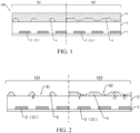
FIG. 1 is a schematic structural diagram of a display device before bending according toembodiment 1 of the present disclosure. -
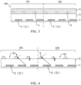
FIG. 2 is a schematic diagram of a first opening and a second opening according toembodiment 1 of the present disclosure. -
FIG. 3 is a schematic structural diagram of the display device before bending according toembodiment 2 of the present disclosure. -
FIG. 4 is a schematic diagram of the first opening and the second opening according toembodiment 2 of the present disclosure. -
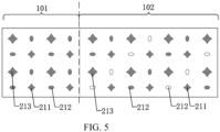
FIG. 5 is a schematic planar diagram of the display device according toembodiment 3 of the present disclosure. - Elements in the drawings are designated by reference numerals listed below:
- 100. display device; 101. planar display area;
- 102. non-planar display area;
- 1. substrate; 2. light-emitting layer;
- 3. encapsulation layer; 4. first optical film layer;
- 5. second optical film layer;
- 41. first opening; 42. second opening;
- 21. sub-pixel; 211. red sub-pixel;
- 212. green sub-pixel; and 213. blue sub-pixel.
- The preferred embodiments of the present disclosure are described in detail below with reference to the accompanying drawings. The specific embodiments described with reference to the attached drawings are all exemplary and are intended to illustrate and interpret the present disclosure to make the skilled in the art easier to understand how to implement the present disclosure. The disclosure herein provides many different embodiments or examples for realizing different structures of the present disclosure. They are only examples and are not intended to limit the present disclosure.
- In the description of the present disclosure, it should be understood that terms such as "upper", "lower", "front", "rear", "left", "right", "inside", "outside", "side", as well as derivative thereof should be construed to refer to the orientation as described or as shown in the drawings under discussion. These relative terms are for convenience of description, do not require that the present disclosure be constructed or operated in a particular orientation, and shall not be construed as causing limitations to the present disclosure.
- In the accompanying drawings, wherein the identical or similar reference numerals constantly denote the identical or similar elements or elements having the identical or similar functions. In the drawings, structurally identical components are denoted by the same reference numerals, and structural or functionally similar components are denoted by like reference numerals. Moreover, a size and a thickness of each component shown in the drawings are arbitrarily shown for ease of understanding and description, and the present disclosure does not limit the size and thickness of each component.
- As shown in
FIG. 1 , this embodiment provides adisplay device 100. Thedisplay device 100 includes aplanar display area 101 and anon-planar display area 102. - In this embodiment, the
display device 100 is a curved display device, and thenon-planar display area 102 is a curved display area. In other embodiments, thedisplay device 100 may also be a foldable display device, and thenon-planar display area 102 is a bending display area. - As shown in
FIG. 1 , thedisplay device 100 includes asubstrate 1, a light-emittinglayer 2, anencapsulation layer 3, a firstoptical film layer 4, and a secondoptical film layer 5. - Wherein, the
substrate 1 is located in theplanar display area 101 and thenon-planar display area 102. A material of thesubstrate 1 may be one or more of glass, polyimide, polycarbonate, polyethylene terephthalate, or polyethylene naphthalate. Therefore, thesubstrate 1 can have a better impact resistance, thereby effectively protecting thedisplay device 100. - The light-emitting
layer 2 is disposed on thesubstrate 1. The light-emittinglayer 2 includes a plurality of sub-pixels 21 arranged spaced apart from each other on thesubstrate 1. - The
encapsulation layer 3 is disposed on one side of the light-emittinglayer 2 away from thesubstrate 1. Theencapsulation layer 3 is mainly used to prevent water and oxygen from intruding the light-emittinglayer 2, thereby improving a service life of thedisplay device 100. Specifically, theencapsulation layer 3 may include a first inorganic layer, an organic layer, and a second inorganic layer. - As shown in
FIG. 1 , the firstoptical film layer 4 is disposed on one side of theencapsulation layer 3 away from thesubstrate 1. A refractive index of the firstoptical film layer 4 ranges from 1.3 to 1.6. In this embodiment, the refractive index of the firstoptical film layer 4 is 1.4. A material of the firstoptical film layer 4 may be an organic material such as acrylic or an epoxy resin, or may also be an inorganic material such as SiO2 or SiON. - As shown in
FIG. 1 , the secondoptical film layer 5 covers one side surface of the firstoptical film layer 4 away from thesubstrate 1. A refractive index of the secondoptical film layer 5 ranges from 1.5 to 1.9. The refractive index of the firstoptical film layer 4 is less than the refractive index of the secondoptical film layer 5. In this embodiment, the refractive index of the secondoptical film layer 5 is 1.7. A material of the secondoptical film layer 5 may be an organic material doped with nanoparticles such as ZrO2 or TiO2, or may also be an organic and inorganic hybrid material such as metal alkoxide. - As shown in
FIGs. 1 and 2 , the firstoptical film layer 4 is provided with at least onefirst opening 41 corresponding to a position of the sub-pixels 21 in theplanar display area 101. Wherein, the secondoptical film layer 5 is filled in thefirst opening 41. In this embodiment, the firstoptical film layer 4 is provided withfirst openings 41 corresponding to the sub-pixels 21 by one-to-one in theplanar display area 101. - In this embodiment, the
first openings 41 are through-holes penetrating through the firstoptical film layer 4, and a cross-sectional shape of thefirst openings 41 is inverted trapezoidal. One side surface of the firstoptical film layer 4 adjacent to thesubstrate 1 is parallel to one side surface of thesubstrate 1 adjacent to the firstoptical film layer 4. Therefore, an included angle between a tangent line of a side wall of thefirst openings 41 and thesubstrate 1 is equal to an included angle α between the side wall of thefirst openings 41 and the side surface of the firstoptical film layer 4 adjacent to thesubstrate 1. Wherein, the included angle α ranges from 65° to 75°. In this embodiment, the included angle α is 70°. - As shown in
FIGs. 1 and 2 , the firstoptical film layer 4 is provided with at least onesecond opening 42 corresponding to a position of the sub-pixels 21 in thenon-planar display area 102. Wherein, the secondoptical film layer 5 is filled in thesecond opening 42. - Wherein, in per unit area, a light-concentrating intensity of light emitted from the sub-pixels 21 in the
non-planar display area 102 and passing through the firstoptical film layer 4 and the secondoptical film layer 5 at a front viewing angle is less than a light-concentrating intensity of light emitted from the sub-pixels 21 in theplanar display area 101 and passing through the firstoptical film layer 4 and the secondoptical film layer 5 at the front viewing angle. Therefore, poor user experiences at a certain viewing angle in the non-planar display area in current technology can be improved, thereby improving user experiences. In practical applications, the light-concentrating intensities at the front viewing angle after the light passing through the first optical film layer and the second optical film layer may be detected under a same condition (for example, selecting light-emitting areas having a same unit area in the non-planar display area and the planar display area, emitting light under control of a same driving current, detecting at a position having a same distance to the non-planar display area and the planar display area, detecting at a same viewing angle, etc.). Based on this, a differentiated optical improvement effect of the first optical film layer and the second optical film layer between the non-planar display area and the planar display area can be judged. - In this embodiment, the first
optical film layer 4 is provided withsecond openings 42 corresponding to the sub-pixels 21 by one-to-one in thenon-planar display area 102. That is, in this embodiment, a density of thesecond openings 42 corresponding to the sub-pixels 21 in thenon-planar display area 102 is equal to a density of thefirst openings 41 corresponding to the sub-pixels 21 in theplanar display area 101. - In this embodiment, the
second openings 42 are grooves which do not penetrate through the firstoptical film layer 4, and a cross-sectional shape of thesecond openings 42 is arc. In this embodiment, in thenon-planar display area 102, a minimum thickness L1 of the firstoptical film layer 4 corresponding to thesecond openings 42 ranges from 10% to 30% of a maximum thickness L2 of the firstoptical film layer 4 which does not correspond to thesecond openings 42. Specifically, in thenon-planar display area 102, the minimum thickness L1 of the firstoptical film layer 4 corresponding to thesecond openings 42 ranges from 0.3 µm to 0.7 µm. The maximum thickness L2 of the firstoptical film layer 4 which does not correspond to thesecond openings 42 ranges from 1.5 µm to 2.5 µm. Therefore, stresses in thenon-planar display area 102 can be reduced, thereby reducing the stress concentration effect in thenon-planar display area 102 and preventing the firstoptical film layer 4 and the secondoptical film layer 5 from falling off or cracking. Further, the light-concentrating effect in thenon-planar display area 102 can also be reduced, so poor user experiences at a certain viewing angle in thenon-planar display area 102 in current technology can be improved, thereby improving user experiences. - As shown in
FIGs. 1 and 2 , the side surface of the firstoptical film layer 4 adjacent to thesubstrate 1 is parallel to the side surface of thesubstrate 1 adjacent to the firstoptical film layer 4. Therefore, an included angle between a tangent line of a side wall of thesecond openings 42 and thesubstrate 1 is equal to an included angle γ between the side wall of thesecond openings 42 and the side surface of the firstoptical film layer 4 adjacent to thesubstrate 1. Wherein, the included angle γ ranges from 20° to 50°. In this embodiment, the included angle γ is 35°. - As shown in
FIG. 2 , the included angle γ is smaller than the included angle α, that is, the included angle γ is slightly gentler than the included angle α, and a light-concentrating effect of thesecond openings 42 and the secondoptical film layer 5 in thenon-planar display area 102 is slightly lower than that of thefirst openings 41 and the secondoptical film layer 5 in theplanar display area 101. Therefore, poor user experiences at the certain viewing angle in thenon-planar display area 102 in current technology can be improved, thereby improving user experiences. - As shown in
FIG. 2 , the included angle γ is smaller than the included angle α, that is, the included angle γ is slightly gentler than the included angle α, that is, a sudden change in a shape of thesecond openings 42 in thenon-planar display area 102 can be reduced. Therefore, stresses in thenon-planar display area 102 can be reduced, thereby reducing the stress concentration effect in thenon-planar display area 102 and preventing the firstoptical film layer 4 and the secondoptical film layer 5 from falling off or cracking. - As shown in
FIG. 3 , this embodiment provides adisplay device 100. Thedisplay device 100 includes aplanar display area 101 and anon-planar display area 102. - In this embodiment, the
display device 100 is a curved display device, and thenon-planar display area 102 is a curved display area. In other embodiments, thedisplay device 100 may also be a foldable display device, and thenon-planar display area 102 is a bending display area. - As shown in
FIG. 3 , thedisplay device 100 includes asubstrate 1, a light-emittinglayer 2, anencapsulation layer 3, a firstoptical film layer 4, and a secondoptical film layer 5. - Wherein, the
substrate 1 is located in theplanar display area 101 and thenon-planar display area 102. A material of thesubstrate 1 may be one or more of glass, polyimide, polycarbonate, polyethylene terephthalate, or polyethylene naphthalate. Therefore, thesubstrate 1 can have a better impact resistance, thereby effectively protecting thedisplay device 100. - The light-emitting
layer 2 is disposed on thesubstrate 1. The light-emittinglayer 2 includes a plurality of sub-pixels 21 arranged spaced apart from each other on thesubstrate 1. - The
encapsulation layer 3 is disposed on one side of the light-emittinglayer 2 away from thesubstrate 1. Theencapsulation layer 3 is mainly used to prevent water and oxygen from intruding the light-emittinglayer 2, thereby improving a service life of thedisplay device 100. Specifically, theencapsulation layer 3 may include a first inorganic layer, an organic layer, and a second inorganic layer. - As shown in
FIG. 1 , the firstoptical film layer 4 is disposed on one side of theencapsulation layer 3 away from thesubstrate 1. A refractive index of the firstoptical film layer 4 ranges from 1.3 to 1.6. In this embodiment, the refractive index of the firstoptical film layer 4 is 1.4. A material of the firstoptical film layer 4 may be an organic material such as acrylic or an epoxy resin, or may also be an inorganic material such as SiO2 or SiON. - As shown in
FIG. 1 , the secondoptical film layer 5 covers one side surface of the firstoptical film layer 4 away from thesubstrate 1. A refractive index of the secondoptical film layer 5 ranges from 1.5 to 1.9. The refractive index of the firstoptical film layer 4 is less than the refractive index of the secondoptical film layer 5. In this embodiment, the refractive index of the secondoptical film layer 5 is 1.7. A material of the secondoptical film layer 5 may be an organic material doped with nanoparticles such as ZrO2 or TiO2, or may also be an organic and inorganic hybrid material such as metal alkoxide. - As shown in
FIGs. 3 and 4 , the firstoptical film layer 4 is provided with at least onefirst opening 41 corresponding to a position of the sub-pixels 21 in theplanar display area 101. Wherein, the secondoptical film layer 5 is filled in thefirst opening 41. In this embodiment, the firstoptical film layer 4 is provided withfirst openings 41 corresponding to the sub-pixels 21 by one-to-one in theplanar display area 101. - In this embodiment, the
first openings 41 are through-holes penetrating through the firstoptical film layer 4, and a cross-sectional shape of thefirst openings 41 is inverted trapezoidal. One side surface of the firstoptical film layer 4 adjacent to thesubstrate 1 is parallel to one side surface of thesubstrate 1 adjacent to the firstoptical film layer 4. Therefore, an included angle between a tangent line of a side wall of thefirst openings 41 and thesubstrate 1 is equal to an included angle α between the side wall of thefirst openings 41 and the side surface of the firstoptical film layer 4 adjacent to thesubstrate 1. Wherein, the included angle α ranges from 65° to 75°. In this embodiment, the included angle α is 70°. - As shown in
FIGs. 3 and 4 , the firstoptical film layer 4 is provided with at least onesecond opening 42 corresponding to a position of the sub-pixels 21 in thenon-planar display area 102. - Wherein, in per unit area, a light-concentrating intensity of light emitted from the sub-pixels 21 in the
non-planar display area 102 and passing through the firstoptical film layer 4 and the secondoptical film layer 5 at a front viewing angle is less than a light-concentrating intensity of light emitted from the sub-pixels 21 in theplanar display area 101 and passing through the firstoptical film layer 4 and the secondoptical film layer 5 at the front viewing angle. Therefore, poor user experiences at a certain viewing angle in the non-planar display area in current technology can be improved, thereby improving user experiences. - In this embodiment, the first
optical film layer 4 is provided withsecond openings 42 corresponding to the sub-pixels 21 by one-to-one in thenon-planar display area 102. That is, in this embodiment, a density of thesecond openings 42 corresponding to the sub-pixels 21 in thenon-planar display area 102 is equal to a density of thefirst openings 41 corresponding to the sub-pixels 21 in theplanar display area 101. - In this embodiment, the
second openings 42 are through-holes penetrating through the firstoptical film layer 4, and a cross-sectional shape of thesecond openings 42 is inverted trapezoidal. One side surface of the firstoptical film layer 4 adjacent to thesubstrate 1 is parallel to one side surface of thesubstrate 1 adjacent to the firstoptical film layer 4. Therefore, an included angle between a tangent line of a side wall of thesecond openings 42 and thesubstrate 1 is equal to an included angle β between the side wall of thesecond openings 42 and the side surface of the firstoptical film layer 4 adjacent to thesubstrate 1. Wherein, the included angle β ranges from 20° to 50°. In this embodiment, the included angle β is 35°. - As shown in
FIG. 4 , the included angle β is smaller than the included angle α, that is, the included angle β is slightly gentler than the included angle α, so when light with a same incident angle irradiates on the side walls of thefirst openings 41 and thesecond openings 42 and is reflected, a light-concentrating effect of thesecond openings 42 and the secondoptical film layer 5 in thenon-planar display area 102 is slightly lower than that of thefirst openings 41 and the secondoptical film layer 5 in theplanar display area 101. Therefore, poor user experiences at the certain viewing angle in thenon-planar display area 102 in current technology can be improved, thereby improving user experiences. - As shown in
FIG. 4 , the included angle β is smaller than the included angle α, that is, the included angle β is slightly gentler than the included angle α, that is, a sudden change in a shape of thesecond openings 42 in thenon-planar display area 102 can be reduced. Therefore, stresses in thenon-planar display area 102 can be reduced, thereby reducing the stress concentration effect in thenon-planar display area 102 and preventing the firstoptical film layer 4 and the secondoptical film layer 5 from falling off or cracking. - As shown in
FIG. 5 , this embodiment includes most technical features ofembodiments embodiments second openings 42 corresponding to the sub-pixels 21 in thenon-planar display area 102 is less than the density of thefirst openings 41 corresponding to the sub-pixels 21 in theplanar display area 101. - As shown in
FIG. 5 , the sub-pixels 21 includered sub-pixels 211,green sub-pixels 212, andblue sub-pixels 213. Wherein, the sub-pixels 21 filled with shadows in theplanar display area 101 mean that the firstoptical film layer 4 corresponding to the sub-pixels 21 is provided with thefirst openings 41. The sub-pixels 21 filled with shadows in thenon-planar display area 102 mean that the firstoptical film layer 4 corresponding to the sub-pixels 21 is provided with thesecond openings 42, and the sub-pixels 21 that are not filled with shadows in thenon-planar display area 102 mean that the firstoptical film layer 4 corresponding to the sub-pixels 21 is not provided with thesecond openings 42. - A luminous efficiency of the
green sub-pixels 212 is higher than luminous efficiencies of thered sub-pixels 211 and theblue sub-pixels 213, so in this embodiment, the density of thesecond openings 42 corresponding to thegreen sub-pixels 212 in thenon-planar display area 102 is reduced. Specifically, the density of thesecond openings 42 corresponding to thegreen sub-pixels 212 in thenon-planar display area 102 ranges from 0% to 75% of the density of thefirst openings 41 corresponding to thegreen sub-pixels 212 in theplanar display area 101. - Therefore, stresses in the
non-planar display area 102 can be reduced by reducing the density of thesecond openings 42 corresponding to the sub-pixels 21 in thenon-planar display area 102, thereby reducing the stress concentration effect in thenon-planar display area 102 and preventing the firstoptical film layer 4 and the secondoptical film layer 5 from falling off or cracking. - The display device provided in the embodiments of the present disclosure is described in detail above. Specific examples are used herein to explain the principles and implementation of the present disclosure. The descriptions of the above embodiments are only used to help understand the method of the present disclosure and its core ideas; meanwhile, for those skilled in the art, the range of specific implementation and application may be changed according to the ideas of the present disclosure. In summary, the content of the specification should not be construed as causing limitations to the present disclosure.
Claims (10)
- A display device, having a planar display area and a non-planar display area and comprising:a substrate;a light-emitting layer disposed on one side of the substrate and comprising a plurality of sub-pixels arranged spaced apart from each other;a first optical film layer disposed on one side of the light-emitting layer away from the substrate, wherein the first optical film layer is provided with at least one first opening corresponding to a position of the sub-pixels in the planar display area, and the first optical film layer is provided with at least one second opening corresponding to a position of the sub-pixels in the non-planar display area; anda second optical film layer covering one side of the first optical film layer away from the substrate and filled in the first opening and the second opening, wherein a refractive index of the first optical film layer is less than a refractive index of the second optical film layer;wherein in per unit area, a light-concentrating intensity of light emitted from the sub-pixels in the non-planar display area and passing through the first optical film layer and the second optical film layer at a front viewing angle is less than a light-concentrating intensity of light emitted from the sub-pixels in the planar display area and passing through the first optical film layer and the second optical film layer at the front viewing angle.
- The display device according to claim 1, wherein in a cross-section perpendicular to the substrate, an included angle between a tangent line of a side wall of the second opening and the substrate is less than an included angle between a tangent line of a side wall of the first opening and the substrate.
- The display device according to claim 2, wherein in the non-planar display area, a minimum thickness of the first optical film layer corresponding to the second opening ranges from 10% to 30% of a maximum thickness of the first optical film layer not corresponding to the second opening.
- The display device according to claim 3, wherein in the non-planar display area, the minimum thickness of the first optical film layer corresponding to the second opening ranges from 0.3 µm to 0.7 µm, and the maximum thickness of the first optical film layer not corresponding to the second opening ranges from 1.5 µm to 2.5 µm.
- The display device according to claim 3, wherein the second opening is a groove which does not penetrate through the first optical film layer, and a cross-sectional shape of the second opening is arc; and
the first opening penetrates through the first optical film layer. - The display device according to claim 2, wherein the included angle between the tangent line of the side wall of the second opening and the substrate ranges from 20° to 50°.
- The display device according to claim 6, wherein the first opening and the second opening both penetrate through the first optical film layer; and
cross-sectional shapes of the first opening and the second opening are inverted trapezoidal, and the included angle between the tangent line of the side wall of the first opening and the substrate ranges from 65° to 75°. - The display device according to claim 2, wherein a density of the second opening in the non-planar display area is less than or equal to a density of the first opening in the planar display area.
- The display device according to claim 8, wherein the sub-pixels comprise red sub-pixels, green sub-pixels, and blue sub-pixels; and
the density of the second opening corresponding to the green sub-pixels in the non-planar display area ranges from 0% to 75% of the density of the first opening corresponding to the green sub-pixels in the planar display area. - The display device according to claim 1, wherein the refractive index of the first optical film layer ranges from 1.3 to 1.6, and the refractive index of the second optical film layer ranges from 1.5 to 1.9.
Applications Claiming Priority (2)
| Application Number | Priority Date | Filing Date | Title |
|---|---|---|---|
| CN202210193616.XA CN114597324B (en) | 2022-03-01 | 2022-03-01 | Display device |
| PCT/CN2022/079997 WO2023164960A1 (en) | 2022-03-01 | 2022-03-09 | Display device |
Publications (2)
| Publication Number | Publication Date |
|---|---|
| EP4489053A1 true EP4489053A1 (en) | 2025-01-08 |
| EP4489053A4 EP4489053A4 (en) | 2026-01-14 |
Family
ID=81808304
Family Applications (1)
| Application Number | Title | Priority Date | Filing Date |
|---|---|---|---|
| EP22757816.8A Pending EP4489053A4 (en) | 2022-03-01 | 2022-03-09 | DISPLAY DEVICE |
Country Status (6)
| Country | Link |
|---|---|
| US (1) | US12336419B2 (en) |
| EP (1) | EP4489053A4 (en) |
| JP (1) | JP7560565B2 (en) |
| KR (1) | KR102746189B1 (en) |
| CN (1) | CN114597324B (en) |
| WO (1) | WO2023164960A1 (en) |
Families Citing this family (2)
| Publication number | Priority date | Publication date | Assignee | Title |
|---|---|---|---|---|
| WO2022249447A1 (en) * | 2021-05-28 | 2022-12-01 | シャープディスプレイテクノロジー株式会社 | Display device and method for manufacturing display device |
| US20260098292A1 (en) | 2022-09-30 | 2026-04-09 | Optolane Technologies Inc. | Digital real-time pcr analysis method |
Family Cites Families (24)
| Publication number | Priority date | Publication date | Assignee | Title |
|---|---|---|---|---|
| JP2012059692A (en) * | 2010-08-09 | 2012-03-22 | Canon Inc | Organic electroluminescent display device |
| KR101855977B1 (en) * | 2016-06-27 | 2018-05-09 | 주식회사 제이에이치이엔지 | Form for construction structure |
| KR102367247B1 (en) * | 2017-07-04 | 2022-02-25 | 삼성디스플레이 주식회사 | Display device |
| US11963425B1 (en) * | 2018-07-10 | 2024-04-16 | Apple Inc. | Electronic devices having displays with curved surfaces |
| KR102631253B1 (en) * | 2018-11-05 | 2024-01-31 | 삼성디스플레이 주식회사 | flexible display device |
| KR102691390B1 (en) * | 2018-11-28 | 2024-08-01 | 엘지디스플레이 주식회사 | Organic light emitting diodes display |
| KR102748010B1 (en) * | 2019-01-24 | 2024-12-30 | 삼성디스플레이 주식회사 | Display device |
| CN110164938B (en) * | 2019-05-30 | 2021-07-30 | 武汉天马微电子有限公司 | Display panel and display device |
| KR102818425B1 (en) | 2019-08-30 | 2025-06-10 | 엘지디스플레이 주식회사 | Light emitting display apparatus |
| CN111341808B (en) * | 2020-03-05 | 2023-01-17 | 京东方科技集团股份有限公司 | A display substrate and its preparation method, visible light communication device |
| CN111446276A (en) * | 2020-03-31 | 2020-07-24 | 武汉天马微电子有限公司 | Display panel and display device |
| CN111508343B (en) * | 2020-05-29 | 2022-03-18 | 武汉天马微电子有限公司 | A display panel and display device |
| CN111755492A (en) | 2020-06-24 | 2020-10-09 | 武汉华星光电半导体显示技术有限公司 | Display panel and display device |
| CN115295744B (en) * | 2020-06-28 | 2025-09-19 | 湖北长江新型显示产业创新中心有限公司 | Display panel and display device |
| CN112038370B (en) * | 2020-08-20 | 2022-07-12 | 武汉华星光电半导体显示技术有限公司 | Curved screen and method for manufacturing curved screen |
| CN112086578B (en) | 2020-09-14 | 2022-05-31 | 武汉华星光电半导体显示技术有限公司 | Display panel and display device |
| CN112420783B (en) | 2020-11-04 | 2022-09-09 | 武汉华星光电半导体显示技术有限公司 | Display panel and electronic device |
| CN113394351B (en) * | 2021-06-11 | 2022-08-09 | 武汉天马微电子有限公司 | Display panel and display device |
| CN215299293U (en) * | 2021-06-24 | 2021-12-24 | 昆山国显光电有限公司 | Display panel |
| KR20230033189A (en) * | 2021-08-30 | 2023-03-08 | 삼성디스플레이 주식회사 | Display device and manufacturing method for the same |
| CN113745298B (en) * | 2021-08-31 | 2022-09-09 | 武汉华星光电半导体显示技术有限公司 | a display panel |
| CN114023908B (en) | 2021-11-03 | 2024-02-02 | 云谷(固安)科技有限公司 | Display panel, preparation method and display device thereof |
| CN114050224B (en) * | 2021-11-29 | 2023-07-07 | 合肥维信诺科技有限公司 | Display panel and display device |
| CN114613813B (en) * | 2022-02-25 | 2023-08-25 | 武汉华星光电半导体显示技术有限公司 | Display device |
-
2022
- 2022-03-01 CN CN202210193616.XA patent/CN114597324B/en active Active
- 2022-03-09 KR KR1020227023602A patent/KR102746189B1/en active Active
- 2022-03-09 WO PCT/CN2022/079997 patent/WO2023164960A1/en not_active Ceased
- 2022-03-09 EP EP22757816.8A patent/EP4489053A4/en active Pending
- 2022-03-09 JP JP2022552426A patent/JP7560565B2/en active Active
- 2022-03-09 US US17/754,243 patent/US12336419B2/en active Active
Also Published As
| Publication number | Publication date |
|---|---|
| US20240057456A1 (en) | 2024-02-15 |
| WO2023164960A1 (en) | 2023-09-07 |
| KR102746189B1 (en) | 2024-12-26 |
| US12336419B2 (en) | 2025-06-17 |
| EP4489053A4 (en) | 2026-01-14 |
| JP7560565B2 (en) | 2024-10-02 |
| CN114597324B (en) | 2023-05-12 |
| KR20230130522A (en) | 2023-09-12 |
| JP2024510857A (en) | 2024-03-12 |
| CN114597324A (en) | 2022-06-07 |
Similar Documents
| Publication | Publication Date | Title |
|---|---|---|
| CN109671864B (en) | OLED display panel | |
| WO2021120314A1 (en) | Display panel | |
| EP3190623B1 (en) | Organic light-emitting diode display panel, manufacturing method therefor, and display apparatus | |
| US9281501B2 (en) | Light extraction film and light emitting device using the same | |
| US12336419B2 (en) | Display device | |
| CN102664239A (en) | organic electroluminescent device | |
| JP5523870B2 (en) | Surface light emitting device | |
| KR102345872B1 (en) | Organic light emitting display device and method of manufacturing the same | |
| US20070278951A1 (en) | Backlight unit and liquid crystal display device including the same | |
| US10367170B2 (en) | Light emitting device with irregularities located on a first light transmissive substrate and a second light transmissive substrate | |
| KR20250021526A (en) | Light emitting display device | |
| CN114613813B (en) | Display device | |
| WO2021027141A1 (en) | Display panel | |
| US11991915B2 (en) | Display panel and display device | |
| KR102867757B1 (en) | display device | |
| CN114023902B (en) | Display panel | |
| WO2015181869A1 (en) | Light emitting device | |
| CN114566601A (en) | Display panel and preparation method thereof | |
| CN114520300A (en) | Display panel and display device | |
| KR20150009734A (en) | Oled | |
| US20240049549A1 (en) | Display panel | |
| CN114361216B (en) | Display panel | |
| CN210182417U (en) | Low-power consumption organic light-emitting diode display screen | |
| KR102834122B1 (en) | Light emitting display apparatus | |
| CN113555515A (en) | Light-emitting device and display panel |
Legal Events
| Date | Code | Title | Description |
|---|---|---|---|
| STAA | Information on the status of an ep patent application or granted ep patent |
Free format text: STATUS: UNKNOWN |
|
| STAA | Information on the status of an ep patent application or granted ep patent |
Free format text: STATUS: THE INTERNATIONAL PUBLICATION HAS BEEN MADE |
|
| PUAI | Public reference made under article 153(3) epc to a published international application that has entered the european phase |
Free format text: ORIGINAL CODE: 0009012 |
|
| STAA | Information on the status of an ep patent application or granted ep patent |
Free format text: STATUS: REQUEST FOR EXAMINATION WAS MADE |
|
| 17P | Request for examination filed |
Effective date: 20220831 |
|
| AK | Designated contracting states |
Kind code of ref document: A1 Designated state(s): AL AT BE BG CH CY CZ DE DK EE ES FI FR GB GR HR HU IE IS IT LI LT LU LV MC MK MT NL NO PL PT RO RS SE SI SK SM TR |
|
| DAV | Request for validation of the european patent (deleted) | ||
| DAX | Request for extension of the european patent (deleted) | ||
| REG | Reference to a national code |
Ref country code: DE Ref legal event code: R079 Free format text: PREVIOUS MAIN CLASS: H99Z9999999999 Ipc: H10K0059800000 |
|
| A4 | Supplementary search report drawn up and despatched |
Effective date: 20251217 |
|
| RIC1 | Information provided on ipc code assigned before grant |
Ipc: H10K 59/80 20230101AFI20251211BHEP Ipc: H10K 59/35 20230101ALI20251211BHEP Ipc: H10K 77/10 20230101ALN20251211BHEP Ipc: H10K 102/00 20230101ALN20251211BHEP |