EP4485504A1 - Front side ohmic contact formation for sic device - Google Patents
Front side ohmic contact formation for sic device Download PDFInfo
- Publication number
- EP4485504A1 EP4485504A1 EP24180124.0A EP24180124A EP4485504A1 EP 4485504 A1 EP4485504 A1 EP 4485504A1 EP 24180124 A EP24180124 A EP 24180124A EP 4485504 A1 EP4485504 A1 EP 4485504A1
- Authority
- EP
- European Patent Office
- Prior art keywords
- metallic layer
- layer
- base material
- semiconductor base
- metallic
- Prior art date
- Legal status (The legal status is an assumption and is not a legal conclusion. Google has not performed a legal analysis and makes no representation as to the accuracy of the status listed.)
- Pending
Links
Images




Classifications
-
- H—ELECTRICITY
- H10—SEMICONDUCTOR DEVICES; ELECTRIC SOLID-STATE DEVICES NOT OTHERWISE PROVIDED FOR
- H10P—GENERIC PROCESSES OR APPARATUS FOR THE MANUFACTURE OR TREATMENT OF DEVICES COVERED BY CLASS H10
- H10P14/00—Formation of materials, e.g. in the shape of layers or pillars
- H10P14/40—Formation of materials, e.g. in the shape of layers or pillars of conductive or resistive materials
-
- H—ELECTRICITY
- H10—SEMICONDUCTOR DEVICES; ELECTRIC SOLID-STATE DEVICES NOT OTHERWISE PROVIDED FOR
- H10D—INORGANIC ELECTRIC SEMICONDUCTOR DEVICES
- H10D64/00—Electrodes of devices having potential barriers
- H10D64/01—Manufacture or treatment
- H10D64/011—Manufacture or treatment of electrodes ohmically coupled to a semiconductor
- H10D64/0111—Manufacture or treatment of electrodes ohmically coupled to a semiconductor to Group IV semiconductors
- H10D64/0115—Manufacture or treatment of electrodes ohmically coupled to a semiconductor to Group IV semiconductors to silicon carbide
-
- H—ELECTRICITY
- H10—SEMICONDUCTOR DEVICES; ELECTRIC SOLID-STATE DEVICES NOT OTHERWISE PROVIDED FOR
- H10D—INORGANIC ELECTRIC SEMICONDUCTOR DEVICES
- H10D62/00—Semiconductor bodies, or regions thereof, of devices having potential barriers
- H10D62/80—Semiconductor bodies, or regions thereof, of devices having potential barriers characterised by the materials
- H10D62/83—Semiconductor bodies, or regions thereof, of devices having potential barriers characterised by the materials being Group IV materials, e.g. B-doped Si or undoped Ge
- H10D62/832—Semiconductor bodies, or regions thereof, of devices having potential barriers characterised by the materials being Group IV materials, e.g. B-doped Si or undoped Ge being Group IV materials comprising two or more elements, e.g. SiGe
- H10D62/8325—Silicon carbide
-
- H—ELECTRICITY
- H10—SEMICONDUCTOR DEVICES; ELECTRIC SOLID-STATE DEVICES NOT OTHERWISE PROVIDED FOR
- H10D—INORGANIC ELECTRIC SEMICONDUCTOR DEVICES
- H10D62/00—Semiconductor bodies, or regions thereof, of devices having potential barriers
- H10D62/10—Shapes, relative sizes or dispositions of the regions of the semiconductor bodies; Shapes of the semiconductor bodies
- H10D62/102—Constructional design considerations for preventing surface leakage or controlling electric field concentration
- H10D62/103—Constructional design considerations for preventing surface leakage or controlling electric field concentration for increasing or controlling the breakdown voltage of reverse-biased devices
- H10D62/105—Constructional design considerations for preventing surface leakage or controlling electric field concentration for increasing or controlling the breakdown voltage of reverse-biased devices by having particular doping profiles, shapes or arrangements of PN junctions; by having supplementary regions, e.g. junction termination extension [JTE]
- H10D62/106—Constructional design considerations for preventing surface leakage or controlling electric field concentration for increasing or controlling the breakdown voltage of reverse-biased devices by having particular doping profiles, shapes or arrangements of PN junctions; by having supplementary regions, e.g. junction termination extension [JTE] having supplementary regions doped oppositely to or in rectifying contact with regions of the semiconductor bodies, e.g. guard rings with PN or Schottky junctions
-
- H—ELECTRICITY
- H10—SEMICONDUCTOR DEVICES; ELECTRIC SOLID-STATE DEVICES NOT OTHERWISE PROVIDED FOR
- H10D—INORGANIC ELECTRIC SEMICONDUCTOR DEVICES
- H10D64/00—Electrodes of devices having potential barriers
- H10D64/01—Manufacture or treatment
-
- H—ELECTRICITY
- H10—SEMICONDUCTOR DEVICES; ELECTRIC SOLID-STATE DEVICES NOT OTHERWISE PROVIDED FOR
- H10D—INORGANIC ELECTRIC SEMICONDUCTOR DEVICES
- H10D64/00—Electrodes of devices having potential barriers
- H10D64/01—Manufacture or treatment
- H10D64/012—Manufacture or treatment of electrodes comprising a Schottky barrier to a semiconductor
- H10D64/0121—Manufacture or treatment of electrodes comprising a Schottky barrier to a semiconductor to Group IV semiconductors
- H10D64/0123—Manufacture or treatment of electrodes comprising a Schottky barrier to a semiconductor to Group IV semiconductors to silicon carbide
-
- H—ELECTRICITY
- H10—SEMICONDUCTOR DEVICES; ELECTRIC SOLID-STATE DEVICES NOT OTHERWISE PROVIDED FOR
- H10D—INORGANIC ELECTRIC SEMICONDUCTOR DEVICES
- H10D64/00—Electrodes of devices having potential barriers
- H10D64/20—Electrodes characterised by their shapes, relative sizes or dispositions
- H10D64/23—Electrodes carrying the current to be rectified, amplified, oscillated or switched, e.g. sources, drains, anodes or cathodes
-
- H—ELECTRICITY
- H10—SEMICONDUCTOR DEVICES; ELECTRIC SOLID-STATE DEVICES NOT OTHERWISE PROVIDED FOR
- H10D—INORGANIC ELECTRIC SEMICONDUCTOR DEVICES
- H10D64/00—Electrodes of devices having potential barriers
- H10D64/60—Electrodes characterised by their materials
- H10D64/62—Electrodes ohmically coupled to a semiconductor
-
- H—ELECTRICITY
- H10—SEMICONDUCTOR DEVICES; ELECTRIC SOLID-STATE DEVICES NOT OTHERWISE PROVIDED FOR
- H10D—INORGANIC ELECTRIC SEMICONDUCTOR DEVICES
- H10D64/00—Electrodes of devices having potential barriers
- H10D64/60—Electrodes characterised by their materials
- H10D64/64—Electrodes comprising a Schottky barrier to a semiconductor
-
- H—ELECTRICITY
- H10—SEMICONDUCTOR DEVICES; ELECTRIC SOLID-STATE DEVICES NOT OTHERWISE PROVIDED FOR
- H10D—INORGANIC ELECTRIC SEMICONDUCTOR DEVICES
- H10D8/00—Diodes
- H10D8/01—Manufacture or treatment
- H10D8/051—Manufacture or treatment of Schottky diodes
-
- H—ELECTRICITY
- H10—SEMICONDUCTOR DEVICES; ELECTRIC SOLID-STATE DEVICES NOT OTHERWISE PROVIDED FOR
- H10D—INORGANIC ELECTRIC SEMICONDUCTOR DEVICES
- H10D8/00—Diodes
- H10D8/60—Schottky-barrier diodes
-
- H—ELECTRICITY
- H10—SEMICONDUCTOR DEVICES; ELECTRIC SOLID-STATE DEVICES NOT OTHERWISE PROVIDED FOR
- H10P—GENERIC PROCESSES OR APPARATUS FOR THE MANUFACTURE OR TREATMENT OF DEVICES COVERED BY CLASS H10
- H10P34/00—Irradiation with electromagnetic or particle radiation of wafers, substrates or parts of devices
- H10P34/40—Irradiation with electromagnetic or particle radiation of wafers, substrates or parts of devices with high-energy radiation
- H10P34/42—Irradiation with electromagnetic or particle radiation of wafers, substrates or parts of devices with high-energy radiation with electromagnetic radiation, e.g. laser annealing
-
- H—ELECTRICITY
- H10—SEMICONDUCTOR DEVICES; ELECTRIC SOLID-STATE DEVICES NOT OTHERWISE PROVIDED FOR
- H10D—INORGANIC ELECTRIC SEMICONDUCTOR DEVICES
- H10D64/00—Electrodes of devices having potential barriers
- H10D64/111—Field plates
Definitions
- the present invention relates to the field of silicon carbide (SiC) power devices, and in particular, to front side ohmic contact formations for SiC power devices.
- SiC silicon carbide
- Applicant has identified many technical challenges and difficulties associated with SiC devices, such as the SiC power devices, in particular problems related to the fabrication of SiC power devices.
- An ohmic contact formation may require a (i) metal deposition, such as a nickel or other conductive material, (ii) an annealing temperature at near 1000°C to trigger a reaction between the metal deposition and the SiC (e.g., to form of silicides, titanium silicides, etc.), and (iii) the removal of portions of the metal deposition that are in direct contact with the SiC surface.
- the selective removal of portions of the metal deposition may be complex and, in part due to the complexity, is unreliable and prone to errors, while being critical to the functionality of SiC devices.
- traditional techniques for fabricating SiC devices face technical challenges that decrease their reliability, while increasing the rate of failure as well as the cost and expense of fabrication.
- an aim of the present invention is to overcome the disadvantages of the prior art.
- a method in particular a method for fabricating a SiC device, and a SiC device are provided, as defined in the appended claims.
- a method includes providing a semiconductor base material comprising a first side and a second side, wherein the semiconductor base material comprises a silicon carbide (SiC) material; forming a first metallic layer on a first side of the semiconductor base material to form a Schottky contact; forming a second metallic layer over the first metallic layer to form a reflective barrier layer covering the Schottky contact; removing one or more portions of the second metallic layer to expose a first portion of the first metallic layer; and forming, through a laser annealing process, one or more silicide portions on the first metallic layer to form one or more ohmic contacts within the Schottky contact.
- SiC silicon carbide
- the first metallic layer forms the one or more ohmic contacts and the Schottky contact within a p+ region.
- the method further includes, subsequent to forming the one or more silicide portions on the first metallic layer, forming a dielectric layer on the first side of the semiconductor base material.
- the dielectric layer may cover the semiconductor base material, the first metallic layer, and the second metallic layer.
- the method includes placing a dielectric layer mask over one or more peripheral dielectric portions of the dielectric layer; etching an interior dielectric portion from the dielectric layer to expose the second metallic layer and the one or more silicide portions on the first metallic layer; and removing the dielectric layer mask.
- the method includes forming a frontside metallic layer over the first side of the semiconductor base material, the dielectric layer, the first metallic layer, and the second metallic layer; placing a frontside metallic layer mask over an interior portion of the frontside metallic layer; etching a peripheral frontside metallic portion from the frontside metallic layer to expose the dielectric layer; and removing the frontside metallic layer mask.
- the method includes forming a passivation layer over the dielectric layer and the frontside metallic layer; placing a passivation layer mask over a peripheral portion of the passivation layer; etching an interior passivation layer portion from the passivation layer to expose the frontside metallic layer; and removing the passivation layer mask.
- removing the one or more portions of the second metallic layer includes placing a patterned mask over the second metallic layer.
- the patterned mask may expose the one or more portions of the second metallic layer.
- the method may include etching the second metallic layer, through the patterned mask, to remove the one or more portions of the second metallic layer; and removing the patterned mask.
- the method includes, subsequent to forming the one or more silicide portions on the first metallic layer, removing one or more peripheral portions of the first metallic layer and the second metallic layer to expose at least a portion of the semiconductor base material.
- removing the one or more peripheral portions of the first metallic layer includes placing an interior mask over the second metallic layer, wherein the interior mask exposes the one or more peripheral portions of the second metallic layer; etching the second metallic layer and the first metallic layer, around the interior mask, to remove the one or more peripheral portions of the second metallic layer and the first metallic layer; and removing the interior mask.
- the semiconductor base material includes one or more anode implants and the one or more silicide portions on the first metallic layer correspond to the one or more anode implants.
- the method includes forming the one or more anode implants within the first side of the semiconductor base material.
- the first side of the semiconductor base material includes an epitaxial drift layer and the second side of the semiconductor base material includes a doped SiC substrate.
- the method includes forming a backside ohmic contact on the second side of the semiconductor base material; and forming a backside metallic layer over the backside ohmic contact.
- the first metallic layer includes a nickel-based material.
- the second metallic layer includes an aluminum-based material.
- a silicon carbide (SiC) power device includes a semiconductor base material with a first side and a second side; a first metallic layer disposed on the first side of the semiconductor base material, wherein a first portion of the first metallic layer forms one or more ohmic contacts and a second portion of the first metallic layer forms a Schottky contact; and a second metallic layer disposed on the second portion of the first metallic layer.
- SiC silicon carbide
- the first side of the semiconductor base material includes an epitaxial drift layer.
- the second side of the semiconductor base material includes a doped SiC substrate.
- the first metallic layer includes a nickel material.
- the second metallic layer includes an aluminum material.
- Various example embodiments of the present disclosure are directed to improved SiC devices and systems, apparatuses, products, and methods for fabricating improved SiC devices.
- the present disclosure in some examples, describes a method for the realization of front side ohmic contacts for SiC Merged PiN Schottky (MPS) devices, among other SiC devices, that improve upon traditional techniques for fabricating SiC devices.
- MPS SiC Merged PiN Schottky
- some embodiments of the present disclosure provide an improved SiC formation that includes a single layer of metal to realize both a Schottky contact and ohmic contact.
- the Schottky contact and the Ohmic contact may be realized through a laser annealing process by shielding the single layer of metal by a patterned second metal layer.
- Each layer may not be sacrificial and may be part of an active area of the SiC device; thereby reducing the risk of damaging the SiC device by removing metal layers in direct contact with a SiC surface.
- the fabricating process includes providing a semiconductor base material with a first side and a second side, forming a first metallic layer on a first side of the semiconductor base material to form a Schottky contact, forming a second metallic layer over the first metallic layer to form a reflective barrier layer covering the Schottky contact, removing one or more portions of the second metallic layer to expose a first portion of the first metallic layer; and forming, through a laser annealing process, one or more silicide portions (e.g., titanium silicides, etc.) on the first metallic layer to form one or more ohmic contacts within the Schottky contact.
- silicide portions e.g., titanium silicides, etc.
- FIG. 1 illustrates an example computing system 100 in accordance with one or more embodiments of the present disclosure.
- the terms computing system, computer, system, device, entity, and/or similar words used herein interchangeably may refer to, for example, one or more computers, computing entities, desktops, mobile phones, tablets, notebooks, laptops, distributed systems, kiosks, input terminals, servers or server networks, blades, gateways, switches, processing devices, processing entities, set-top boxes, relays, routers, network access points, base stations, the like, and/or any combination of devices or entities adapted to perform the functions, operations, and/or processes described herein.
- Such functions, operations, and/or processes may include, for example, transmitting, receiving, operating on, processing, displaying, storing, determining, creating/generating, monitoring, evaluating, comparing, and/or similar terms used herein interchangeably. In one embodiment, these functions, operations, and/or processes may be performed on data, content, information, and/or similar terms used herein interchangeably.
- the computing system 100 may include a computing apparatus 110 and/or one or more computing entities 120 communicatively coupled to the computing apparatus 110 using one or more wired and/or wireless communication techniques.
- the computing apparatus 110 may include any computing device including, for example, one or more services, computing platforms, and/or the like, that are specially configured to perform one or more steps/operations of the one or more fabrication techniques described herein.
- the computing apparatus 110 may include and/or be in association with one or more mobile device(s), desktop computer(s), laptop(s), server(s), cloud computing platform(s), and/or the like.
- the computing apparatus 110 may be configured to receive and/or provide power conversion instructions, data, and/or the like between the one or more computing entities 120 to perform one or more steps/operations of one or more fabrication techniques described herein.
- the computing apparatus 110 includes, is integrated with, and/or is otherwise in association with one or more computing entities 120.
- the one or more computing entities 120 may include one or more semiconductor fabrication devices, such as one or more reactive etching devices 114 (e.g., ion-etching device, chemical etching devices, physical etching devices, etc.), one or more laser annealing machines 112 (e.g., ultraviolet lasers, fiber lasers, carbon dioxide lasers, etc.), chemical, physical, atomic, and/or the like deposition devices (e.g., plasma-enhanced chemical vapor deposition (PECVD), sputter vapor deposition, thermal evaporation, arc vapor deposition, etc.).
- PECVD plasma-enhanced chemical vapor deposition
- sputter vapor deposition thermal evaporation
- arc vapor deposition etc.
- the computing apparatus 110 may be configured to receive and/or provide one or more fabrication instructions between one or more components of the one or more computing entities 120.
- the computing entities 120 may include and/or be associated with one or more fabrication systems configured to perform one or more fabrication operations for fabricating SiC, and/or other power devices.
- the one or more fabrication systems may be configured to fabricate one or more SiC power devices (e.g., MOSFETs, Diodes, IGBTs, etc.) for use with one or more converters, inverters, power supplies, battery chargers, motor control systems, and/or the like.
- SiC power devices e.g., MOSFETs, Diodes, IGBTs, etc.
- the computing apparatus 110 may include, or be in communication with, one or more processing elements 102 (also referred to as processors, processing circuitry, digital circuitry, and/or similar terms used herein interchangeably) that communicate with other elements within the computing apparatus 110 via a bus, for example.
- processing elements 102 also referred to as processors, processing circuitry, digital circuitry, and/or similar terms used herein interchangeably
- the processing element 102 may be embodied in a number of different ways.
- the processing element 102 may be embodied as one or more complex programmable logic devices (CPLDs), microprocessors, multi-core processors, coprocessing entities, application-specific instruction-set processors (ASIPs), microcontrollers, and/or controllers. Further, the processing element 102 may be embodied as one or more other processing devices or circuitry.
- the term circuitry may refer to an entirely hardware embodiment or a combination of hardware and computer program products.
- the processing element 102 may be embodied as integrated circuits, application specific integrated circuits (ASICs), field programmable gate arrays (FPGAs), programmable logic arrays (PLAs), hardware accelerators, digital circuitry, and/or the like.
- the processing element 102 may be configured for a particular use or configured to execute instructions stored in volatile or non-volatile media or otherwise accessible to the processing element 102. As such, whether configured by hardware or computer program products, or by a combination thereof, the processing element 102 may be capable of performing steps or operations according to embodiments of the present disclosure when configured accordingly.
- the computing apparatus 110 may further include, or be in communication with, one or more memory elements 104.
- the one or more memory elements 104 may include non-volatile and/or volatile media.
- the memory elements 104 may include non-volatile media (also referred to as non-volatile storage, memory, memory storage, memory circuitry and/or similar terms used herein interchangeably).
- the non-volatile storage or memory may include one or more non-volatile storage or memory media, including, but not limited to, hard disks, ROM, PROM, EPROM, EEPROM, flash memory, MMCs, SD memory cards, Memory Sticks, CBRAM, PRAM, FeRAM, NVRAM, MRAM, RRAM, SONOS, FJG RAM, Millipede memory, racetrack memory, and/or the like.
- non-volatile storage or memory media including, but not limited to, hard disks, ROM, PROM, EPROM, EEPROM, flash memory, MMCs, SD memory cards, Memory Sticks, CBRAM, PRAM, FeRAM, NVRAM, MRAM, RRAM, SONOS, FJG RAM, Millipede memory, racetrack memory, and/or the like.
- the non-volatile storage or memory media may store databases, database instances, database management systems, data, applications, programs, program modules, scripts, source code, object code, byte code, compiled code, interpreted code, machine code, executable instructions, and/or the like.
- database, database instance, database management system, and/or similar terms used herein interchangeably may refer to a collection of records or data that is stored in a computer-readable storage medium using one or more database models, such as a hierarchical database model, network model, relational model, entity-relationship model, object model, document model, semantic model, graph model, and/or the like.
- the memory elements 104 may include volatile memory.
- the computing apparatus 110 may further include, or be in communication with, volatile media (also referred to as volatile storage memory, memory storage, memory circuitry and/or similar terms used herein interchangeably).
- volatile storage or memory may also include one or more volatile storage or memory media, including, but not limited to, RAM, DRAM, SRAM, FPM DRAM, EDO DRAM, SDRAM, DDR SDRAM, DDR2 SDRAM, DDR3 SDRAM, RDRAM, TTRAM, T-RAM, Z-RAM, RIMM, DIMM, SIMM, VRAM, cache memory, register memory, and/or the like.
- the volatile storage or memory media may be used to store at least portions of the databases, database instances, database management systems, data, applications, programs, program modules, scripts, source code, object code, byte code, compiled code, interpreted code, machine code, executable instructions, and/or the like being executed by, for example, the processing element 102.
- the databases, database instances, database management systems, data, applications, programs, program modules, scripts, source code, object code, byte code, compiled code, interpreted code, machine code, executable instructions, and/or the like may be used to control certain aspects of the operation of the computing apparatus 110 with the assistance of the processing element 102 and operating system.
- the computing apparatus 110 may also include one or more communication interfaces 108 for communicating with various computing entities, including computing entities 120, such as by communicating data, content, information, and/or similar terms used herein interchangeably that may be transmitted, received, operated on, processed, displayed, stored, and/or the like.
- the one or more communication interfaces 108 may include one or more wired peripherals (e.g., fiber interfaces, ethernet ports, and/or the like), antenna, transmitters, receivers, digital to analog converters (DAC), analog to digital converters (ADC), modulators, demodulators, and/or the like.
- Such communication may be executed using a wired data transmission protocol, such as fiber distributed data interface (FDDI), digital subscriber line (DSL), Ethernet, asynchronous transfer mode (ATM), frame relay, data over cable service interface specification (DOCSIS), or any other wired transmission protocol.
- FDDI fiber distributed data interface
- DSL digital subscriber line
- Ethernet Ethernet
- ATM asynchronous transfer mode
- frame relay frame relay
- DOCSIS data over cable service interface specification
- the computing apparatus 110 may be configured to communicate via wireless external communication networks using any of a variety of protocols, such as general packet radio service (GPRS), Universal Mobile Telecommunications System (UMTS), Code Division Multiple Access 2000 (CDMA2000), CDMA2000 IX (1xRTT), Wideband Code Division Multiple Access (WCDMA), Global System for Mobile Communications (GSM), Enhanced Data rates for GSM Evolution (EDGE), Time Division-Synchronous Code Division Multiple Access (TD-SCDMA), Long Term Evolution (LTE), Evolved Universal Terrestrial Radio Access Network (E-UTRAN), Evolution-Data Optimized (EVDO), High Speed Packet Access (HSPA), High-Speed Downlink Packet Access (HSDPA), IEEE 802.9 (Wi-Fi), Wi-Fi Direct, 802.16 (WiMAX), ultra-wideband (UWB), infrared (IR) protocols, NFC protocols such as NFC-A, NFC-B, NFC-F, Wibree, Bluetooth protocols, wireless universal serial bus (USB) protocols, and
- the computing apparatus 110 may include input/output circuitry for communicating with one or more users.
- the input/output circuitry may include one or more user interfaces for providing and/or receiving information from one or more users of the computing apparatus 110.
- the input/output interfaces may include one or more tactile interfaces (e.g., keypads, touch screens, etc.), one or more audio interfaces (e.g., microphones, speakers, etc.), visual interfaces (e.g., display devices, etc.), and/or the like.
- the input/output circuitry may be configured to receive user input through one or more of the user interfaces from a user of computing apparatus 110 and provide data to a user through one or more of the user interfaces.
- Example embodiments of the present disclosure describe an improved SiC power device structure that may be fabricated using improved fabrication techniques.
- the improved fabrication techniques eliminate the need to remove metallic material in contact with a SiC surface, which reduces fabrication complexity and risk of damage among other benefits described herein.
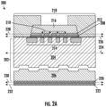
- FIG. 2A illustrates an example SiC power device 200 in accordance with one or more embodiments of the present invention.
- the SiC power device 200 may be fabricated using one or more of the improved fabrication techniques of the present invention.
- the SiC power device 200, or SiC power device 200 may include a semiconductor device with a plurality of material layers.
- the SiC power device 200 includes a semiconductor base material 202.
- the semiconductor base material 202 may include a SiC material.
- the SiC material may extend in lateral directions along a base plane 224.
- the SiC material may include a wide bandgap semiconductor material.
- the semiconductor base material 202 may include a first side and a second side.
- the first side may include an epitaxial drift layer 204.
- the second side may include a doped SiC substrate 206.
- the doped SiC substrate 206 for example, may be doped with one or more combinations of aluminum, boron, gallium, and/or the like to fabricate a P-type SiC power device.
- the doped SiC substrate 206 may be doped with one or more combinations of nitrogen, phosphorus, and/or the like to fabricate an N-type SiC power device.
- the semiconductor base material 202 includes one or more anode implants 214.
- the anode implants 214 may be disposed within the epitaxial drift layer 204.
- the anode implants 214 may extend vertically from a surface of the epitaxial drift layer 204 toward the base plane 224.
- the anode implants may include an epitaxially grown guard ring.
- the SiC power device 200 includes a first metallic layer 208 and/or a second metallic layer 212.
- the first metallic layer 208 may be disposed on the first side of the semiconductor base material 202.
- the first metallic layer 208 may be disposed on the surface of the epitaxial drift layer 204.
- the first metallic layer 208 may be disposed directly on the surface of the epitaxial drift layer 204.
- the first metallic layer 208 may cover the anode implants.
- the first metallic layer 208 for example, may extend laterally along a surface plane 226 of the epitaxial drift layer 204.
- the first metallic layer may include an electrically and/or thermally conductive metal, such as nickel material (chemical symbol Ni), gold (chemical symbol Au), germanium (chemical symbol Ge), tin (chemical symbol Sn), indium tin oxide, titanium (chemical symbol Ti), molybdenum (chemical symbol Mo), tungsten (chemical symbol W), titanium nitride (chemical symbol TiN), molybdenum nitride (chemical symbol MoN), tungsten nitride (chemical symbol WN), and/or the like.
- nickel material chemical symbol Ni
- gold chemical symbol Au
- germanium chemical symbol Ge
- tin chemical symbol Sn
- indium tin oxide titanium
- titanium molybdenum
- tungsten chemical symbol W
- titanium nitride chemical symbol TiN
- molybdenum nitride chemical symbol MoN
- tungsten nitride chemical symbol WN
- the first metallic layer 208 forms one or more ohmic contacts 210 and/or a Schottky contact for the SiC power device 200.
- the single, first metallic layer 208 may form both the ohmic contacts 210 and the Schottky contact.
- the first metallic layer 208 may form the one or more ohmic contacts 210 and the Schottky contact within a same plane (e.g., the surface plane 226).
- the one or more ohmic contacts 210 and the Schottky contact may be formed within a p+ region of the SiC device (e.g., to prevent short circuit behavior during biasing, etc.).
- a first portion of the first metallic layer 208 may form the one or more ohmic contacts 210 and/or a second portion of the first metallic layer 208 may form the Schottky contact.
- the one or more ohmic contacts may include one or more silicide portions (e.g., titanium silicides, etc.) on the first metallic layer 208.
- the one or more silicide portions may correspond to the one or more anode implants 214.
- the silicide portions may be disposed directly over one or more of the anode implants 214.
- the second metallic layer 212 is disposed on the first metallic layer 208.
- the second metallic layer 212 may be disposed directly on the first metallic layer 208.
- the second metallic layer 212 may extend laterally along a barrier plane 228 over the first metallic layer 208.
- the second metallic layer 212 may include one or more cutouts that expose one or more portions of the first metallic layer 208.
- the second metallic layer 212 may be disposed on a second portion of the first metallic layer 208 and expose a first portion (e.g., the ohmic contacts 210) of the first metallic layer 208.
- the second metallic layer may include a reflective metal, such as an aluminum material (chemical symbol Al), and/or the like.
- second metallic layer 212 may act as a barrier layer during the fabrication of the SiC power device 200.
- the second metallic layer 212 may not be sacrificial and may be part of the active area of the SiC power device 200.
- the first metallic layer 208 may be of a material that absorbs radiation (e.g., light) having a wavelength, in particular the radiation emitted by a laser usable for laser annealing, whereas the second metallic layer 212 may be of a material that reflects radiation having said same wavelength.
- radiation e.g., light
- the second metallic layer 212 may be of a material that reflects radiation having said same wavelength.
- the SiC power device 200 includes a frontside metallic layer 216 and/or a passivation layer 218.
- the frontside metallic layer 216 may include any type of metal layer including, as examples, aluminum, nickel, chromium, gold, germanium, copper, silver, titanium, tungsten, platinum, tantalum, and/or the like.
- the frontside metallic layer 216 may be disposed on the first metallic layer 208 and/or the second metallic layer 212.
- the frontside metallic layer 216 may directly cover the second metallic layer 212 and the exposed portions (e.g., the ohmic contacts 210) of the first metallic layer 208.
- the passivation layer 218 may include any type of insulating material, such as oxide, nitride, and/or the like.
- the passivation layer 218 may be disposed on the first side of the semiconductor base material 202.
- the passivation layer 218 may directly cover exposed surface portions of the epitaxial drift layer 204.
- the SiC power device 200 includes a backside ohmic contact 220 and/or a backside metallic layer 222.
- the backside ohmic contact 220 may extend laterally along a backside surface plane 230 over the surface of the second side (e.g., doped SiC substrate 206) of the semiconductor base material 202.
- the backside ohmic contact 220 may include any electrically and/or thermally conductive metal including, as examples, nickel (chemical symbol Ni), gold (chemical symbol Au), germanium (chemical symbol Ge), tin (chemical symbol Sn), indium tin oxide, and/or the like.
- the backside metallic layer 222 may extend laterally along a second plane 232 over the surface of the backside ohmic contact 220.
- the backside metallic layer 222 may include any type of metal layer including, as examples, aluminum, nickel, chromium, gold, germanium, copper, silver, titanium, tungsten, platinum, tantalum, and/or the like.
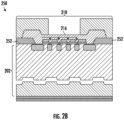
- FIG. 2B illustrates another example SiC power device 250 in accordance with one or more embodiments of the present invention.
- the SiC power device 250 may be fabricated using one or more of the improved fabrication techniques of the present disclosure.
- the SiC power device 250 may include a semiconductor device with a plurality of material layers including some of the metal layers described herein with reference to SiC power device 200.
- the SiC power device 250 may include a SiC power device with a field plate edge termination.
- the SiC power device 250 may include one or more dielectric layers 252.
- the dielectric layers 252 may cover one or more peripheral portions of the semiconductor base material 202.
- the dielectric layers 252 may separate the semiconductor base material 202 from the passivation layer 218 and the frontside metallic layer 216.
- the SiC power devices 200 and 250 may be fabricated using improved semiconductor fabrication techniques. Some improved fabrication techniques will be described in further detail with reference to FIGS. 3A-3D .
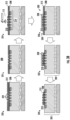
- FIG. 3A illustrates an example first stage of a fabrication process 300 for fabricating a SiC device in accordance with one or more embodiments of the present invention.
- the first stage may include a first fabrication operation 302.
- a semiconductor base material 202 may be provided.
- the semiconductor base material 202 may include a first side 202A and a second side 202B.
- the semiconductor base material 202 may include a SiC material.
- the first side 202A may include an epitaxial drift layer 204 and the second side 202B may include a doped SiC substrate 206.
- an anode mask 304 may be placed over the first side 202A of the semiconductor base material 202.
- the anode mask 304 may include a patterned mask with one or more cutouts for one or more anode implants. An anode implantation operation may be applied through the anode mask 304 to form one or more anode implants within the epitaxial drift layer 204 of the semiconductor base material 202.
- the first stage may include a second fabrication operation 306.
- the anode mask 304 may be removed from the surface of the first side 202A of the semiconductor base material 202.
- the first stage may include a third fabrication operation 308, during which the one or more anode implants 214 may be formed within the first side 202A (e.g., the epitaxial drift layer 204) of the semiconductor base material 202.
- the third fabrication operation 308 may include a dopant activation.
- the dopant activation may include a high temperature annealing (e.g., ⁇ 1600°C, etc.).
- the first stage may include a fourth fabrication operation 310.
- a first metallic layer 208 may be formed on a first side 202A of the semiconductor base material 202 to form a Schottky contact.
- the first metallic layer 208 may be formed using one or more metal deposition techniques, such as one or more laser metal deposition, direct metal deposition, cold spray metal deposition, and/or the like.
- the first metallic layer may include a titanium-based material and/or any other electrically and/or thermally conductive metal (e.g., nickel-based, etc.).
- the first stage may include a fifth fabrication operation 312.
- a second metallic layer 212 may be formed over the first metallic layer 208 to form a reflective barrier layer covering the Schottky contact.
- the second metallic layer 212 may be formed using one or more metal deposition techniques, described herein.
- the second metallic layer may include an aluminum-based material and/or any other reflective metal.
- the first stage may include a sixth fabrication operation 314.
- a patterned mask 316 may be placed over the second metallic layer 212.
- the patterned mask 316 may expose one or more portions 318 of the second metallic layer 212.
- FIG. 3B illustrates an example second stage of a fabrication process 300 for fabricating a SiC device in accordance with one or more embodiments of the present invention, which may follow the first stage of FIG. 3A .
- the second stage may include a seventh fabrication operation 320.
- the one or more exposed portions of the second metallic layer 212 may be removed to expose a first portion 322 of the first metallic layer 208.
- the one or more exposed portions of the second metallic layer 212 may be etched to expose the first portion 322 of the first metallic layer 208.
- the second metallic layer 212 may be etched, through the patterned mask 316, to remove the one or more portions of the second metallic layer 212 and expose the first portion 322 of the first metallic layer 208.
- the second metallic layer 212 may be etched using one or more etching techniques, such as chemical etching, mechanical etching, wet etching, dry etching, and/or the like.
- the second stage may include an eighth fabrication operation 321, during which the patterned mask 316 may be removed from the second metallic layer 212.
- the second stage may include a ninth fabrication operation 324.
- one or more silicide portions e.g., titanium silicide, etc.
- the first metallic layer 208 may form one or more ohmic contacts 210 within the Schottky contact.
- the one or more silicide portions may be formed through a laser annealing process.
- the laser annealing process may include applying a laser annealing machine 112 to the first metallic layer 208 through the reflective layer of the second metallic layer 212. In this way, the first metallic layer 208 may form the one or more ohmic contacts 210 and/or the Schottky contact within a same plane.
- the one or more silicide portions on the first metallic layer 208 may correspond to the one or more anode implants 214.
- each silicide portion may align with at least one of the one or more anode implants 214.
- ohmic contacts 210 and/or Schottky contacts may be formed on the p+ region of the SiC device to guarantee the right onset of the PN junction when high current flow is needed.
- the second stage may include a tenth fabrication operation 326.
- an interior mask 328 may be placed over the second metallic layer 212.
- the interior mask 328 may expose one or more peripheral portions 330 of the second metallic layer 212, while covering an interior portion of the second metallic layer 212 and the first metallic layer 208 including the ohmic contacts 210.
- the second stage may include an eleventh fabrication operation 332.
- the eleventh fabrication operation 332 subsequent to forming the one or more silicide portions on the first metallic layer 208, the one or more peripheral portions 330 of the first metallic layer 208 and the second metallic layer 212 may be removed to expose at least a portion of the semiconductor base material 202.
- the second metallic layer 212 and/or the first metallic layer 208 may be etched, around the interior mask 328, to remove the one or more peripheral portions 330 of the second metallic layer 212 and/or the first metallic layer 208.
- the first and second metallic layers may be etched using any etching process, such as those described herein.
- the second stage may include a twelfth fabrication operation 334, during which the interior mask 328 may be removed to expose the interior portion of the second metallic layer 212 and the first metallic layer 208 including the ohmic contacts 210.
- FIG. 3C illustrates an example third stage of a fabrication process 300 for fabricating a SiC device in accordance with one or more embodiments of the present invention, which may follow the second stage of FIG. 3B .
- the third stage may include a thirteenth fabrication operation 336.
- a dielectric layer 338 may be formed on the first side 202A of the semiconductor base material 202.
- the dielectric layer 338 may cover the semiconductor base material 202, the first metallic layer 208, and/or the second metallic layer 212.
- the third stage may include a fourteenth fabrication operation 340.
- a dielectric layer mask 344 may be placed over one or more peripheral dielectric portions 342 of the dielectric layer 338.
- an interior dielectric portion may be etched from the dielectric layer 338 to expose the second metallic layer 212 and/or the one or more silicide portions (e.g., ohmic contacts 210) on the first metallic layer 208.
- the dielectric layer mask 344 may be removed to expose the peripheral dielectric portions 342 of the dielectric layer 338.
- the third stage may include a seventeenth fabrication operation 350.
- a frontside metallic layer 352 may be formed over the first side 202A of the semiconductor base material 202, the dielectric layer 338, the first metallic layer 208, and/or the second metallic layer 212.
- the third stage may include an eighteenth fabrication operation 354, during which a frontside metallic layer mask 356 may be placed over an interior portion of the frontside metallic layer 352.
- FIG. 3D illustrates an example fourth stage of a fabrication process 300 for fabricating a SiC device in accordance with one or more embodiments of the present invention, which may follow the third stage of FIG. 3C .
- the fourth stage may include a nineteenth fabrication operation 358.
- a peripheral frontside metallic portion may be removed from the frontside metallic layer 352 to expose the dielectric layer 338.
- the peripheral frontside metallic portion may be etched, around the frontside metallic layer mask 356, to remove the peripheral frontside metallic portion from the frontside metallic layer 352 and expose the dielectric layer 338.
- the fourth stage may include a twentieth fabrication operation 360, during which the frontside metallic layer mask 356 may be removed to expose the frontside metallic layer 352.
- the fourth stage may include a twenty-first fabrication operation 362.
- a passivation layer 364 may be formed over the dielectric layer 338 and the frontside metallic layer 352.
- the passivation layer may include an oxide and/or nitride layer that is formed by performing one or more plasma enhanced chemical vapor deposition and/or any other deposition techniques.
- the fourth stage may include a twenty-second fabrication operation 366. During the twenty-second fabrication operation 366, a passivation layer mask 368 may be placed over a peripheral portion of the passivation layer 364.
- the fourth stage may include a twenty-third fabrication operation 370.
- an interior passivation layer portion may be removed (e.g., etched, etc.) from the passivation layer 364 to expose the frontside metallic layer 352.
- the fourth stage may include a twenty-fourth fabrication operation 372.
- the passivation layer mask 368 may be removed to expose the passivation layer 364.
- a backside ohmic contact 374 may be formed on the second side 202B of the semiconductor base material 202.
- the backside metallic layer 376 may be formed over the backside ohmic contact 374.
- FIG. 4 illustrates a flowchart of an example method 400 for fabricating a SiC device in accordance with one or more embodiments of the present invention.
- the flowchart depicts techniques for overcoming various limitations of traditional SiC fabrication processes for fabricating SiC power devices.
- the techniques may be implemented by one or more computing devices, entities, and/or systems described herein.
- a computing device such as the computing apparatus 110 described herein, may implement the techniques (e.g., via one or more control instructions to one or more computing entities 120) to overcome the various limitations with traditional SiC fabrication processes by maximizing surge peak forward current (IFSM) ruggedness of Merged Pin Schottky Diode in Silicon Carbide, minimizing and simplifying fabrication process flow, avoiding metal scraps due to nickel silicide protrusion and nickel residual, among other advantages.
- IFSM surge peak forward current
- example method 400 depicts a particular sequence of steps/operations, the sequence may be altered without departing from the scope of the present invention, as defined in the appended claims. For example, some of the steps/operations depicted may be performed in parallel or in a different sequence that does not materially impact the function of the method 400. In other examples, different components of an example device or system that implements the method 400 may perform functions at substantially the same time or in a specific sequence.
- the method 400 includes, at step/operation 402, providing a semiconductor base material.
- the method 400 may include providing a semiconductor base material that includes a first side and a second side.
- the semiconductor base material may include a silicon carbide material.
- the method 400 includes, at step/operation 404, forming a first metallic layer.
- the method 400 may include forming a first metallic layer on a first side of the semiconductor base material to form a Schottky contact.
- the method 400 includes, at step/operation 406, forming a second metallic layer over the first metallic layer.
- the method 400 may include forming a second metallic layer over the first metallic layer to form a reflective barrier layer covering the Schottky contact.
- the method 400 includes, at step/operation 408, removing a portion of the second metallic layer to expose the first metallic layer.
- the method 400 may include removing one or more portions of the second metallic layer to expose a first portion of the first metallic layer.
- the method 400 may include placing a patterned mask over the second metallic layer. The patterned mask may expose the one or more portions of the second metallic layer.
- the method 400 may include etching the second metallic layer, through the patterned mask, to remove the one or more portions of the second metallic layer and then removing the patterned mask.
- the method 400 includes, at step/operation 410, applying a laser annealing process to form silicide portions on the first metallic layer.
- the method 400 may include forming, through a laser annealing process, one or more silicide portions on the first metallic layer to form one or more ohmic contacts within the Schottky contact.
- the first metallic layer forms the one or more ohmic contacts and the Schottky contact within a same plane.
- the one or more ohmic contacts and the Schottky contact may be formed in a p+ region of the SiC device to prevent short circuit behavior during biasing.
- the method 400 may include removing one or more peripheral portions of the first metallic layer and the second metallic layer to expose at least a portion of the semiconductor base material.
- the method 400 may include placing an interior mask over the second metallic layer. The interior mask may expose the one or more peripheral portions of the second metallic layer.
- the method 400 may include etching the second metallic layer and the first metallic layer, around the interior mask, to remove the one or more peripheral portions of the second metallic layer and the first metallic layer and then removing the interior mask.
- the method 400 includes, at step/operation 412, forming a dielectric layer.
- the method 400 may include, subsequent to forming the one or more silicide portions on the first metallic layer, forming the dielectric layer on the first side of the semiconductor base material.
- the dielectric layer may cover the semiconductor base material, the first metallic layer, and the second metallic layer.
- the method 400 may include placing a dielectric layer mask over one or more peripheral dielectric portions of the dielectric layer.
- the method may include etching an interior dielectric portion from the dielectric layer to expose the second metallic layer and the one or more silicide portions on the first metallic layer and then removing the dielectric layer mask.
- the method 400 includes, at step/operation 414, forming a frontside metallic layer.
- the method 400 may include forming a frontside metallic layer over the first side of the semiconductor base material, the dielectric layer, the first metallic layer, and the second metallic layer.
- the method 400 may include placing a frontside metallic layer mask over an interior portion of the frontside metallic layer.
- the method 400 may include etching a peripheral frontside metallic portion from the frontside metallic layer to expose the dielectric layer and removing the frontside metallic layer mask.
- the method 400 includes, at step/operation 416, forming a passivation layer.
- the method 400 may include forming a passivation layer over the dielectric layer and the frontside metallic layer.
- the method 400 may include placing a passivation layer mask over a peripheral portion of the passivation layer.
- the method 400 may include etching an interior passivation layer portion from the passivation layer to expose the frontside metallic layer and then removing the passivation layer mask.
- the method 400 may include forming a backside ohmic contact on the second side of the semiconductor base material and then forming a backside metallic layer over the backside ohmic contact.
Landscapes
- Electrodes Of Semiconductors (AREA)
- Engineering & Computer Science (AREA)
- Manufacturing & Machinery (AREA)
Abstract
Various embodiments of the present disclosure disclose improved silicon carbide (SiC) power devices and methods of fabrication of such devices. A SiC power device includes a semiconductor base material with a first side and a second side and a first metallic layer disposed on the first side of the semiconductor base material that forms ohmic contacts and Schottky contacts. The SiC power device may be fabricated by forming a first metallic layer on a first side of a semiconductor base material to form a Schottky contact, forming a second metallic layer over the first metallic layer to form a reflective barrier covering the Schottky contact, removing one or more portions of the second metallic layer to expose a first portion of the first metallic layer, and forming silicide portions on the first metallic layer to form ohmic contacts within the Schottky contact.
Description
- The present invention relates to the field of silicon carbide (SiC) power devices, and in particular, to front side ohmic contact formations for SiC power devices.
- Applicant has identified many technical challenges and difficulties associated with SiC devices, such as the SiC power devices, in particular problems related to the fabrication of SiC power devices.
- Traditionally, complex process flows are needed to realize ohmic contact formations on p+ and/or n+ regions of SiC devices. An ohmic contact formation may require a (i) metal deposition, such as a nickel or other conductive material, (ii) an annealing temperature at near 1000°C to trigger a reaction between the metal deposition and the SiC (e.g., to form of silicides, titanium silicides, etc.), and (iii) the removal of portions of the metal deposition that are in direct contact with the SiC surface. The selective removal of portions of the metal deposition may be complex and, in part due to the complexity, is unreliable and prone to errors, while being critical to the functionality of SiC devices. Thus, traditional techniques for fabricating SiC devices face technical challenges that decrease their reliability, while increasing the rate of failure as well as the cost and expense of fabrication.
- Thus, an aim of the present invention is to overcome the disadvantages of the prior art.
- According to the present invention, a method, in particular a method for fabricating a SiC device, and a SiC device are provided, as defined in the appended claims.
- A method includes providing a semiconductor base material comprising a first side and a second side, wherein the semiconductor base material comprises a silicon carbide (SiC) material; forming a first metallic layer on a first side of the semiconductor base material to form a Schottky contact; forming a second metallic layer over the first metallic layer to form a reflective barrier layer covering the Schottky contact; removing one or more portions of the second metallic layer to expose a first portion of the first metallic layer; and forming, through a laser annealing process, one or more silicide portions on the first metallic layer to form one or more ohmic contacts within the Schottky contact.
- In some embodiments, the first metallic layer forms the one or more ohmic contacts and the Schottky contact within a p+ region.
- In some embodiments, the method further includes, subsequent to forming the one or more silicide portions on the first metallic layer, forming a dielectric layer on the first side of the semiconductor base material. The dielectric layer may cover the semiconductor base material, the first metallic layer, and the second metallic layer.
- In some embodiments, the method includes placing a dielectric layer mask over one or more peripheral dielectric portions of the dielectric layer; etching an interior dielectric portion from the dielectric layer to expose the second metallic layer and the one or more silicide portions on the first metallic layer; and removing the dielectric layer mask.
- In some embodiments, the method includes forming a frontside metallic layer over the first side of the semiconductor base material, the dielectric layer, the first metallic layer, and the second metallic layer; placing a frontside metallic layer mask over an interior portion of the frontside metallic layer; etching a peripheral frontside metallic portion from the frontside metallic layer to expose the dielectric layer; and removing the frontside metallic layer mask.
- In some embodiments, the method includes forming a passivation layer over the dielectric layer and the frontside metallic layer; placing a passivation layer mask over a peripheral portion of the passivation layer; etching an interior passivation layer portion from the passivation layer to expose the frontside metallic layer; and removing the passivation layer mask.
- In some embodiments, removing the one or more portions of the second metallic layer includes placing a patterned mask over the second metallic layer. The patterned mask may expose the one or more portions of the second metallic layer. The method may include etching the second metallic layer, through the patterned mask, to remove the one or more portions of the second metallic layer; and removing the patterned mask.
- In some embodiments, the method includes, subsequent to forming the one or more silicide portions on the first metallic layer, removing one or more peripheral portions of the first metallic layer and the second metallic layer to expose at least a portion of the semiconductor base material.
- In some embodiments, removing the one or more peripheral portions of the first metallic layer includes placing an interior mask over the second metallic layer, wherein the interior mask exposes the one or more peripheral portions of the second metallic layer; etching the second metallic layer and the first metallic layer, around the interior mask, to remove the one or more peripheral portions of the second metallic layer and the first metallic layer; and removing the interior mask.
- In some embodiments, the semiconductor base material includes one or more anode implants and the one or more silicide portions on the first metallic layer correspond to the one or more anode implants.
- In some embodiments, the method includes forming the one or more anode implants within the first side of the semiconductor base material.
- In some embodiments, the first side of the semiconductor base material includes an epitaxial drift layer and the second side of the semiconductor base material includes a doped SiC substrate.
- In some embodiments, the method includes forming a backside ohmic contact on the second side of the semiconductor base material; and forming a backside metallic layer over the backside ohmic contact.
- In some embodiments, the first metallic layer includes a nickel-based material.
- In some embodiments, the second metallic layer includes an aluminum-based material.
- A silicon carbide (SiC) power device includes a semiconductor base material with a first side and a second side; a first metallic layer disposed on the first side of the semiconductor base material, wherein a first portion of the first metallic layer forms one or more ohmic contacts and a second portion of the first metallic layer forms a Schottky contact; and a second metallic layer disposed on the second portion of the first metallic layer.
- In some embodiments, the first side of the semiconductor base material includes an epitaxial drift layer.
- In some embodiments, the second side of the semiconductor base material includes a doped SiC substrate.
- In some embodiments, the first metallic layer includes a nickel material.
- In some embodiments, the second metallic layer includes an aluminum material.
- The above summary is provided merely for purposes of summarizing some example embodiments to provide a basic understanding of some aspects of the disclosure. Accordingly, it will be appreciated that the above-described embodiments are merely examples and should not be construed to narrow the scope or spirit of the disclosure in any way. It will also be appreciated that the scope of the disclosure encompasses many potential embodiments in addition to those here summarized, some of which will be further described below.
- For a better understanding of the present invention, embodiments are now described, purely as non-limitative examples, with reference to the accompanying drawings, which are not necessarily drawn to scale, and wherein:
-
FIG. 1 illustrates an example computing entity in accordance with the present invention; -
FIGS. 2A and2B illustrate SiC power devices in accordance with embodiments of the present invention; -
FIGS. 3A-3D illustrate example stages for fabricating a SiC device in accordance with embodiments of the present invention; and -
FIG. 4 illustrates a flowchart of a method for fabricating a SiC device in accordance with embodiments of the present invention. - Embodiments of the present invention will now be described more fully herein with reference to the accompanying drawings. Like reference numerals refer to like elements throughout.
- Various example embodiments of the present disclosure are directed to improved SiC devices and systems, apparatuses, products, and methods for fabricating improved SiC devices. The present disclosure, in some examples, describes a method for the realization of front side ohmic contacts for SiC Merged PiN Schottky (MPS) devices, among other SiC devices, that improve upon traditional techniques for fabricating SiC devices.
- To address the above-described technical challenges for fabricating SiC devices, some embodiments of the present disclosure provide an improved SiC formation that includes a single layer of metal to realize both a Schottky contact and ohmic contact. The Schottky contact and the Ohmic contact may be realized through a laser annealing process by shielding the single layer of metal by a patterned second metal layer.
- Each layer may not be sacrificial and may be part of an active area of the SiC device; thereby reducing the risk of damaging the SiC device by removing metal layers in direct contact with a SiC surface.
- The fabricating process includes providing a semiconductor base material with a first side and a second side, forming a first metallic layer on a first side of the semiconductor base material to form a Schottky contact, forming a second metallic layer over the first metallic layer to form a reflective barrier layer covering the Schottky contact, removing one or more portions of the second metallic layer to expose a first portion of the first metallic layer; and forming, through a laser annealing process, one or more silicide portions (e.g., titanium silicides, etc.) on the first metallic layer to form one or more ohmic contacts within the Schottky contact. By doing so, the technical challenges related to SiC devices are addressed by eliminating the need to remove a metal deposition in direct contact with the SiC surface. In this way, it may be possible to prevent damage to SiC devices during fabrication, while reducing fabrication costs, efficiency, and reliability.
- It should be readily appreciated that the embodiments of the systems, apparatus, and methods described herein may be configured in various additional and alternative manners in addition to those expressly described herein.
-
FIG. 1 illustrates anexample computing system 100 in accordance with one or more embodiments of the present disclosure. In general, the terms computing system, computer, system, device, entity, and/or similar words used herein interchangeably may refer to, for example, one or more computers, computing entities, desktops, mobile phones, tablets, notebooks, laptops, distributed systems, kiosks, input terminals, servers or server networks, blades, gateways, switches, processing devices, processing entities, set-top boxes, relays, routers, network access points, base stations, the like, and/or any combination of devices or entities adapted to perform the functions, operations, and/or processes described herein. Such functions, operations, and/or processes may include, for example, transmitting, receiving, operating on, processing, displaying, storing, determining, creating/generating, monitoring, evaluating, comparing, and/or similar terms used herein interchangeably. In one embodiment, these functions, operations, and/or processes may be performed on data, content, information, and/or similar terms used herein interchangeably. - The
computing system 100 may include acomputing apparatus 110 and/or one ormore computing entities 120 communicatively coupled to thecomputing apparatus 110 using one or more wired and/or wireless communication techniques. Thecomputing apparatus 110 may include any computing device including, for example, one or more services, computing platforms, and/or the like, that are specially configured to perform one or more steps/operations of the one or more fabrication techniques described herein. In some embodiments, thecomputing apparatus 110 may include and/or be in association with one or more mobile device(s), desktop computer(s), laptop(s), server(s), cloud computing platform(s), and/or the like. In some example embodiments, thecomputing apparatus 110 may be configured to receive and/or provide power conversion instructions, data, and/or the like between the one ormore computing entities 120 to perform one or more steps/operations of one or more fabrication techniques described herein. - In some embodiments, the
computing apparatus 110 includes, is integrated with, and/or is otherwise in association with one ormore computing entities 120. The one ormore computing entities 120 may include one or more semiconductor fabrication devices, such as one or more reactive etching devices 114 (e.g., ion-etching device, chemical etching devices, physical etching devices, etc.), one or more laser annealing machines 112 (e.g., ultraviolet lasers, fiber lasers, carbon dioxide lasers, etc.), chemical, physical, atomic, and/or the like deposition devices (e.g., plasma-enhanced chemical vapor deposition (PECVD), sputter vapor deposition, thermal evaporation, arc vapor deposition, etc.). For example, thecomputing apparatus 110 may be configured to receive and/or provide one or more fabrication instructions between one or more components of the one ormore computing entities 120. The computingentities 120, for example, may include and/or be associated with one or more fabrication systems configured to perform one or more fabrication operations for fabricating SiC, and/or other power devices. The one or more fabrication systems, for example, may be configured to fabricate one or more SiC power devices (e.g., MOSFETs, Diodes, IGBTs, etc.) for use with one or more converters, inverters, power supplies, battery chargers, motor control systems, and/or the like. - The
computing apparatus 110 may include, or be in communication with, one or more processing elements 102 (also referred to as processors, processing circuitry, digital circuitry, and/or similar terms used herein interchangeably) that communicate with other elements within thecomputing apparatus 110 via a bus, for example. As will be understood, theprocessing element 102 may be embodied in a number of different ways. - For example, the
processing element 102 may be embodied as one or more complex programmable logic devices (CPLDs), microprocessors, multi-core processors, coprocessing entities, application-specific instruction-set processors (ASIPs), microcontrollers, and/or controllers. Further, theprocessing element 102 may be embodied as one or more other processing devices or circuitry. The term circuitry may refer to an entirely hardware embodiment or a combination of hardware and computer program products. Thus, theprocessing element 102 may be embodied as integrated circuits, application specific integrated circuits (ASICs), field programmable gate arrays (FPGAs), programmable logic arrays (PLAs), hardware accelerators, digital circuitry, and/or the like. - As will therefore be understood, the
processing element 102 may be configured for a particular use or configured to execute instructions stored in volatile or non-volatile media or otherwise accessible to theprocessing element 102. As such, whether configured by hardware or computer program products, or by a combination thereof, theprocessing element 102 may be capable of performing steps or operations according to embodiments of the present disclosure when configured accordingly. - In one embodiment, the
computing apparatus 110 may further include, or be in communication with, one ormore memory elements 104. The one ormore memory elements 104 may include non-volatile and/or volatile media. Thememory elements 104, for example, may include non-volatile media (also referred to as non-volatile storage, memory, memory storage, memory circuitry and/or similar terms used herein interchangeably). In one embodiment, the non-volatile storage or memory may include one or more non-volatile storage or memory media, including, but not limited to, hard disks, ROM, PROM, EPROM, EEPROM, flash memory, MMCs, SD memory cards, Memory Sticks, CBRAM, PRAM, FeRAM, NVRAM, MRAM, RRAM, SONOS, FJG RAM, Millipede memory, racetrack memory, and/or the like. - As will be recognized, the non-volatile storage or memory media may store databases, database instances, database management systems, data, applications, programs, program modules, scripts, source code, object code, byte code, compiled code, interpreted code, machine code, executable instructions, and/or the like. The term database, database instance, database management system, and/or similar terms used herein interchangeably may refer to a collection of records or data that is stored in a computer-readable storage medium using one or more database models, such as a hierarchical database model, network model, relational model, entity-relationship model, object model, document model, semantic model, graph model, and/or the like.
- In addition, or alternatively, the
memory elements 104 may include volatile memory. For example, thecomputing apparatus 110 may further include, or be in communication with, volatile media (also referred to as volatile storage memory, memory storage, memory circuitry and/or similar terms used herein interchangeably). In one embodiment, the volatile storage or memory may also include one or more volatile storage or memory media, including, but not limited to, RAM, DRAM, SRAM, FPM DRAM, EDO DRAM, SDRAM, DDR SDRAM, DDR2 SDRAM, DDR3 SDRAM, RDRAM, TTRAM, T-RAM, Z-RAM, RIMM, DIMM, SIMM, VRAM, cache memory, register memory, and/or the like. - As will be recognized, the volatile storage or memory media may be used to store at least portions of the databases, database instances, database management systems, data, applications, programs, program modules, scripts, source code, object code, byte code, compiled code, interpreted code, machine code, executable instructions, and/or the like being executed by, for example, the
processing element 102. Thus, the databases, database instances, database management systems, data, applications, programs, program modules, scripts, source code, object code, byte code, compiled code, interpreted code, machine code, executable instructions, and/or the like may be used to control certain aspects of the operation of thecomputing apparatus 110 with the assistance of theprocessing element 102 and operating system. - As indicated, in one embodiment, the
computing apparatus 110 may also include one ormore communication interfaces 108 for communicating with various computing entities, including computingentities 120, such as by communicating data, content, information, and/or similar terms used herein interchangeably that may be transmitted, received, operated on, processed, displayed, stored, and/or the like. The one ormore communication interfaces 108, for example, may include one or more wired peripherals (e.g., fiber interfaces, ethernet ports, and/or the like), antenna, transmitters, receivers, digital to analog converters (DAC), analog to digital converters (ADC), modulators, demodulators, and/or the like. Such communication may be executed using a wired data transmission protocol, such as fiber distributed data interface (FDDI), digital subscriber line (DSL), Ethernet, asynchronous transfer mode (ATM), frame relay, data over cable service interface specification (DOCSIS), or any other wired transmission protocol. Similarly, thecomputing apparatus 110 may be configured to communicate via wireless external communication networks using any of a variety of protocols, such as general packet radio service (GPRS), Universal Mobile Telecommunications System (UMTS), Code Division Multiple Access 2000 (CDMA2000), CDMA2000 IX (1xRTT), Wideband Code Division Multiple Access (WCDMA), Global System for Mobile Communications (GSM), Enhanced Data rates for GSM Evolution (EDGE), Time Division-Synchronous Code Division Multiple Access (TD-SCDMA), Long Term Evolution (LTE), Evolved Universal Terrestrial Radio Access Network (E-UTRAN), Evolution-Data Optimized (EVDO), High Speed Packet Access (HSPA), High-Speed Downlink Packet Access (HSDPA), IEEE 802.9 (Wi-Fi), Wi-Fi Direct, 802.16 (WiMAX), ultra-wideband (UWB), infrared (IR) protocols, NFC protocols such as NFC-A, NFC-B, NFC-F, Wibree, Bluetooth protocols, wireless universal serial bus (USB) protocols, and/or any other wireless protocol. - The
computing apparatus 110 may include input/output circuitry for communicating with one or more users. The input/output circuitry, for example, may include one or more user interfaces for providing and/or receiving information from one or more users of thecomputing apparatus 110. The input/output interfaces may include one or more tactile interfaces (e.g., keypads, touch screens, etc.), one or more audio interfaces (e.g., microphones, speakers, etc.), visual interfaces (e.g., display devices, etc.), and/or the like. The input/output circuitry may be configured to receive user input through one or more of the user interfaces from a user ofcomputing apparatus 110 and provide data to a user through one or more of the user interfaces. - Example embodiments of the present disclosure describe an improved SiC power device structure that may be fabricated using improved fabrication techniques. The improved fabrication techniques eliminate the need to remove metallic material in contact with a SiC surface, which reduces fabrication complexity and risk of damage among other benefits described herein.
-
FIG. 2A illustrates an exampleSiC power device 200 in accordance with one or more embodiments of the present invention. TheSiC power device 200 may be fabricated using one or more of the improved fabrication techniques of the present invention. TheSiC power device 200, orSiC power device 200, may include a semiconductor device with a plurality of material layers. - The
SiC power device 200 includes asemiconductor base material 202. Thesemiconductor base material 202 may include a SiC material. The SiC material may extend in lateral directions along abase plane 224. In some examples, the SiC material may include a wide bandgap semiconductor material. Thesemiconductor base material 202 may include a first side and a second side. The first side may include anepitaxial drift layer 204. The second side may include adoped SiC substrate 206. Thedoped SiC substrate 206, for example, may be doped with one or more combinations of aluminum, boron, gallium, and/or the like to fabricate a P-type SiC power device. In addition, or alternatively, thedoped SiC substrate 206 may be doped with one or more combinations of nitrogen, phosphorus, and/or the like to fabricate an N-type SiC power device. - In some embodiments, the
semiconductor base material 202 includes one ormore anode implants 214. Theanode implants 214 may be disposed within theepitaxial drift layer 204. In some examples, theanode implants 214 may extend vertically from a surface of theepitaxial drift layer 204 toward thebase plane 224. In some examples, the anode implants may include an epitaxially grown guard ring. - In some embodiments, the
SiC power device 200 includes a firstmetallic layer 208 and/or a secondmetallic layer 212. The firstmetallic layer 208 may be disposed on the first side of thesemiconductor base material 202. For example, the firstmetallic layer 208 may be disposed on the surface of theepitaxial drift layer 204. The firstmetallic layer 208 may be disposed directly on the surface of theepitaxial drift layer 204. In some examples, the firstmetallic layer 208 may cover the anode implants. The firstmetallic layer 208, for example, may extend laterally along asurface plane 226 of theepitaxial drift layer 204. The first metallic layer may include an electrically and/or thermally conductive metal, such as nickel material (chemical symbol Ni), gold (chemical symbol Au), germanium (chemical symbol Ge), tin (chemical symbol Sn), indium tin oxide, titanium (chemical symbol Ti), molybdenum (chemical symbol Mo), tungsten (chemical symbol W), titanium nitride (chemical symbol TiN), molybdenum nitride (chemical symbol MoN), tungsten nitride (chemical symbol WN), and/or the like. - In some embodiments, the first
metallic layer 208 forms one or moreohmic contacts 210 and/or a Schottky contact for theSiC power device 200. For instance, the single, firstmetallic layer 208 may form both theohmic contacts 210 and the Schottky contact. The firstmetallic layer 208 may form the one or moreohmic contacts 210 and the Schottky contact within a same plane (e.g., the surface plane 226). By way of example, the one or moreohmic contacts 210 and the Schottky contact may be formed within a p+ region of the SiC device (e.g., to prevent short circuit behavior during biasing, etc.). - For example, a first portion of the first
metallic layer 208 may form the one or moreohmic contacts 210 and/or a second portion of the firstmetallic layer 208 may form the Schottky contact. In some examples, the one or more ohmic contacts may include one or more silicide portions (e.g., titanium silicides, etc.) on the firstmetallic layer 208. The one or more silicide portions may correspond to the one ormore anode implants 214. For example, the silicide portions may be disposed directly over one or more of theanode implants 214. - In some embodiments, the second
metallic layer 212 is disposed on the firstmetallic layer 208. For example, the secondmetallic layer 212 may be disposed directly on the firstmetallic layer 208. The secondmetallic layer 212, for example, may extend laterally along abarrier plane 228 over the firstmetallic layer 208. In some examples, the secondmetallic layer 212 may include one or more cutouts that expose one or more portions of the firstmetallic layer 208. For instance, the secondmetallic layer 212 may be disposed on a second portion of the firstmetallic layer 208 and expose a first portion (e.g., the ohmic contacts 210) of the firstmetallic layer 208. The second metallic layer may include a reflective metal, such as an aluminum material (chemical symbol Al), and/or the like. As described herein, secondmetallic layer 212 may act as a barrier layer during the fabrication of theSiC power device 200. The secondmetallic layer 212 may not be sacrificial and may be part of the active area of theSiC power device 200. - In practice, according to an embodiment, the first
metallic layer 208 may be of a material that absorbs radiation (e.g., light) having a wavelength, in particular the radiation emitted by a laser usable for laser annealing, whereas the secondmetallic layer 212 may be of a material that reflects radiation having said same wavelength. - In some embodiments, the
SiC power device 200 includes a frontsidemetallic layer 216 and/or apassivation layer 218. The frontsidemetallic layer 216 may include any type of metal layer including, as examples, aluminum, nickel, chromium, gold, germanium, copper, silver, titanium, tungsten, platinum, tantalum, and/or the like. The frontsidemetallic layer 216 may be disposed on the firstmetallic layer 208 and/or the secondmetallic layer 212. For example, the frontsidemetallic layer 216 may directly cover the secondmetallic layer 212 and the exposed portions (e.g., the ohmic contacts 210) of the firstmetallic layer 208. Thepassivation layer 218 may include any type of insulating material, such as oxide, nitride, and/or the like. Thepassivation layer 218 may be disposed on the first side of thesemiconductor base material 202. For example, thepassivation layer 218 may directly cover exposed surface portions of theepitaxial drift layer 204. - In some embodiments, the
SiC power device 200 includes a backsideohmic contact 220 and/or a backsidemetallic layer 222. The backsideohmic contact 220 may extend laterally along abackside surface plane 230 over the surface of the second side (e.g., doped SiC substrate 206) of thesemiconductor base material 202. The backsideohmic contact 220 may include any electrically and/or thermally conductive metal including, as examples, nickel (chemical symbol Ni), gold (chemical symbol Au), germanium (chemical symbol Ge), tin (chemical symbol Sn), indium tin oxide, and/or the like. The backsidemetallic layer 222 may extend laterally along asecond plane 232 over the surface of the backsideohmic contact 220. The backsidemetallic layer 222 may include any type of metal layer including, as examples, aluminum, nickel, chromium, gold, germanium, copper, silver, titanium, tungsten, platinum, tantalum, and/or the like. -
FIG. 2B illustrates another exampleSiC power device 250 in accordance with one or more embodiments of the present invention. TheSiC power device 250 may be fabricated using one or more of the improved fabrication techniques of the present disclosure. TheSiC power device 250 may include a semiconductor device with a plurality of material layers including some of the metal layers described herein with reference toSiC power device 200. In some examples, theSiC power device 250 may include a SiC power device with a field plate edge termination. For example, theSiC power device 250. For example, in addition to the metal, SiC, and/or passivation layers of theSiC power device 200, theSiC power device 250 may include one or moredielectric layers 252. Thedielectric layers 252 may cover one or more peripheral portions of thesemiconductor base material 202. For example, thedielectric layers 252 may separate thesemiconductor base material 202 from thepassivation layer 218 and the frontsidemetallic layer 216. - The
SiC power devices FIGS. 3A-3D . -
FIG. 3A illustrates an example first stage of afabrication process 300 for fabricating a SiC device in accordance with one or more embodiments of the present invention. The first stage may include afirst fabrication operation 302. During thefirst fabrication operation 302, asemiconductor base material 202 may be provided. Thesemiconductor base material 202 may include afirst side 202A and asecond side 202B. Thesemiconductor base material 202 may include a SiC material. In some examples, thefirst side 202A may include anepitaxial drift layer 204 and thesecond side 202B may include adoped SiC substrate 206. During thefirst fabrication operation 302, ananode mask 304 may be placed over thefirst side 202A of thesemiconductor base material 202. Theanode mask 304 may include a patterned mask with one or more cutouts for one or more anode implants. An anode implantation operation may be applied through theanode mask 304 to form one or more anode implants within theepitaxial drift layer 204 of thesemiconductor base material 202. - The first stage may include a
second fabrication operation 306. During thesecond fabrication operation 306, theanode mask 304 may be removed from the surface of thefirst side 202A of thesemiconductor base material 202. - The first stage may include a
third fabrication operation 308, during which the one ormore anode implants 214 may be formed within thefirst side 202A (e.g., the epitaxial drift layer 204) of thesemiconductor base material 202. In some examples, thethird fabrication operation 308 may include a dopant activation. The dopant activation may include a high temperature annealing (e.g., ~1600°C, etc.). - The first stage may include a
fourth fabrication operation 310. During thefourth fabrication operation 310, a firstmetallic layer 208 may be formed on afirst side 202A of thesemiconductor base material 202 to form a Schottky contact. The firstmetallic layer 208 may be formed using one or more metal deposition techniques, such as one or more laser metal deposition, direct metal deposition, cold spray metal deposition, and/or the like. In some examples, the first metallic layer may include a titanium-based material and/or any other electrically and/or thermally conductive metal (e.g., nickel-based, etc.). - The first stage may include a
fifth fabrication operation 312. During thefifth fabrication operation 312, a secondmetallic layer 212 may be formed over the firstmetallic layer 208 to form a reflective barrier layer covering the Schottky contact. The secondmetallic layer 212 may be formed using one or more metal deposition techniques, described herein. In some examples, the second metallic layer may include an aluminum-based material and/or any other reflective metal. - The first stage may include a
sixth fabrication operation 314. During thesixth fabrication operation 314, apatterned mask 316 may be placed over the secondmetallic layer 212. The patternedmask 316 may expose one ormore portions 318 of the secondmetallic layer 212. -
FIG. 3B illustrates an example second stage of afabrication process 300 for fabricating a SiC device in accordance with one or more embodiments of the present invention, which may follow the first stage ofFIG. 3A . - The second stage may include a
seventh fabrication operation 320. During theseventh fabrication operation 320, the one or more exposed portions of the secondmetallic layer 212 may be removed to expose afirst portion 322 of the firstmetallic layer 208. In some examples, the one or more exposed portions of the secondmetallic layer 212 may be etched to expose thefirst portion 322 of the firstmetallic layer 208. For example, the secondmetallic layer 212 may be etched, through the patternedmask 316, to remove the one or more portions of the secondmetallic layer 212 and expose thefirst portion 322 of the firstmetallic layer 208. The secondmetallic layer 212 may be etched using one or more etching techniques, such as chemical etching, mechanical etching, wet etching, dry etching, and/or the like. - The second stage may include an
eighth fabrication operation 321, during which the patternedmask 316 may be removed from the secondmetallic layer 212. - The second stage may include a
ninth fabrication operation 324. During theninth fabrication operation 324, one or more silicide portions (e.g., titanium silicide, etc.) may be formed on the firstmetallic layer 208 to form one or moreohmic contacts 210 within the Schottky contact. In some examples, the one or more silicide portions may be formed through a laser annealing process. The laser annealing process, for example, may include applying alaser annealing machine 112 to the firstmetallic layer 208 through the reflective layer of the secondmetallic layer 212. In this way, the firstmetallic layer 208 may form the one or moreohmic contacts 210 and/or the Schottky contact within a same plane. In some examples, the one or more silicide portions on the firstmetallic layer 208 may correspond to the one ormore anode implants 214. For example, each silicide portion may align with at least one of the one ormore anode implants 214. In this manner,ohmic contacts 210 and/or Schottky contacts may be formed on the p+ region of the SiC device to guarantee the right onset of the PN junction when high current flow is needed. - The second stage may include a
tenth fabrication operation 326. During thetenth fabrication operation 326, aninterior mask 328 may be placed over the secondmetallic layer 212. Theinterior mask 328 may expose one or moreperipheral portions 330 of the secondmetallic layer 212, while covering an interior portion of the secondmetallic layer 212 and the firstmetallic layer 208 including theohmic contacts 210. - The second stage may include an
eleventh fabrication operation 332. During theeleventh fabrication operation 332, subsequent to forming the one or more silicide portions on the firstmetallic layer 208, the one or moreperipheral portions 330 of the firstmetallic layer 208 and the secondmetallic layer 212 may be removed to expose at least a portion of thesemiconductor base material 202. For example, the secondmetallic layer 212 and/or the firstmetallic layer 208 may be etched, around theinterior mask 328, to remove the one or moreperipheral portions 330 of the secondmetallic layer 212 and/or the firstmetallic layer 208. The first and second metallic layers may be etched using any etching process, such as those described herein. The second stage may include atwelfth fabrication operation 334, during which theinterior mask 328 may be removed to expose the interior portion of the secondmetallic layer 212 and the firstmetallic layer 208 including theohmic contacts 210. -
FIG. 3C illustrates an example third stage of afabrication process 300 for fabricating a SiC device in accordance with one or more embodiments of the present invention, which may follow the second stage ofFIG. 3B . - The third stage may include a
thirteenth fabrication operation 336. During thethirteenth fabrication operation 336, subsequent to forming the one or more silicide portions on the firstmetallic layer 208, adielectric layer 338 may be formed on thefirst side 202A of thesemiconductor base material 202. Thedielectric layer 338 may cover thesemiconductor base material 202, the firstmetallic layer 208, and/or the secondmetallic layer 212. - The third stage may include a
fourteenth fabrication operation 340. During thefourteenth fabrication operation 340, adielectric layer mask 344 may be placed over one or more peripheraldielectric portions 342 of thedielectric layer 338. - During a
fifteenth fabrication operation 346, an interior dielectric portion may be etched from thedielectric layer 338 to expose the secondmetallic layer 212 and/or the one or more silicide portions (e.g., ohmic contacts 210) on the firstmetallic layer 208. During thesixteenth operation 348, thedielectric layer mask 344 may be removed to expose the peripheraldielectric portions 342 of thedielectric layer 338. - The third stage may include a
seventeenth fabrication operation 350. During theseventeenth fabrication operation 350, a frontsidemetallic layer 352 may be formed over thefirst side 202A of thesemiconductor base material 202, thedielectric layer 338, the firstmetallic layer 208, and/or the secondmetallic layer 212. - The third stage may include an
eighteenth fabrication operation 354, during which a frontsidemetallic layer mask 356 may be placed over an interior portion of the frontsidemetallic layer 352. -
FIG. 3D illustrates an example fourth stage of afabrication process 300 for fabricating a SiC device in accordance with one or more embodiments of the present invention, which may follow the third stage ofFIG. 3C . - The fourth stage may include a
nineteenth fabrication operation 358. During thenineteenth fabrication operation 358, a peripheral frontside metallic portion may be removed from the frontsidemetallic layer 352 to expose thedielectric layer 338. For example, the peripheral frontside metallic portion may be etched, around the frontsidemetallic layer mask 356, to remove the peripheral frontside metallic portion from the frontsidemetallic layer 352 and expose thedielectric layer 338. - The fourth stage may include a
twentieth fabrication operation 360, during which the frontsidemetallic layer mask 356 may be removed to expose the frontsidemetallic layer 352. - The fourth stage may include a twenty-
first fabrication operation 362. During the twenty-first fabrication operation 362, apassivation layer 364 may be formed over thedielectric layer 338 and the frontsidemetallic layer 352. By way of example, the passivation layer may include an oxide and/or nitride layer that is formed by performing one or more plasma enhanced chemical vapor deposition and/or any other deposition techniques. - The fourth stage may include a twenty-
second fabrication operation 366. During the twenty-second fabrication operation 366, apassivation layer mask 368 may be placed over a peripheral portion of thepassivation layer 364. - The fourth stage may include a twenty-
third fabrication operation 370. During the twenty-third fabrication operation 370, an interior passivation layer portion may be removed (e.g., etched, etc.) from thepassivation layer 364 to expose the frontsidemetallic layer 352. - The fourth stage may include a twenty-
fourth fabrication operation 372. During the twenty-fourth fabrication operation 372, thepassivation layer mask 368 may be removed to expose thepassivation layer 364. In addition, or alternatively, during the twenty-fourth fabrication operation 372, a backsideohmic contact 374 may be formed on thesecond side 202B of thesemiconductor base material 202. In some examples, the backsidemetallic layer 376 may be formed over the backsideohmic contact 374. -
FIG. 4 illustrates a flowchart of anexample method 400 for fabricating a SiC device in accordance with one or more embodiments of the present invention. The flowchart depicts techniques for overcoming various limitations of traditional SiC fabrication processes for fabricating SiC power devices. The techniques may be implemented by one or more computing devices, entities, and/or systems described herein. For example, via the various steps/operations of themethod 400, a computing device, such as thecomputing apparatus 110 described herein, may implement the techniques (e.g., via one or more control instructions to one or more computing entities 120) to overcome the various limitations with traditional SiC fabrication processes by maximizing surge peak forward current (IFSM) ruggedness of Merged Pin Schottky Diode in Silicon Carbide, minimizing and simplifying fabrication process flow, avoiding metal scraps due to nickel silicide protrusion and nickel residual, among other advantages. - Although the
example method 400 depicts a particular sequence of steps/operations, the sequence may be altered without departing from the scope of the present invention, as defined in the appended claims. For example, some of the steps/operations depicted may be performed in parallel or in a different sequence that does not materially impact the function of themethod 400. In other examples, different components of an example device or system that implements themethod 400 may perform functions at substantially the same time or in a specific sequence. - According to some examples, the
method 400 includes, at step/operation 402, providing a semiconductor base material. For example, themethod 400 may include providing a semiconductor base material that includes a first side and a second side. The semiconductor base material may include a silicon carbide material. - According to some examples, the
method 400 includes, at step/operation 404, forming a first metallic layer. For example, themethod 400 may include forming a first metallic layer on a first side of the semiconductor base material to form a Schottky contact. - According to some examples, the
method 400 includes, at step/operation 406, forming a second metallic layer over the first metallic layer. For example, themethod 400 may include forming a second metallic layer over the first metallic layer to form a reflective barrier layer covering the Schottky contact. - According to some examples, the
method 400 includes, at step/operation 408, removing a portion of the second metallic layer to expose the first metallic layer. For example, themethod 400 may include removing one or more portions of the second metallic layer to expose a first portion of the first metallic layer. In some examples, themethod 400 may include placing a patterned mask over the second metallic layer. The patterned mask may expose the one or more portions of the second metallic layer. Themethod 400 may include etching the second metallic layer, through the patterned mask, to remove the one or more portions of the second metallic layer and then removing the patterned mask. - According to some examples, the
method 400 includes, at step/operation 410, applying a laser annealing process to form silicide portions on the first metallic layer. For example, themethod 400 may include forming, through a laser annealing process, one or more silicide portions on the first metallic layer to form one or more ohmic contacts within the Schottky contact. In some examples, the first metallic layer forms the one or more ohmic contacts and the Schottky contact within a same plane. For example, the one or more ohmic contacts and the Schottky contact may be formed in a p+ region of the SiC device to prevent short circuit behavior during biasing. - In some embodiment, subsequent to forming the one or more silicide portions on the first metallic layer, the
method 400 may include removing one or more peripheral portions of the first metallic layer and the second metallic layer to expose at least a portion of the semiconductor base material. In some examples, themethod 400 may include placing an interior mask over the second metallic layer. The interior mask may expose the one or more peripheral portions of the second metallic layer. Themethod 400 may include etching the second metallic layer and the first metallic layer, around the interior mask, to remove the one or more peripheral portions of the second metallic layer and the first metallic layer and then removing the interior mask. - According to some examples, the
method 400 includes, at step/operation 412, forming a dielectric layer. For example, themethod 400 may include, subsequent to forming the one or more silicide portions on the first metallic layer, forming the dielectric layer on the first side of the semiconductor base material. The dielectric layer may cover the semiconductor base material, the first metallic layer, and the second metallic layer. In some examples, themethod 400 may include placing a dielectric layer mask over one or more peripheral dielectric portions of the dielectric layer. The method may include etching an interior dielectric portion from the dielectric layer to expose the second metallic layer and the one or more silicide portions on the first metallic layer and then removing the dielectric layer mask. - According to some examples, the
method 400 includes, at step/operation 414, forming a frontside metallic layer. For example, themethod 400 may include forming a frontside metallic layer over the first side of the semiconductor base material, the dielectric layer, the first metallic layer, and the second metallic layer. In some examples, themethod 400 may include placing a frontside metallic layer mask over an interior portion of the frontside metallic layer. Themethod 400 may include etching a peripheral frontside metallic portion from the frontside metallic layer to expose the dielectric layer and removing the frontside metallic layer mask. - According to some examples, the
method 400 includes, at step/operation 416, forming a passivation layer. For example, themethod 400 may include forming a passivation layer over the dielectric layer and the frontside metallic layer. In some examples, themethod 400 may include placing a passivation layer mask over a peripheral portion of the passivation layer. Themethod 400 may include etching an interior passivation layer portion from the passivation layer to expose the frontside metallic layer and then removing the passivation layer mask. - In some examples, the
method 400 may include forming a backside ohmic contact on the second side of the semiconductor base material and then forming a backside metallic layer over the backside ohmic contact. - While various embodiments have been shown and described above, modifications thereof may be made by one skilled in the art without departing from the scope of the invention as defined in the appended claims.
- For example, even if the disclosed embodiments relate primarily to SiC power devices and techniques for fabricating SiC power devices, one skilled in the art may recognize that such principles may be applied to any semiconductor device.
- The shown and described embodiments may be combined, thereby providing further solutions.
- In view of the above disclosure, a method and a SiC device may be summarized according to the following examples:
- 1. A method comprising:
- providing a semiconductor base material comprising a first side and a second side, wherein the semiconductor base material comprises a silicon carbide (SiC) material;
- forming a first metallic layer on the first side of the semiconductor base material to form a Schottky contact;
- forming a second metallic layer over the first metallic layer to form a reflective barrier layer covering the Schottky contact;
- removing one or more portions of the second metallic layer to expose a first portion of the first metallic layer; and
- forming, through a laser annealing process, one or more silicide portions on the first metallic layer to form one or more ohmic contacts within the Schottky contact.
- 2. The method of example 1, wherein the first metallic layer (208) forms the one or more ohmic contacts (210) and the Schottky contact within a p+ region.
- 3. The method of example 1 further comprising, subsequent to forming the one or more silicide portions on the first metallic layer, forming a dielectric layer on the first side of the semiconductor base material, wherein the dielectric layer covers the semiconductor base material, the first metallic layer, and the second metallic layer.
- 4. The method of example 3 further comprising:
- placing a dielectric layer mask over one or more peripheral dielectric portions of the dielectric layer;
- etching an interior dielectric portion from the dielectric layer to expose the second metallic layer and the one or more silicide portions on the first metallic layer; and
- removing the dielectric layer mask.
- 5. The method of example 4 further comprising:
- forming a frontside metallic layer over the first side of the semiconductor base material, the dielectric layer, the first metallic layer, and the second metallic layer;
- placing a frontside metallic layer mask over an interior portion of the frontside metallic layer;
- etching a peripheral frontside metallic portion from the frontside metallic layer to expose the dielectric layer; and
- removing the frontside metallic layer mask.
- 6. The method of example 5 further comprising:
- forming a passivation layer over the dielectric layer and the frontside metallic layer;
- placing a passivation layer mask over a peripheral portion of the passivation layer;
- etching an interior passivation layer portion from the passivation layer to expose the frontside metallic layer; and
- removing the passivation layer mask.
- 7. The method of example 1, wherein removing the one or more portions of the second metallic layer comprises:
- placing a patterned mask over the second metallic layer, wherein the patterned mask exposes the one or more portions of the second metallic layer;
- etching the second metallic layer, through the patterned mask, to remove the one or more portions of the second metallic layer; and
- removing the patterned mask.
- 8. The method of example 1 further comprising, subsequent to forming the one or more silicide portions on the first metallic layer, removing one or more peripheral portions of the first metallic layer and the second metallic layer to expose at least a portion of the semiconductor base material.
- 9. The method of example 8 wherein removing the one or more peripheral portions of the first metallic layer comprises:
- placing an interior mask over the second metallic layer, wherein the interior mask exposes the one or more peripheral portions of the second metallic layer;
- etching the second metallic layer and the first metallic layer, around the interior mask, to remove the one or more peripheral portions of the second metallic layer and the first metallic layer; and
- removing the interior mask.
- 10. The method of example 1 wherein the semiconductor base material comprises one or more anode implants and the one or more silicide portions on the first metallic layer correspond to the one or more anode implants.
- 11. The method of example 10 further comprising forming the one or more anode implants within the first side of the semiconductor base material.
- 12. The method of example 1, wherein the first side of the semiconductor base material comprises an epitaxial drift layer and the second side of the semiconductor base material comprises a doped SiC substrate.
- 13. The method of example 12 further comprising:
- forming a backside ohmic contact on the second side of the semiconductor base material; and
- forming a backside metallic layer over the backside ohmic contact.
- 14. The method of example 1, wherein the first metallic layer comprises a nickel-based material.
- 15. The method of example 1, wherein the second metallic layer comprises an aluminum-based material.
- 16. A silicon carbide (SiC) device, comprising:
- a semiconductor base material with a first side and a second side;
- a first metallic layer disposed on the first side of the semiconductor base material, wherein a first portion of the first metallic layer forms one or more ohmic contacts and a second portion of the first metallic layer forms a Schottky contact, wherein the one or more contacts and the Schottky contact are formed within a p+ region of the SiC device; and
- a second metallic layer disposed on the second portion of the first metallic layer.
- 17. The SiC device of example 16, wherein the first side of the semiconductor base material comprises an epitaxial drift layer.
- 18. The SiC device of example 16, wherein the second side of the semiconductor base material comprises a doped SiC substrate.
- 19. The SiC device of example 16, wherein the first metallic layer comprises a nickel material.
- 20. The SiC device of example 16, wherein the second metallic layer comprises an aluminum material.
Claims (15)
- A method (400) comprising:providing (402) a semiconductor base material (202) comprising a first side (204) and a second side (206), wherein the semiconductor base material comprises a silicon carbide (SiC) material;forming (404) a first metallic layer (208) on the first side of the semiconductor base material to form a Schottky contact;forming (406) a second metallic layer (212) over the first metallic layer to form a reflective barrier layer covering the Schottky contact;removing (408) one or more portions of the second metallic layer to expose a first portion (322) of the first metallic layer; andforming (410), through a laser annealing process, one or more silicide portions on the first metallic layer to form one or more ohmic contacts (210) within the Schottky contact.
- The method of claim 1, wherein the first metallic layer (208) forms the one or more ohmic contacts (210) and/or the Schottky contact within a p+ region.
- The method of claim 1 or 2 further comprising, subsequent to forming the one or more silicide portions on the first metallic layer, forming (412) a dielectric layer (218) on the first side of the semiconductor base material, wherein the dielectric layer covers the semiconductor base material, the first metallic layer, and the second metallic layer.
- The method of claim 3 further comprising:placing a dielectric layer mask over one or more peripheral dielectric portions of the dielectric layer;etching an interior dielectric portion from the dielectric layer to expose the second metallic layer and the one or more silicide portions on the first metallic layer; andremoving the dielectric layer mask.
- The method of claim 3 or 4 further comprising:forming a frontside metallic layer (352) over the first side (204) of the semiconductor base material, the dielectric layer (338), the first metallic layer (208), and the second metallic layer (212);placing a frontside metallic layer mask (356) over an interior portion of the frontside metallic layer;etching a peripheral frontside metallic portion from the frontside metallic layer to expose the dielectric layer; andremoving the frontside metallic layer mask.
- The method of claim 5 further comprising:Forming a passivation layer (364) over the dielectric layer (338) and the frontside metallic layer (352);placing a passivation layer mask over a peripheral portion of the passivation layer;etching an interior passivation layer portion from the passivation layer to expose the frontside metallic layer; andremoving the passivation layer mask.
- The method of any of the preceding claims, wherein removing the one or more portions of the second metallic layer comprises:placing a patterned mask (316) over the second metallic layer (212), wherein the patterned mask exposes the one or more portions of the second metallic layer;etching the second metallic layer (212), through the patterned mask (316), to remove the one or more portions of the second metallic layer; andremoving the patterned mask (316).
- The method of any of the preceding claims further comprising, subsequent to forming the one or more silicide portions on the first metallic layer, removing one or more peripheral portions (330) of the first metallic layer and the second metallic layer to expose at least a portion of the semiconductor base material.
- The method of claim 8, wherein removing the one or more peripheral portions of the first metallic layer comprises:placing an interior mask (328) over the second metallic layer (212), wherein the interior mask exposes the one or more peripheral portions of the second metallic layer;etching the second metallic layer (212) and the first metallic layer (208), around the interior mask, to remove the one or more peripheral portions of the second metallic layer and the first metallic layer; andremoving the interior mask.
- The method of any of the preceding claims, wherein the semiconductor base material comprises one or more anode implants (214) and the one or more silicide portions on the first metallic layer correspond to the one or more anode implants.
- The method of claim 10 further comprising forming the one or more anode implants (214) within the first side (204) of the semiconductor base material.
- The method of any of the preceding claims, wherein the first side (204) of the semiconductor base material comprises an epitaxial drift layer and the second side (206) of the semiconductor base material comprises a doped SiC substrate.
- The method of any of the preceding claims, wherein the first metallic layer comprises a nickel-based material.
- The method of any of the preceding claims, wherein the second metallic layer comprises an aluminum-based material.
- A silicon carbide (SiC) device (200; 250), comprising:a semiconductor base material (202) with a first side (204) and a second side (206);a first metallic layer (208) disposed on the first side of the semiconductor base material, wherein a first portion of the first metallic layer forms one or more ohmic contacts (210) and a second portion of the first metallic layer forms a Schottky contact, in particular wherein the one or more ohmic contacts and/or the Schottky contact are formed within a p+ region of the SiC device; anda second metallic layer (212), in particular of reflective material, disposed on the second portion of the first metallic layer.
Applications Claiming Priority (1)
| Application Number | Priority Date | Filing Date | Title |
|---|---|---|---|
| US18/341,147 US12635202B2 (en) | 2023-06-26 | Front side OHMIC contact formation for SiC device |
Publications (1)
| Publication Number | Publication Date |
|---|---|
| EP4485504A1 true EP4485504A1 (en) | 2025-01-01 |
Family
ID=91431522
Family Applications (1)
| Application Number | Title | Priority Date | Filing Date |
|---|---|---|---|
| EP24180124.0A Pending EP4485504A1 (en) | 2023-06-26 | 2024-06-05 | Front side ohmic contact formation for sic device |
Country Status (3)
| Country | Link |
|---|---|
| EP (1) | EP4485504A1 (en) |
| JP (1) | JP2025013749A (en) |
| CN (1) | CN119208132A (en) |
Cited By (1)
| Publication number | Priority date | Publication date | Assignee | Title |
|---|---|---|---|---|
| DE102024124978A1 (en) * | 2024-09-02 | 2026-03-05 | Fraunhofer-Gesellschaft zur Förderung der angewandten Forschung eingetragener Verein | Method for producing structured metallic contacts on a semiconductor substrate |
Citations (4)
| Publication number | Priority date | Publication date | Assignee | Title |
|---|---|---|---|---|
| US20080258183A1 (en) * | 2007-04-23 | 2008-10-23 | Infineon Technologies Ag | Method of manufacturing a device by locally heating one or more metallization layers and by means of selective etching |
| US10840385B1 (en) * | 2020-01-31 | 2020-11-17 | Genesic Semiconductor Inc. | Performance SiC Schottky diodes |
| US20210280424A1 (en) * | 2020-03-05 | 2021-09-09 | Stmicroelectronics S.R.L. | Method for manufacturing a sic electronic device with reduced handling steps, and sic electronic device |
| US20210328025A1 (en) * | 2019-07-29 | 2021-10-21 | Fuji Electric Co., Ltd. | Silicon carbide semiconductor device and method of manufacturing silicon carbide semiconductor device |
-
2024
- 2024-06-05 EP EP24180124.0A patent/EP4485504A1/en active Pending
- 2024-06-12 JP JP2024095088A patent/JP2025013749A/en active Pending
- 2024-06-20 CN CN202410798502.7A patent/CN119208132A/en active Pending
Patent Citations (4)
| Publication number | Priority date | Publication date | Assignee | Title |
|---|---|---|---|---|
| US20080258183A1 (en) * | 2007-04-23 | 2008-10-23 | Infineon Technologies Ag | Method of manufacturing a device by locally heating one or more metallization layers and by means of selective etching |
| US20210328025A1 (en) * | 2019-07-29 | 2021-10-21 | Fuji Electric Co., Ltd. | Silicon carbide semiconductor device and method of manufacturing silicon carbide semiconductor device |
| US10840385B1 (en) * | 2020-01-31 | 2020-11-17 | Genesic Semiconductor Inc. | Performance SiC Schottky diodes |
| US20210280424A1 (en) * | 2020-03-05 | 2021-09-09 | Stmicroelectronics S.R.L. | Method for manufacturing a sic electronic device with reduced handling steps, and sic electronic device |
Cited By (2)
| Publication number | Priority date | Publication date | Assignee | Title |
|---|---|---|---|---|
| DE102024124978A1 (en) * | 2024-09-02 | 2026-03-05 | Fraunhofer-Gesellschaft zur Förderung der angewandten Forschung eingetragener Verein | Method for producing structured metallic contacts on a semiconductor substrate |
| DE102024124978B4 (en) | 2024-09-02 | 2026-03-26 | Fraunhofer-Gesellschaft zur Förderung der angewandten Forschung eingetragener Verein | Method for producing structured metallic contacts on a semiconductor substrate |
Also Published As
| Publication number | Publication date |
|---|---|
| JP2025013749A (en) | 2025-01-28 |
| US20240429286A1 (en) | 2024-12-26 |
| CN119208132A (en) | 2024-12-27 |
Similar Documents
| Publication | Publication Date | Title |
|---|---|---|
| US10665505B2 (en) | Self-aligned gate contact isolation | |
| TWI489631B (en) | Contact technology and configuration for reducing parasitic resistance in nanowired transistors | |
| JP6566068B2 (en) | Manufacturing method of trench gate type semiconductor device | |
| KR102397342B1 (en) | Solar cell emitter region fabrication with differentiated p-type and n-type region architectures | |
| US10937784B2 (en) | Method of manufacturing a semiconductor device | |
| US20180175153A1 (en) | Semiconductor devices and methods for forming semiconductor devices | |
| US10032717B2 (en) | Vertical fuse structures | |
| US20180097143A1 (en) | Solar cell emitter region fabrication with differentiated p-type and n-type architectures and incorporating dotted diffusion | |
| JP5174635B2 (en) | Solar cell element | |
| JP6362545B2 (en) | Method for manufacturing a power semiconductor device | |
| CN109065641B (en) | Solar cell emitter region fabrication using self-aligned implantation and capping | |
| US11594676B2 (en) | Resistive random-access memory | |
| CN119208132A (en) | Front-side Ohmic Contact Formation for SIC Devices | |
| US20200328288A1 (en) | High electron mobility transistor and method for forming the same | |
| US10833165B2 (en) | Asymmetric air spacer gate-controlled device with reduced parasitic capacitance | |
| US12635202B2 (en) | Front side OHMIC contact formation for SiC device | |
| CN102487047A (en) | Formation method of semiconductor structure | |
| US10622260B2 (en) | Vertical transistor with reduced parasitic capacitance | |
| US20230054633A1 (en) | Selective dual silicide formation | |
| CN104051524A (en) | Semiconductor device | |
| US10804270B2 (en) | Contact formation through low-tempearature epitaxial deposition in semiconductor devices | |
| US9773681B2 (en) | Semiconductor device with a trench and method for manufacturing the same | |
| EP4550975A1 (en) | Back barrier integration scheme for gan devices | |
| EP4654249A1 (en) | Power semiconductor structure and manufacturing method therefor | |
| Geissbühler | Advanced Architectures and Processing for High-Efficiency Silicon Heterojunction Solar Cells |
Legal Events
| Date | Code | Title | Description |
|---|---|---|---|
| PUAI | Public reference made under article 153(3) epc to a published international application that has entered the european phase |
Free format text: ORIGINAL CODE: 0009012 |
|
| STAA | Information on the status of an ep patent application or granted ep patent |
Free format text: STATUS: THE APPLICATION HAS BEEN PUBLISHED |
|
| AK | Designated contracting states |
Kind code of ref document: A1 Designated state(s): AL AT BE BG CH CY CZ DE DK EE ES FI FR GB GR HR HU IE IS IT LI LT LU LV MC ME MK MT NL NO PL PT RO RS SE SI SK SM TR |
|
| STAA | Information on the status of an ep patent application or granted ep patent |
Free format text: STATUS: REQUEST FOR EXAMINATION WAS MADE |
|
| 17P | Request for examination filed |
Effective date: 20250630 |