EP4485484A1 - Superconducting wire material - Google Patents
Superconducting wire material Download PDFInfo
- Publication number
- EP4485484A1 EP4485484A1 EP23903166.9A EP23903166A EP4485484A1 EP 4485484 A1 EP4485484 A1 EP 4485484A1 EP 23903166 A EP23903166 A EP 23903166A EP 4485484 A1 EP4485484 A1 EP 4485484A1
- Authority
- EP
- European Patent Office
- Prior art keywords
- precipitates
- superconductive
- main surface
- view
- sectional
- Prior art date
- Legal status (The legal status is an assumption and is not a legal conclusion. Google has not performed a legal analysis and makes no representation as to the accuracy of the status listed.)
- Pending
Links
Images






Classifications
-
- H—ELECTRICITY
- H01—ELECTRIC ELEMENTS
- H01B—CABLES; CONDUCTORS; INSULATORS; SELECTION OF MATERIALS FOR THEIR CONDUCTIVE, INSULATING OR DIELECTRIC PROPERTIES
- H01B12/00—Superconductive or hyperconductive conductors, cables, or transmission lines
- H01B12/02—Superconductive or hyperconductive conductors, cables, or transmission lines characterised by their form
- H01B12/06—Films or wires on bases or cores
-
- H—ELECTRICITY
- H10—SEMICONDUCTOR DEVICES; ELECTRIC SOLID-STATE DEVICES NOT OTHERWISE PROVIDED FOR
- H10N—ELECTRIC SOLID-STATE DEVICES NOT OTHERWISE PROVIDED FOR
- H10N60/00—Superconducting devices
- H10N60/20—Permanent superconducting devices
- H10N60/203—Permanent superconducting devices comprising high-Tc ceramic materials
-
- H—ELECTRICITY
- H10—SEMICONDUCTOR DEVICES; ELECTRIC SOLID-STATE DEVICES NOT OTHERWISE PROVIDED FOR
- H10N—ELECTRIC SOLID-STATE DEVICES NOT OTHERWISE PROVIDED FOR
- H10N60/00—Superconducting devices
- H10N60/80—Constructional details
- H10N60/85—Superconducting active materials
- H10N60/855—Ceramic superconductors
-
- H—ELECTRICITY
- H10—SEMICONDUCTOR DEVICES; ELECTRIC SOLID-STATE DEVICES NOT OTHERWISE PROVIDED FOR
- H10N—ELECTRIC SOLID-STATE DEVICES NOT OTHERWISE PROVIDED FOR
- H10N60/00—Superconducting devices
- H10N60/80—Constructional details
- H10N60/85—Superconducting active materials
- H10N60/855—Ceramic superconductors
- H10N60/857—Ceramic superconductors comprising copper oxide
-
- H—ELECTRICITY
- H10—SEMICONDUCTOR DEVICES; ELECTRIC SOLID-STATE DEVICES NOT OTHERWISE PROVIDED FOR
- H10N—ELECTRIC SOLID-STATE DEVICES NOT OTHERWISE PROVIDED FOR
- H10N60/00—Superconducting devices
- H10N60/01—Manufacture or treatment
- H10N60/0268—Manufacture or treatment of devices comprising copper oxide
- H10N60/0828—Introducing flux pinning centres
-
- Y—GENERAL TAGGING OF NEW TECHNOLOGICAL DEVELOPMENTS; GENERAL TAGGING OF CROSS-SECTIONAL TECHNOLOGIES SPANNING OVER SEVERAL SECTIONS OF THE IPC; TECHNICAL SUBJECTS COVERED BY FORMER USPC CROSS-REFERENCE ART COLLECTIONS [XRACs] AND DIGESTS
- Y02—TECHNOLOGIES OR APPLICATIONS FOR MITIGATION OR ADAPTATION AGAINST CLIMATE CHANGE
- Y02E—REDUCTION OF GREENHOUSE GAS [GHG] EMISSIONS, RELATED TO ENERGY GENERATION, TRANSMISSION OR DISTRIBUTION
- Y02E40/00—Technologies for an efficient electrical power generation, transmission or distribution
- Y02E40/60—Superconducting electric elements or equipment; Power systems integrating superconducting elements or equipment
Definitions
- the present disclosure relates to a superconductive wire.
- the present application claims the benefit of priority to Japanese Patent Application No. 2022-198562 filed on December 13, 2022 .
- the entire contents described in the Japanese Patent Application are incorporated herein by reference.
- WO 2017/217487 describes a superconductive wire.
- the superconductive wire described in PTL 1 includes a substrate, an intermediate layer, a superconductive layer, and a plurality of artificial pin rods.
- the substrate has a first main surface.
- the intermediate layer has a second main surface and a third main surface opposite to the second main surface.
- the intermediate layer is disposed on the substrate in such a manner that the second main surface faces the first main surface.
- the superconductive layer is disposed on the third main surface.
- the plurality of artificial pin rods are dispersed in the superconductive layer.
- the constituent material of the superconductive layer is REBa 2 Cu 3 O x (RE is a rare earth element).
- the constituent material of each of the plurality of artificial pin rods is RE 2 O 3 or BaMO 3 (M is a tetravalent metal element).
- the c-axis direction of the superconductive layer is along the normal direction of the third main surface.
- the longitudinal direction of the artificial pin rod is along the c-axis direction of the superconductive layer.
- a superconductive wire of the present disclosure includes a substrate, an intermediate layer, a superconductive layer, a plurality of first precipitates and/or a plurality of second precipitates.
- the substrate has a first main surface.
- the intermediate layer has a second main surface and a third main surface opposite to the second main surface, and is disposed on the substrate in such a manner that the second main surface faces the first main surface.
- the superconductive layer is disposed on the third main surface.
- the constituent material of the superconductive layer is REBa 2 Cu 3 O x (RE is a rare earth element).
- the plurality of first precipitates and the plurality of second precipitates are dispersed in the superconductive layer.
- the constituent material of each of the plurality of first precipitates and the constituent material of each of the plurality of second precipitates are non-superconductive material.
- an aspect ratio of each of the plurality of first precipitates is greater than 1.
- the longitudinal direction of each of the plurality of first precipitates forms an angle of 20° or less with respect to the third main surface.
- the plurality of second precipitates are aligned in a row to form a group.
- an alignment direction of the plurality of second precipitates in the group forms an angle of 20° or less with respect to the third main surface.
- the superconductive wire described in PTL 1 has a room for improvement in low-temperature magnetic field property.
- the present disclosure has been made in view of the above-mentioned problem in the prior arts. More specifically, the present disclosure provides a superconductive wire with an improved low-temperature magnetic field property.
- the low-temperature magnetic field property can be improved.
- the low-temperature magnetic field property can be further improved.
- the superconductive wire according to the embodiment is defined as a superconductive wire 100.
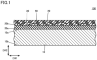
- Fig. 1 is a cross-sectional view of the superconductive wire 100.
- Fig. 2A is an enlarged view of a part in Fig. 1 .
- the superconductive wire 100 includes a substrate 10, an intermediate layer 20, a superconductive layer 30, and a plurality of precipitates 40.
- the substrate 10 has a main surface 10a and a main surface 10b.
- the main surface 10a and the main surface 10b are end surfaces in the thickness direction of the substrate 10.
- the main surface 10b is opposite to the main surface 10a.
- the substrate 10 is, for example, a cladding material composed of a tape member made of stainless steel, a copper (Cu) layer disposed on the tape member, and a nickel (Ni) layer disposed on the copper layer.
- the copper layer the copper crystal grains are crystal-oriented. Therefore, the nickel layer is also crystal-oriented along the crystal orientation of the copper layer.
- the nickel layer constitutes the main surface 10a.
- the substrate 10 may be made of Hastelloy (registered trademark).
- the substrate 10 may include a tape member made of a biaxially oriented metal material or a tape member made of a non-oriented metal material.
- the intermediate layer 20 has a main surface 20a and a main surface 20b.
- the main surface 20a and the main surface 20b are end surfaces in the thickness direction of the intermediate layer 20.
- the main surface 20b is opposite to the main surface 20a.
- the intermediate layer 20 is disposed on the main surface 10a in such a manner that the main surface 20a faces the main surface 10a.
- the intermediate layer 20 includes, for example, an yttrium oxide (Y 2 O 3 ) layer, an yttria-stabilized zirconium oxide (YSZ) layer, and a cerium oxide (CeO 2 ) layer.
- the yttrium oxide layer is disposed on the main surface 10a.
- the yttria-stabilized zirconium oxide layer is disposed on the yttrium oxide layer.
- the cerium oxide layer is disposed on the yttria-stabilized zirconium oxide layer.
- the intermediate layer 20 may not include at least one of an yttria-stabilized zirconium oxide layer and a cerium oxide layer.
- each layer of the intermediate layer 20 is crystal-oriented along the crystal orientation of the nickel layer in the substrate 10.
- the intermediate layer 20 includes, for example, an aluminum oxide (Al 2 O 3 ) layer, an yttrium oxide layer, a magnesium oxide (MgO) layer, a lanthanum manganite (LaMnO 3 ) layer, and a cerium oxide layer.
- the intermediate layer 20 may not include a cerium oxide layer.
- the superconductive layer 30 is disposed on the intermediate layer 20 (on the main surface 20b).
- the superconductive layer 30 is made of a superconductive material. More specifically, the constituent material of the superconductive layer 30 is REBa 2 Cu 3 O x (RE is a rare earth element).
- the rare earth element may be gadolinium (Gd), yttrium (Y), europium (Eu), holmium (Ho), ytterbium (Yb), samarium (Sm), dysprosium (Dy), or neodymium (Nd).
- the rare earth element is not limited thereto. Since the intermediate layer 20 is crystal-oriented as described above, the superconductive layer 30 is crystal-oriented along the crystal orientation of the intermediate layer 20. More specifically, superconductive layer 30 is crystal-oriented such that the c-axis direction of the superconductive layer 30 is along the normal direction of the main surface 20b.
- the superconductive wire 100 may further include a protective layer and a stabilization layer.
- the constituent material of the protective layer is, for example, silver or a silver alloy, and the constituent material of the stabilization layer is copper or a copper alloy.
- the protective layer is disposed on the superconductive layer 30, and the stabilization layer is disposed on the protective layer.
- the plurality of precipitates 40 are dispersed in the superconductive layer 30.
- the constituent material of the precipitate 40 is a non-superconductive material.
- the constituent material of the precipitate 40 is, for example, metal oxide.
- the constituent material of the precipitate 40 is, for example, RE 2 O 3 .
- the rare earth element contained in the constituent material of the precipitate 40 is, for example, the same as the rare earth element contained in the constituent material of the superconductive layer 30.
- the constituent material of the precipitate 40 may be BaMO 3 (M is a tetravalent metal element).
- the tetravalent metal element may be hafnium (Hf), zirconium (Zr), tin (Sn), titanium (Ti), or the like.
- the width of the precipitate 40 in the longitudinal direction is defined as a width W1.
- the cross-sectional view refers to a view where the superconductive layer 30 is observed in an arbitrary cross section orthogonal to the main surface 20b.
- the longitudinal direction of the precipitate 40 is defined as a direction in which the width of the precipitate 40 is maximum.
- the width in a direction orthogonal to the longitudinal direction of the precipitate 40 is defined as a width W2.
- the width W1 is greater than the width W2.
- an aspect ratio of the precipitate 40 is defined as value obtained by dividing the width W1 by the width W2. In the cross-sectional view, the aspect ratio of the precipitate 40 is greater than 1.
- the three-dimensional shape of the precipitate 40 may be a rod shape, a plate shape, or a disk shape.
- the average value of the aspect ratios of the plurality of precipitates 40 may be 2 or more, and may be 5 or more. In the cross-sectional view, the average value of the aspect ratios of the plurality of precipitates 40 is determined by the following method.
- a transmission electron microscope is used to acquire a TEM image of the superconductive layer 30 in an arbitrary cross section of the superconductive layer 30 orthogonal to the main surface 20b.
- the TEM image is acquired at such a magnification (a first magnification) that at least 50 precipitates 40 are present in the field of view.
- the aspect ratio of each of the plurality of precipitates 40 present in the field of view is determined by measuring the width W1 and the width W2 of each of the plurality of precipitates 40 present in the field of view. In measuring the width W1 and the width W2, the TEM image is magnified at a second magnification that is larger than the first magnification.
- a value obtained by dividing the sum of the aspect ratios of the plurality of precipitates 40 present in the observation field by the number of the plurality of precipitates 40 present in the observation field is defined as an average value of the aspect ratios of the plurality of precipitates 40 in the superconductive layer 30.
- the first magnification and the second magnification may be 50,000 times and 200,000 times, respectively.
- the minimum value of the width W1 is, for example, 10 nm or more, 20 nm or more, or 40 nm or more.
- the maximum value of the width W1 is, for example, 2000 nm or less, 1800 nm or less, or 1500 nm or less.
- the minimum value of the width W2 is, for example, 1 nm or more, 4 nm or more, or 10 nm or more.
- the maximum value of the width W2 is, for example, 200 nm or less, 150 nm or less, or 80 nm or less.
- the width W2 is as close as possible to zero at the tip portion 40c (or the tip portion 40d).
- the minimum value and the maximum value of the width W1 and the minimum value and the maximum value of the width W2 are determined by the following method. Firstly, a TEM is used to acquire a TEM image of the superconductive layer 30 in an arbitrary cross section of the superconductive layer 30 orthogonal to the main surface 20b. The TEM image is acquired at such a magnification (a first magnification) that at least 50 precipitates 40 are present in the field of view. Secondly, the width W1 is measured for each of the plurality of precipitates 40 present in the field of view. In measuring the width W1, the TEM image is magnified at a second magnification that is larger than the first magnification.
- the largest value of the measured widths W1 is defined as the maximum value of the width W1
- the smallest value of the measured widths W1 is defined as the minimum value of the width W1.
- the first magnification and the second magnification may be 50,000 times and 200,000 times, respectively.
- the minimum value and the maximum value of the width W2 are also determined by the same method.
- a direction parallel to the main surface 20b in the cross-sectional view is defined as a first direction DR1, and a direction orthogonal to the main surface 20b in the cross-sectional view is defined as a second direction DR2.
- the plurality of precipitates 40 are aligned to form a plurality of rows along the first direction DR1.
- the rows of the precipitates 40 are aligned along the first direction DR1 even if the direction in which the precipitates 40 are aligned is not parallel to the first direction DR1.
- the rows of the plurality of precipitates 40 are aligned with a spacing in the second direction DR2.
- a spacing in the first direction DR1 between two precipitates 40 adjacent to each other in the first direction DR1 is defined as a spacing SP1.
- a spacing in the second direction DR2 between two precipitates 40 adjacent to each other in the second direction DR2 is defined as a spacing SP2.
- the maximum value of the spacing SP1 is, for example, 1500 nm or less, 1000 nm or less, or 500 nm or less.
- the minimum value of the spacing SP1 is, for example, 8 nm or more, 10 nm or more, or 15 nm or more.
- the maximum value of the spacing SP2 is, for example, 500 nm or less, 400 nm or less, or 300 nm or less.
- the minimum value of the spacing SP2 is, for example, 2 nm or more, 3 nm or more, or 15 nm or more.
- the minimum value and the maximum value of the spacing SP1 and the minimum value and the maximum value of the spacing SP2 are determined by the following method. Firstly, a TEM is used to acquire a TEM image of the superconductive layer 30 in an arbitrary cross section of the superconductive layer 30 orthogonal to the main surface 20b. The TEM image is acquired at such a magnification (a first magnification) that at least 50 precipitates 40 are present in the field of view. Secondly, the spacing SP1 is measured for all of the plurality of precipitates 40 present in the field of view. In measuring the spacing SP1, the TEM image is magnified at a second magnification that is larger than the first magnification.
- the largest value of the measured spacing SP1 is defined as the maximum value of the spacing SP1 in the superconductive layer 30, and the smallest value of the measured spacing SP1 is defined as the minimum value of the spacing SP1.
- the first magnification and the second magnification may be 50,000 times and 200,000 times, respectively.
- the maximum value and the minimum value of the spacing SP2 are also determined by the same method.
- An angle formed between the longitudinal direction of the precipitate 40 and the main surface 20b in the cross-sectional view is defined as an inclination angle ⁇ 1.
- the longitudinal direction of the precipitate 40 in the cross-sectional view is defined as the direction of a straight line L1 which is defined as follows. Firstly, a straight line L2 and a straight line L3 are drawn. The straight line L2 and the straight line L3 are orthogonal to the main surface 20b and sandwich the precipitate 40. An intersection point between the straight line L2 and the precipitate 40 is defined as an intersection point P1. An intersection point between the straight line L3 and the precipitate 40 is defined as an intersection point P2.
- the straight line L1 is drawn to pass through the intersection point P1 and the intersection point P2.
- the width W1 corresponds to the length of the straight line L1.
- the inclination angle ⁇ 1 is 20° or less.
- the inclination angle ⁇ 1 may be 10° or less.
- the inclination angle ⁇ 1 is determined by the following method.
- a TEM is used to acquire a TEM image of the superconductive layer 30 in an arbitrary cross section of the superconductive layer 30 orthogonal to the main surface 20b.
- the TEM image is acquired at such a magnification (a first magnification) that at least 50 precipitates 40 are present in the field of view.
- the inclination angle ⁇ 1 is measured for each of the plurality of precipitates 40 present in the field of view.
- the TEM image is magnified at a second magnification that is larger than the first magnification.
- the first magnification and the second magnification may be 50,000 times and 200,000 times, respectively.
- both ends of the precipitate 40 in the longitudinal direction thereof are defined as an end 40a and an end 40b, respectively, and a tip portion of the end 40a in the longitudinal direction of the precipitate 40 is defined as a tip portion 40c, and a tip portion of the end 40b in the longitudinal direction of the precipitate 40 is defined as a tip portion 40d.
- the width W2 of the tip portion 40c in the direction orthogonal to the longitudinal direction of the precipitate 40 preferably becomes smaller toward the end 40a, and the width of the tip portion 40d in the direction orthogonal to the longitudinal direction of the precipitate 40 preferably becomes smaller toward the end 40b.
- the precipitate 40 may have a protruding portion 40e between the end 40a and the end 40b.
- the protruding portion 40e protrudes along a direction orthogonal to the longitudinal direction of the precipitate 40.
- Fig. 2B is an enlarged view of a part in the vicinity of an end of the precipitate 40 in the longitudinal direction.
- precipitates 41 may be further dispersed in the superconductive layer 30.
- the precipitate 41 has a granular shape.
- the precipitate 41 may have, for example, a circular shape, an oval shape, a quadrangle shape (a square shape, a rectangular shape) with rounded corners, or a shape in which those shapes are distorted (sheared) in a specific direction in the cross-sectional view.
- the precipitates 41 are aligned along the longitudinal direction of the precipitate 40 in the vicinity of an end of the precipitate 40 in the longitudinal direction thereof or in parallel with the precipitate 40, for example.
- the constituent material of the precipitate 41 is a non-superconductive material (for example, metal oxide such as RE 2 O 3 or BaMO 3 ).
- the minimum size of the precipitate 41 is, for example, 2 nm, and the maximum size of the precipitate 41 is about 16 nm.
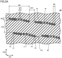
- Fig. 3A is a first enlarged cross-sectional view of a superconductive wire 100 according to a first modification.
- Fig. 3B is a second enlarged cross-sectional view of the superconductive wire 100 according to the first modification.
- precipitates 42 may be dispersed in superconductive layer 30 instead of the precipitates 40.
- the precipitates 42 may be dispersed in the superconductive layer 30 together with the precipitates 40.
- the constituent material of the precipitate 42 is a non-superconductive material (for example, metal oxide such as RE 2 O 3 or BaMO 3 ).
- the plurality of precipitates 42 are aligned in a row to form a group 43 in the cross-sectional view.
- the group 43 may include precipitates 42 in contact with each other. In other words, the group 43 may include two precipitates 42 having a spacing SP3 (which will be described later) of 0.
- a direction in which the plurality of precipitates 42 are aligned in the group 43 is defined as an alignment direction.
- a spacing in the alignment direction between two adjacent precipitates 42 of the plurality of precipitates in the group 43 is defined as a spacing SP3.
- the maximum value of the spacing SP3 is, for example, 50 nm or less, 30 nm or less, 20 nm or less, 10 nm or less, or 5 nm or less.
- the spacing SP3 may be substantially equal to 0. In other words, two adjacent precipitates 42 may be aligned substantially in contact with each other.
- the maximum value of the spacing SP3 is, for example, 1/50 or less of a spacing SP4 which will be described later.
- the maximum value of the spacing SP3 is determined by the same method as the maximum value of the spacing SP1 and the maximum value of the spacing SP2.
- the aspect ratio of the group 43 is obtained by dividing a width of the group 43 in the alignment direction by a width of the group 43 in the direction orthogonal to the alignment direction.
- the aspect ratio of the group 43 is 1 or more.
- the aspect ratio of the group 43 may be greater than 1.
- the aspect ratio of the group 43 is, for example, 3 or more or 5 or more.
- the aspect ratio of the precipitate 42 is obtained by dividing a width of the precipitate 42 in the longitudinal direction by a width of the precipitate 42 in the direction orthogonal to the longitudinal direction.
- the aspect ratio of the precipitate 42 may be, for example, 3 or less, 2 or less, or 1.5 or less.
- the precipitate 42 having an aspect ratio greater than 1 corresponds to the precipitate 40.
- the aspect ratio of the precipitate 42 may be 0.3 or more and 1 or less.
- the precipitate 42 having an aspect ratio smaller than 1 may constitute a protruding portion 43a to be described later.
- the aspect ratio of each of the plurality of precipitates 42 in the group 43 may be different from each other.
- the aspect ratio of the group 43 and the aspect ratio of the precipitate 42 are determined by the same method as the aspect ratio of the precipitate 40.
- the width of the group 43 in the alignment direction thereof is defined as a width W3
- the width of the group 43 in a direction orthogonal to the alignment direction thereof is defined as a width W4
- the width of the precipitate 42 in the alignment direction of the group 43 is defined as a width W5.
- the minimum value of the width W3 is, for example, 10 nm or more, 20 nm or more, or 30 nm or more.
- the maximum value of the width W3 is, for example, 10000 nm or less, 1700 nm or less, or 900 nm or less.
- the minimum value of the width W4 is, for example, 1 nm or more, 2 nm or more, or 3 nm or more.
- the maximum value of the width W4 is, for example, 200 nm or less, 150 nm or less, 100 nm or less, or 80 nm or less.
- the minimum value of the width W5 is, for example, 1 nm or more.
- the maximum value of the width W5 is, for example, 100 nm or less, 60 nm or less, or 40 nm or less.
- the alignment direction is defined as the direction of a straight line L4 which is defined as follows. Firstly, a straight line L5 and a straight line L6 are drawn. The straight line L5 and the straight line L6 are orthogonal to the main surface 20b and sandwich the group 43. An intersection point between the straight line L5 and the precipitate 42 at the first end of the group 43 is defined as an intersection point P3. An intersection point between the straight line L6 and the precipitate 42 at the second end (the end opposite to the first end) of the group 43 is defined as an intersection point P4. The straight line L4 is drawn to pass through the intersection point P3 and the intersection point P4. The inclination angle ⁇ 2 is 20° or less. The inclination angle ⁇ 2 is determined by the same method as the inclination angle ⁇ 1.
- a spacing between two groups 43 adjacent to each other in the first direction DR1 is defined as a spacing SP4
- a spacing between two groups 43 adjacent to each other in the second direction DR2 is defined as a spacing SP5.
- the maximum value of the spacing SP4 is, for example, 2500 nm or less.
- the minimum value of the spacing SP4 is, for example, 2 nm or more.
- the maximum value of the spacing SP5 is, for example, 2000 nm or less.
- the minimum value of the spacing SP5 is, for example, 1 nm or more.
- the maximum value and the minimum value of the spacing SP4 are determined in the same manner as the maximum value and the minimum value of the spacing SP1, and the maximum value and the minimum value of the spacing SP5 are determined in the same manner as the maximum value and the minimum value of the spacing SP2.
- Fig. 4 is an enlarged cross-sectional view of a superconductive wire 100 according to a second modification.
- the longitudinal direction of a precipitate 42 may intersect the alignment direction.
- the group 43 may have, between both ends thereof in the alignment direction, a protruding portion 43a that protrudes along a direction orthogonal to the alignment direction.
- the protruding portion 43a may be a part of the precipitates 42 in the group 43, and the aspect ratio of the precipitates 42 included in the part is smaller than the aspect ratio of the other precipitates 42 in the group.
- Fig. 5 is an enlarged cross-sectional view of a superconductive wire 100 according to a third modification. As illustrated in Fig. 5 , the precipitates 41 are not aligned along the longitudinal direction of the precipitate 40, but are evenly dispersed throughout the superconductive layer 30.
- Fig. 6 is an enlarged cross-sectional view of a superconductive wire 100 according to a fourth modification.
- precipitates 44 may be further dispersed in the superconductive layer 30.
- the constituent material of the precipitate 44 is a non-superconductive material (for example, metal oxide such as RE 2 O 3 or BaMO 3 ).
- the aspect ratio of the precipitate 44 is obtained by dividing the width in the longitudinal direction of the precipitate 44 by the width in the direction orthogonal to the longitudinal direction of the precipitate 44 in the cross-sectional view.
- the aspect ratio of the precipitate 44 is greater than 1.
- the angle formed between the longitudinal direction of the precipitate 44 and the main surface 20b is, for example, 60° or more.
- Fig. 7 is an enlarged cross-sectional view of a superconductive wire 100 according to a fifth modification.
- a plurality of precipitates 45 may be further dispersed in the superconductive layer 30.
- the constituent material of the precipitate 45 is a non-superconductive material (for example, metal oxide such as RE 2 O 3 or BaMO 3 ).
- the plurality of precipitates 45 are aligned in a row to form a group 46 in the cross-sectional view.
- the angle formed between the direction in which the precipitates 45 are aligned in the group 46 and the main surface 20b is 60° or more.
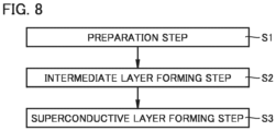
- Fig. 8 is a process chart of manufacturing a superconductive wire 100.
- the method of manufacturing a superconductive wire 100 includes a preparation step S1, an intermediate layer forming step S2, and a superconductive layer forming step S3.
- the intermediate layer forming step S2 is performed after the preparation step S1.
- the superconductive layer forming step S3 is performed after the intermediate layer forming step S2.
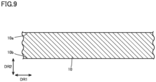
- Fig. 9 is a cross-sectional view illustrating the preparation step S1.
- a substrate 10 is prepared.
- an intermediate layer 20 is not disposed on the main surface 10a.
- Fig. 10 is a cross-sectional view illustrating the intermediate layer forming step S2.
- the intermediate layer 20 in which crystals are oriented is formed on the main surface 10a.
- the intermediate layer 20 is formed by sequentially forming each layer that constitutes the intermediate layer 20 by, for example, a magnetron sputtering method, an ion beam sputtering method, or a PLD (Pulsed Laser Deposition) method.
- Fig. 11 is a cross-sectional view illustrating the superconductive layer forming step S3.
- a superconductive layer 31 is formed on the intermediate layer 20.
- the superconductive layer 31 is thinner than the superconductive layer 30.
- the superconductive layer 31 is formed by, for example, a MOD (Metal Organic Decomposition) method, a MOCVD (Metal Organic Chemical Vapor Deposition) method, or a PLD method.
- the precipitates 40 are deposited on the surface or the inside of the superconductive layer 31 by shifting the rare earth element from the stoichiometric composition.
- another superconductive layer 31 is formed on the already formed superconductive layer 31 in a similar manner. This process is repeated to form a plurality of superconductive layers 31 constituting the superconductive layer 30, and thereby, the superconductive wire 100 having the structure illustrated in Figs. 1 and 2A is manufactured.
- the precipitates 40, the precipitates 41, and the precipitates 42 are deposited on the surface or the inside of the superconductive layer 31 by repeatedly stacking the superconductive layers in the superconductive layer forming step S3.
- a superconductive wire according to a first comparative example and a superconductive wire according to a second comparative example are defined as a superconductive wire 100A and a superconductive wire 100B, respectively.
- the configuration of the superconductive wire 100A is different from the configuration of the superconductive wire 100 in that precipitates 40 are not dispersed in the superconductive layer 30.
- the superconductive wire 100B granular precipitates are dispersed in the superconductive layer 30.
- the precipitate is BaZr 2 O 3 and functions as a magnetic flux pin.
- the configuration of the superconductive wire 100B is different from the configuration of the superconductive wire 100.
- Samples 1 to 6 were prepared as the superconductive wire samples. Sample 1 and Sample 2 correspond to the superconductive wire 100A and the superconductive wire 100B, respectively. Each of samples 3 to 6 correspond to the superconductive wire 100.
- the type of the precipitates precipitate 40 as the first precipitate and precipitate 42 as the second precipitate
- the aspect ratio of the precipitate 40 the average value of the aspect ratio of the precipitate 40
- the inclination angle ⁇ 1 or the inclination angle ⁇ 2 the width W1 to the width W5, and the spacing SP1 to the spacing SP5 were changed.
- the numerical range in Table 1 shows the determination results of the widths or angles for 10 or more precipitates observed from the field of view set as described above.
- the width W1 of Sample 4 was in the range of 10 nm or more and 350 nm or less.
- the average value of the inclination angle ⁇ 1, the inclination angle ⁇ 2, and the aspect ratio of the precipitate 40 is an average value for 10 or more precipitates.
- no precipitate was observed.
- the precipitate 42 was observed, and in Sample 4, the precipitate 40 and the precipitate 42 were observed.
- Sample 5 the precipitate 40 was observed.
- Sample 6 the precipitate 42 was observed.
- the group 43 of the precipitates 42 had a protruding portion 43a, and the precipitate 40 had a tip portion 40c (or a tip portion 40d), the width W2 of which becomes smaller toward the end 40a (or the end 40b), and the precipitate 41 was observed.
- the precipitate 40 had a protruding portion 40e, and the precipitate 40 had a tip portion 40c (or a tip portion 40d), the width W2 of which becomes smaller toward the end 40a (the end 40b), and the precipitate 41 was observed.
- the group 43 of the precipitates 42 had a protruding portion 43a.
- Jc Jc of each superconductive wire under a self-magnetic field at 77 K and Jc of each superconductive wire under a 3T magnetic field at 30 K were measured.
- the 3T magnetic field was applied in a direction perpendicular to the main surface 20b.
- Jc represents a critical current density.
- Table 2 The value of ⁇ is calculated for each superconductive wire by dividing Jc measured under a 3T magnetic field at 30 K by Jc measured under a self-magnetic field at 77 K, and serves as an index of the low-temperature magnetic field property. The larger the value of ⁇ is, the better the low-temperature magnetic field property is.
- Jc was calculated from a critical current value (Ic) measured from each sample when the thickness of the superconductive layer 30 was 3 ⁇ 0.5 ⁇ m and the width of the superconductive layer 30 was 4 mm.
- the value of ⁇ for Samples 3 to 6 was larger than the value of ⁇ for Samples 1 and 2.
- at least one of the following conditions was satisfied: (a) the aspect ratio of the precipitate 40 is greater than 1 and the inclination angle ⁇ 1 is 20° or less; and (b) the precipitates 42 are aligned in a row to form a group 43 and the inclination angle ⁇ 2 is 20° or less. From this comparison, it was experimentally evident that the low-temperature magnetic field property of the superconductive wire 100 is improved when conditions (a) and (b) are satisfied.
- the value of ⁇ was highest in sample 4 where both the precipitates 40 and the group 43 of the precipitates 42 were present in the superconductive layer 30. Therefore, it was experimentally evident that the low-temperature magnetic field property is further improved by the presence of both the precipitates 40 and the group 43 of the precipitates 42 in the superconductive layer 30.
- both ends of the precipitate 40 in the longitudinal direction function as magnetic flux pins for improving the low-temperature magnetic field property. Therefore, when the aspect ratio of the precipitate 40 becomes greater than 1, the portions functioning as the magnetic flux pins in the superconductive layer 30 can be regarded as being dispersed at intervals, and thereby the low-temperature magnetic field property of the superconductive wire 100 is improved as compared with the superconductive wire 100A and the superconductive wire 100B.
- the spacing SP1 is, the more likely for the precipitate 40 to function as a magnetic flux pin, by setting the maximum value of the spacing SP1 to 1500 nm or less, the low-temperature magnetic field property of the superconductive wire 100 is further improved. Since it is considered that the smaller the spacing SP2 is, the more likely for the precipitate 40 to function as a magnetic flux pin, by setting the maximum value of the spacing SP2 to 500 nm or less, the low-temperature magnetic field property of the superconductive wire 100 is further improved.
- the portions of the precipitate 40 functioning as the magnetic flux pins are appropriately dispersed, and thereby the low-temperature magnetic field property of the superconductive wire 100 is further improved.
- the tip portion 40c (or the tip portion 40d) in the direction orthogonal to the longitudinal direction of the precipitate 40 becomes smaller toward the end 40a (or the end 40b), it is considered that the tip portion 40c (or the tip portion 40d) is more likely to function as a magnetic flux pin, and thereby the low-temperature magnetic field property of the superconductive wire 100 is further improved.
- the precipitate 40 has a protruding portion 40e (the group 43 has a protruding portion 43a)
- the protruding portion 40e is more likely to function as a magnetic flux pin, and thereby the low-temperature magnetic field property of the superconductive wire 100 is further improved.
Landscapes
- Engineering & Computer Science (AREA)
- Chemical & Material Sciences (AREA)
- Ceramic Engineering (AREA)
- Superconductors And Manufacturing Methods Therefor (AREA)
- Manufacturing & Machinery (AREA)
Abstract
Description
- The present disclosure relates to a superconductive wire. The present application claims the benefit of priority to
Japanese Patent Application No. 2022-198562 filed on December 13, 2022 - For example,
WO 2017/217487 (PTL 1) describes a superconductive wire. The superconductive wire described inPTL 1 includes a substrate, an intermediate layer, a superconductive layer, and a plurality of artificial pin rods. - The substrate has a first main surface. The intermediate layer has a second main surface and a third main surface opposite to the second main surface. The intermediate layer is disposed on the substrate in such a manner that the second main surface faces the first main surface. The superconductive layer is disposed on the third main surface. The plurality of artificial pin rods are dispersed in the superconductive layer.
- The constituent material of the superconductive layer is REBa2Cu3Ox (RE is a rare earth element). The constituent material of each of the plurality of artificial pin rods is RE2O3 or BaMO3 (M is a tetravalent metal element). The c-axis direction of the superconductive layer is along the normal direction of the third main surface. The longitudinal direction of the artificial pin rod is along the c-axis direction of the superconductive layer.
- PTL 1:
WO 2017/217487 - A superconductive wire of the present disclosure includes a substrate, an intermediate layer, a superconductive layer, a plurality of first precipitates and/or a plurality of second precipitates. The substrate has a first main surface. The intermediate layer has a second main surface and a third main surface opposite to the second main surface, and is disposed on the substrate in such a manner that the second main surface faces the first main surface. The superconductive layer is disposed on the third main surface. The constituent material of the superconductive layer is REBa2Cu3Ox (RE is a rare earth element). The plurality of first precipitates and the plurality of second precipitates are dispersed in the superconductive layer. The constituent material of each of the plurality of first precipitates and the constituent material of each of the plurality of second precipitates are non-superconductive material. In a cross-sectional view orthogonal to the third main surface, an aspect ratio of each of the plurality of first precipitates is greater than 1. In the cross-sectional view, the longitudinal direction of each of the plurality of first precipitates forms an angle of 20° or less with respect to the third main surface. In the cross-sectional view, the plurality of second precipitates are aligned in a row to form a group. In the cross-sectional view, an alignment direction of the plurality of second precipitates in the group forms an angle of 20° or less with respect to the third main surface.
-
-
Fig. 1 is a cross-sectional view of asuperconductive wire 100; -
Fig. 2A is an enlarged view of a part inFig. 1 ; -
Fig. 2B is an enlarged view of a part in the vicinity of an end of a precipitate 40 in the longitudinal direction; -
Fig. 3A is a first enlarged cross-sectional view of asuperconductive wire 100 according to a first modification; -
Fig. 3B is a second enlarged cross-sectional view of thesuperconductive wire 100 according to the first modification; -
Fig. 4 is an enlarged cross-sectional view of asuperconductive wire 100 according to a second modification; -
Fig. 5 is an enlarged cross-sectional view of asuperconductive wire 100 according to a third modification; -
Fig. 6 is an enlarged cross-sectional view of asuperconductive wire 100 according to a fourth modification; -
Fig. 7 is an enlarged cross-sectional view of asuperconductive wire 100 according to a fifth modification; -
Fig. 8 is a process chart of manufacturing thesuperconductive wire 100; -
Fig. 9 is a cross-sectional view illustrating a preparation step S1; -
Fig. 10 is a cross-sectional view illustrating the intermediate layer forming step S2; and -
Fig. 11 is a cross-sectional view illustrating a superconductive layer forming step S3. - The superconductive wire described in
PTL 1 has a room for improvement in low-temperature magnetic field property. The present disclosure has been made in view of the above-mentioned problem in the prior arts. More specifically, the present disclosure provides a superconductive wire with an improved low-temperature magnetic field property. - According to the superconductive wire of the present disclosure, the low-temperature magnetic field property can be improved.
- First, embodiments of the present disclosure will be described.
- (1) A superconductive wire according to an embodiment includes a substrate, an intermediate layer, a superconductive layer, a plurality of first precipitates and/or a plurality of second precipitates. The substrate has a first main surface. The intermediate layer has a second main surface and a third main surface opposite to the second main surface, and is disposed on the substrate in such a manner that the second main surface faces the first main surface. The superconductive layer is disposed on the third main surface. The constituent material of the superconductive layer is REBa2Cu3Ox (RE is a rare earth element). The plurality of first precipitates and the plurality of second precipitates are dispersed in the superconductive layer. The constituent material of each of the plurality of first precipitates and the constituent material of each of the plurality of second precipitates are non-superconductive material. In a cross-sectional view orthogonal to the third main surface, an aspect ratio of each of the plurality of first precipitates is greater than 1. In the cross-sectional view, the longitudinal direction of each of the plurality of first precipitates forms an angle of 20° or less with respect to the third main surface. In the cross-sectional view, the plurality of second precipitates are aligned in a row to form a group. In the cross-sectional view, an alignment direction of the plurality of second precipitates in the group forms an angle of 20° or less with respect to the third main surface.
According to the superconductive wire of the above (1), the low-temperature magnetic field property can be improved. - (2) In the superconductive wire of the above (1), the constituent material of each of the plurality of first precipitates may be metal oxide.
- (3) In the superconductive wire of the above (1) or (2), the constituent material of each of the plurality of first precipitates may be RE2O3 or BaMO3 (M is a tetravalent metal element).
- (4) In the superconductive wire of the above (1) to (3), the average value of the aspect ratios of the plurality of first precipitates may be 2 or more.
- (5) In the superconductive wire of the above (1) to (4), a third precipitate may be further dispersed in the superconductive layer. The constituent material of the third precipitate may be a non-superconductive material. In the cross-sectional view, the third precipitate may have a granular shape.
According to the superconductive wire of the above (5), the low-temperature magnetic field property can be further improved. - (6) In the superconductive wire of the above (1) to (5), in the cross-sectional view, the maximum value of a spacing in the direction parallel to the third main surface between two adjacent precipitates of the plurality of first precipitates in the direction parallel to the third main surface may be 1500 nm or less.
According to the superconductive wire of the above (6), the low-temperature magnetic field property can be further improved. - (7) In the superconductive wire of the above (1) to (6), in the cross-sectional view, the maximum value of a spacing in the direction orthogonal to the third main surface between two adjacent precipitates of the plurality of first precipitates in the direction orthogonal to the third main surface may be 500 nm or less.
According to the superconductive wire of the above (7), the low-temperature magnetic field property can be further improved. - (8) In the superconductive wire of the above (1) to (7), in the cross-sectional view, the minimum value and the maximum value of a width in the longitudinal direction of each of the plurality of first precipitates may be 10 nm or more and 2000 nm or less, respectively.
According to the superconductive wire of the above (8), the low-temperature magnetic field property can be further improved. - (9) In the superconductive wire of the above (1) to (8), in the cross-sectional view, the maximum value of the width in the direction orthogonal to the longitudinal direction of each of the plurality of first precipitates may be 200 nm or less.
According to the superconductive wire of the above (9), the low-temperature magnetic field property can be further improved. - (10) In the superconductive wire of the above (1) to (9), in the cross-sectional view, at least one of the plurality of first precipitates may have, between both ends thereof in the longitudinal direction, a first protruding portion that protrudes along a direction orthogonal to the longitudinal direction. In the cross-sectional view, the group may have, between both ends thereof in the alignment direction, a second protruding portion that protrudes along a direction orthogonal to the alignment direction.
According to the superconductive wire of the above (10), the low-temperature magnetic field property can be further improved. - (11) In the superconductive wire of the above (1) to (10), each of the plurality of first precipitates may a tip portion at an end in the longitudinal direction, and the width of the tip portion in a direction orthogonal to the longitudinal direction becomes smaller toward the end.
- According to the superconductive wire of the above (11), the low-temperature magnetic field property can be further improved.
- Next, embodiments of the present disclosure will be described in detail with reference to the drawings. In the following drawings, the same or corresponding parts are denoted by the same reference numerals, and the description thereof will not be repeated. The superconductive wire according to the embodiment is defined as a
superconductive wire 100. - Hereinafter, the configuration of a
superconductive wire 100 will be described. -
Fig. 1 is a cross-sectional view of thesuperconductive wire 100.Fig. 2A is an enlarged view of a part inFig. 1 . As illustrated inFigs. 1 and2A , thesuperconductive wire 100 includes asubstrate 10, anintermediate layer 20, asuperconductive layer 30, and a plurality ofprecipitates 40. - The
substrate 10 has amain surface 10a and amain surface 10b. Themain surface 10a and themain surface 10b are end surfaces in the thickness direction of thesubstrate 10. Themain surface 10b is opposite to themain surface 10a. - The
substrate 10 is, for example, a cladding material composed of a tape member made of stainless steel, a copper (Cu) layer disposed on the tape member, and a nickel (Ni) layer disposed on the copper layer. In the copper layer, the copper crystal grains are crystal-oriented. Therefore, the nickel layer is also crystal-oriented along the crystal orientation of the copper layer. The nickel layer constitutes themain surface 10a. Thesubstrate 10 may be made of Hastelloy (registered trademark). Thesubstrate 10 may include a tape member made of a biaxially oriented metal material or a tape member made of a non-oriented metal material. - The
intermediate layer 20 has amain surface 20a and amain surface 20b. Themain surface 20a and themain surface 20b are end surfaces in the thickness direction of theintermediate layer 20. Themain surface 20b is opposite to themain surface 20a. Theintermediate layer 20 is disposed on themain surface 10a in such a manner that themain surface 20a faces themain surface 10a. - The
intermediate layer 20 includes, for example, an yttrium oxide (Y2O3) layer, an yttria-stabilized zirconium oxide (YSZ) layer, and a cerium oxide (CeO2) layer. The yttrium oxide layer is disposed on themain surface 10a. The yttria-stabilized zirconium oxide layer is disposed on the yttrium oxide layer. The cerium oxide layer is disposed on the yttria-stabilized zirconium oxide layer. Theintermediate layer 20 may not include at least one of an yttria-stabilized zirconium oxide layer and a cerium oxide layer. As described above, since the nickel layer of thesubstrate 10 is crystal-oriented, each layer of theintermediate layer 20 is crystal-oriented along the crystal orientation of the nickel layer in thesubstrate 10. When thesubstrate 10 is made of Hastelloy (registered trademark), theintermediate layer 20 includes, for example, an aluminum oxide (Al2O3) layer, an yttrium oxide layer, a magnesium oxide (MgO) layer, a lanthanum manganite (LaMnO3) layer, and a cerium oxide layer. In this case, theintermediate layer 20 may not include a cerium oxide layer. - The
superconductive layer 30 is disposed on the intermediate layer 20 (on themain surface 20b). Thesuperconductive layer 30 is made of a superconductive material. More specifically, the constituent material of thesuperconductive layer 30 is REBa2Cu3Ox (RE is a rare earth element). The rare earth element may be gadolinium (Gd), yttrium (Y), europium (Eu), holmium (Ho), ytterbium (Yb), samarium (Sm), dysprosium (Dy), or neodymium (Nd). The rare earth element is not limited thereto. Since theintermediate layer 20 is crystal-oriented as described above, thesuperconductive layer 30 is crystal-oriented along the crystal orientation of theintermediate layer 20. More specifically,superconductive layer 30 is crystal-oriented such that the c-axis direction of thesuperconductive layer 30 is along the normal direction of themain surface 20b. - Although not shown in the figures, the
superconductive wire 100 may further include a protective layer and a stabilization layer. The constituent material of the protective layer is, for example, silver or a silver alloy, and the constituent material of the stabilization layer is copper or a copper alloy. The protective layer is disposed on thesuperconductive layer 30, and the stabilization layer is disposed on the protective layer. - The plurality of
precipitates 40 are dispersed in thesuperconductive layer 30. The constituent material of the precipitate 40 is a non-superconductive material. The constituent material of the precipitate 40 is, for example, metal oxide. The constituent material of the precipitate 40 is, for example, RE2O3. The rare earth element contained in the constituent material of the precipitate 40 is, for example, the same as the rare earth element contained in the constituent material of thesuperconductive layer 30. The constituent material of the precipitate 40 may be BaMO3 (M is a tetravalent metal element). The tetravalent metal element may be hafnium (Hf), zirconium (Zr), tin (Sn), titanium (Ti), or the like. - In the cross-sectional view, the width of the precipitate 40 in the longitudinal direction is defined as a width W1. The cross-sectional view refers to a view where the
superconductive layer 30 is observed in an arbitrary cross section orthogonal to themain surface 20b. The longitudinal direction of the precipitate 40 is defined as a direction in which the width of the precipitate 40 is maximum. In the cross-sectional view, the width in a direction orthogonal to the longitudinal direction of the precipitate 40 is defined as a width W2. The width W1 is greater than the width W2. - In the cross-sectional view, an aspect ratio of the precipitate 40 is defined as value obtained by dividing the width W1 by the width W2. In the cross-sectional view, the aspect ratio of the precipitate 40 is greater than 1. The three-dimensional shape of the precipitate 40 may be a rod shape, a plate shape, or a disk shape. In the cross-sectional view, the average value of the aspect ratios of the plurality of
precipitates 40 may be 2 or more, and may be 5 or more. In the cross-sectional view, the average value of the aspect ratios of the plurality ofprecipitates 40 is determined by the following method. - Firstly, a transmission electron microscope (TEM) is used to acquire a TEM image of the
superconductive layer 30 in an arbitrary cross section of thesuperconductive layer 30 orthogonal to themain surface 20b. The TEM image is acquired at such a magnification (a first magnification) that at least 50 precipitates 40 are present in the field of view. Secondly, the aspect ratio of each of the plurality ofprecipitates 40 present in the field of view is determined by measuring the width W1 and the width W2 of each of the plurality ofprecipitates 40 present in the field of view. In measuring the width W1 and the width W2, the TEM image is magnified at a second magnification that is larger than the first magnification. Thirdly, a value obtained by dividing the sum of the aspect ratios of the plurality ofprecipitates 40 present in the observation field by the number of the plurality ofprecipitates 40 present in the observation field is defined as an average value of the aspect ratios of the plurality ofprecipitates 40 in thesuperconductive layer 30. The first magnification and the second magnification may be 50,000 times and 200,000 times, respectively. - The minimum value of the width W1 is, for example, 10 nm or more, 20 nm or more, or 40 nm or more. The maximum value of the width W1 is, for example, 2000 nm or less, 1800 nm or less, or 1500 nm or less. The minimum value of the width W2 is, for example, 1 nm or more, 4 nm or more, or 10 nm or more. The maximum value of the width W2 is, for example, 200 nm or less, 150 nm or less, or 80 nm or less. As illustrated in
Fig. 2A , in a precipitate 40 having atip portion 40c (or atip portion 40d) with a smaller width W2, the width W2 is as close as possible to zero at thetip portion 40c (or thetip portion 40d). - The minimum value and the maximum value of the width W1 and the minimum value and the maximum value of the width W2 are determined by the following method. Firstly, a TEM is used to acquire a TEM image of the
superconductive layer 30 in an arbitrary cross section of thesuperconductive layer 30 orthogonal to themain surface 20b. The TEM image is acquired at such a magnification (a first magnification) that at least 50 precipitates 40 are present in the field of view. Secondly, the width W1 is measured for each of the plurality ofprecipitates 40 present in the field of view. In measuring the width W1, the TEM image is magnified at a second magnification that is larger than the first magnification. Thirdly, the largest value of the measured widths W1 is defined as the maximum value of the width W1, and the smallest value of the measured widths W1 is defined as the minimum value of the width W1. The first magnification and the second magnification may be 50,000 times and 200,000 times, respectively. The minimum value and the maximum value of the width W2 are also determined by the same method. - A direction parallel to the
main surface 20b in the cross-sectional view is defined as a first direction DR1, and a direction orthogonal to themain surface 20b in the cross-sectional view is defined as a second direction DR2. In the cross-sectional view, the plurality ofprecipitates 40 are aligned to form a plurality of rows along the first direction DR1. The rows of theprecipitates 40 are aligned along the first direction DR1 even if the direction in which theprecipitates 40 are aligned is not parallel to the first direction DR1. The rows of the plurality ofprecipitates 40 are aligned with a spacing in the second direction DR2. - A spacing in the first direction DR1 between two
precipitates 40 adjacent to each other in the first direction DR1 is defined as a spacing SP1. A spacing in the second direction DR2 between twoprecipitates 40 adjacent to each other in the second direction DR2 is defined as a spacing SP2. - The maximum value of the spacing SP1 is, for example, 1500 nm or less, 1000 nm or less, or 500 nm or less. The minimum value of the spacing SP1 is, for example, 8 nm or more, 10 nm or more, or 15 nm or more. The maximum value of the spacing SP2 is, for example, 500 nm or less, 400 nm or less, or 300 nm or less. The minimum value of the spacing SP2 is, for example, 2 nm or more, 3 nm or more, or 15 nm or more.
- The minimum value and the maximum value of the spacing SP1 and the minimum value and the maximum value of the spacing SP2 are determined by the following method. Firstly, a TEM is used to acquire a TEM image of the
superconductive layer 30 in an arbitrary cross section of thesuperconductive layer 30 orthogonal to themain surface 20b. The TEM image is acquired at such a magnification (a first magnification) that at least 50 precipitates 40 are present in the field of view. Secondly, the spacing SP1 is measured for all of the plurality ofprecipitates 40 present in the field of view. In measuring the spacing SP1, the TEM image is magnified at a second magnification that is larger than the first magnification. Thirdly, the largest value of the measured spacing SP1 is defined as the maximum value of the spacing SP1 in thesuperconductive layer 30, and the smallest value of the measured spacing SP1 is defined as the minimum value of the spacing SP1. The first magnification and the second magnification may be 50,000 times and 200,000 times, respectively. The maximum value and the minimum value of the spacing SP2 are also determined by the same method. - An angle formed between the longitudinal direction of the precipitate 40 and the
main surface 20b in the cross-sectional view is defined as an inclination angle Θ1. The longitudinal direction of the precipitate 40 in the cross-sectional view is defined as the direction of a straight line L1 which is defined as follows. Firstly, a straight line L2 and a straight line L3 are drawn. The straight line L2 and the straight line L3 are orthogonal to themain surface 20b and sandwich the precipitate 40. An intersection point between the straight line L2 and the precipitate 40 is defined as an intersection point P1. An intersection point between the straight line L3 and the precipitate 40 is defined as an intersection point P2. The straight line L1 is drawn to pass through the intersection point P1 and the intersection point P2. The width W1 corresponds to the length of the straight line L1. The inclination angle θ1 is 20° or less. The inclination angle θ1 may be 10° or less. The inclination angle θ1 is determined by the following method. - Firstly, a TEM is used to acquire a TEM image of the
superconductive layer 30 in an arbitrary cross section of thesuperconductive layer 30 orthogonal to themain surface 20b. The TEM image is acquired at such a magnification (a first magnification) that at least 50 precipitates 40 are present in the field of view. Secondly, the inclination angle θ1 is measured for each of the plurality ofprecipitates 40 present in the field of view. In measuring the inclination angle θ1 , the TEM image is magnified at a second magnification that is larger than the first magnification. Thus, if the inclination angle θ1 is 20° or less for all of the plurality ofprecipitates 40 present in the field of view, the relationship that "the inclination angle θ1 is 20° or less" is satisfied. The first magnification and the second magnification may be 50,000 times and 200,000 times, respectively. - In the cross-sectional view, both ends of the precipitate 40 in the longitudinal direction thereof are defined as an
end 40a and anend 40b, respectively, and a tip portion of theend 40a in the longitudinal direction of the precipitate 40 is defined as atip portion 40c, and a tip portion of theend 40b in the longitudinal direction of the precipitate 40 is defined as atip portion 40d. The width W2 of thetip portion 40c in the direction orthogonal to the longitudinal direction of the precipitate 40 preferably becomes smaller toward theend 40a, and the width of thetip portion 40d in the direction orthogonal to the longitudinal direction of the precipitate 40 preferably becomes smaller toward theend 40b. - In the cross-sectional view, the precipitate 40 may have a protruding
portion 40e between theend 40a and theend 40b. In the cross-sectional view, the protrudingportion 40e protrudes along a direction orthogonal to the longitudinal direction of the precipitate 40. -
Fig. 2B is an enlarged view of a part in the vicinity of an end of the precipitate 40 in the longitudinal direction. As illustrated inFig. 2B , precipitates 41 may be further dispersed in thesuperconductive layer 30. In the cross-sectional view, the precipitate 41 has a granular shape. In the cross-sectional view, the precipitate 41 may have, for example, a circular shape, an oval shape, a quadrangle shape (a square shape, a rectangular shape) with rounded corners, or a shape in which those shapes are distorted (sheared) in a specific direction in the cross-sectional view. Theprecipitates 41 are aligned along the longitudinal direction of the precipitate 40 in the vicinity of an end of the precipitate 40 in the longitudinal direction thereof or in parallel with the precipitate 40, for example. The constituent material of the precipitate 41 is a non-superconductive material (for example, metal oxide such as RE2O3 or BaMO3). The minimum size of the precipitate 41 is, for example, 2 nm, and the maximum size of the precipitate 41 is about 16 nm. -
Fig. 3A is a first enlarged cross-sectional view of asuperconductive wire 100 according to a first modification.Fig. 3B is a second enlarged cross-sectional view of thesuperconductive wire 100 according to the first modification. As illustrated inFig. 3A , precipitates 42 may be dispersed insuperconductive layer 30 instead of theprecipitates 40. As illustrated inFig. 3B , theprecipitates 42 may be dispersed in thesuperconductive layer 30 together with theprecipitates 40. The constituent material of the precipitate 42 is a non-superconductive material (for example, metal oxide such as RE2O3 or BaMO3). The plurality ofprecipitates 42 are aligned in a row to form agroup 43 in the cross-sectional view. There may be a plurality ofgroups 43 in thesuperconductive layer 30. Thegroup 43 may includeprecipitates 42 in contact with each other. In other words, thegroup 43 may include twoprecipitates 42 having a spacing SP3 (which will be described later) of 0. - In the cross-sectional view, a direction in which the plurality of
precipitates 42 are aligned in thegroup 43 is defined as an alignment direction. A spacing in the alignment direction between twoadjacent precipitates 42 of the plurality of precipitates in thegroup 43 is defined as a spacing SP3. The maximum value of the spacing SP3 is, for example, 50 nm or less, 30 nm or less, 20 nm or less, 10 nm or less, or 5 nm or less. The spacing SP3 may be substantially equal to 0. In other words, twoadjacent precipitates 42 may be aligned substantially in contact with each other. The maximum value of the spacing SP3 is, for example, 1/50 or less of a spacing SP4 which will be described later. The maximum value of the spacing SP3 is determined by the same method as the maximum value of the spacing SP1 and the maximum value of the spacing SP2. - In the cross-sectional view, the aspect ratio of the
group 43 is obtained by dividing a width of thegroup 43 in the alignment direction by a width of thegroup 43 in the direction orthogonal to the alignment direction. The aspect ratio of thegroup 43 is 1 or more. The aspect ratio of thegroup 43 may be greater than 1. The aspect ratio of thegroup 43 is, for example, 3 or more or 5 or more. The aspect ratio of the precipitate 42 is obtained by dividing a width of the precipitate 42 in the longitudinal direction by a width of the precipitate 42 in the direction orthogonal to the longitudinal direction. The aspect ratio of the precipitate 42 may be, for example, 3 or less, 2 or less, or 1.5 or less. The precipitate 42 having an aspect ratio greater than 1 corresponds to the precipitate 40. The aspect ratio of the precipitate 42 may be 0.3 or more and 1 or less. The precipitate 42 having an aspect ratio smaller than 1 may constitute a protrudingportion 43a to be described later. The aspect ratio of each of the plurality ofprecipitates 42 in thegroup 43 may be different from each other. The aspect ratio of thegroup 43 and the aspect ratio of the precipitate 42 are determined by the same method as the aspect ratio of the precipitate 40. - In the cross-sectional view, the width of the
group 43 in the alignment direction thereof is defined as a width W3, the width of thegroup 43 in a direction orthogonal to the alignment direction thereof is defined as a width W4, and the width of the precipitate 42 in the alignment direction of thegroup 43 is defined as a width W5. The minimum value of the width W3 is, for example, 10 nm or more, 20 nm or more, or 30 nm or more. The maximum value of the width W3 is, for example, 10000 nm or less, 1700 nm or less, or 900 nm or less. The minimum value of the width W4 is, for example, 1 nm or more, 2 nm or more, or 3 nm or more. The maximum value of the width W4 is, for example, 200 nm or less, 150 nm or less, 100 nm or less, or 80 nm or less. The minimum value of the width W5 is, for example, 1 nm or more. The maximum value of the width W5 is, for example, 100 nm or less, 60 nm or less, or 40 nm or less. - An angle formed between the alignment direction and the
main surface 20b in the cross-sectional view is defined as an inclination angle Θ2. The alignment direction is defined as the direction of a straight line L4 which is defined as follows. Firstly, a straight line L5 and a straight line L6 are drawn. The straight line L5 and the straight line L6 are orthogonal to themain surface 20b and sandwich thegroup 43. An intersection point between the straight line L5 and the precipitate 42 at the first end of thegroup 43 is defined as an intersection point P3. An intersection point between the straight line L6 and the precipitate 42 at the second end (the end opposite to the first end) of thegroup 43 is defined as an intersection point P4. The straight line L4 is drawn to pass through the intersection point P3 and the intersection point P4. The inclination angle Θ2 is 20° or less. The inclination angle Θ2 is determined by the same method as the inclination angle Θ1. - In the cross-sectional view, a spacing between two
groups 43 adjacent to each other in the first direction DR1 is defined as a spacing SP4, and a spacing between twogroups 43 adjacent to each other in the second direction DR2 is defined as a spacing SP5. The maximum value of the spacing SP4 is, for example, 2500 nm or less. The minimum value of the spacing SP4 is, for example, 2 nm or more. The maximum value of the spacing SP5 is, for example, 2000 nm or less. The minimum value of the spacing SP5 is, for example, 1 nm or more. The maximum value and the minimum value of the spacing SP4 are determined in the same manner as the maximum value and the minimum value of the spacing SP1, and the maximum value and the minimum value of the spacing SP5 are determined in the same manner as the maximum value and the minimum value of the spacing SP2. -
Fig. 4 is an enlarged cross-sectional view of asuperconductive wire 100 according to a second modification. As illustrated inFig. 4 , in the cross-sectional view, the longitudinal direction of a precipitate 42 may intersect the alignment direction. Thegroup 43 may have, between both ends thereof in the alignment direction, a protrudingportion 43a that protrudes along a direction orthogonal to the alignment direction. The protrudingportion 43a may be a part of theprecipitates 42 in thegroup 43, and the aspect ratio of theprecipitates 42 included in the part is smaller than the aspect ratio of theother precipitates 42 in the group. -
Fig. 5 is an enlarged cross-sectional view of asuperconductive wire 100 according to a third modification. As illustrated inFig. 5 , theprecipitates 41 are not aligned along the longitudinal direction of the precipitate 40, but are evenly dispersed throughout thesuperconductive layer 30. -
Fig. 6 is an enlarged cross-sectional view of asuperconductive wire 100 according to a fourth modification. As illustrated inFig. 6 , precipitates 44 may be further dispersed in thesuperconductive layer 30. The constituent material of the precipitate 44 is a non-superconductive material (for example, metal oxide such as RE2O3 or BaMO3). The aspect ratio of the precipitate 44 is obtained by dividing the width in the longitudinal direction of the precipitate 44 by the width in the direction orthogonal to the longitudinal direction of the precipitate 44 in the cross-sectional view. The aspect ratio of the precipitate 44 is greater than 1. The angle formed between the longitudinal direction of the precipitate 44 and themain surface 20b is, for example, 60° or more. -
Fig. 7 is an enlarged cross-sectional view of asuperconductive wire 100 according to a fifth modification. As illustrated inFig. 7 , a plurality ofprecipitates 45 may be further dispersed in thesuperconductive layer 30. The constituent material of the precipitate 45 is a non-superconductive material (for example, metal oxide such as RE2O3 or BaMO3). The plurality ofprecipitates 45 are aligned in a row to form agroup 46 in the cross-sectional view. The angle formed between the direction in which theprecipitates 45 are aligned in thegroup 46 and themain surface 20b is 60° or more. - Hereinafter, a method of manufacturing a
superconductive wire 100 will be described. -
Fig. 8 is a process chart of manufacturing asuperconductive wire 100. As illustrated inFig. 8 , the method of manufacturing asuperconductive wire 100 includes a preparation step S1, an intermediate layer forming step S2, and a superconductive layer forming step S3. The intermediate layer forming step S2 is performed after the preparation step S1. The superconductive layer forming step S3 is performed after the intermediate layer forming step S2. -
Fig. 9 is a cross-sectional view illustrating the preparation step S1. As illustrated inFig. 9 , in the preparation step S1, asubstrate 10 is prepared. In thesubstrate 10 prepared in the preparation step S1, anintermediate layer 20 is not disposed on themain surface 10a.Fig. 10 is a cross-sectional view illustrating the intermediate layer forming step S2. As illustrated inFig. 10 , in the intermediate layer forming step S2, theintermediate layer 20 in which crystals are oriented is formed on themain surface 10a. Theintermediate layer 20 is formed by sequentially forming each layer that constitutes theintermediate layer 20 by, for example, a magnetron sputtering method, an ion beam sputtering method, or a PLD (Pulsed Laser Deposition) method. -
Fig. 11 is a cross-sectional view illustrating the superconductive layer forming step S3. As illustrated inFig. 11 , in the superconductive layer forming step S3, firstly, asuperconductive layer 31 is formed on theintermediate layer 20. Thesuperconductive layer 31 is thinner than thesuperconductive layer 30. Thesuperconductive layer 31 is formed by, for example, a MOD (Metal Organic Decomposition) method, a MOCVD (Metal Organic Chemical Vapor Deposition) method, or a PLD method. During this process, theprecipitates 40 are deposited on the surface or the inside of thesuperconductive layer 31 by shifting the rare earth element from the stoichiometric composition. Secondly, anothersuperconductive layer 31 is formed on the already formedsuperconductive layer 31 in a similar manner. This process is repeated to form a plurality ofsuperconductive layers 31 constituting thesuperconductive layer 30, and thereby, thesuperconductive wire 100 having the structure illustrated inFigs. 1 and2A is manufactured. - The
precipitates 40, theprecipitates 41, and theprecipitates 42 are deposited on the surface or the inside of thesuperconductive layer 31 by repeatedly stacking the superconductive layers in the superconductive layer forming step S3. - Hereinafter, the effects of the
superconductive wire 100 will be described in comparison with comparative examples. A superconductive wire according to a first comparative example and a superconductive wire according to a second comparative example are defined as a superconductive wire 100A and a superconductive wire 100B, respectively. - The configuration of the superconductive wire 100A is different from the configuration of the
superconductive wire 100 in that precipitates 40 are not dispersed in thesuperconductive layer 30. In the superconductive wire 100B, granular precipitates are dispersed in thesuperconductive layer 30. The precipitate is BaZr2O3 and functions as a magnetic flux pin. In this regard, the configuration of the superconductive wire 100B is different from the configuration of thesuperconductive wire 100. -
Samples 1 to 6 were prepared as the superconductive wire samples.Sample 1 and Sample 2 correspond to the superconductive wire 100A and the superconductive wire 100B, respectively. Each of samples 3 to 6 correspond to thesuperconductive wire 100. InSamples 1 to 6, as shown in Table 1, the type of the precipitates (precipitate 40 as the first precipitate and precipitate 42 as the second precipitate), the aspect ratio of the precipitate 40, the average value of the aspect ratio of the precipitate 40, the inclination angle θ1 or the inclination angle θ2, the width W1 to the width W5, and the spacing SP1 to the spacing SP5 were changed. The numerical range in Table 1 shows the determination results of the widths or angles for 10 or more precipitates observed from the field of view set as described above. For example, the width W1 of Sample 4 was in the range of 10 nm or more and 350 nm or less. The average value of the inclination angle Θ1, the inclination angle θ2, and the aspect ratio of the precipitate 40 is an average value for 10 or more precipitates. InSample 1 and Sample 2, no precipitate was observed. In Sample 3, the precipitate 42 was observed, and in Sample 4, the precipitate 40 and the precipitate 42 were observed. In Sample 5, the precipitate 40 was observed. In Sample 6, the precipitate 42 was observed. - Although not shown in Table 1, in Sample 4, the
group 43 of theprecipitates 42 had a protrudingportion 43a, and the precipitate 40 had atip portion 40c (or atip portion 40d), the width W2 of which becomes smaller toward theend 40a (or theend 40b), and the precipitate 41 was observed. In Sample 5, the precipitate 40 had a protrudingportion 40e, and the precipitate 40 had atip portion 40c (or atip portion 40d), the width W2 of which becomes smaller toward theend 40a (theend 40b), and the precipitate 41 was observed. In Sample 6, thegroup 43 of theprecipitates 42 had a protrudingportion 43a. -
Table 1 Sample Type of Precipitate Precipitate 40 First Angle θ1 Second Angle θ2 (°) Width W1 (nm) Width W2 (nm) Width W3 (nm) Width W4 (nm) Width W5 (nm) Spacing SP1 (nm) Spacing SP2 (nm) Spacing SP3 (nm) Spacing SP4 (nm) Spacing SP5 (nm) Aspect Ratio Average Aspect Ratio 1 - - - - - - - - - - - - - - 2 - - - - - - - - - - - - - - 3 precipitate 42 - - 9.5 - - 10-1700 1-60 1-100 - - 1-15 15-230 1-290 4 precipitate 40 11-46 20 6.7 10-350 0-90 - - - 8-1500 2-500 - - - precipitate 42 - - 9.3 - - 30-10000 4-200 4-20 - - 1-9 10-2500 16-2000 5 precipitate 40 2-200 50 19 60-2000 4-200 - - - 10-330 10-160 - - - 6 precipitate 42 - - 7.3 - - 40-900 3-15 1-10 - - 1-50 2-900 5-210 - For each sample, the superconductive properties were measured. In the measurement of the superconductive properties, Jc of each superconductive wire under a self-magnetic field at 77 K and Jc of each superconductive wire under a 3T magnetic field at 30 K were measured. The 3T magnetic field was applied in a direction perpendicular to the
main surface 20b. Jc represents a critical current density. The measurement results are shown in Table 2. The value of α is calculated for each superconductive wire by dividing Jc measured under a 3T magnetic field at 30 K by Jc measured under a self-magnetic field at 77 K, and serves as an index of the low-temperature magnetic field property. The larger the value of α is, the better the low-temperature magnetic field property is. Jc was calculated from a critical current value (Ic) measured from each sample when the thickness of thesuperconductive layer 30 was 3±0.5 µm and the width of thesuperconductive layer 30 was 4 mm. -
Table 2 Sample (1) Jc measured under a self-magnetic field at 77 K (MA/cm2) (2) Jc measured under a 3T magnetic field at 30 K (MA/cm2) α ((2)÷(1)) 1 1.7 1.4 0.82 2 1.5 1.7 1.13 3 1.7 3.0 1.76 4 2.0 4.2 2.10 5 1.8 3.5 1.94 6 1.6 2.5 1.56 - As shown in Table 2, the value of α for Samples 3 to 6 was larger than the value of α for
Samples 1 and 2. In Samples 3 to 6, at least one of the following conditions was satisfied: (a) the aspect ratio of the precipitate 40 is greater than 1 and the inclination angle θ1 is 20° or less; and (b) theprecipitates 42 are aligned in a row to form agroup 43 and the inclination angle Θ2 is 20° or less. From this comparison, it was experimentally evident that the low-temperature magnetic field property of thesuperconductive wire 100 is improved when conditions (a) and (b) are satisfied. The value of α was highest in sample 4 where both theprecipitates 40 and thegroup 43 of theprecipitates 42 were present in thesuperconductive layer 30. Therefore, it was experimentally evident that the low-temperature magnetic field property is further improved by the presence of both theprecipitates 40 and thegroup 43 of theprecipitates 42 in thesuperconductive layer 30. - It is considered that both ends of the precipitate 40 in the longitudinal direction function as magnetic flux pins for improving the low-temperature magnetic field property. Therefore, when the aspect ratio of the precipitate 40 becomes greater than 1, the portions functioning as the magnetic flux pins in the
superconductive layer 30 can be regarded as being dispersed at intervals, and thereby the low-temperature magnetic field property of thesuperconductive wire 100 is improved as compared with the superconductive wire 100A and the superconductive wire 100B. - Since it is considered that the smaller the spacing SP1 is, the more likely for the precipitate 40 to function as a magnetic flux pin, by setting the maximum value of the spacing SP1 to 1500 nm or less, the low-temperature magnetic field property of the
superconductive wire 100 is further improved. Since it is considered that the smaller the spacing SP2 is, the more likely for the precipitate 40 to function as a magnetic flux pin, by setting the maximum value of the spacing SP2 to 500 nm or less, the low-temperature magnetic field property of thesuperconductive wire 100 is further improved. - When the maximum value and the minimum value of the width W1 are 2000 nm or less and 10 nm or more, respectively, or when the maximum value and the minimum value of the width W2 are 200 nm or less and 1 nm or more, respectively, the portions of the precipitate 40 functioning as the magnetic flux pins are appropriately dispersed, and thereby the low-temperature magnetic field property of the
superconductive wire 100 is further improved. - When the width of the
tip portion 40c (or thetip portion 40d) in the direction orthogonal to the longitudinal direction of the precipitate 40 becomes smaller toward theend 40a (or theend 40b), it is considered that thetip portion 40c (or thetip portion 40d) is more likely to function as a magnetic flux pin, and thereby the low-temperature magnetic field property of thesuperconductive wire 100 is further improved. - When the precipitate 40 has a protruding
portion 40e (thegroup 43 has a protrudingportion 43a), it is considered that the protrudingportion 40e (the protrudingportion 43a) is more likely to function as a magnetic flux pin, and thereby the low-temperature magnetic field property of thesuperconductive wire 100 is further improved. - It should be understood that the embodiments disclosed herein have been presented for the purpose of illustration and description but not limited in all aspects. It is intended that the scope of the present invention is not limited to the description above but defined by the scope of the claims and encompasses all modifications equivalent in meaning and scope to the claims.
- 10: substrate; 10a, 10b: main surface; 20: intermediate layer; 20a, 20b: main surface; 30, 31: superconductive layer; 40: precipitate; 40a, 40b: end; 40c, 40d: tip portion; 40e: protruding portion; 41, 42: precipitate; 43: group; 43a: protruding portion; 44, 45: precipitate; 46: group; 100, 100A, 100B: superconductive wire; DR1: first direction; DR2: second direction; S1: preparation step; S2: intermediate layer forming step; S3: superconductive layer forming step; SP1, SP2, SP3, SP4, SP5: spacing; W1, W2, W3, W4, W5: Width; Θ1: inclination angle; θ2: inclination angle.
Claims (11)
- A superconductive wire comprising:a substrate;an intermediate layer;a superconductive layer; anda plurality of first precipitates and/or a plurality of second precipitates,wherein the substrate has a first main surface,the intermediate layer has a second main surface and a third main surface opposite to the second main surface, and is disposed on the substrate in such a manner that the second main surface faces the first main surface,the superconductive layer is disposed on the third main surface,the constituent material of the superconductive layer is REBa2Cu3Ox (RE is a rare earth element),the plurality of first precipitates and the plurality of second precipitates are dispersed in the superconductive layer,the constituent material of each of the plurality of first precipitates and the constituent material of each of the plurality of second precipitates are non-superconductive material,in a cross-sectional view orthogonal to the third main surface, an aspect ratio of each of the plurality of first precipitates is greater than 1,in the cross-sectional view, a longitudinal direction of each of the plurality of first precipitates forms an angle of 20° or less with respect to the third main surface,in the cross-sectional view, the plurality of second precipitates are aligned in a row to form a group, andin the cross-sectional view, an alignment direction of the plurality of second precipitates in the group forms an angle of 20° or less with respect to the third main surface.
- The superconductive wire according to claim 1, wherein
the constituent material of each of the plurality of first precipitates is metal oxide. - The superconductive wire according to claim 1 or claim 2, wherein
the constituent material of each of the plurality of first precipitates is RE2O3 or BaMO3 (M is a tetravalent metal element). - The superconductive wire according to any one of claims 1 to 3, wherein
an average value of the aspect ratios of the plurality of first precipitates is 2 or more. - The superconductive wire according to any one of claims 1 to 4, whereinthird precipitates are further dispersed in the superconductive layer,the constituent material of the third precipitate is a non-superconductive material, andin the cross-sectional view, the third precipitate has a granular shape.
- The superconductive wire according to any one of claims 1 to 5, wherein
in the cross-sectional view, a maximum value of a spacing in a direction parallel to the third main surface between two adjacent precipitates of the plurality of first precipitates in the direction parallel to the third main surface is 1500 nm or less. - The superconductive wire according to any one of claims 1 to 6, wherein
in the cross-sectional view, a maximum value of a spacing in a direction orthogonal to the third main surface between two adjacent precipitates of the plurality of first precipitates in the direction orthogonal to the third main surface is 500 nm or less. - The superconductive wire according to any one of claims 1 to 7, wherein
in the cross-sectional view, a minimum value and a maximum value of a width of each of the plurality of first precipitates in the longitudinal direction are 10 nm or more and 2000 nm or less, respectively. - The superconductive wire according to any one of claims 1 to 8, wherein
in the cross-sectional view, a maximum value of a width of each of the plurality of first precipitates in a direction orthogonal to the longitudinal direction is 200 nm or less. - The superconductive wire according to any one of claims 1 to 9, whereinin the cross-sectional view, at least one of the plurality of first precipitates has, between both ends thereof in the longitudinal direction, a first protruding portion that protrudes along a direction orthogonal to the longitudinal direction, andin the cross-sectional view, the group has, between both ends thereof in the alignment direction, a second protruding portion that protrudes along a direction orthogonal to the alignment direction.
- The superconductive wire according to any one of claims 1 to 10, wherein
each of the plurality of first precipitates has a tip portion at an end in the longitudinal direction, and the width of the tip portion in a direction orthogonal to the longitudinal direction becomes smaller toward the end.
Applications Claiming Priority (2)
| Application Number | Priority Date | Filing Date | Title |
|---|---|---|---|
| JP2022198562 | 2022-12-13 | ||
| PCT/JP2023/040541 WO2024127868A1 (en) | 2022-12-13 | 2023-11-10 | Superconducting wire material |
Publications (2)
| Publication Number | Publication Date |
|---|---|
| EP4485484A1 true EP4485484A1 (en) | 2025-01-01 |
| EP4485484A4 EP4485484A4 (en) | 2025-09-10 |
Family
ID=91485527
Family Applications (1)
| Application Number | Title | Priority Date | Filing Date |
|---|---|---|---|
| EP23903166.9A Pending EP4485484A4 (en) | 2022-12-13 | 2023-11-10 | SUPERCONDUCTING WIRE MATERIAL |
Country Status (6)
| Country | Link |
|---|---|
| US (1) | US20250210233A1 (en) |
| EP (1) | EP4485484A4 (en) |
| JP (1) | JP7823754B2 (en) |
| KR (1) | KR20250120176A (en) |
| CN (1) | CN118974844A (en) |
| WO (1) | WO2024127868A1 (en) |
Family Cites Families (8)
| Publication number | Priority date | Publication date | Assignee | Title |
|---|---|---|---|---|
| US8034745B2 (en) * | 2005-08-01 | 2011-10-11 | Amit Goyal | High performance devices enabled by epitaxial, preferentially oriented, nanodots and/or nanorods |
| EP2859560B1 (en) * | 2012-06-12 | 2021-11-24 | University of Houston System | Superconductor article with directional flux pinning |
| JP6187711B1 (en) * | 2015-10-06 | 2017-08-30 | 住友電気工業株式会社 | Oxide superconducting wire |
| WO2017060969A1 (en) | 2015-10-06 | 2017-04-13 | 住友電気工業株式会社 | Oxide superconducting wire |
| US20190318849A1 (en) * | 2016-06-16 | 2019-10-17 | Fujikura Ltd. | Oxide superconducting wire and method for manufacturing same |
| KR102355577B1 (en) * | 2017-03-09 | 2022-01-25 | 스미토모 덴키 고교 가부시키가이샤 | Oxide superconducting thin film material, oxide superconducting thin film wire and manufacturing method of oxide superconducting thin film |
| WO2018211766A1 (en) | 2017-05-19 | 2018-11-22 | 住友電気工業株式会社 | Superconducting wire material, superconducting coil, superconducting magnet, and superconducting device |
| WO2018211764A1 (en) * | 2017-05-19 | 2018-11-22 | 住友電気工業株式会社 | Superconducting wire material, superconducting coil, superconducting magnet, and superconducting device |
-
2023
- 2023-11-10 JP JP2024541000A patent/JP7823754B2/en active Active
- 2023-11-10 EP EP23903166.9A patent/EP4485484A4/en active Pending
- 2023-11-10 WO PCT/JP2023/040541 patent/WO2024127868A1/en not_active Ceased
- 2023-11-10 CN CN202380030942.1A patent/CN118974844A/en active Pending
- 2023-11-10 KR KR1020247031761A patent/KR20250120176A/en active Pending
- 2023-11-10 US US18/849,876 patent/US20250210233A1/en active Pending
Also Published As
| Publication number | Publication date |
|---|---|
| KR20250120176A (en) | 2025-08-08 |
| WO2024127868A1 (en) | 2024-06-20 |
| US20250210233A1 (en) | 2025-06-26 |
| CN118974844A (en) | 2024-11-15 |
| EP4485484A4 (en) | 2025-09-10 |
| JP7823754B2 (en) | 2026-03-04 |
| JPWO2024127868A1 (en) | 2024-06-20 |
Similar Documents
| Publication | Publication Date | Title |
|---|---|---|
| US8124568B2 (en) | Oxide superconductor and method of fabricating same | |
| US9812233B2 (en) | Superconducting oxide thin film | |
| US20140148343A1 (en) | Re123-based superconducting wire and method of manufacturing the same | |
| Puichaud et al. | Enhanced low-temperature critical current by reduction of stacking faults in REBCO coated conductors | |
| MX2008013921A (en) | Superconducting thin film material and method for producing superconducting thin film material. | |
| CN113614858A (en) | Oxide superconducting wire | |
| US8772201B2 (en) | Oxide superconducting conductor and method of manufacturing the same | |
| EP1990809A1 (en) | Process for producing superconducting thin-film material, superconducting equipment and superconducting thin-film material | |
| CN105684103B (en) | Oxide superconducting wire and method for producing oxide superconducting wire | |
| JP6788152B1 (en) | Oxide superconducting wire and its manufacturing method | |
| EP4485484A1 (en) | Superconducting wire material | |
| EP1155461B1 (en) | HIGH Tc SUPERCONDUCTOR STRUCTURE PLACED ON A METALLIC SUBSTRATE AND COMPRISING AN INTERMEDIATE LAYER CONSISTING OF MULTIPLE LAYERS | |
| US8216977B2 (en) | High temperature superconductors | |
| EP1667174B1 (en) | Superconductor and process for producing the same | |
| EP2453447A1 (en) | Substrate, method of producing substrate superconducting wire and method of producing of superconducting wire | |
| JP7716751B2 (en) | Multi-core thin film superconducting wire and its manufacturing method | |
| KR20140040248A (en) | Base material for superconducting thin film, superconducting thin film, and method for manufacturing superconducting thin film | |
| KR101612149B1 (en) | Method for manufacturing precursor, method for manufacturing superconducting wire, precursor, and superconducting wire | |
| US9136046B2 (en) | Superconducting wire rod and method for manufacturing superconducting wire rod | |
| DE112016004736T5 (en) | Superconducting oxide wire | |
| KR102632410B1 (en) | Manufacturing Methods Of Superconductor Having Self-aligned Superconductive Strips By Defects Of Metal Substrate | |
| Hayashi et al. | Atom-replaced pins in a Y-based superconductor—Single-crystalline perovskite structure including both PrBa2Cu3O7− x and YBa2Cu3O7− y | |
| JP6262304B2 (en) | Manufacturing method of oxide superconducting wire | |
| WO2023042511A1 (en) | Superconducting wire material | |
| JP2020135988A (en) | Oxide superconducting wire and method for producing the same |
Legal Events
| Date | Code | Title | Description |
|---|---|---|---|
| STAA | Information on the status of an ep patent application or granted ep patent |
Free format text: STATUS: THE INTERNATIONAL PUBLICATION HAS BEEN MADE |
|
| PUAI | Public reference made under article 153(3) epc to a published international application that has entered the european phase |
Free format text: ORIGINAL CODE: 0009012 |
|
| STAA | Information on the status of an ep patent application or granted ep patent |
Free format text: STATUS: REQUEST FOR EXAMINATION WAS MADE |
|
| 17P | Request for examination filed |
Effective date: 20240923 |
|
| AK | Designated contracting states |
Kind code of ref document: A1 Designated state(s): AL AT BE BG CH CY CZ DE DK EE ES FI FR GB GR HR HU IE IS IT LI LT LU LV MC ME MK MT NL NO PL PT RO RS SE SI SK SM TR |
|
| A4 | Supplementary search report drawn up and despatched |
Effective date: 20250811 |
|
| RIC1 | Information provided on ipc code assigned before grant |
Ipc: H01B 12/06 20060101AFI20250805BHEP Ipc: H10N 60/20 20230101ALI20250805BHEP Ipc: H10N 60/85 20230101ALI20250805BHEP |
|
| DAV | Request for validation of the european patent (deleted) | ||
| DAX | Request for extension of the european patent (deleted) |