EP4485291A1 - Hardwareeffizientes neutralatomquantenberechnungsverfahren und vorrichtung - Google Patents
Hardwareeffizientes neutralatomquantenberechnungsverfahren und vorrichtung Download PDFInfo
- Publication number
- EP4485291A1 EP4485291A1 EP23181879.0A EP23181879A EP4485291A1 EP 4485291 A1 EP4485291 A1 EP 4485291A1 EP 23181879 A EP23181879 A EP 23181879A EP 4485291 A1 EP4485291 A1 EP 4485291A1
- Authority
- EP
- European Patent Office
- Prior art keywords
- qubit
- laser
- state
- addressing
- qubits
- Prior art date
- Legal status (The legal status is an assumption and is not a legal conclusion. Google has not performed a legal analysis and makes no representation as to the accuracy of the status listed.)
- Granted
Links
Images




Classifications
-
- G—PHYSICS
- G06—COMPUTING OR CALCULATING; COUNTING
- G06N—COMPUTING ARRANGEMENTS BASED ON SPECIFIC COMPUTATIONAL MODELS
- G06N10/00—Quantum computing, i.e. information processing based on quantum-mechanical phenomena
- G06N10/40—Physical realisations or architectures of quantum processors or components for manipulating qubits, e.g. qubit coupling or qubit control
-
- G—PHYSICS
- G06—COMPUTING OR CALCULATING; COUNTING
- G06N—COMPUTING ARRANGEMENTS BASED ON SPECIFIC COMPUTATIONAL MODELS
- G06N10/00—Quantum computing, i.e. information processing based on quantum-mechanical phenomena
- G06N10/20—Models of quantum computing, e.g. quantum circuits or universal quantum computers
-
- G—PHYSICS
- G06—COMPUTING OR CALCULATING; COUNTING
- G06N—COMPUTING ARRANGEMENTS BASED ON SPECIFIC COMPUTATIONAL MODELS
- G06N10/00—Quantum computing, i.e. information processing based on quantum-mechanical phenomena
- G06N10/80—Quantum programming, e.g. interfaces, languages or software-development kits for creating or handling programs capable of running on quantum computers; Platforms for simulating or accessing quantum computers, e.g. cloud-based quantum computing
-
- B—PERFORMING OPERATIONS; TRANSPORTING
- B82—NANOTECHNOLOGY
- B82Y—SPECIFIC USES OR APPLICATIONS OF NANOSTRUCTURES; MEASUREMENT OR ANALYSIS OF NANOSTRUCTURES; MANUFACTURE OR TREATMENT OF NANOSTRUCTURES
- B82Y10/00—Nanotechnology for information processing, storage or transmission, e.g. quantum computing or single electron logic
-
- H—ELECTRICITY
- H01—ELECTRIC ELEMENTS
- H01S—DEVICES USING THE PROCESS OF LIGHT AMPLIFICATION BY STIMULATED EMISSION OF RADIATION [LASER] TO AMPLIFY OR GENERATE LIGHT; DEVICES USING STIMULATED EMISSION OF ELECTROMAGNETIC RADIATION IN WAVE RANGES OTHER THAN OPTICAL
- H01S3/00—Lasers, i.e. devices using stimulated emission of electromagnetic radiation in the infrared, visible or ultraviolet wave range
- H01S3/10—Controlling the intensity, frequency, phase, polarisation or direction of the emitted radiation, e.g. switching, gating, modulating or demodulating
Definitions
- aspects of the present disclosure relate to quantum computing using neutral atoms, e.g. in optical traps, as qubits, and more particularly to techniques, systems and devices for hardware-efficient quantum computing with neutral atoms, e.g., in an optical trap array.
- Quantum computers have been proposed for many years as a platform for computation that can outperform classical devices in specific applications.
- Quantum computers use physical qubits to store the basic unit of information and perform quantum gates on the qubits to process the stored information, e.g. according to processing instructions of a quantum computing algorithm.
- Running quantum algorithms requires single- and two-qubit gates, which are the basic computation operations acting on individual qubits and individual pairs of qubits, respectively.
- Neutral atom-based quantum computers typically trap neutral atoms (i.e. electrically neutral atoms) in optical potentials (e.g. in arrays of optical dipole traps or in optical lattices), and two long-lived (with respect to operation time) internal (electronic), or external, (motional) states form the states of the qubits.
- single-qubit gates can be implemented via, e.g., optical or microwave, transitions between two stable or metastable internal states of the neutral atoms, e.g. between two hyperfine states of the electronic ground state coupled by a microwave transition (e.g., ⁇ 6.834 GHz for 87 Rb).
- Two- and multi-qubit gates, such as the controlled phase gate can be realized, e.g., using optical transitions to highly excited Rydberg states (for a comprehensive overview see M. Morgado and S. Whitlock, Quantum simulation and computing with Rydberg-interacting qubits; AVS Quantum Sci. 3, 023501 (2021 )) that allow for qubit-qubit interaction and entanglement in the optical trap array.
- One of the main challenges in neutral atom-based quantum computing devices is the execution of qubit gate operations on individual atoms with high fidelity.
- Typical single and two-qubit gate schemes require the use of laser light with local spatial control, as well as relative phase control between the atomic quantum state, and the laser field at the positions of the neutral atoms used for the respective quantum gate operation.
- Known schemes for quantum computing with neutral atoms use at least two different laser systems, each equipped with an independent individual-atom addressing unit for operating local single and two-qubit gates.
- Such addressing units for individual atoms in an optical trap array typically comprise dedicated hardware for spatially controlling an addressing laser pattern (e.g., a combination of acousto-optic modulators (AOMs), acousto-optic deflectors (AODs), spatial light modulators (SLMs) and digital micromirror devices (DMDs)), as well as further hardware to rapidly turn on and off the laser beams to minimize error sources such as heating, qubit loss, etc.
- AOMs acousto-optic modulators
- AODs acousto-optic deflectors
- SLMs spatial light modulators
- DMDs digital micromirror devices
- Each laser control element typically also causes power losses which become crucial for wavelengths where laser power is limited by current technology, such as for lasers operating in the UV or XUV range of the electromagnetic spectrum.
- the present disclosure provides quantum computing methods, devices and systems using neutral atoms trapped in optical potentials that are optimized for hardware-efficiency.
- the present disclosure provides a method for quantum computing using a plurality of neutral atoms in an array of optical traps, wherein a first internal state of the neutral atoms serves as qubit ground state (
- the method involves performing a local single-qubit gate operation on a qubit comprising locally and selectively illuminating the qubit prepared in a superposition state
- the method further involves performing a local two-qubit gate operation on a pair of qubits comprising locally and selectively illuminating the pair of qubits, prepared in the qubit ground state
- the local single-qubit gate operation may be performed on a plurality of qubits which form a true subset of the set of qubits that may be available in the array of optical traps, wherein the plurality of qubits may be locally and selectively illuminated.
- the local two-qubit gate operation may be performed on a plurality of pairs of qubits which form a true subset of the set of qubits that may be available in the array of optical traps, wherein the plurality of pairs of qubits may be locally and selectively illuminated.
- the first internal state may be an electronic ground state of the neutral atoms (e.g. a spin-singlet state 1 S o of an alkaline earth atom in the electronic ground state).
- the second internal state may be a metastable, long-lived excited state of the neutral atoms, (e.g. a spin-triplet state 3 P o of an alkaline earth atom).
- a metastable, long-lived excited state of neutral atoms is an excited state that has an essentially vanishing dipole matrix element with the electronic ground state. The resulting long lifetime of such states leads to a very narrow linewidth that can serve as a so-called clock transition used in optical atomic clocks, e.g. in strontium optical lattice clocks.
- the quantum computation scheme as disclosed herein is hardware-efficient in the sense that the same addressing laser system can be used for realizing single-qubit gates and two-qubit gates.
- two-qubit gates may be implemented using an excited state
- c> may be used as a shelving state, from where the neutral atoms can further be excited to a highly-excited, long-lived Rydberg state
- Such a shelving process can be quickly executed, and with high reliability, since e.g.
- c> may serve as a so-called virtual state, e.g., when the qubit ground state
- r> during a two-qubit gate can be derived from a global laser source, circumventing fast local switching of UV sources, which may be technically challenging, expensive and / or unreliable.
- two independent addressing beams may be used to nullify the differential frequency shifts between atoms incurred by local addressing hardware (e.g., by an AOD) of the qubit addressing laser system
- c> transition is much larger than the differential frequency shifts (e.g. ⁇ 1MHz) for two neighboring qubits.
- the effect of such a differential frequency shift does not substantially affect gate fidelity.
- the qubit addressing laser may also be used for performing sideband cooling of the neutral atoms during a qubit initialization sequence and / or during a qubit readout sequence, e.g. via globally illuminating the array of optical traps with the qubit addressing laser at a third qubit addressing laser frequency (e.g. equal to the transition frequency of the
- a third qubit addressing laser frequency e.g. equal to the transition frequency of the
- global sideband cooling can be used to transfer all qubits to the motional ground state and / or to counteract heating and loss induced by an imaging laser during qubit readout.
- the fluorescence emitted from the atoms via either global or local illumination can also be collected directly for detection of the qubit states.
- a single laser system e.g. comprising a single laser medium and/or a single output, i.e., the qubit addressing laser system
- the qubit addressing laser system can also be used for further procedures essential for neutral atom-based quantum computing.
- the high degree of spatial and temporal control of the qubit addressing laser required for realizing high-fidelity local quantum gates can thus also be used for improving qubit array initialization and qubit readout, e.g. for selective defect repair due to atom loss, calibration and / or quantum error correction schemes, where selective and local lossless readout and / or selective and local qubit cooling may be instrumental.
- the present disclosure also facilitates the use of advanced quantum computing schemes without a substantial increase in hardware complexity.
- performing the local single-qubit gate operation using the qubit addressing laser may further comprise globally illuminating the array of optical traps with a first qubit state transition laser pulse (e.g. a ⁇ /2-pulse) to coherently transfer qubits prepared in the qubit ground state
- a first qubit state transition laser pulse e.g. a ⁇ /2-pulse
- the required 180° phase shift of the global qubit state transition laser may be induced by an EOM.
- the qubit addressing laser may be used to induce such a phase shift for atoms that should not participate in the single-qubit gate operation, that is, arrive back in the initial state after the full pulse sequence.
- performing the local two-qubit gate operation using the qubit addressing laser may comprise globally illuminating the array of optical traps with a Rydberg laser pulse (e.g. a ⁇ -pulse) to coherently transfer the one or more pairs of qubits from the third internal state
- a Rydberg laser pulse e.g. a ⁇ -pulse
- performing the local two-qubit gate operation using the qubit addressing laser may comprise locally and selectively illuminating the one or more pairs of qubits with the qubit addressing laser at a fourth qubit addressing laser frequency or the first qubit addressing laser frequency to cause a differential AC Stark shift for the third internal state and the Rydberg state.
- performing the local two-qubit gate operation using the qubit addressing laser may comprise locally and selectively illuminating the one or more pairs of qubits with the qubit addressing laser at a fourth qubit addressing laser frequency or the first qubit addressing laser frequency to cause a differential AC Stark shift for the third internal state and the Rydberg state.
- Levine-Pichler gate cf. H. Levine et al.: Parallel Implementation of High-Fidelity Multiqubit Gates with Neutral Atoms; Phys. Rev. Lett. 123, 170503
- time optimal gate cf. S. Jandura and G. Pupillo: Time-Optimal Two- and
- qubits used for quantum computing may thus be implemented using a ground state and a metastable excited state of a neutral atom, e.g. of an alkaline-earth-like atom such as Dy, Er, Sr, Yb etc.
- 1> can be coupled via a single laser beam resonant on an ultranarrow atomic transition in a single-photon excitation scheme.
- 1> can be realized in a single-qubit gate e.g.
- the qubit state transition laser via two global ⁇ /2-laser pulses, with a phase difference of 180°, provided by the global qubit state transition laser, combined with one or more selective and local Stark-shifting pulses with controllable effective duration or pulse area, provided by the qubit addressing laser system before, between, and after the global rotations generated by a qubit state transition laser globally illuminating the optical trap array.
- the qubit state transition laser which typically requires a narrow laser linewidth and ultralow phase noise, does not require local position control and arbitrary pulse width or pulse shape control to realize arbitrary single-qubit gates.
- the present disclosure substantially improves single-qubit gate fidelity in such systems, because the qubit state transition laser can be operated as cleanly and thus as robustly as possible without negative impact on spatial control and gate speed.
- the neutral atoms may comprise the bosonic strontium isotope 88 Sr.
- the qubit addressing laser may operate at a design wavelength of 689.4 nm, the Rydberg laser at a design wavelength of 318.5 nm, and the qubit state transition laser at a wavelength of 698.4 nm.
- both the Rydberg laser and the qubit state transition laser neither require local position control, arbitrary pulse width/ pulse shape control, nor adjustable laser frequency control.
- the present disclosure allows for a substantial reduction of hardware requirements for both laser systems that, by design, need to operate as robustly and reliably as possible.
- the qubit addressing laser system can operate in the visible or near-infrared part of the electromagnetic spectrum, where robust and reliable laser sources and fast laser control devices are readily available, including integrated optical devices.
- both local addressing optics as well as spatial light modulation devices are challenging to realize.
- c> for the Rydberg transition) typically has a substantially shorter lifetime than the qubit excited state
- the associated linewidth is also substantially larger than the linewidth of the qubit state transition from
- the qubit addressing laser system may also be used for sideband cooling of the neutral atoms in the optical trap array, e.g. during qubit readout and / or for high-fidelity state preparation after initial trap loading and / or after qubit readout.
- pre-cooled neutral atoms e.g. using laser cooling
- the qubit addressing laser system may be operated at a third laser frequency that facilitates sideband cooling for each trapped atom.
- globally illuminating the optical trap array with the qubit addressing laser system e.g. via an additional global illumination path that may be superimposed with the qubit state transition laser, can be used for initializing the qubit array in or close to the motional ground state of the trap array, using the same laser system that is needed for performing arbitrary local quantum gates.
- the method disclosed herein may further comprise one or more of: shifting the laser frequency of the qubit addressing laser to the first qubit addressing laser frequency used for controlling qubit phase during single-qubit gates, shifting the laser frequency of the qubit addressing laser to the second qubit addressing laser frequency used for coherently transferring qubits to the initial state of the Rydberg transition, and shifting the laser frequency of the qubit addressing laser to the third qubit addressing laser frequency used for sideband cooling (e.g. resolved or Raman) during qubit initialization and / or readout.
- sideband cooling e.g. resolved or Raman
- position control for quantum gate lasers can be achieved using acousto-optic deflectors (AODs), where an applied radiofrequency (RF) drive tone causes an angular deflection of laser beams transmitted through the AOD.
- AODs acousto-optic deflectors
- RF radiofrequency
- Multiple RF tones can be applied to split a single beam into multiple beams where the deflection angle is configurable via controlling the RF frequency of the drive tones.
- the light passing through the AOD is also frequency-shifted by the RF tone, which leads to spatially dependent laser frequencies of the local addressing beams, which may be a problem for conventional qubit gate schemes.
- the qubit addressing laser can be operated far-detuned from any atomic transition of the neutral atoms, such that the frequency shift caused by AODs or similar devices has a negligible effect, e.g. on gate fidelity and, thus, no compensation hardware is required when the present disclosure is applied to such position control systems.
- performing the local two-qubit gate operation may further involve globally illuminating the array of optical traps with a Rydberg laser pulse to coherently transfer the one or more pairs of qubits, prepared in the third internal state
- Some two-qubit gates using Rydberg blockade for generating entanglement require applying a specific differential phase shift for the third internal state
- phase shifts needed for some Rydberg-blockade-based two qubit gates can also be generated by the qubit addressing laser system e.g. via inducing a differential AC Stark shift for
- the method described above may further comprise locally and selectively illuminating the one or more pairs of qubits with the qubit addressing laser at a fourth qubit addressing laser frequency to cause a differential AC Stark shift for the third internal state and the Rydberg state.
- such a differential AC Stark shift for the third internal state and the Rydberg state may be applied in-between two consecutive Rydberg laser pulses, or during a single Rydberg laser pulse.
- the differential Stark shift can be controlled such that after the gate sequence is completed, the pair(s) of qubits may be in an entangled state - which is essential for any useful quantum algorithm.
- the method described herein may further comprise generating a magnetic field at the location of the optical trap array that defines an angular momentum quantization axis for the neutral atoms and causes a perturbative admixture of the third internal state
- 0> state may be perturbatively mixed to the
- such a magnetic field may be used to adjust the amount of perturbative admixture and thereby the lifetime of the qubit excited state
- the method disclosed herein may further comprise performing multiple single-qubit and two-qubit gate operations, and periodically driving the qubit addressing laser to generate a first laser pulse train with a constant inter-pulse duration for performing the multiple single-qubit and two-qubit gate operations, which improves reliability and repeatability.
- electronic control hardware and circuitry needed for driving optoelectronic pulse shaping equipment e.g. AOMs, AODs, EOMs, etc.
- AOMs optoelectronic pulse shaping equipment
- a fixed RF pulse train may be used for driving the pulse shaping equipment of the local qubit addressing laser system, while atomic population and coherence control required for performing arbitrary single- and two-qubit gates can be realized by controlling the laser amplitude and / or the laser frequency.
- This allows for full control of the pulse area even for high RF pulse repetition frequencies, because the normalized pulse shape can be fixed and the peak pulse intensity and laser frequency can be controlled on a slower time scale corresponding to the inverse RF pulse repetition frequency and does not have to be done on the faster time scale corresponding to the pulse width.
- aspects of the present disclosure also allow for the reduction of negative effects caused by the optical trap array on single and two-qubit gates.
- two qubit gate fidelity benefits from a low trap depth in that it reduces motional dephasing during the Rydberg excitation.
- single-qubit gates benefit from a high trap depth, e.g. from traps being in the Lamb-Dicke regime.
- larger magnetic fields may be used to allow for faster single-qubit gates - e.g. due to a larger admixture of the third internal state
- this also requires deeper optical traps to maintain high single-qubit gate fidelity.
- the optical trap array may comprise / exhibit a trap frequency ⁇ that is essentially the same for all qubits
- ⁇ / ⁇ 2n+1,n ⁇ N
- the quantum computing device can be operated at a lower trap depth while maintaining single qubit gate fidelity.
- the lower trap depth improves two-qubit gate fidelity and reduces negative effects caused by a high trapping laser intensity, such as off-resonant scattering, and may also allow for simplified, low-power design and operation of the trapping laser system. The same effect is found for local single qubit gates when choosing an appropriate waiting time between the two ⁇ /2 pulse described above.
- methods described herein may further comprise synchronizing the periodic driving of the qubit addressing laser system (and, in some implementations, of the other laser systems described herein) with a characteristic frequency of an external noise source affecting qubit gate fidelity.
- a pulse generator providing the periodic driving for the qubit addressing laser may act as a natural clock frequency for a quantum computing device. This allows for the synchronization of the pulse generator, which provides the periodic driving, to (quasi-) periodic environmental effects, such as fluctuations of ambient electromagnetic fields caused by the line frequency of an AC power grid which may cause transition frequency shifts, e.g. via the Zeeman effect. This synchronization of qubit gate operation to external noise sources enhances gate fidelity and repeatability of the quantum computing device.
- the qubit addressing laser may also be driven periodically to generate a second laser pulse train with a constant inter-pulse duration.
- a single laser source may be fed into two identical optoelectronic pulsing devices such as AOMs. In this manner, the spacing between the first laser pulse train and the second laser pulse train may be controlled, which allows phase control for two-qubit gates for use in optimized gate sequences.
- the present disclosure also relates to a qubit addressing laser system and a quantum computing device adapted to carry out the methods disclosed herein.
- a qubit addressing laser system and a quantum computing device adapted to carry out the methods disclosed herein.
- Such systems and devices, as well as further details of the methods described above, and a related computer program are discussed in the following with reference to exemplary implementations illustrated by the drawings.
- the foregoing broadly outlines the features and technical advantages of examples in accordance with the present disclosure in order that the detailed description that follows may be better understood. Additional features and advantages will be described hereinafter.
- the conception and specific examples disclosed may be readily utilized as a basis for modifying or designing other structures for carrying out the same purposes of the present disclosure. Characteristics of the concepts disclosed herein, both their organization and method of operation, together with associated advantages will be better understood from the following description when considered in connection with the accompanying figures.
- Each of the figures is provided for the purposes of illustration and description, and not as a definition of the limits of the claims.
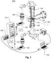
- FIG. 1 shows a quantum computing device 100 according to a possible implementation of the present disclosure that is configured for performing steps of a quantum computing method as disclosed herein (for example methods see FIG. 10 and FIG. 11 below).
- Neutral atoms that serve as qubits are trapped in an optical trap array 110 inside a vacuum chamber 120 that allows for optical access, e.g., a glass vacuum cell.
- the optical trap array 110 may be an array of optical dipole traps, e.g., generated using a digital micro mirror device (DMD), a spatial light modulator (SLM), or an integrated photonics unit for local addressing 130, and imaged to a plane inside the vacuum chamber 120 by a high-resolution imaging system 140.
- DMD digital micro mirror device
- SLM spatial light modulator
- the optical trap array 110 may also be formed by individual planes of an optical lattice.
- neutral atoms are first laser cooled, e.g., via a magneto-optical-trap (MOT) operated inside the vacuum chamber 120 and loaded from an atom source such as a Zeeman slower (not shown).
- Laser cooled neutral atoms can then be loaded into the optical trap array 110 and cooled further to or close to the motional ground state of the optical trap array 110 to initialize an array of essentially identical qubits. Further details of the qubit array initialization sequence are discussed with reference to FIG. 3 below.
- two internal states of the neutral atoms serve as qubit ground state
- a spin-singlet electronic ground state e.g., 1 S 0
- a metastable excited spin triplet state e.g., 3 P 0
- the qubits trapped in the optical trap array 110 thereby form an atomic quantum register that can be used for quantum computation and quantum simulation.
- the quantum computing device 100 uses several laser systems to control the internal states of the neutral atoms.
- local single-qubit gates with arbitrary SU(2) rotations can be realized using a (global) qubit state transition laser 150 in combination with a qubit addressing laser 160 that allows for selective and local control of individual qubits in the optical trap array 110.
- the qubit addressing laser system comprises a laser source comprised in the laser system rack 170, and an integrated photonics qubit addressing unit 162 coupled to the laser source via an optical fiber 164.
- the qubit addressing laser system further comprises a high-resolution imaging system 166, as well as laser frequency and pulse area (e.g., pulse shape and amplitude) controllers that may be included in the laser system rack 170 and / or in the integrated photonics qubit addressing unit 162 (for further details and options see FIG. 5 ).
- the quantum computing device 100 further comprises a modular control signal unit 180 generating various analog, digital and RF control and drive signals needed for precise and fully timed control of laser systems, a magnetic field system (not shown), a qubit read-out system (e.g., comprising a CMOS camera 195 for fluorescence imaging using the high-resolution imaging system 166 of the qubit addressing laser system), etc.
- a modular control signal unit 180 generating various analog, digital and RF control and drive signals needed for precise and fully timed control of laser systems, a magnetic field system (not shown), a qubit read-out system (e.g., comprising a CMOS camera 195 for fluorescence imaging using the high-resolution imaging system 166 of the qubit addressing laser system), etc.
- the qubit addressing laser system (for details see FIG. 5 , FIG. 6 and FIG. 7 ) is configured for locally and selectively illuminating individual qubits with a qubit addressing laser pulse at a first qubit addressing laser frequency to cause a differential Stark shift for the qubit ground state
- the qubit addressing laser 150 can be controlled to locally and selectively illuminate one or more pairs of qubits prepared in the qubit ground state
- both, the qubit state transition laser system and the Rydberg laser system do not require local control for realizing arbitrary single and two qubit quantum gates. Instead, both laser systems can be designed such that they only need to globally illuminate the optical trap array 110, while only the qubit addressing laser system needs to include opto-electronic control equipment for selectively and locally illuminating individual qubits, and pairs of individual qubits in the optical trap array. As discussed above, the qubit addressing laser system may also be used for laser cooling (e.g., sideband cooling) of the neutral atoms during qubit array initialization and / or during qubit state readout to further reduce hardware complexity.
- laser cooling e.g., sideband cooling
- the modular control signal unit 180 and, optionally, the laser system rack 170 may obtain single-qubit and two-qubit gate operation instructions of a quantum computing protocol (e.g., from a digital computer 195 or via an interface to a cloud-computing system) and, in response, control operation of the qubit addressing laser 150 to locally and selectively illuminate individual qubits and pairs of individual qubits to perform single and two-qubit gate operations according to the obtained qubit gate operation instructions.
- the modular control signal unit 180 may also obtain and process instructions for qubit array initialization and / or qubit read-out as disclosed herein.
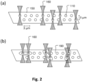
- FIG. 2 shows zoom-in on a portion of the optical trap array 110 having a uniform spacing of 3 ⁇ m to illustrate conceptually how local single-qubit gates (see panel a) and local two-qubit gates (see panel b) can be realized with a quantum computing device as shown in FIG. 1 .
- the optical trap array 110 is globally illuminated by the qubit transition laser 150 to transfer illuminated qubits prepared in the qubit ground state
- the qubit addressing laser 160 can be controlled to selectively and locally illuminate individual qubits to generate arbitrary SU(2) rotations, e.g., via a laser pulse sequence as illustrated in Fig. 5 below and described above.
- the optical trap array 110 is globally illuminated by the Rydberg laser 190 to couple the third internal state
- the qubit addressing laser 160 can be controlled to selectively and locally illuminate individual qubits to perform Rydberg-blockade-based two-qubit gates as illustrated in FIG. 7 below.
- the present disclosure thus also relates to a neutral atom quantum computing device 100, that may comprise a trapping laser system creating an array of optical traps 110 for neutral atoms that serve as qubits for the quantum computing device 100, wherein a first internal state of the neutral atoms serves as qubit ground state
- the disclosed quantum computing device may also comprise a qubit state transition laser system configured for globally illuminating the array of optical traps 110 to transfer qubits prepared in the qubit ground state
- the device 100 may further a qubit addressing laser system (for an example see Fig.
- the quantum computing device 100 may further comprise a Rydberg laser system configured for globally illuminating the array of optical traps 110 to couple the third internal state c> to the Rydberg state
- a Rydberg laser system configured for globally illuminating the array of optical traps 110 to couple the third internal state c> to the Rydberg state
- a qubit readout system using fluorescence emitted by the trapped atoms during a qubit readout sequence.
- such a neutral atom quantum computing device 100 may comprise means /may be configured to carry out the quantum computations methods disclosed herein, such as the methods discussed above and below with reference to FIG. 10 and FIG. 11 .
- the neutral atom quantum computing device 100 may comprise a qubit addressing laser system as disclosed herein, e.g. as discussed above or with reference to FIG. 5 below.
- the neutral atom quantum computing device 100 may comprise a magnetic field system to generate a magnetic field at the location of the optical trap array 110 that defines an angular momentum quantization axis for the neutral atoms and causes a perturbative admixture of a dipole-allowed state to the qubit excited state.
- FIG. 3 illustrates a typical operation sequence of a neutral atom quantum device according to a possible implementation of the present disclosure such as the quantum computing device 100 shown in FIG. 1 .
- the exemplary operation sequence starts with laser cooling of neutral atoms.
- neutral 88 Sr atoms are first laser cooled using a blue MOT e.g. operated using the broad 1 S o to 1 P 1 transition (see Fig. 4 below) followed by a red MOT operated on the narrower 1 S o to 3 P 1 transition that is also used by the qubit addressing laser.
- the substantially narrower linewidth of the 1 S o to 3 P 1 transition allows to further decrease the temperature of the 88 Sr atoms due to the lower Doppler cooling limit that is proportional to the natural linewidth of the laser cooling transition.
- Laser cooled neutral atoms are then loaded into the optical trap array to form a qubit array and are then imaged, e.g., via fluorescence imaging comprising sideband cooling as described below, to detect potential defects in the qubit array that can then be removed during a subsequent atom sorting procedure resulting in a qubit array with unity filling.
- sideband cooling e.g., using the qubit addressing laser system cools the neutral atoms to or close to the motional ground state of the optical trap array to prepare an array of essentially identical qubits that may then be used to execute quantum computation protocols typically comprising execution of multiple local single and local two-qubits gates.
- the internal state of the qubits can be read-out, e.g., via loss-less and state-sensitive fluorescence imaging as discussed with reference to Fig. 8 below.
- Performing sideband cooling, e.g., using a global illumination path of the qubit addressing laser system (cf. FIG. 5 below) during and / or after the qubit read-out sequence allows to reuse the qubit array for performing a subsequent quantum computation protocol without the need to perform laser cooling and optical trap loading to initialize the qubit array.
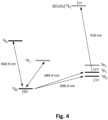
- FIG. 4 shows an atomic level scheme of the bosonic Strontium isotope 88 Sr that can be used as physical qubit in some implementations of the present disclosure.
- 0> can be implemented by the spin singlet state 1 S o of the electronic ground state and the qubit excited state
- the dipole transition matrix element for these two states vanishes due to angular momentum selection rules and
- a qubit addressing laser system can operate with a design wavelength of 698.4 nm corresponding to the 1 S o to 3 P 1 transition, with a natural linewidth of approximately 2 ⁇ ⁇ 7 kHz.
- the 3 P 1 state of 88 Sr is an example of an internal state (designated as third internal state
- c> may serve as an initial state for an optical transition to a highly excited Rydberg state
- the qubit addressing laser system can selectively and locally transfer one or more individual qubits to the third internal state
- c> is also designated as a shelving state herein.
- qubits can be shelved in
- the qubit addressing laser can also be used for sideband cooling of the neutral atoms, e.g., during qubit array initialization and/or qubit state readout.
- the qubit addressing laser can also be operated farther detuned (e.g., ⁇ 1Ghz) from the 1 S o to 3 P 1 resonance thereby causing a differential AC Stark shift for the
- s> such as 1/ ⁇ 2 (0> +
- c> can also be transferred to the Rydberg state
- operating the qubit addressing laser at two different laser frequencies allows to realize local single and local two qubit gates without requiring a selective position control for the qubit state transition laser system and for the Rydberg laser system.
- the qubit state transition laser system and the Rydberg laser system can thus be operated at a fixed laser frequency and don't require sophisticated optoelectronic hardware for position control and arbitrary pulse area control.
- initial laser cooling of the 88 Sr atoms e.g., for operating a Zeeman slower or a blue MOT can be performed on a broad, dipole-allowed 1 S o to 1 P 1 transition at a design wavelength of ⁇ 460.9 nm.
- the same transition can also be used for fluorescence imaging during qubit state readout (see FIG. 8 below).
- FIG. 5 shows a functional block diagram of a qubit addressing laser system 500 according to a possible implementation of the present disclosure.
- the qubit addressing laser system 500 includes a laser source 510, e.g., an extended-cavity diode laser amplified by a tapered amplifier and frequency stabilized to a high-finesse cavity by the Pound-Drever-Hall technique.
- a laser amplifier may be injection locked to an extended-cavity diode laser that may be frequency stabilized to a frequency comb.
- the output of the laser source 510 may be split into two paths by a beam splitter 520, e.g., a polarizing beam splitter or a similar optical element, wherein the first path can be used for selective and local illumination of individual qubits and the second path can be used for global illumination of the qubit array.
- the laser source 510 may comprise two or more individual lasers employing a relative frequency stabilization mechanism, such as injection locking, optical beat locking, etc. to provide two independent illumination paths at with shifted laser frequency.
- the first output of the beam splitter 520 may go through a controllable laser frequency shifter 520, such as an Acousto-Optic Frequency Shifter (AOFS) that modifies the frequency of the optical beam via the Doppler effect.
- AOFS Acousto-Optic Frequency Shifter
- the acoustic wave travelling through the device's crystal causes the frequency of the laser beam to change in proportion to an RF driving frequency.
- an AOM in double-pass configuration or a fiber-coupled laser frequency shifter can be used to apply a controllable frequency shift as large as 1.5GHz while essentially maintaining laser beam pointing stability.
- an optical pulse width / pulse shape controller 530 such as an AOM driven by a controllable RF signal can be employed.
- pulse width / shape control can also be performed via the frequency shifter 520, e.g., via driving the frequency shifter with pulsed RF signal of controllable pulse width / shape.
- both paths may also comprise an optomechanical switch / shutter (not shown).
- the qubit addressing laser system 500 further comprises a 2D focus position controller 550 followed by a high-resolution imaging system 560 as shown in the example of FIG. 1 .
- the optical elements 520 to 560 allow to selectively address one or more qubits in the optical trap array 595 with at a controllable laser frequency and with a controllable pulse area.
- the frequency shifter 520 can be controlled, e.g., via controlling the frequency of the RF driver (not shown) to shift the laser frequency to be red detuned with respect to the
- 1> needed for arbitrary SU(2) rotations can be controlled using the pulse width / pulse shape controller 530 to adjust the pulse area of the laser pulse causing the differential Stark shift while selective qubit addressing is provided by the 2D focus position controller 550.
- the 2D focus position controller 550 may comprising two orthogonal AODs in series that are driven by multiple RF tones with controllable RF frequency.
- focus position control may also be realized using a DMD, an SLM or integrated photonics addressing unit as shown in FIG. 1 .
- the controllable laser focus pattern generated by the 2D focus position controller 550 may then be imaged, by the high-resolution imaging system 560, to individual qubits in the optical trap array (see FIG. 2 ) that need to be addressd during local single qubit or two qubit gates and / or for selective shelving to the 3 P 1 state.
- the second output of the beam splitter 520 can be used for global illumination of the optical trap array 595, e.g., as discussed above, for sideband cooling during an initialization sequence and / or a qubit read-out sequence.
- the global illumination path may comprise a frequency shifter 570, that may operate at an essentially fixed frequency shift needed for sideband cooling and an optical switching device 580 which may be a pulse width / shape controller as discussed for the local and selective path above or may be realized using simpler hardware.
- a 2D focus position controller and a high-resolution imaging system are not necessary. Instead, global illumination optics such as an optical fiber and a beam collimator may be used to globally illuminate the optical trap array 395.
- the present disclosure also relates to a qubit addressing laser system 500 for a quantum computing device 100 that uses neutral atoms trapped in an array of optical traps 110 as qubits.
- the qubit addressing laser system 500 may comprise a laser source 510 providing laser light with a design wavelength corresponding to a transition between a first internal state and a second internal state of the neutral atoms that serve as qubit states
- the qubit addressing laser system 500 may comprise a laser frequency controller / shifter 530 to set the frequency of laser light provided by the qubit addressing laser system 500 to a first laser frequency and to a second laser frequency, as well as a pulse width or pulse shape controller 540 to generate laser pulses with a controllable pulse width or pulse shape / area, such that, for the first laser frequency, a phase difference for the qubit ground state
- the qubit addressing laser system 500 may also comprise a laser focus position controller 550 that controls focus positions of the laser light provided by the qubit addressing laser system 500 such that at least two neutral atoms trapped in the array of optical traps 110 can selectively and locally be illuminated simultaneously, e.g., via a high-resolution imaging system 560.
- the laser focus position controller 550 may comprises one or more of an acousto-optic deflector, a digital micromirror device, a spatial light modulator, an electro-optic deflector, and an integrated photonics unit for local addressing 162.
- the laser frequency controller 530 may comprises one or more of an acousto-optic modulator, an acousto-optic-frequency shifter, and an optical phase locked loop
- the pulse width or pulse shape controller 540 may comprise one or more of an acousto-optic modulator, an acousto-optic deflector, an electro-optic-modulator, and an electro-optic deflector.
- the laser frequency controller 530 or an additional laser frequency controller such as a fixed frequency shifter 570 may be configured to set the frequency of the laser light provided by the qubit addressing laser system 500 to a third laser frequency.
- the qubit addressing laser system 500 may further comprise a global illumination path to globally illuminate the optical trap array 110 with laser light at the third laser frequency to cool trapped atoms via sideband cooling.
- FIG. 6 conceptually illustrates how local single-qubit gates can be realized according to implementations of the present disclosure.
- panel a) of FIG. 6 one dimensional selective qubit addressing by a qubit addressing laser beam 610 combined with global illumination by a qubit state transition laser beam 620 is illustrated.
- the qubit addressing laser system may include an AOD 630 and a large NA imaging objective 640 focusing the output beam(s) of the AOD 630 to an array of optical traps 650 trapping neutral atoms that serve as physical qubits.
- the focus position(s) of the qubit addressing laser beam 610 can be controlled by changing the frequency of the RF signal driving the AOD 630.
- multiple qubits can be accessed simultaneously via driving the AOD 630 with an RF drive signal comprising two or more different RF frequencies, e.g., via a multi-tone RF signal, wherein each tone corresponds to a different deflection angle of the AOD 630.
- Two-dimensional position control can for example realized by using two orthogonal AODs 630 in series.
- Panel b) of FIG. 6 shows a configuration where all atoms are simultaneously illuminated by a global qubit transition laser beam 620 and a local qubit addressing laser pulse 610 locally illuminating all qubits to be addressed simultaneously, e.g., via driving the AOD 630 with a four-tone RF drive signal.
- Panel c) of FIG. 6 illustrates an exemplary pulse sequence for performing a single qubit gate on all four atoms shown in panel b) previously prepared in the qubit ground state
- the shown single qubit gate operation comprise a first global qubit state transition laser pulse 650 (e.g., a ⁇ /2 - pulse) transferring the four qubits prepared in state
- s> 1/ ⁇ 2 (0> +
- each atom may be illuminated locally and selectively, by a separate qubit addressing laser pulse 660, causing a differential AC Stark shift resulting in a phase difference ⁇ between
- s ⁇ > 1/ ⁇ 2 (0>e i ⁇ +
- the AC Stark shift pulse 660 can be applied sequentially for each individual qubit or they may also be applied simultaneously for all addressd qubits.
- 1> can be adjusted to any value between from 0° to 180°.
- a second global qubits transition laser pulse 670 is applied that transfers all atoms that were not illuminated by the local AC Stark shifting pulse back to
- the single-qubit gate sequence shown in panel b) of FIG. 6 may comprise additional AC Stark shift pulses 680 and 690 that may be needed for quantum computation protocols where the addressing qubits are not initially prepared in the qubit ground state
- FIG. 7 illustrates how local two-qubit gates, that are needed for generating entanglement (e.g., Bell states, W-states, GHZ-sates, etc.) during quantum computation can be realized according to implementations of the present disclosure.
- entanglement e.g., Bell states, W-states, GHZ-sates, etc.
- the qubit addressing laser system may include an AOD 730 and a large NA imaging objective 740 focusing the output beam(s) of the AOD 730 to an array of optical traps 750 trapping neutral atoms as physical qubits.
- the focus position(s) of the qubit addressing laser beam 710 can be controlled by changing the frequency of the RF signal driving the AOD 730.
- multiple qubits can be accessed simultaneously via driving the AOD 730 with a multi-tone RF drive signal.
- two neighboring atoms e.g., atom 2 and atom 3 in panel b
- two neighboring atoms are first transferred to the shelving state
- the optical trap array 750 is globally illuminated by a Rydberg laser pulse 770 that only interacts with atoms prepared in the shelving state
- Rydberg-blockade caused by dipole interactions between atom 2 and atom 3 in the Rydberg state
- e> 1/ ⁇ 2 (
- more general superposition states can also be generated when performing a two-qubit gate based on Rydberg-blockade.
- Rydberg rotation 770 may also done detuned from resonance, e.g., for implementing a Lavine-Pichler gate or a time optimal gate as mentioned above.
- the qubit addressing laser can be used to generate a controlled phase shift for
- a phase shifting pulse 780 can be interspersed with two global Rydberg laser pulses 770 and 790.
- the pulse duration of the phase shifting pulse 780 and the detuning of the Rydberg laser can be controlled to realize a controlled phase gate.
- phase shifting pulse 780 is applied during a single global Rydberg laser pulse 770, to maintain entanglement after the inverse shelving pulse 790.
- selective laser position control for the qubit addressing laser 710 can be realized using different technology, such the integrated photonics addressing units 130, 162 shown in FIG. 1 .
- FIG. 8 illustrates how the qubit addressing laser can also be used for sideband cooling during a qubit readout sequence based on fluorescence imaging on the 1 S o to 1 P 1 transition in 88 Sr using an imaging laser with a design wavelength of 461 nm.
- the optical trap array is illuminated by the imaging laser such that atoms excited to the 1 P 1 state spontaneously decay to the 1 S o state via emitting a fluorescence photon that can be detected by a CMOS camera (see FIG. 1 ). Due to the cycling nature of this transition, multiple fluorescence photons can be collected for each qubit in the 1 S o state to detect which qubits where in the
- the optical trap array can simultaneously be illuminated by the qubit addressing laser at the third laser frequency to perform sideband cooling counteracting the heating caused by the imaging laser and the recoil of spontaneous emission of fluorescence photons.
- the qubits addressing laser can also be used to detect which qubits are in the
- the qubit addressing laser also allows state selective and essentially loss-less qubit readout substantially improving cycle times and reducing hardware complexity as compared to conventional systems.
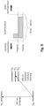
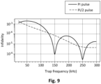
- FIG. 9 illustrates how, according to the present disclosure, the effective (combined) pulse duration of a single ⁇ -pulse or two consecutive ⁇ /2-pulses of the (global) qubit state transition laser can be chosen to minimize gate infidelity caused by motional dephasing.
- illuminating the optical trap array with a single qubit state transition laser pulse or with two consecutive qubit state transition laser pulses having an effective (combined) pulse duration that equals ⁇ / ⁇ 2n+1, nEN, where ⁇ is the Rabi frequency associated with the qubit state transition laser and the
- the present disclosure allows to operate the qubit state transition laser as cleanly as possible facilitating low phase noise, as well as increased frequency and amplitude stability.
- the present invention allows to keep the effective Rabi frequency ⁇ , which in general depends on phase noise, detuning with respect to the
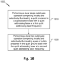
- FIG. 10 shows a process diagram of a method for quantum computing 1000.
- a local single-qubit gate operation may be performed comprising locally and selectively illuminating a qubit prepared in a superposition state with a qubit addressing laser at a first qubit addressing laser frequency
- a local two-qubit gate operation comprising locally and selectively illuminating a pair of qubits prepared in the qubit ground state with the qubit addressing laser at a second qubit addressing laser frequency.
- the method of FIG. 10 may further comprise performing, using the qubit addressing laser, sideband cooling during a qubit initialization sequence and / or during a qubit readout sequence, comprising globally illuminating the array of optical traps with the qubit addressing laser at a third qubit addressing laser frequency, or locally and selectively illuminating a qubit with the qubit addressing laser at the third qubit addressing laser frequency.
- performing the local single qubit gate operation 1010 may further comprise globally illuminating the array of optical traps with a first qubit state transition laser pulse to transfer qubits prepared in the qubit ground state
- performing the local two-qubit gate operation 1020 may further comprise globally illuminating the array of optical traps with a Rydberg laser pulse to transfer the one or more pairs of qubits to the Rydberg state
- the method of FIG. 10 may further comprise locally and selectively illuminating the one or more pairs of qubits with the qubit addressing laser at a fourth qubit addressing laser frequency or at the first qubit addressing laser frequency to cause a differential AC Stark shift for the third internal state
- a dipole-allowed state e.g.,
- performing the qubit initialization sequence may comprise loading the plurality of neutral atoms into the optical trap array, performing the sideband cooling to transfer the neutral atoms into motional ground states of the optical trap array.
- performing the qubit readout sequence may further comprise performing the sideband cooling while globally illuminating the optical trap array with an imaging laser, and imaging the qubits using fluorescence induced by the imaging laser.
- performing the qubit readout sequence may further comprise selectively and locally illuminating a qubit with a qubit addressing laser pulse at the second qubit addressing laser frequency to transfer the qubit to the third internal state
- the optical trap array may comprises a trap frequency ⁇ that may essentially be the same for all qubits
- neutral atoms may comprise bosonic 88 Sr atoms
- the qubit addressing laser may have a design wavelength of 689.4 nm
- the Rydberg laser may have a design wavelength of 318.5 nm
- the qubit state transition laser may have a design wavelength of 698.4 nm.
- the method disclosed herein may also comprise shifting the laser frequency of the qubit addressing laser to the first qubit addressing laser frequency, shifting the laser frequency of the qubit addressing laser to the second qubit addressing laser frequency, shifting the laser frequency of the qubit addressing laser to the third qubit addressing laser frequency.
- the method disclosed herein may comprise performing multiple single-qubit and two-qubit gate operations, and periodically driving the qubit addressing laser to generate a first laser pulse train with a constant inter-pulse duration for performing multiple single-qubit and two-qubit gate operations. Further, the method disclosed herein may further comprise periodically driving the qubit addressing laser to generate a second laser pulse train with a constant inter-pulse duration, and controlling the spacing between the first laser pulse train and the second laser pulse train as well as synchronizing the periodic driving of the qubit addressing laser with a characteristic frequency of an external noise source affecting qubit gate fidelity.
- single-qubit and two-qubit gate operation instructions of a quantum computing protocol may be obtained, and the operation of the qubit addressing laser to locally and selectively illuminate a plurality of qubits and a plurality of pairs of qubits to perform single and two-qubit gate operations may be controlled according to the obtained qubit gate operation instructions.
- FIG. 11 includes steps 1010 and 1020 of FIG. 10 designated as steps 1120 and 1130 as well as a step 1110, where as discussed above, a qubit initialization sequence may be performed using the qubit addressing laser at a third qubit addressing laser frequency, and step 1140, where, as also discussed above, a qubit readout sequence using the qubit addressing laser at the third qubit addressing laser frequency may be performed by a quantum computing device such as the possible implementation of FIG. 1 .
- the term component is intended to be broadly construed as hardware, firmware, or a combination of hardware and software.
- a processor is implemented in hardware, firmware, or a combination of hardware and software.
- "at least one of: a, b, or c” is intended to cover a, b, c, a-b, a-c, b-c, and a-b-c, as well as any combination with multiples of the same element (e.g., a-a, a-a-a, a-a-b, a-a-c, a-b-b, a-c-c, b-b, b-b-b, b-b-c, c-c, and c-c-c or any other ordering of a, b, and c).
- the phrase "based on” shall not be construed as a reference to a closed set of information, one or more conditions, one or more factors, or the like.
- the phrase “based on A” (where “A” may be information, a condition, a factor, or the like) shall be construed as “based at least on A” unless specifically recited differently.
- the term "or” is an inclusive “or” unless limiting language is used relative to the alternatives listed.
- reference to "X being based on A or B” shall be construed as including within its scope X being based on A, X being based on B, and X being based on A and B.
- reference to "X being based on A or B” refers to "at least one of A or B” or “one or more of A or B” due to "or” being inclusive.
- reference to "X being based on A, B, or C" shall be construed as including within its scope X being based on A, X being based on B, X being based on C, X being based on A and B, X being based on A and C, X being based on B and C, and X being based on A, B, and C.
- reference to "X being based on A, B, or C” refers to "at least one of A, B, or C" or “one or more of A, B, or C" due to "or” being inclusive.
- X being based on only one of A or B shall be construed as including within its scope X being based on A as well as X being based on B, but not X being based on A and B.
- process diagrams such as FIG. 10 and FIG. 11 do not necessarily indicate a particular order or sequence of steps.
- steps 1010 and 1120 of FIG. 10 , or steps 1120 and 1130 in FIG. 11 may also be performed in a different order or, if hardware capabilities allow it, simultaneously, without deviating from the scope of the present disclosure.
Landscapes
- Engineering & Computer Science (AREA)
- Physics & Mathematics (AREA)
- Theoretical Computer Science (AREA)
- General Physics & Mathematics (AREA)
- Software Systems (AREA)
- Data Mining & Analysis (AREA)
- General Engineering & Computer Science (AREA)
- Condensed Matter Physics & Semiconductors (AREA)
- Mathematical Analysis (AREA)
- Mathematical Optimization (AREA)
- Pure & Applied Mathematics (AREA)
- Computing Systems (AREA)
- Evolutionary Computation (AREA)
- Mathematical Physics (AREA)
- Computational Mathematics (AREA)
- Artificial Intelligence (AREA)
- Optical Modulation, Optical Deflection, Nonlinear Optics, Optical Demodulation, Optical Logic Elements (AREA)
- Electromagnetism (AREA)
- Plasma & Fusion (AREA)
- Optics & Photonics (AREA)
Priority Applications (8)
| Application Number | Priority Date | Filing Date | Title |
|---|---|---|---|
| EP23181879.0A EP4485291B1 (de) | 2023-06-27 | 2023-06-27 | Hardwareeffizientes neutralatomquantenberechnungsverfahren und vorrichtung |
| AU2024311033A AU2024311033A1 (en) | 2023-06-27 | 2024-06-18 | Hardware-efficient neutral atom quantum computing method and device |
| KR1020267002216A KR20260026568A (ko) | 2023-06-27 | 2024-06-18 | 하드웨어 효율적인 중성 원자 양자 컴퓨팅 방법 및 디바이스 |
| CN202480043262.8A CN121620764A (zh) | 2023-06-27 | 2024-06-18 | 硬件高效的中性原子量子计算方法与装置 |
| PCT/EP2024/066941 WO2025002913A1 (en) | 2023-06-27 | 2024-06-18 | Hardware-efficient neutral atom quantum computing method and device |
| US18/755,715 US12614098B2 (en) | 2023-06-27 | 2024-06-27 | Hardware-efficient neutral atom quantum computing method and device |
| MX2025015307A MX2025015307A (es) | 2023-06-27 | 2025-12-16 | Método y dispositivo de computación cuántica eficiente en hardware con átomos neutros |
| IL325513A IL325513A (en) | 2023-06-27 | 2025-12-22 | A hardware-efficient neutral atomic quantum computing method and device |
Applications Claiming Priority (1)
| Application Number | Priority Date | Filing Date | Title |
|---|---|---|---|
| EP23181879.0A EP4485291B1 (de) | 2023-06-27 | 2023-06-27 | Hardwareeffizientes neutralatomquantenberechnungsverfahren und vorrichtung |
Publications (2)
| Publication Number | Publication Date |
|---|---|
| EP4485291A1 true EP4485291A1 (de) | 2025-01-01 |
| EP4485291B1 EP4485291B1 (de) | 2026-04-22 |
Family
ID=87003248
Family Applications (1)
| Application Number | Title | Priority Date | Filing Date |
|---|---|---|---|
| EP23181879.0A Active EP4485291B1 (de) | 2023-06-27 | 2023-06-27 | Hardwareeffizientes neutralatomquantenberechnungsverfahren und vorrichtung |
Country Status (8)
| Country | Link |
|---|---|
| US (1) | US12614098B2 (de) |
| EP (1) | EP4485291B1 (de) |
| KR (1) | KR20260026568A (de) |
| CN (1) | CN121620764A (de) |
| AU (1) | AU2024311033A1 (de) |
| IL (1) | IL325513A (de) |
| MX (1) | MX2025015307A (de) |
| WO (1) | WO2025002913A1 (de) |
Families Citing this family (1)
| Publication number | Priority date | Publication date | Assignee | Title |
|---|---|---|---|---|
| CN120579650B (zh) * | 2025-08-05 | 2025-10-28 | 中电信量子信息科技集团有限公司 | 离子量子比特寻址系统和离子量子比特寻址方法 |
Family Cites Families (1)
| Publication number | Priority date | Publication date | Assignee | Title |
|---|---|---|---|---|
| EP4548269A2 (de) * | 2022-07-01 | 2025-05-07 | Atom Computing Inc. | Verfahren und systeme zur unterdrückung inkohärenter streuung |
-
2023
- 2023-06-27 EP EP23181879.0A patent/EP4485291B1/de active Active
-
2024
- 2024-06-18 WO PCT/EP2024/066941 patent/WO2025002913A1/en not_active Ceased
- 2024-06-18 AU AU2024311033A patent/AU2024311033A1/en active Pending
- 2024-06-18 CN CN202480043262.8A patent/CN121620764A/zh active Pending
- 2024-06-18 KR KR1020267002216A patent/KR20260026568A/ko active Pending
- 2024-06-27 US US18/755,715 patent/US12614098B2/en active Active
-
2025
- 2025-12-16 MX MX2025015307A patent/MX2025015307A/es unknown
- 2025-12-22 IL IL325513A patent/IL325513A/en unknown
Non-Patent Citations (7)
| Title |
|---|
| ALEXANDER BAUMG�RTNER: "A new apparatus for trapping and manipulating single Strontium atoms", UNIVERSITY OF HEIDELBERG, 1 January 2017 (2017-01-01), XP055705136, Retrieved from the Internet <URL:https://www.kip.uni-heidelberg.de/Veroeffentlichungen/download/6081/pdf-6081.pdf> [retrieved on 20200615] * |
| H. LEVINE ET AL.: "Parallel Implementation of High-Fidelity Multiqubit Gates with Neutral Atoms", PHYS. REV. LETT. 123 |
| JOANNA W LIS ET AL: "Mid-circuit operations using the omg-architecture in neutral atom arrays", ARXIV.ORG, CORNELL UNIVERSITY LIBRARY, 201 OLIN LIBRARY CORNELL UNIVERSITY ITHACA, NY 14853, 21 June 2023 (2023-06-21), XP091543938 * |
| LEVINE HARRY ET AL: "Parallel implementation of high-fidelity multi-qubit gates with neutral atoms", 20 August 2019 (2019-08-20), arXiv.org, pages 1 - 16, XP093108073, Retrieved from the Internet <URL:https://arxiv.org/pdf/1908.06101.pdf> [retrieved on 20231201] * |
| MORGADO M ET AL: "Quantum simulation and computing with Rydberg qubits", ARXIV.ORG, CORNELL UNIVERSITY LIBRARY, 201 OLIN LIBRARY CORNELL UNIVERSITY ITHACA, NY 14853, 5 November 2020 (2020-11-05), XP081797032 * |
| PASCAL SCHOLL ET AL: "Erasure conversion in a high-fidelity Rydberg quantum simulator", ARXIV.ORG, CORNELL UNIVERSITY LIBRARY, 201 OLIN LIBRARY CORNELL UNIVERSITY ITHACA, NY 14853, 5 May 2023 (2023-05-05), XP091502336 * |
| UNKNOWN UNKNOWN: "How does |00> evolve through an Hadamard and a CNOT gate?", 10 May 2021 (2021-05-10), pages 1 - 2, XP093138798, Retrieved from the Internet <URL:https://quantumcomputing.stackexchange.com/questions/17425/how-does-00-rangle-evolve-through-an-hadamard-and-a-cnot-gate> [retrieved on 20240307] * |
Also Published As
| Publication number | Publication date |
|---|---|
| AU2024311033A1 (en) | 2026-01-29 |
| IL325513A (en) | 2026-02-01 |
| EP4485291B1 (de) | 2026-04-22 |
| MX2025015307A (es) | 2026-04-01 |
| WO2025002913A1 (en) | 2025-01-02 |
| US20250005420A1 (en) | 2025-01-02 |
| KR20260026568A (ko) | 2026-02-26 |
| US12614098B2 (en) | 2026-04-28 |
| CN121620764A (zh) | 2026-03-06 |
Similar Documents
| Publication | Publication Date | Title |
|---|---|---|
| Lis et al. | Midcircuit operations using the omg architecture in neutral atom arrays | |
| US7779228B2 (en) | Quantum information processing device and method | |
| US12367414B2 (en) | Methods and apparatuses for barium states preparations for quantum operations | |
| US12614098B2 (en) | Hardware-efficient neutral atom quantum computing method and device | |
| US12288133B2 (en) | Methods and apparatuses for electromagnetically-induced transparency cooling in an isotope with a nuclear spin of 3/2 or greater | |
| US12518193B2 (en) | Methods and apparatuses for stray field compensation by laser beam referencing | |
| Marinelli | Quantum information processing with mixed-species ion crystals | |
| Yu et al. | In situ midcircuit qubit measurement and reset in a single-species trapped-ion quantum computing system | |
| Riebe | Preparation of entangled states and quantum teleportation with atomic qubits | |
| NL2033936B1 (en) | Quantum logic gate for a trapped ion quantum computer | |
| US12164072B2 (en) | Methods and apparatuses for micromotion compensation with displaced beam | |
| Hartmann et al. | Attosecond coherent control at FELs | |
| RU2814970C1 (ru) | Квантовая вычислительная система на основе нейтральных атомов | |
| US20250005425A1 (en) | Cloud-accessible quantum simulator based on programmable atom arrays | |
| US20260044767A1 (en) | Quantum computing with spectator qubits | |
| Erickson | Mixed-Species Quantum Logic with Trapped Ions for Gate Teleportation, Metrology, and High-Fidelity Indirect Readout | |
| Thomm | Towards quantum simulation and computing with trapped Rydberg ions | |
| EP4602529A2 (de) | Verfahren und vorrichtungen zur doppler-kühlung | |
| Tsui | Subwavelength Spatial Control and Measurement of Cold Atoms via Optical Nonlinearity and a New Experimental Platform for Two-Species Atom Tweezer Arrays | |
| WO2026027788A1 (en) | Methods and apparatus for generating quantum entanglement | |
| Heinrich et al. | Ultrafast coherent excitation of a Ca $^+ $ ion | |
| WO2023027795A2 (en) | Dual-space, single-species architecture for trapped-ion quantum information processing | |
| Walsh | Microwave and optical control of sub-diffraction spin qubits in diamond at cryogenic temperatures |
Legal Events
| Date | Code | Title | Description |
|---|---|---|---|
| PUAI | Public reference made under article 153(3) epc to a published international application that has entered the european phase |
Free format text: ORIGINAL CODE: 0009012 |
|
| STAA | Information on the status of an ep patent application or granted ep patent |
Free format text: STATUS: THE APPLICATION HAS BEEN PUBLISHED |
|
| AK | Designated contracting states |
Kind code of ref document: A1 Designated state(s): AL AT BE BG CH CY CZ DE DK EE ES FI FR GB GR HR HU IE IS IT LI LT LU LV MC ME MK MT NL NO PL PT RO RS SE SI SK SM TR |
|
| STAA | Information on the status of an ep patent application or granted ep patent |
Free format text: STATUS: REQUEST FOR EXAMINATION WAS MADE |
|
| 17P | Request for examination filed |
Effective date: 20250701 |
|
| GRAP | Despatch of communication of intention to grant a patent |
Free format text: ORIGINAL CODE: EPIDOSNIGR1 |
|
| STAA | Information on the status of an ep patent application or granted ep patent |
Free format text: STATUS: GRANT OF PATENT IS INTENDED |
|
| INTG | Intention to grant announced |
Effective date: 20251117 |
|
| GRAS | Grant fee paid |
Free format text: ORIGINAL CODE: EPIDOSNIGR3 |
|
| GRAA | (expected) grant |
Free format text: ORIGINAL CODE: 0009210 |
|
| STAA | Information on the status of an ep patent application or granted ep patent |
Free format text: STATUS: THE PATENT HAS BEEN GRANTED |
|
| RIN1 | Information on inventor provided before grant (corrected) |
Inventor name: BLATT, SEBASTIAN Inventor name: BLOCH, IMMANUEL Inventor name: ALBERTI, ANDREA Inventor name: ZEIHER, JOHANNES Inventor name: FESTA, LORENZO Inventor name: MELCHNER VON DYDIOWA, MAX ROBERT Inventor name: EBERHARD, ROBIN Inventor name: ZHANG, ZHAO Inventor name: MOURS, KEVIN Inventor name: TSEVAS, DIMITRIOS |
|
| AK | Designated contracting states |
Kind code of ref document: B1 Designated state(s): AL AT BE BG CH CY CZ DE DK EE ES FI FR GB GR HR HU IE IS IT LI LT LU LV MC ME MK MT NL NO PL PT RO RS SE SI SK SM TR |
|
| REG | Reference to a national code |
Ref country code: CH Ref legal event code: F10 Free format text: ST27 STATUS EVENT CODE: U-0-0-F10-F00 (AS PROVIDED BY THE NATIONAL OFFICE) Effective date: 20260422 Ref country code: GB Ref legal event code: FG4D |