EP4485208A1 - Vorrichtung und verfahren zur sanften verschlechterung redundanter verarbeitung - Google Patents
Vorrichtung und verfahren zur sanften verschlechterung redundanter verarbeitung Download PDFInfo
- Publication number
- EP4485208A1 EP4485208A1 EP23212880.1A EP23212880A EP4485208A1 EP 4485208 A1 EP4485208 A1 EP 4485208A1 EP 23212880 A EP23212880 A EP 23212880A EP 4485208 A1 EP4485208 A1 EP 4485208A1
- Authority
- EP
- European Patent Office
- Prior art keywords
- processing
- processing elements
- processing element
- error
- circuitry
- Prior art date
- Legal status (The legal status is an assumption and is not a legal conclusion. Google has not performed a legal analysis and makes no representation as to the accuracy of the status listed.)
- Pending
Links
Images


Classifications
-
- G—PHYSICS
- G06—COMPUTING OR CALCULATING; COUNTING
- G06F—ELECTRIC DIGITAL DATA PROCESSING
- G06F11/00—Error detection; Error correction; Monitoring
- G06F11/07—Responding to the occurrence of a fault, e.g. fault tolerance
- G06F11/16—Error detection or correction of the data by redundancy in hardware
- G06F11/18—Error detection or correction of the data by redundancy in hardware using passive fault-masking of the redundant circuits
- G06F11/183—Error detection or correction of the data by redundancy in hardware using passive fault-masking of the redundant circuits by voting, the voting not being performed by the redundant components
- G06F11/184—Error detection or correction of the data by redundancy in hardware using passive fault-masking of the redundant circuits by voting, the voting not being performed by the redundant components where the redundant components implement processing functionality
-
- G—PHYSICS
- G06—COMPUTING OR CALCULATING; COUNTING
- G06F—ELECTRIC DIGITAL DATA PROCESSING
- G06F11/00—Error detection; Error correction; Monitoring
- G06F11/07—Responding to the occurrence of a fault, e.g. fault tolerance
- G06F11/16—Error detection or correction of the data by redundancy in hardware
- G06F11/18—Error detection or correction of the data by redundancy in hardware using passive fault-masking of the redundant circuits
- G06F11/181—Eliminating the failing redundant component
-
- G—PHYSICS
- G06—COMPUTING OR CALCULATING; COUNTING
- G06F—ELECTRIC DIGITAL DATA PROCESSING
- G06F11/00—Error detection; Error correction; Monitoring
- G06F11/07—Responding to the occurrence of a fault, e.g. fault tolerance
- G06F11/16—Error detection or correction of the data by redundancy in hardware
- G06F11/20—Error detection or correction of the data by redundancy in hardware using active fault-masking, e.g. by switching out faulty elements or by switching in spare elements
- G06F11/202—Error detection or correction of the data by redundancy in hardware using active fault-masking, e.g. by switching out faulty elements or by switching in spare elements where processing functionality is redundant
-
- G—PHYSICS
- G06—COMPUTING OR CALCULATING; COUNTING
- G06F—ELECTRIC DIGITAL DATA PROCESSING
- G06F11/00—Error detection; Error correction; Monitoring
- G06F11/07—Responding to the occurrence of a fault, e.g. fault tolerance
- G06F11/16—Error detection or correction of the data by redundancy in hardware
- G06F11/1629—Error detection by comparing the output of redundant processing systems
- G06F11/1641—Error detection by comparing the output of redundant processing systems where the comparison is not performed by the redundant processing components
-
- G—PHYSICS
- G06—COMPUTING OR CALCULATING; COUNTING
- G06F—ELECTRIC DIGITAL DATA PROCESSING
- G06F11/00—Error detection; Error correction; Monitoring
- G06F11/07—Responding to the occurrence of a fault, e.g. fault tolerance
- G06F11/16—Error detection or correction of the data by redundancy in hardware
- G06F11/1629—Error detection by comparing the output of redundant processing systems
- G06F11/165—Error detection by comparing the output of redundant processing systems with continued operation after detection of the error
-
- G—PHYSICS
- G06—COMPUTING OR CALCULATING; COUNTING
- G06F—ELECTRIC DIGITAL DATA PROCESSING
- G06F13/00—Interconnection of, or transfer of information or other signals between, memories, input/output devices or central processing units
- G06F13/10—Program control for peripheral devices
- G06F13/12—Program control for peripheral devices using hardware independent of the central processor, e.g. channel or peripheral processor
- G06F13/124—Program control for peripheral devices using hardware independent of the central processor, e.g. channel or peripheral processor where hardware is a sequential transfer control unit, e.g. microprocessor, peripheral processor or state-machine
-
- G—PHYSICS
- G06—COMPUTING OR CALCULATING; COUNTING
- G06F—ELECTRIC DIGITAL DATA PROCESSING
- G06F13/00—Interconnection of, or transfer of information or other signals between, memories, input/output devices or central processing units
- G06F13/14—Handling requests for interconnection or transfer
- G06F13/16—Handling requests for interconnection or transfer for access to memory bus
- G06F13/1668—Details of memory controller
- G06F13/1673—Details of memory controller using buffers
-
- G—PHYSICS
- G06—COMPUTING OR CALCULATING; COUNTING
- G06F—ELECTRIC DIGITAL DATA PROCESSING
- G06F13/00—Interconnection of, or transfer of information or other signals between, memories, input/output devices or central processing units
- G06F13/38—Information transfer, e.g. on bus
- G06F13/40—Bus structure
- G06F13/4004—Coupling between buses
- G06F13/4027—Coupling between buses using bus bridges
-
- G—PHYSICS
- G06—COMPUTING OR CALCULATING; COUNTING
- G06F—ELECTRIC DIGITAL DATA PROCESSING
- G06F9/00—Arrangements for program control, e.g. control units
- G06F9/06—Arrangements for program control, e.g. control units using stored programs, i.e. using an internal store of processing equipment to receive or retain programs
- G06F9/30—Arrangements for executing machine instructions, e.g. instruction decode
- G06F9/30098—Register arrangements
- G06F9/3012—Organisation of register space, e.g. banked or distributed register file
- G06F9/30134—Register stacks; shift registers
-
- G—PHYSICS
- G06—COMPUTING OR CALCULATING; COUNTING
- G06F—ELECTRIC DIGITAL DATA PROCESSING
- G06F11/00—Error detection; Error correction; Monitoring
- G06F11/07—Responding to the occurrence of a fault, e.g. fault tolerance
- G06F11/16—Error detection or correction of the data by redundancy in hardware
- G06F11/18—Error detection or correction of the data by redundancy in hardware using passive fault-masking of the redundant circuits
- G06F11/186—Passive fault masking when reading multiple copies of the same data
Definitions
- This invention relates generally to the field of computer processors. More particularly, the invention relates to an apparatus and method for graceful degradation of redundant processing, such as processing by redundant processing elements.
- processor lockstep and/or multiprocessor voting algorithms are employed to detect program flow execution issues. However, once an error is detected, there is no mechanism to allow a system to continue to function with reduced error detection capabilities.
- one or more instructions are fetched from instruction memory
- the one or more fetched instructions may be decoded, addresses (e.g., load store unit (LSU) addresses) using forwarded register ports may be generated, and branch forwarding (e.g., immediate offset or an link register (LR)) may be performed.
- LSU load store unit
- LR link register
- the decode stage 306 and the register read/memory read stage 314 may be combined into one pipeline stage.
- the decoded instructions may be executed, LSU address/data pipelining to an Advanced Microcontroller Bus (AHB) interface may be performed, multiply and add operations may be performed, arithmetic operations with branch results may be performed, etc.
- APB Advanced Microcontroller Bus
- the exemplary register renaming, out-of-order issue/execution core architecture may implement the pipeline 300 as follows: 1) the instruction fetch 338 performs the fetch and length decoding stages 302 and 304; 2) the decode unit circuitry 340 performs the decode stage 306; 3) the rename/allocator unit circuitry 352 performs the allocation stage 308 and renaming stage 310; 4) the scheduler unit(s) circuitry 356 performs the schedule stage 312; 5) the physical register file(s) unit(s) circuitry 358 and the memory unit circuitry 370 perform the register read/memory read stage 314; the execution cluster 360 perform the execute stage 316; 6) the memory unit circuitry 370 and the physical register file(s) unit(s) circuitry 358 perform the write back/memory write stage 318; 7) various units (unit circuitry) may be involved in the exception handling stage 322; and 8) the retirement unit circuitry 354 and the physical register file(s) unit(s) circuitry 3
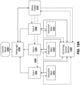
- FIG. 3(B) shows processor core 390 including front-end unit circuitry 330 coupled to an execution engine unit circuitry 350, and both are coupled to a memory unit circuitry 370.
- the core 390 may be a reduced instruction set computing (RISC) core, a complex instruction set computing (CISC) core, a very long instruction word (VLIW) core, or a hybrid or alternative core type.
- the core 390 may be a special-purpose core, such as, for example, a network or communication core, compression engine, coprocessor core, general purpose computing graphics processing unit (GPGPU) core, graphics core, or the like.
- GPGPU general purpose computing graphics processing unit
- the decode unit circuitry 340 may further include an address generation unit circuitry (AGU, not shown).
- AGU address generation unit circuitry
- the AGU generates an LSU address using forwarded register ports, and may further perform branch forwarding (e.g., immediate offset branch forwarding, LR register branch forwarding, etc.).
- the decode unit circuitry 340 may be implemented using various different mechanisms. Examples of suitable mechanisms include, but are not limited to, look-up tables, hardware implementations, programmable logic arrays (PLAs), microcode read only memories (ROMs), etc.
- the core 390 includes a microcode ROM (not shown) or other medium that stores microcode for certain macroinstructions (e.g., in decode unit circuitry 340 or otherwise within the front end unit circuitry 330).
- the decode unit circuitry 340 includes a micro-operation (micro-op) or operation cache (not shown) to hold/cache decoded operations, micro-tags, or micro-operations generated during the decode or other stages of the processor pipeline 300.
- the decode unit circuitry 340 may be coupled to rename/allocator unit circuitry 352 in the execution engine unit circuitry 350.
- the execution engine circuitry 350 includes the rename/allocator unit circuitry 352 coupled to a retirement unit circuitry 354 and a set of one or more scheduler(s) circuitry 356.
- the scheduler(s) circuitry 356 represents any number of different schedulers, including reservations stations, central instruction window, etc.
- the scheduler(s) circuitry 356 can include arithmetic logic unit (ALU) scheduler/scheduling circuitry, ALU queues, arithmetic generation unit (AGU) scheduler/scheduling circuitry, AGU queues, etc.
- ALU arithmetic logic unit
- AGU arithmetic generation unit
- the scheduler(s) circuitry 356 is coupled to the physical register file(s) circuitry 358.
- Each of the physical register file(s) circuitry 358 represents one or more physical register files, different ones of which store one or more different data types, such as scalar integer, scalar floating-point, packed integer, packed floating-point, vector integer, vector floating-point, status (e.g., an instruction pointer that is the address of the next instruction to be executed), etc.
- the physical register file(s) unit circuitry 358 includes vector registers unit circuitry, writemask registers unit circuitry, and scalar register unit circuitry. These register units may provide architectural vector registers, vector mask registers, general-purpose registers, etc.
- the execution cluster(s) 360 includes a set of one or more execution units circuitry 362 and a set of one or more memory access circuitry 364.
- the execution units circuitry 362 may perform various arithmetic, logic, floating-point or other types of operations (e.g., shifts, addition, subtraction, multiplication) and on various types of data (e.g., scalar floating-point, packed integer, packed floating-point, vector integer, vector floating-point). While some embodiments may include a number of execution units or execution unit circuitry dedicated to specific functions or sets of functions, other embodiments may include only one execution unit circuitry or multiple execution units/execution unit circuitry that all perform all functions.
- the scheduler(s) circuitry 356, physical register file(s) unit(s) circuitry 358, and execution cluster(s) 360 are shown as being possibly plural because certain embodiments create separate pipelines for certain types of data/operations (e.g., a scalar integer pipeline, a scalar floating-point/packed integer/packed floating-point/vector integer/vector floating-point pipeline, and/or a memory access pipeline that each have their own scheduler circuitry, physical register file(s) unit circuitry, and/or execution cluster - and in the case of a separate memory access pipeline, certain embodiments are implemented in which only the execution cluster of this pipeline has the memory access unit(s) circuitry 364). It should also be understood that where separate pipelines are used, one or more of these pipelines may be out-of-order issue/execution and the rest in-order.
- the set of memory access circuitry 364 is coupled to the memory unit circuitry 370, which includes data TLB unit circuitry 372 coupled to a data cache circuitry 374 coupled to a level 2 (L2) cache circuitry 376.
- the memory access units circuitry 364 may include a load unit circuitry, a store address unit circuit, and a store data unit circuitry, each of which is coupled to the data TLB circuitry 372 in the memory unit circuitry 370.
- the instruction cache circuitry 334 is further coupled to a level 2 (L2) cache unit circuitry 376 in the memory unit circuitry 370.
- the instruction cache 334 and the data cache 374 are combined into a single instruction and data cache (not shown) in L2 cache unit circuitry 376, a level 3 (L3) cache unit circuitry (not shown), and/or main memory.
- L2 cache unit circuitry 376 is coupled to one or more other levels of cache and eventually to a main memory.
- the core 390 may support one or more instructions sets (e.g., the x86 instruction set (with some extensions that have been added with newer versions); the MIPS instruction set; the ARM instruction set (with optional additional extensions such as NEON)), including the instruction(s) described herein.
- the core 390 includes logic to support a packed data instruction set extension (e.g., AVX1, AVX2), thereby allowing the operations used by many multimedia applications to be performed using packed data.
- a packed data instruction set extension e.g., AVX1, AVX2
- FIG. 5 is a block diagram of a register architecture 500 according to some embodiments.
- the vector/SIMD registers 510 are physically 512-bits and, depending upon the mapping, only some of the lower bits are used.
- the vector/SIMD registers 510 are ZMM registers which are 512 bits: the lower 256 bits are used for YMM registers and the lower 128 bits are used for XMM registers. As such, there is an overlay of registers.
- a vector length field selects between a maximum length and one or more other shorter lengths, where each such shorter length is half the length of the preceding length.
- Scalar operations are operations performed on the lowest order data element position in a ZMM/YMM/XMM register; the higher order data element positions are either left the same as they were prior to the instruction or zeroed depending on the embodiment.
- the register architecture 500 includes writemask/predicate registers 515.
- writemask/predicate registers 515 there are 8 writemask/predicate registers (sometimes called k0 through k7) that are each 16-bit, 32-bit, 64-bit, or 128-bit in size.
- Writemask/predicate registers 515 may allow for merging (e.g., allowing any set of elements in the destination to be protected from updates during the execution of any operation) and/or zeroing (e.g., zeroing vector masks allow any set of elements in the destination to be zeroed during the execution of any operation).
- each data element position in a given writemask/predicate register 515 corresponds to a data element position of the destination.
- the writemask/predicate registers 515 are scalable and consists of a set number of enable bits for a given vector element (e.g., 8 enable bits per 64-bit vector element).
- the register architecture 500 includes a plurality of general-purpose registers 525. These registers may be 16-bit, 32-bit, 64-bit, etc. and can be used for scalar operations. In some embodiments, these registers are referenced by the names RAX, RBX, RCX, RDX, RBP, RSI, RDI, RSP, and R8 through R15.
- the register architecture 500 includes scalar floating-point register 545 which is used for scalar floating-point operations on 32/64/80-bit floating-point data using the x87 instruction set extension or as MMX registers to perform operations on 64-bit packed integer data, as well as to hold operands for some operations performed between the MMX and XMM registers.
- One or more flag registers 540 store status and control information for arithmetic, compare, and system operations.
- the one or more flag registers 540 may store condition code information such as carry, parity, auxiliary carry, zero, sign, and overflow.
- the one or more flag registers 540 are called program status and control registers.
- Segment registers 520 contain segment points for use in accessing memory. In some embodiments, these registers are referenced by the names CS, DS, SS, ES, FS, and GS.
- Machine specific registers (MSRs) 535 control and report on processor performance. Most MSRs 535 handle system-related functions and are not accessible to an application program. Machine check registers 560 consist of control, status, and error reporting MSRs that are used to detect and report on hardware errors.
- One or more instruction pointer register(s) 530 store an instruction pointer value.
- Control register(s) 555 e.g., CRO-CR4
- determine the operating mode of a processor e.g., processor 170, 180, 138, 115, and/or 200
- Debug registers 550 control and allow for the monitoring of a processor or core's debugging operations.
- Memory management registers 565 specify the locations of data structures used in protected mode memory management. These registers may include a GDTR, IDRT, task register, and a LDTR register.
- Alternative embodiments of the invention may use wider or narrower registers. Additionally, alternative embodiments of the invention may use more, less, or different register files and registers.
- An instruction set architecture may include one or more instruction formats.
- a given instruction format may define various fields (e.g., number of bits, location of bits) to specify, among other things, the operation to be performed (e.g., opcode) and the operand(s) on which that operation is to be performed and/or other data field(s) (e.g., mask).
- Some instruction formats are further broken down though the definition of instruction templates (or sub-formats).
- the instruction templates of a given instruction format may be defined to have different subsets of the instruction format's fields (the included fields are typically in the same order, but at least some have different bit positions because there are less fields included) and/or defined to have a given field interpreted differently.
- each instruction of an ISA is expressed using a given instruction format (and, if defined, in a given one of the instruction templates of that instruction format) and includes fields for specifying the operation and the operands.
- an exemplary ADD instruction has a specific opcode and an instruction format that includes an opcode field to specify that opcode and operand fields to select operands (source1/destination and source2); and an occurrence of this ADD instruction in an instruction stream will have specific contents in the operand fields that select specific operands.
- Embodiments of the instruction(s) described herein may be embodied in different formats. Additionally, exemplary systems, architectures, and pipelines are detailed below. Embodiments of the instruction(s) may be executed on such systems, architectures, and pipelines, but are not limited to those detailed.
- FIG. 6 illustrates embodiments of an instruction format.
- an instruction may include multiple components including, but not limited to, one or more fields for: one or more prefixes 601, an opcode 603, addressing information 605 (e.g., register identifiers, memory addressing information, etc.), a displacement value 607, and/or an immediate 609.
- addressing information 605 e.g., register identifiers, memory addressing information, etc.
- a displacement value 607 e.g., a displacement value, and/or an immediate 609.
- some instructions utilize some or all of the fields of the format whereas others may only use the field for the opcode 603.
- the order illustrated is the order in which these fields are to be encoded, however, it should be appreciated that in other embodiments these fields may be encoded in a different order, combined, etc.
- the prefix(es) field(s) 601 when used, modifies an instruction.
- one or more prefixes are used to repeat string instructions (e.g., OxFO, OxF2, OxF3, etc.), to provide section overrides (e.g., Ox2E, 0 ⁇ 36, Ox3E, 0 ⁇ 26, Ox64, 0 ⁇ 65, Ox2E, Ox3E, etc.), to perform bus lock operations, and/or to change operand (e.g., Ox66) and address sizes (e.g., Ox67).
- Certain instructions require a mandatory prefix (e.g., Ox66, OxF2, OxF3, etc.).
- Certain of these prefixes may be considered "legacy" prefixes.
- Other prefixes one or more examples of which are detailed herein, indicate, and/or provide further capability, such as specifying particular registers, etc. The other prefixes typically follow the "legacy" prefixes.
- the opcode field 603 is used to at least partially define the operation to be performed upon a decoding of the instruction.
- a primary opcode encoded in the opcode field 603 is 1, 2, or 3 bytes in length. In other embodiments, a primary opcode can be a different length. An additional 3-bit opcode field is sometimes encoded in another field.
- the addressing field 605 is used to address one or more operands of the instruction, such as a location in memory or one or more registers.
- FIG. 7 illustrates embodiments of the addressing field 605.
- an optional ModR/M byte 702 and an optional Scale, Index, Base (SIB) byte 704 are shown.
- the ModR/M byte 702 and the SIB byte 704 are used to encode up to two operands of an instruction, each of which is a direct register or effective memory address. Note that each of these fields are optional in that not all instructions include one or more of these fields.
- the MOD R/M byte 702 includes a MOD field 742, a register field 744, and R/M field 746.
- the content of the MOD field 742 distinguishes between memory access and non-memory access modes.
- a register-direct addressing mode is utilized, and otherwise register-indirect addressing is used.
- the register field 744 may encode either the destination register operand or a source register operand, or may encode an opcode extension and not be used to encode any instruction operand.
- the content of register index field 744 directly or through address generation, specifies the locations of a source or destination operand (either in a register or in memory).
- the register field 744 is supplemented with an additional bit from a prefix (e.g., prefix 601) to allow for greater addressing.
- the R/M field 746 may be used to encode an instruction operand that references a memory address, or may be used to encode either the destination register operand or a source register operand. Note the R/M field 746 may be combined with the MOD field 742 to dictate an addressing mode in some embodiments.
- the SIB byte 704 includes a scale field 752, an index field 754, and a base field 756 to be used in the generation of an address.
- the scale field 752 indicates scaling factor.
- the index field 754 specifies an index register to use. In some embodiments, the index field 754 is supplemented with an additional bit from a prefix (e.g., prefix 601) to allow for greater addressing.
- the base field 756 specifies a base register to use. In some embodiments, the base field 756 is supplemented with an additional bit from a prefix (e.g., prefix 601) to allow for greater addressing.
- the content of the scale field 752 allows for the scaling of the content of the index field 754 for memory address generation (e.g., for address generation that uses 2 scale * index + base).
- a memory address may be generated according to 2 scale * index + base + displacement, index*scale+displacement, r/m + displacement, instruction pointer (RIP/EIP) + displacement, register + displacement, etc.
- the displacement may be a 1-byte, 2-byte, 4-byte, etc. value.
- a displacement field 607 provides this value.
- a displacement factor usage is encoded in the MOD field of the addressing field 605 that indicates a compressed displacement scheme for which a displacement value is calculated by multiplying disp8 in conjunction with a scaling factor N that is determined based on the vector length, the value of a b bit, and the input element size of the instruction.
- the displacement value is stored in the displacement field 607.
- an immediate field 609 specifies an immediate for the instruction.
- An immediate may be encoded as a 1-byte value, a 2-byte value, a 4-byte value, etc.
- FIG. 8 illustrates embodiments of a first prefix 601(A).
- the first prefix 601(A) is an embodiment of a REX prefix. Instructions that use this prefix may specify general purpose registers, 64-bit packed data registers (e.g., single instruction, multiple data (SIMD) registers or vector registers), and/or control registers and debug registers (e.g., CR8-CR15 and DR8-DR15).
- SIMD single instruction, multiple data
- Instructions using the first prefix 601(A) may specify up to three registers using 3-bit fields depending on the format: 1) using the reg field 744 and the R/M field 746 of the Mod R/M byte 702; 2) using the Mod R/M byte 702 with the SIB byte 704 including using the reg field 744 and the base field 756 and index field 754; or 3) using the register field of an opcode.
- bit positions 7:4 are set as 0100.
- bit position 2 may an extension of the MOD R/M reg field 744 and may be used to modify the ModR/M reg field 744 when that field encodes a general purpose register, a 64-bit packed data register (e.g., a SSE register), or a control or debug register. R is ignored when Mod R/M byte 702 specifies other registers or defines an extended opcode.
- Bit position 1 (X) X bit may modify the SIB byte index field 754.
- Bit position B (B) B may modify the base in the Mod R/M R/M field 746 or the SIB byte base field 756; or it may modify the opcode register field used for accessing general purpose registers (e.g., general purpose registers 525).
- FIGS. 9(A) -(D) illustrate embodiments of how the R, X, and B fields of the first prefix 601(A) are used.
- FIG. 9(A) illustrates R and B from the first prefix 601(A) being used to extend the reg field 744 and R/M field 746 of the MOD R/M byte 702 when the SIB byte 7 04 is not used for memory addressing.
- FIG. 9(B) illustrates R and B from the first prefix 601(A) being used to extend the reg field 744 and R/M field 746 of the MOD R/M byte 702 when the SIB byte 7 04 is not used (register-register addressing).
- FIG. 9(A) illustrates R and B from the first prefix 601(A) being used to extend the reg field 744 and R/M field 746 of the MOD R/M byte 702 when the SIB byte 7 04 is not used (register-register addressing).
- FIG. 9(A) illustrates R and B from the first
- FIG. 9(C) illustrates R, X, and B from the first prefix 601(A) being used to extend the reg field 744 of the MOD R/M byte 702 and the index field 754 and base field 756 when the SIB byte 7 04 being used for memory addressing.
- FIG. 9(D) illustrates B from the first prefix 601(A) being used to extend the reg field 744 of the MOD R/M byte 702 when a register is encoded in the opcode 603.
- Example 13 The method of any of examples 10-12 wherein monitoring memory transactions comprises comparing addresses used to fetch instructions by each processing element and detecting when an address used to fetch an instruction by the one processing element is different from an address used to fetch instructions by the other two processing elements.
- Example 14 The method of any of examples 10-13 wherein the second redundancy mode of the other two processing elements comprises a lockstep mode in which an error is generated in response to detecting a difference between a first result produced by a first processing element of the two processing elements and a second result produced by a second processing element of the two processing elements.
- Example 16 The method of any of examples 10-15 wherein the error threshold comprises a first error threshold, wherein if a second error threshold associated with the first processing element or the second processing element is reached, then the corresponding one of the first processing element and the second processing element, respectively, is removed from participating in the lockstep mode and the other one of the first processing element and the second processing element is to continue to operate.
- Example 17 A machine-readable medium having program code stored thereon which, when executed by a processor or a processor component, causes the processor or processor component to perform operations comprising: operating three processing elements in a first redundancy mode, the three processing elements to execute a same sequence of instructions to produce three corresponding results; detecting when any one processing element of the three processing elements produces a different result from the other two processing elements of the three processing elements; associating an error with the one processing element when it produces the different result from the other two processing elements; and operating the other two processing elements in a second redundancy mode excluding the one processing element if an error threshold is reached for the one processing element.
- Example 18 The machine-readable medium of example 17 further comprising: accumulating errors associated with each processing element of the three processing elements; and determining when the error threshold is reached for any processing element of the three processing elements.
- Example 19 The machine-readable medium of examples 17 or 18 further comprising: monitoring memory transactions performed by the three processing elements; detecting a difference in a memory transaction associated with any one processing element of the three processing elements; and responsively associating an additional error with the one processing element.
- Example 20 The machine-readable medium of any of examples 18-19 wherein monitoring memory transactions comprises comparing addresses used to fetch instructions by each processing element and detecting when an address used to fetch an instruction by the one processing element is different from an address used to fetch instructions by the other two processing elements.
- instructions may refer to specific configurations of hardware such as application specific integrated circuits (ASICs) configured to perform certain operations or having a predetermined functionality or software instructions stored in memory embodied in a non-transitory computer readable medium.
- ASICs application specific integrated circuits
- the techniques shown in the Figures can be implemented using code and data stored and executed on one or more electronic devices (e.g., an end station, a network element, etc.).
- Such electronic devices store and communicate (internally and/or with other electronic devices over a network) code and data using computer machine-readable media, such as non-transitory computer machine-readable storage media (e.g., magnetic disks; optical disks; random access memory; read only memory; flash memory devices; phase-change memory) and transitory computer machine-readable communication media (e.g., electrical, optical, acoustical or other form of propagated signals - such as carrier waves, infrared signals, digital signals, etc.).
- non-transitory computer machine-readable storage media e.g., magnetic disks; optical disks; random access memory; read only memory; flash memory devices; phase-change memory
- transitory computer machine-readable communication media e.g., electrical, optical, acoustical or other form of propagated signals - such as carrier waves, infrared signals, digital signals, etc.
- such electronic devices typically include a set of one or more processors coupled to one or more other components, such as one or more storage devices (non-transitory machine-readable storage media), user input/output devices (e.g., a keyboard, a touchscreen, and/or a display), and network connections.
- the coupling of the set of processors and other components is typically through one or more busses and bridges (also termed as bus controllers).
- the storage device and signals carrying the network traffic respectively represent one or more machine-readable storage media and machine-readable communication media.
- the storage device of a given electronic device typically stores code and/or data for execution on the set of one or more processors of that electronic device.
Landscapes
- Engineering & Computer Science (AREA)
- Theoretical Computer Science (AREA)
- General Engineering & Computer Science (AREA)
- Physics & Mathematics (AREA)
- General Physics & Mathematics (AREA)
- Quality & Reliability (AREA)
- Software Systems (AREA)
- Computer Hardware Design (AREA)
- Microelectronics & Electronic Packaging (AREA)
- Advance Control (AREA)
Applications Claiming Priority (1)
| Application Number | Priority Date | Filing Date | Title |
|---|---|---|---|
| US18/217,349 US20250004892A1 (en) | 2023-06-30 | 2023-06-30 | Apparatus and method for graceful degradation of redundant processing |
Publications (1)
| Publication Number | Publication Date |
|---|---|
| EP4485208A1 true EP4485208A1 (de) | 2025-01-01 |
Family
ID=89029714
Family Applications (1)
| Application Number | Title | Priority Date | Filing Date |
|---|---|---|---|
| EP23212880.1A Pending EP4485208A1 (de) | 2023-06-30 | 2023-11-29 | Vorrichtung und verfahren zur sanften verschlechterung redundanter verarbeitung |
Country Status (3)
| Country | Link |
|---|---|
| US (1) | US20250004892A1 (de) |
| EP (1) | EP4485208A1 (de) |
| CN (1) | CN119226049A (de) |
Families Citing this family (1)
| Publication number | Priority date | Publication date | Assignee | Title |
|---|---|---|---|---|
| US12499008B2 (en) * | 2024-01-26 | 2025-12-16 | Cypress Semiconductor Corporation | Control register related computing system and method |
Citations (2)
| Publication number | Priority date | Publication date | Assignee | Title |
|---|---|---|---|---|
| US20190042376A1 (en) * | 2017-08-04 | 2019-02-07 | The Boeing Company | Computer architecture for mitigating transistor faults due to radiation |
| US20210373898A1 (en) * | 2020-05-26 | 2021-12-02 | Microchip Technology Inc. | System and method for auto-recovery in lockstep processors |
-
2023
- 2023-06-30 US US18/217,349 patent/US20250004892A1/en active Pending
- 2023-11-29 EP EP23212880.1A patent/EP4485208A1/de active Pending
- 2023-12-13 CN CN202311712956.XA patent/CN119226049A/zh active Pending
Patent Citations (2)
| Publication number | Priority date | Publication date | Assignee | Title |
|---|---|---|---|---|
| US20190042376A1 (en) * | 2017-08-04 | 2019-02-07 | The Boeing Company | Computer architecture for mitigating transistor faults due to radiation |
| US20210373898A1 (en) * | 2020-05-26 | 2021-12-02 | Microchip Technology Inc. | System and method for auto-recovery in lockstep processors |
Non-Patent Citations (1)
| Title |
|---|
| JENKINS W K ET AL: "Combined system-level redundancy and modular arithmetic for fault tolerant digital signal processing", COMPUTER ARITHMETIC, 1993. PROCEEDINGS., 11TH SYMPOSIUM ON WINDSOR, ONT., CANADA 29 JUNE-2 JULY 1993, LOS ALAMITOS, CA, USA,IEEE COMPUT. SOC, 29 June 1993 (1993-06-29), pages 28 - 35, XP010128533, ISBN: 978-0-8186-3862-6, DOI: 10.1109/ARITH.1993.378112 * |
Also Published As
| Publication number | Publication date |
|---|---|
| CN119226049A (zh) | 2024-12-31 |
| US20250004892A1 (en) | 2025-01-02 |
Similar Documents
| Publication | Publication Date | Title |
|---|---|---|
| EP4020178B1 (de) | Anweisungen zur umwandlung von fp16 in bf8 | |
| US12524548B2 (en) | Rollback of processor microcode updates in runtime without system reboot | |
| EP4141657B1 (de) | Bfloat16 quadratwurzel- und/oder reziproke quadratwurzel-anweisungen | |
| EP4485208A1 (de) | Vorrichtung und verfahren zur sanften verschlechterung redundanter verarbeitung | |
| EP4293504B1 (de) | Befehle und unterstützung zur berechnung von präfixsummen | |
| EP4202659A1 (de) | Konversionsanweisungen | |
| EP4016348B1 (de) | Vorrichtung und verfahren zum sicheren effizienten mikrocode-patching | |
| EP4564174A1 (de) | Vorrichtung und verfahren zur steuerung und fehlerbeseitigung von hardware-lockstep-fehlvergleichen | |
| US20250390384A1 (en) | Exception handler based error correction for processors | |
| EP4718242A1 (de) | Vorrichtung und verfahren für eine anweisung zur zahlentheoretischen transformation | |
| EP4155910B1 (de) | Kopieren einer teilmenge von statusflags aus einem steuer- und statusregister in ein flag-register | |
| EP4307111A1 (de) | Vektorentpackung auf der basis von auswahlinformationen | |
| US20240004661A1 (en) | Add with rotation instruction and support | |
| US20250307102A1 (en) | Apparatus and method for an interconnect fabric distributed trace filter | |
| EP4202657A1 (de) | Speichersteuerung mit arithmetisch-logischer einheit und/oder gleitkommaeinheit | |
| EP4625112A1 (de) | Vorrichtung und verfahren für intelligente cache-flushing zur reduzierung der leistung und zur verbesserung der batterielebensdauer | |
| EP4202658A1 (de) | Nullzyklus-speicherinitialisierung | |
| EP4109248A1 (de) | Doppelte summe von quadword-16x16-multiplizieren und -akkumulieren | |
| EP4202656A1 (de) | Zufallsdatenverwendung | |
| US20240103865A1 (en) | Vector multiply-add/subtract with intermediate rounding | |
| EP4432104A1 (de) | Vorrichtung und verfahren zur tlb-verwaltung mit reduzierter leistungsaufnahme | |
| US20250004772A1 (en) | Method and apparatus for decompression hardware copy engine with efficient sequence overlapping copy | |
| US20250306940A1 (en) | Apparatus and method for efficient reservation station dependency tracking | |
| US20250199813A1 (en) | Apparatus and method for profile-optimized loops | |
| EP4202660A1 (de) | Konversionsanweisungen |
Legal Events
| Date | Code | Title | Description |
|---|---|---|---|
| PUAI | Public reference made under article 153(3) epc to a published international application that has entered the european phase |
Free format text: ORIGINAL CODE: 0009012 |
|
| STAA | Information on the status of an ep patent application or granted ep patent |
Free format text: STATUS: THE APPLICATION HAS BEEN PUBLISHED |
|
| AK | Designated contracting states |
Kind code of ref document: A1 Designated state(s): AL AT BE BG CH CY CZ DE DK EE ES FI FR GB GR HR HU IE IS IT LI LT LU LV MC ME MK MT NL NO PL PT RO RS SE SI SK SM TR |
|
| STAA | Information on the status of an ep patent application or granted ep patent |
Free format text: STATUS: REQUEST FOR EXAMINATION WAS MADE |
|
| 17P | Request for examination filed |
Effective date: 20250618 |
|
| RAP1 | Party data changed (applicant data changed or rights of an application transferred) |
Owner name: ALTERA CORPORATION |