EP4482130A2 - Shielding a bending portion of a flexible display - Google Patents
Shielding a bending portion of a flexible display Download PDFInfo
- Publication number
- EP4482130A2 EP4482130A2 EP24203984.0A EP24203984A EP4482130A2 EP 4482130 A2 EP4482130 A2 EP 4482130A2 EP 24203984 A EP24203984 A EP 24203984A EP 4482130 A2 EP4482130 A2 EP 4482130A2
- Authority
- EP
- European Patent Office
- Prior art keywords
- panel
- layer
- flexible display
- shielding layer
- display apparatus
- Prior art date
- Legal status (The legal status is an assumption and is not a legal conclusion. Google has not performed a legal analysis and makes no representation as to the accuracy of the status listed.)
- Pending
Links
Images





Classifications
-
- H—ELECTRICITY
- H05—ELECTRIC TECHNIQUES NOT OTHERWISE PROVIDED FOR
- H05K—PRINTED CIRCUITS; CASINGS OR CONSTRUCTIONAL DETAILS OF ELECTRIC APPARATUS; MANUFACTURE OF ASSEMBLAGES OF ELECTRICAL COMPONENTS
- H05K9/00—Screening of apparatus or components against electric or magnetic fields
- H05K9/0007—Casings
- H05K9/0054—Casings specially adapted for display applications
-
- G—PHYSICS
- G06—COMPUTING OR CALCULATING; COUNTING
- G06F—ELECTRIC DIGITAL DATA PROCESSING
- G06F1/00—Details not covered by groups G06F3/00 - G06F13/00 and G06F21/00
- G06F1/16—Constructional details or arrangements
- G06F1/1613—Constructional details or arrangements for portable computers
- G06F1/1633—Constructional details or arrangements of portable computers not specific to the type of enclosures covered by groups G06F1/1615 - G06F1/1626
- G06F1/1637—Details related to the display arrangement, including those related to the mounting of the display in the housing
- G06F1/1652—Details related to the display arrangement, including those related to the mounting of the display in the housing the display being flexible, e.g. mimicking a sheet of paper, or rollable
-
- G—PHYSICS
- G06—COMPUTING OR CALCULATING; COUNTING
- G06F—ELECTRIC DIGITAL DATA PROCESSING
- G06F1/00—Details not covered by groups G06F3/00 - G06F13/00 and G06F21/00
- G06F1/16—Constructional details or arrangements
- G06F1/1613—Constructional details or arrangements for portable computers
- G06F1/1633—Constructional details or arrangements of portable computers not specific to the type of enclosures covered by groups G06F1/1615 - G06F1/1626
- G06F1/1656—Details related to functional adaptations of the enclosure, e.g. to provide protection against EMI, shock, water, or to host detachable peripherals like a mouse or removable expansions units like PCMCIA cards, or to provide access to internal components for maintenance or to removable storage supports like CDs or DVDs, or to mechanically mount accessories
-
- H—ELECTRICITY
- H04—ELECTRIC COMMUNICATION TECHNIQUE
- H04M—TELEPHONIC COMMUNICATION
- H04M1/00—Substation equipment, e.g. for use by subscribers
- H04M1/02—Constructional features of telephone sets
- H04M1/0202—Portable telephone sets, e.g. cordless phones, mobile phones or bar type handsets
- H04M1/026—Details of the structure or mounting of specific components
- H04M1/0266—Details of the structure or mounting of specific components for a display module assembly
- H04M1/0268—Details of the structure or mounting of specific components for a display module assembly including a flexible display panel
-
- H—ELECTRICITY
- H05—ELECTRIC TECHNIQUES NOT OTHERWISE PROVIDED FOR
- H05K—PRINTED CIRCUITS; CASINGS OR CONSTRUCTIONAL DETAILS OF ELECTRIC APPARATUS; MANUFACTURE OF ASSEMBLAGES OF ELECTRICAL COMPONENTS
- H05K1/00—Printed circuits
- H05K1/02—Details
- H05K1/0213—Electrical arrangements not otherwise provided for
- H05K1/0216—Reduction of cross-talk, noise or electromagnetic interference
- H05K1/0218—Reduction of cross-talk, noise or electromagnetic interference by printed shielding conductors, ground planes or power plane
- H05K1/0219—Printed shielding conductors for shielding around or between signal conductors, e.g. coplanar or coaxial printed shielding conductors
-
- H—ELECTRICITY
- H05—ELECTRIC TECHNIQUES NOT OTHERWISE PROVIDED FOR
- H05K—PRINTED CIRCUITS; CASINGS OR CONSTRUCTIONAL DETAILS OF ELECTRIC APPARATUS; MANUFACTURE OF ASSEMBLAGES OF ELECTRICAL COMPONENTS
- H05K1/00—Printed circuits
- H05K1/02—Details
- H05K1/0277—Bendability or stretchability details
- H05K1/028—Bending or folding regions of flexible printed circuits
-
- H—ELECTRICITY
- H05—ELECTRIC TECHNIQUES NOT OTHERWISE PROVIDED FOR
- H05K—PRINTED CIRCUITS; CASINGS OR CONSTRUCTIONAL DETAILS OF ELECTRIC APPARATUS; MANUFACTURE OF ASSEMBLAGES OF ELECTRICAL COMPONENTS
- H05K5/00—Casings, cabinets or drawers for electric apparatus
- H05K5/0017—Casings, cabinets or drawers for electric apparatus with operator interface units
-
- G—PHYSICS
- G06—COMPUTING OR CALCULATING; COUNTING
- G06F—ELECTRIC DIGITAL DATA PROCESSING
- G06F2203/00—Indexing scheme relating to G06F3/00 - G06F3/048
- G06F2203/041—Indexing scheme relating to G06F3/041 - G06F3/045
- G06F2203/04102—Flexible digitiser, i.e. constructional details for allowing the whole digitising part of a device to be flexed or rolled like a sheet of paper
-
- G—PHYSICS
- G06—COMPUTING OR CALCULATING; COUNTING
- G06F—ELECTRIC DIGITAL DATA PROCESSING
- G06F2203/00—Indexing scheme relating to G06F3/00 - G06F3/048
- G06F2203/041—Indexing scheme relating to G06F3/041 - G06F3/045
- G06F2203/04103—Manufacturing, i.e. details related to manufacturing processes specially suited for touch sensitive devices
-
- G—PHYSICS
- G06—COMPUTING OR CALCULATING; COUNTING
- G06F—ELECTRIC DIGITAL DATA PROCESSING
- G06F2203/00—Indexing scheme relating to G06F3/00 - G06F3/048
- G06F2203/041—Indexing scheme relating to G06F3/041 - G06F3/045
- G06F2203/04107—Shielding in digitiser, i.e. guard or shielding arrangements, mostly for capacitive touchscreens, e.g. driven shields, driven grounds
-
- H—ELECTRICITY
- H05—ELECTRIC TECHNIQUES NOT OTHERWISE PROVIDED FOR
- H05K—PRINTED CIRCUITS; CASINGS OR CONSTRUCTIONAL DETAILS OF ELECTRIC APPARATUS; MANUFACTURE OF ASSEMBLAGES OF ELECTRICAL COMPONENTS
- H05K2201/00—Indexing scheme relating to printed circuits covered by H05K1/00
- H05K2201/10—Details of components or other objects attached to or integrated in a printed circuit board
- H05K2201/10007—Types of components
- H05K2201/10128—Display
Definitions
- This disclosure generally relates to electronic devices, and, more particularly, a method for shielding a bending portion of a flexible display panel of an electronic device.
- Consumer electronics are equipment for everyday use and include devices for entertainment, such as gaming devices; communications, such as cell phones; and home office use, such as personal computers. As consumer electronics internal modules becomes more integrated, and thus more compact, the need for electrometric shielding between components becomes more critical.
- Implementations of the present disclosure are generally directed to a flexible display apparatus employed within, for example, a mobile communication device. More specifically, implementations are directed to a flexible display apparatus and methods of forming the flexible display apparatus.
- the flexible display apparatus includes a shielding layer at a bending portion of a panel of the display, which prevents or inhibits electromagnetic interference in this area of the device.
- a mobile communication device includes: a cover glass element; a driver integrated circuit (D-IC); a mandrel portion; a shaft portion; a panel, positioned between the cover glass element and the D-IC, and comprising an inner panel layer that wraps around at least a portion of the mandrel portion to form a bending portion of the panel, the panel attached on either side on the shaft portion; and a shielding layer positioned around the inner panel layer and configured to inhibit electromagnetic signals through the bending portion.
- D-IC driver integrated circuit
- a flexible display apparatus in another general implementation, includes a cover glass element; a D-IC; a mandrel portion; a shaft portion; a panel, positioned between the cover glass element and the D-IC, and comprising an inner panel layer that wraps around at least a portion of the mandrel portion to form a bending portion of the panel, the panel attached on either side on the shaft portion; and a shielding layer positioned around the inner panel layer and configured to inhibit electromagnetic signals through the bending portion.
- a method of forming a mobile communication device flexible display apparatus includes: wrapping a panel around a mandrel portion to form a bending portion of the panel; attaching the wrapped panel on either side of a shaft portion; positioning the panel and wrapped mandrel portion between a cover glass element and a D-IC; and forming a shielding layer positioned around the bending portion of the panel, the shielding layer configured to inhibit electromagnetic signals through the bending portion.
- the flexible display apparatus further comprising a coating layer over the shielding layer.
- the coating layer comprises a polyimide (PI) substrate.
- the coating layer and the shielding layer are layers of a conductive tape positioned around the second coating layer.
- the conductive tape has a thickness between 10 micrometers ( ⁇ m) and 100 ⁇ m, and wherein the second coating layer has a thickness of between 100 ⁇ m to 50 ⁇ m.
- the inner panel layer comprises a conductive material.
- the shielding layer comprises a second conductive material.
- the panel is attached to either side of the shaft portion with pressure sensitive adhesive.
- the shielding layer comprises a thin conductive layer deposited by sputtering or printing over the bending portion of the panel.
- the shielding layer has a thickness of between 5 ⁇ m and 20 ⁇ m.
- the shaft portion comprises a foam material, and wherein the mandrel portion comprises an empty space.
- the shaft portion and the mandrel portion are portions of a same component, and wherein the same component comprises a plastic material.
- the plastic material comprises a thermosoftening plastic.
- Integrating shielding at a display module level provides, for example, increased effectiveness because the shielding is close to a source of electromagnetic interference.
- the shielding also saves internal space compared with added shielding at a system level.
- a display in a consumer electronic device may have a cushion layer, which includes a layer comprised of a conductive material, such as copper. This cushion layer can be used for shielding from a panel backside.
- the display may include a bending portion/region around a mandrel.
- the panel has one layer of polyimide substrate and one metal trace layer at the bending portion. This bending portion, however, may not be shielded. Such a lack of shielding at the bending portion can allow electromagnetic interference to antennas and/or cause desense issues.
- implementations of the present disclosure are generally directed to a method and apparatus for shielding a bending portion of a flexible display that can be incorporated in electronic devices, such as a consumer electronic module.
- the described method adds a second or outer metal trace layer at the bending portion.
- the described method may also add a second polyimide substrate.
- the second metal trace layer can be utilized as a shielding layer, while the inner metal trace layer can be used for data, power, and so forth.
- the shielding layer e.g., the second metal trace layer
- the shielding layer prevents and/or inhibits electromagnetic interference and other desense issues in this area of the device.
- the shielding layer may prevent or inhibit electromagnetic interference to an antenna employed by a device that is comprised of the described flexible display.
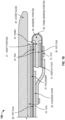
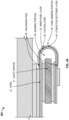
- FIGS. 1A-1C illustrate embodiments of a flexible display which may be incorporated in electronic devices.
- FIG. 1A illustrates an isometric view of a flexible display 100.
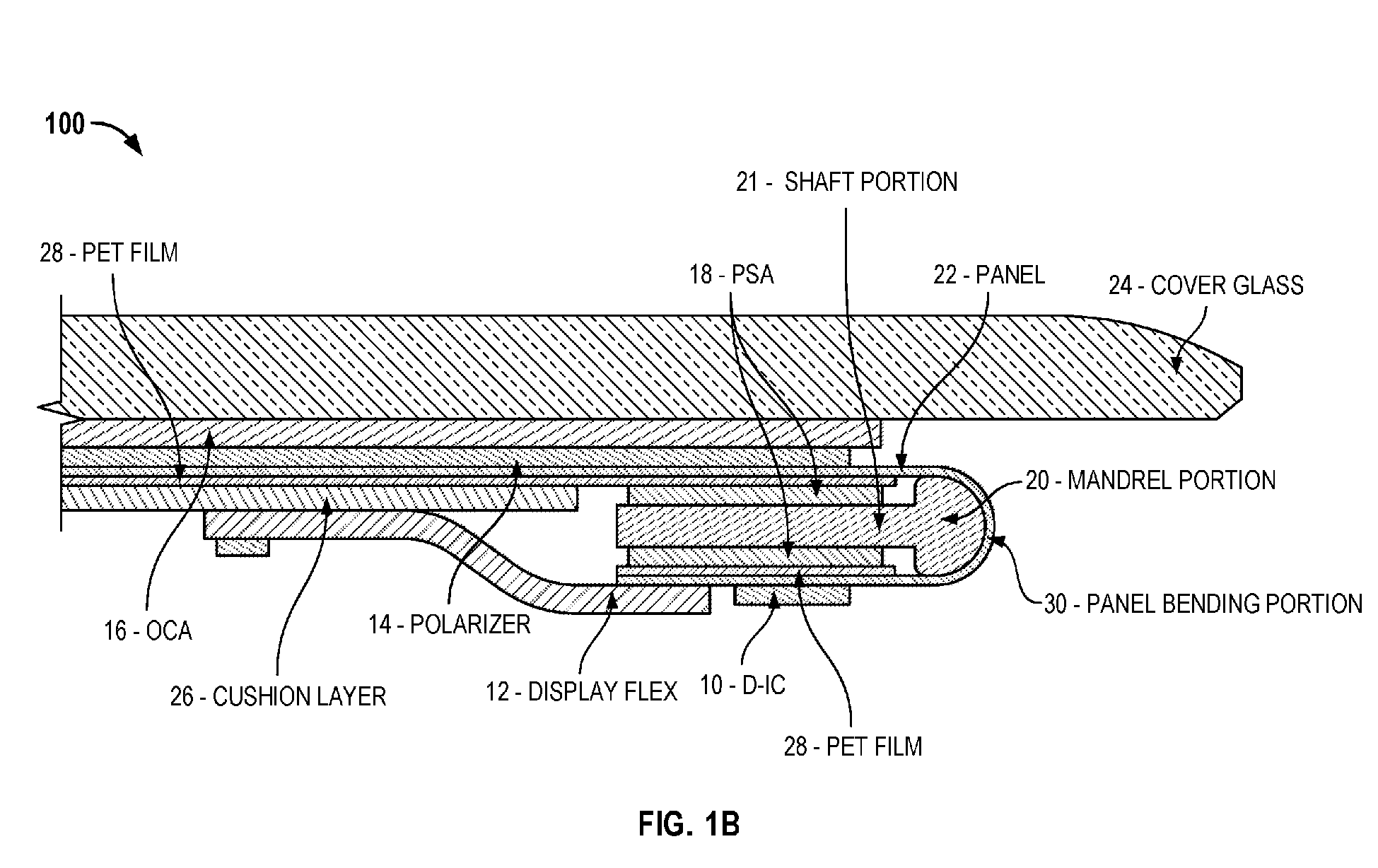
- FIG. 1B illustrates a side view of the flexible display 100.
- FIG. 1C illustrates a side view of a flexible display 150.
- Flexible displays 100 and 150 are substantially similar to one another and illustrate different embodiments of a mandrel portion 20 and a shaft portion 21 (see the description of FIGS. 1A-1C below for more detail).
- the flexible displays 100 and 150 include D-IC 10, display flex 12, polarizer 14, optically clear adhesive (OCA) 16, pressure-sensitive adhesive 18, mandrel portion 20, shaft portion 21, panel 22, cover glass 24, cushion layer 26, polyethylene terephthalate (PET) film 28, and panel bending portion 30.
- the D-IC 10 provides an interface function between a microprocessor, a microcontroller, an application-specific integrated circuit chips (ASIC), or a general-purpose peripheral interface and the flexible display 100 or 150.
- ASIC application-specific integrated circuit chips
- the D-IC 10 accepts commands and/or other types of data using a general-purpose serial or parallel interface, such as transistor-transistor logic (TTL), complementary metal-oxide-semiconductor (CMOS), recommended standard 232 (RS232), serial peripheral interface (SPI), inter-integrated circuit (I2C) and so forth.
- TTL transistor-transistor logic
- CMOS complementary metal-oxide-semiconductor
- RS232 recommended standard 232
- SPI serial peripheral interface
- I2C inter-integrated circuit
- the D-IC 10 generates signals with suitable voltage, current, timing, and demultiplexing to cause the flexible display (e.g., 100 or 150) to display or otherwise show the desired text and/or image.
- the D-IC 10 comprises an application-specific microcontroller and may incorporate random-access memory (RAM), flash memory, electrically erasable programmable read-only memory (EEPROM) and/or read only memory (ROM), which may be a fixed ROM that includes firmware and/or display fonts.
- RAM random-access memory
- EEPROM electrically erasable programmable read-only memory
- ROM read only memory
- the display flex 12 may be employed to connect data and power between, for example, the system and the display panel 22.
- display flex 12 is a PI based, flexible printed circuit board.
- the Polarizer 14 comprises an optical filter that allows light waves of a specific polarization to pass through while blocking light waves of other polarizations.
- the polarizer 14 can convert a beam of light of undefined or mixed polarization into a beam of well-defined polarization that is polarized light.
- PSA 14 is used for anti-reflection and sun glass readability for organic light emitting diodes (OLED) displays.
- the Polarizer 14 may be produced by venders such as, for example, 3M TM , Nitto TM , and Sumitomo TM .
- OCA 16 comprises a layer of an optically clear adhesive that is used to attach the cover glass 24 and the polarizer 14.
- OCA 16 may be produced by venders such as, for example, 3M TM , Nitto TM , and Mitsubishi TM .
- PSA 18 bonds the PET film 28 to the shaft portion 21.
- PSA 18 is an adhesive which forms a bond when pressure is applied to marry the adhesive with the adherend (e.g., the surfaces of shaft portion 21 and the PET film 28).
- PSA 18 forms a bond that holds at room temperatures.
- the mandrel portion 20 and the shaft portion 21 can be used to help form the shape of panel bending portion 30.
- the mandrel portion 20 and the shaft portion 21 may be portions of the same component and may be comprised of a thermoplastic or thermosoftening plastic, such as polycarbonate- Acrylonitrile Butadiene Styrene (ABS).
- ABS polycarbonate- Acrylonitrile Butadiene Styrene
- Thermoplastic is a plastic material or a polymer that becomes pliable and/or moldable above a specific temperature and solidifies upon cooling.
- the shaft portion 21 can be an element that is formed of a material and the mandrel portion 20 can be empty space.
- the shaft portion may be comprised of a foam material, such as polyurethane.
- the panel 22 is comprised of a conductive material, such as copper or aluminum alloy.
- the panel 22 may also include a substrate (not shown) that is comprised of PI (e.g., plastic) and includes an active area where, for example, images are displayed.
- PI e.g., plastic
- the panel 22 can be wrapped around the mandrel portion 20 and the shaft portion 21 to form panel bending portion 30. Once wrapped, the panel 22 can be adhered to the shaft portion 21 with the PSA 18.
- the PET film 28 is applied to the surface of the panel 22 that wraps around the shaft portion 21.
- PSA 18 bonds the shaft portion 21 to the PET film 28 that is applied to the inside surface of panel 22.
- the layers of the formed panel bending portion 30 are shown in greater detail in FIGS. 2-4C .
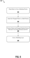
- FIG. 5 depicts a flow diagram of an example process (500) employed to manufacture a flexible display as described above.
- the first step in the described process wraps (502) a panel, such as panel 22, around a mandrel portion, such as mandrel portion 20, to form a bending portion of the panel.
- the next step in the process attaches (504) the wrapped panel on either side of a shaft portion, such as shaft portion 21.
- the next step positions (506) the panel and wrapped mandrel portion between a cover glass element, such as cover glass 24, and a D-IC, such as D-IC 10.
- the flexible display apparatus may further comprise coating layer over the shielding layer.
- the coating layer may have an opening exposing a portion of the shielding layer.
- the coating layer may comprise a polyimide substrate.
- the flexible display apparatus may further comprise a second coating layer, wherein the second coating layer is positioned between the shielding layer and the inner panel layer.
- the coating layer and the shielding layer may be layers of a conductive tape positioned around the second coating layer.
- the conductive tape may have a thickness between 10 pm and 100 pm.
- the second coating layer may have a thickness of between 100 pm to 50 pm.
- the inner panel layer may comprise a conductive material
- the shielding layer may comprise a second conductive material
- the panel may be attached to either side of the shaft portion with pressure sensitive adhesive.
- the shielding layer may comprise a thin conductive layer deposited by sputtering or printing over the bending portion of the panel, and the shielding layer may have a thickness of between 5 pm and 20 pm.
- the shaft portion may comprise a foam material, and the mandrel portion may comprise an empty space.
- the shaft portion and the mandrel portion may be portions of a same component, and the same component may comprise a plastic material.
- the plastic material may comprise a thermosoftening plastic.
- Also disclosed herein is a method of forming a mobile communication device flexible display apparatus comprising:
- the method may comprise, before forming the shielding layer, positioning at least two grounding pads on the bending portion and on opposite sides of the mandrel portion.
- the method may comprise forming a coating layer over the shielding layer.
- the method may further comprise forming an opening in the coating layer to expose a portion of the shielding layer.
- the method may further comprise, before forming the shielding layer, forming a second coating layer positioned around the bending portion of the panel, wherein the shielding layer is formed around the second coating layer.
- a mobile communication device comprising:
- Also disclosed herein is a mobile communication device comprising a flexible display apparatus as recited above.
Landscapes
- Engineering & Computer Science (AREA)
- Computer Hardware Design (AREA)
- Theoretical Computer Science (AREA)
- General Engineering & Computer Science (AREA)
- Physics & Mathematics (AREA)
- Microelectronics & Electronic Packaging (AREA)
- Human Computer Interaction (AREA)
- General Physics & Mathematics (AREA)
- Signal Processing (AREA)
- Electromagnetism (AREA)
- Devices For Indicating Variable Information By Combining Individual Elements (AREA)
- Shielding Devices Or Components To Electric Or Magnetic Fields (AREA)
Abstract

Description
- This disclosure generally relates to electronic devices, and, more particularly, a method for shielding a bending portion of a flexible display panel of an electronic device.
- Consumer electronics are equipment for everyday use and include devices for entertainment, such as gaming devices; communications, such as cell phones; and home office use, such as personal computers. As consumer electronics internal modules becomes more integrated, and thus more compact, the need for electrometric shielding between components becomes more critical.
- Implementations of the present disclosure are generally directed to a flexible display apparatus employed within, for example, a mobile communication device. More specifically, implementations are directed to a flexible display apparatus and methods of forming the flexible display apparatus. The flexible display apparatus includes a shielding layer at a bending portion of a panel of the display, which prevents or inhibits electromagnetic interference in this area of the device.
- In a general implementation, a mobile communication device includes: a cover glass element; a driver integrated circuit (D-IC); a mandrel portion; a shaft portion; a panel, positioned between the cover glass element and the D-IC, and comprising an inner panel layer that wraps around at least a portion of the mandrel portion to form a bending portion of the panel, the panel attached on either side on the shaft portion; and a shielding layer positioned around the inner panel layer and configured to inhibit electromagnetic signals through the bending portion.
- In another general implementation, a flexible display apparatus includes a cover glass element; a D-IC; a mandrel portion; a shaft portion; a panel, positioned between the cover glass element and the D-IC, and comprising an inner panel layer that wraps around at least a portion of the mandrel portion to form a bending portion of the panel, the panel attached on either side on the shaft portion; and a shielding layer positioned around the inner panel layer and configured to inhibit electromagnetic signals through the bending portion.
- In yet another general implementation, a method of forming a mobile communication device flexible display apparatus includes: wrapping a panel around a mandrel portion to form a bending portion of the panel; attaching the wrapped panel on either side of a shaft portion; positioning the panel and wrapped mandrel portion between a cover glass element and a D-IC; and forming a shielding layer positioned around the bending portion of the panel, the shielding layer configured to inhibit electromagnetic signals through the bending portion.
- In an aspect combinable with any of the general implementations, the flexible display apparatus, further comprising a coating layer over the shielding layer.
- In another aspect combinable with any of the previous aspects, further comprising at least two grounding pads positioned between the inner panel layer and the shielding layer and on opposite sides of the mandrel portion.
- Another aspect combinable with any of the previous aspects, the coating layer has an opening exposing a portion of the shielding layer.
- In another aspect combinable with any of the previous aspects, the coating layer comprises a polyimide (PI) substrate.
- In another aspect combinable with any of the previous aspects, further comprising a second coating layer, wherein the second coating layer is positioned between the shielding layer and the inner panel layer.
- In another aspect combinable with any of the previous aspects, the coating layer and the shielding layer are layers of a conductive tape positioned around the second coating layer.
- In another aspect combinable with any of the previous aspects, the conductive tape has a thickness between 10 micrometers (µm) and 100 µm, and wherein the second coating layer has a thickness of between 100 µm to 50 µm.
- In another aspect combinable with any of the previous aspects, the inner panel layer comprises a conductive material.
- Another aspect combinable with any of the previous aspects, the shielding layer comprises a second conductive material.
- Another aspect combinable with any of the previous aspects, the panel is attached to either side of the shaft portion with pressure sensitive adhesive.
- In another aspect combinable with any of the previous aspects, the shielding layer comprises a thin conductive layer deposited by sputtering or printing over the bending portion of the panel.
- In another aspect combinable with any of the previous aspects, the shielding layer has a thickness of between 5 µm and 20 µm.
- In another aspect combinable with any of the previous aspects, the shaft portion comprises a foam material, and wherein the mandrel portion comprises an empty space.
- In another aspect combinable with any of the previous aspects, the shaft portion and the mandrel portion are portions of a same component, and wherein the same component comprises a plastic material.
- In another aspect combinable with any of the previous aspects, the plastic material comprises a thermosoftening plastic.
- Integrating shielding at a display module level provides, for example, increased effectiveness because the shielding is close to a source of electromagnetic interference. The shielding also saves internal space compared with added shielding at a system level.
- The details of one or more implementations of the present disclosure are set forth in the accompanying drawings and the description below. Other features and advantages of the present disclosure will be apparent from the description and drawings, and from the claims.
-
-
FIGS. 1A-1C illustrate embodiments of a flexible display which may be incorporated in electronic devices. -
FIGS. 2 ,3A-3B , and4A-4C illustrate various embodiments of a panel bending portion of a flexible display with an added shielding layer at the bending. -
FIG. 5 depicts a flow diagram of an example process employed to manufacture a flexible display. - A display in a consumer electronic device may have a cushion layer, which includes a layer comprised of a conductive material, such as copper. This cushion layer can be used for shielding from a panel backside. The display may include a bending portion/region around a mandrel. In some implementations, the panel has one layer of polyimide substrate and one metal trace layer at the bending portion. This bending portion, however, may not be shielded. Such a lack of shielding at the bending portion can allow electromagnetic interference to antennas and/or cause desense issues.
- In view of the foregoing, implementations of the present disclosure are generally directed to a method and apparatus for shielding a bending portion of a flexible display that can be incorporated in electronic devices, such as a consumer electronic module. In some implementations, the described method adds a second or outer metal trace layer at the bending portion. In some implementations, the described method may also add a second polyimide substrate. In some implementations, the second metal trace layer can be utilized as a shielding layer, while the inner metal trace layer can be used for data, power, and so forth. For example, the shielding layer (e.g., the second metal trace layer) prevents and/or inhibits electromagnetic interference and other desense issues in this area of the device. For example, the shielding layer may prevent or inhibit electromagnetic interference to an antenna employed by a device that is comprised of the described flexible display.
-
FIGS. 1A-1C illustrate embodiments of a flexible display which may be incorporated in electronic devices.FIG. 1A illustrates an isometric view of aflexible display 100.FIG. 1B illustrates a side view of theflexible display 100.FIG. 1C illustrates a side view of aflexible display 150.Flexible displays mandrel portion 20 and a shaft portion 21 (see the description ofFIGS. 1A-1C below for more detail). - The
flexible displays display flex 12,polarizer 14, optically clear adhesive (OCA) 16, pressure-sensitive adhesive 18,mandrel portion 20,shaft portion 21,panel 22,cover glass 24, cushion layer 26, polyethylene terephthalate (PET)film 28, andpanel bending portion 30. In some implementations, the D-IC 10 provides an interface function between a microprocessor, a microcontroller, an application-specific integrated circuit chips (ASIC), or a general-purpose peripheral interface and theflexible display IC 10 accepts commands and/or other types of data using a general-purpose serial or parallel interface, such as transistor-transistor logic (TTL), complementary metal-oxide-semiconductor (CMOS), recommended standard 232 (RS232), serial peripheral interface (SPI), inter-integrated circuit (I2C) and so forth. In some implementations, the D-IC 10 generates signals with suitable voltage, current, timing, and demultiplexing to cause the flexible display (e.g., 100 or 150) to display or otherwise show the desired text and/or image. In some implementations, the D-IC 10 comprises an application-specific microcontroller and may incorporate random-access memory (RAM), flash memory, electrically erasable programmable read-only memory (EEPROM) and/or read only memory (ROM), which may be a fixed ROM that includes firmware and/or display fonts. - The
display flex 12 may be employed to connect data and power between, for example, the system and thedisplay panel 22. In some implementations,display flex 12 is a PI based, flexible printed circuit board. In some implementations, thePolarizer 14 comprises an optical filter that allows light waves of a specific polarization to pass through while blocking light waves of other polarizations. For example, thepolarizer 14 can convert a beam of light of undefined or mixed polarization into a beam of well-defined polarization that is polarized light. In some implementations,PSA 14 is used for anti-reflection and sun glass readability for organic light emitting diodes (OLED) displays. ThePolarizer 14 may be produced by venders such as, for example, 3M™, Nitto™, and Sumitomo™. In some implementations,OCA 16 comprises a layer of an optically clear adhesive that is used to attach thecover glass 24 and thepolarizer 14.OCA 16 may be produced by venders such as, for example, 3M™, Nitto™, and Mitsubishi™. - In some implementations,
PSA 18 bonds thePET film 28 to theshaft portion 21. In some implementations,PSA 18 is an adhesive which forms a bond when pressure is applied to marry the adhesive with the adherend (e.g., the surfaces ofshaft portion 21 and the PET film 28). In some implementations,PSA 18 forms a bond that holds at room temperatures. - In some implementations, the
mandrel portion 20 and theshaft portion 21 can be used to help form the shape ofpanel bending portion 30. As shown inFIGS. 1A and1B , themandrel portion 20 and theshaft portion 21 may be portions of the same component and may be comprised of a thermoplastic or thermosoftening plastic, such as polycarbonate- Acrylonitrile Butadiene Styrene (ABS). Thermoplastic is a plastic material or a polymer that becomes pliable and/or moldable above a specific temperature and solidifies upon cooling. As shown inFIG. 1C , theshaft portion 21 can be an element that is formed of a material and themandrel portion 20 can be empty space. In such embodiments, the shaft portion may be comprised of a foam material, such as polyurethane. - In some implementations, the
panel 22 is comprised of a conductive material, such as copper or aluminum alloy. Thepanel 22 may also include a substrate (not shown) that is comprised of PI (e.g., plastic) and includes an active area where, for example, images are displayed. - As shown in
FIGS. 1A-1C , thepanel 22 can be wrapped around themandrel portion 20 and theshaft portion 21 to formpanel bending portion 30. Once wrapped, thepanel 22 can be adhered to theshaft portion 21 with thePSA 18. In some implementations, thePET film 28 is applied to the surface of thepanel 22 that wraps around theshaft portion 21. In such implementations,PSA 18 bonds theshaft portion 21 to thePET film 28 that is applied to the inside surface ofpanel 22. The layers of the formedpanel bending portion 30 are shown in greater detail inFIGS. 2-4C . - The cushion layer 26 protects
panel 22 and provides electrical grounding and thermal dissipation. In some implementations, the cushion layer 26 is comprised of adhesion, foam, and conductive (e.g., copper) layers. Thecover glass 24 is a top layer offlexible displays 100 and 150 (e.g., the screen) and may be comprised of a hard or toughened glass, such as aluminosilicate glass. Toughened glass is designed to resist shattering and scratching. -
FIGS. 2 ,3A-B , and4A-4C illustrate various embodiments of thepanel bending portion 30 offlexible displays mandrel portion 20 andshaft portion 21 are illustrated as they are depicted in flexible display 150 (e.g., with an empty or air filled mandrel portion 20); however, other embodiments include themandrel portion 20 andshaft portion 21 comprising a single element, such as illustrated in flexible display 100 (as shown inFIGS. 1A and1B ). -
FIG. 2 illustrates a side view of anembodiment 200 of a double layer panel bending, with a shielding layer at the bending. As depicted, thepanel bending portion 30 is an element of a flexible display, such asflexible displays embodiment 200 includespanel 22,shaft portion 21,mandrel portion 20, andpanel bending portion 30, as shown inflexible display 150. As depicted, thepanel bending portion 30 includesinner panel layer 32,outer layer panel 34,coating layer 36, and grounding pads orvias 40. - In some implementations, the
inner panel layer 32 and theouter layer panel 34 are metal trace layers comprised of a conductive material, such as copper or aluminum. Thecoating layer 36 prevents moisture ingression and adjusts locations of stress in the panel member at the panel bending 30. Thecoating layer 36 may be comprised of a curable epoxy, such as Loctitie. In some implementations, thecoating layer 36 is 10 µm~100 µm thick and theinner panel layer 32 has a submicron thickness. - In the depicted example, the
grounding pads 40 are embedded in panel 22 (in the inner panel layer 32). Groundingpads 40 may be employed to electrically connect theouter layer panel 34 to the inner panel layer 32 (e.g., the metal trace) inside of thepanel 22. -
FIGS. 3A-3B illustrate respectively a side view ofembodiments panel bending portion 30 in which conductive tape or foil is attached over the bending. As depicted, thepanel bending portion 30 is an element of a flexible display, such asflexible displays embodiments panel 22,shaft portion 21,mandrel portion 20, andpanel bending portion 30 as shown inflexible display 150. Thepanel bending portion 30 includesinner panel layer 32,coating layer 36,conductive tape layer 35, andinsulation layer 37.Inner panel layer 32 andcoating layer 36 are substantially similar to the same components ofembodiment 200. In some implementations, the applied conductive tape or foil includesconductive layer 35 andinsulation layer 37, which form layers of thepanel bending portion 30 once the panel is bent around the shaft and mandrel portions. - In some implementations, the conductive tape is 10 µm ∼100 µm thick. The conductive tape may be added to the
panel 22 before the bending process takes place and after thecoating layer 36 is applied to thepanel 22. The conductive tape may be attached to thepanel 22 by a conductive PSA, and then bent together withpanel 22 during a bending process to formpanel bending portion 30. Inembodiments coating layer 36 may be thinner (from 100 µm to 50 µm) than the coating inembodiment 200 ofFIG. 2 because of the added extra shielding layer (e.g., conductive tape layer 35). In some implementations, thecoating layer 36 may be removed completely and replaced by theconductive tape layer 35 andinsulation tape layer 37. - As depicted in
FIG. 3A ,embodiment 300 includes grounding pads orvias 40, which are embedded in panel 22 (in the inner panel layer 32). Groundingpads 40 are substantially similar to the same components ofembodiment 200 and may be employed to electrically connect theconductive tape layer 35 to the inner panel layer 32 (e.g., the metal trace) inside of thepanel 22. Alternatively, as depicted inFIG. 3B ,embodiment 350 includesopening 44. In some implementations, theopening 44 is formed in theinsulation tape layer 37 to expose a portion of theconductive tape layer 35. In such implementations, the portion ofconductive tape layer 35 exposed by theopening 44 may be employed to connect to the system ground for shielding, by, for example, a conductive PSA, paste, or spring finger. -
FIGS. 4A-4C illustrates respectively a side view ofembodiments panel bending portion 30 in which a thin layer of conductive material, such as copper or aluminum, is deposited by sputtering or printing over a layer of thepanel bending portion 30. As depicted,panel bending portion 30 is an element of a flexible display, such asflexible displays embodiments panel 22,shaft portion 21,mandrel portion 20, andpanel bending portion 30, as shown inflexible display 150. - As depicted in
FIG. 4A ,embodiment 400 comprises apanel bending portion 30 that includesinner panel layer 32,coating layer 36, and conductive sputteredlayer 38.Inner panel layer 32 andcoating layer 36 are substantially similar to the same components ofembodiment layer 38 is deposited as a shielding layer at thepanel bending portion 30 by sputtering or printing the conductive material inside of the coating layer 36 (e.g., before thecoating layer 36 is applied) and over theinner panel layer 32. In some implementations, the conductive sputteredlayer 38 is applied to a thickness of between 5 µm ~20 µm. - As depicted in
FIGS. 4B and4C ,embodiments panel bending portion 30 that includesinner panel layer 32,coating layer 36, conductive sputteredlayer 38, andinsulation tape layer 37.Inner panel layer 32 andcoating layer 36 are substantially similar to the same components ofembodiment layer 38 is deposited as a shielding layer at thepanel bending portion 30 by sputtering or printing the conductive material over the coating layer 36 (e.g., after thecoating layer 36 is applied). In some implementations, the conductive sputteredlayer 38 is applied to a thickness of between 5 µm ~20 µm. Insulatingtape layer 37 is added over the conductive sputteredlayer 38. In some implementations, insulatingtape layer 37 is comprised of polyester or PI. - As depicted in
FIGS. 4A and4B ,embodiments vias 40, which are embedded in panel 22 (in the inner panel layer 32). Groundingpads 40 are substantially similar to the same components ofembodiment coating layer 36 as depicted inembodiment 400 or outside of thecoating layer 36 as depicted in embodiment 450) to the inner panel layer 32 (e.g., the metal trace) inside of thepanel 22. Alternatively, as depicted inFIG. 4C ,embodiment 470 includesopening 44. Similar toembodiment 350 inFIG. 3B , theopening 44 is formed in theinsulation tape layer 37 to expose a portion of the conductive sputteredlayer 38. In some implementations, the portion ofconductive tape layer 35 exposed by theopening 44 may be employed to connect to the system ground for shielding, by, for example, a conductive PSA, paste, or spring finger. -
FIG. 5 depicts a flow diagram of an example process (500) employed to manufacture a flexible display as described above. The first step in the described process wraps (502) a panel, such aspanel 22, around a mandrel portion, such asmandrel portion 20, to form a bending portion of the panel. The next step in the process attaches (504) the wrapped panel on either side of a shaft portion, such asshaft portion 21. The next step positions (506) the panel and wrapped mandrel portion between a cover glass element, such ascover glass 24, and a D-IC, such as D-IC 10. The next step in the process forms (508) a shielding layer, such asouter layer panel 34,conductive tape layer 35, or conductive sputteredlayer 38, positioned around the bending portion of the panel. The shielding layer is configured to inhibit electromagnetic signals through the bending portion. - Also disclosed herein is a flexible display apparatus, comprising:
- a cover glass element;
- a driver integrated circuit;
- a mandrel portion;
- a shaft portion;
- a panel, positioned between the cover glass element and the driver integrated circuit, and comprising an inner panel layer that wraps around at least a portion of the mandrel portion to form a bending portion of the panel, the panel attached on either side on the shaft portion; and
- a shielding layer positioned around the inner panel layer and configured to inhibit electromagnetic signals through the bending portion.
- The flexible display apparatus may further comprise at least two grounding pads positioned between the inner panel layer and the shielding layer and on opposite sides of the mandrel portion.
- The flexible display apparatus may further comprise coating layer over the shielding layer.
- The coating layer may have an opening exposing a portion of the shielding layer.
- The coating layer may comprise a polyimide substrate.
- The flexible display apparatus may further comprise a second coating layer, wherein the second coating layer is positioned between the shielding layer and the inner panel layer.
- The coating layer and the shielding layer may be layers of a conductive tape positioned around the second coating layer.
- The conductive tape may have a thickness between 10 pm and 100 pm. The second coating layer may have a thickness of between 100 pm to 50 pm.
- The inner panel layer may comprise a conductive material, and the shielding layer may comprise a second conductive material.
- The panel may be attached to either side of the shaft portion with pressure sensitive adhesive.
- The shielding layer may comprise a thin conductive layer deposited by sputtering or printing over the bending portion of the panel, and the shielding layer may have a thickness of between 5 pm and 20 pm.
- The shaft portion may comprise a foam material, and the mandrel portion may comprise an empty space.
- The shaft portion and the mandrel portion may be portions of a same component, and the same component may comprise a plastic material.
- The plastic material may comprise a thermosoftening plastic.
- Also disclosed herein is a method of forming a mobile communication device flexible display apparatus comprising:
- wrapping a panel around a mandrel portion to form a bending portion of the panel;
- attaching the wrapped panel on either side of a shaft portion;
- positioning the panel and wrapped mandrel portion between a cover glass element and a driver integrated circuit; and
- forming a shielding layer positioned around the bending portion of the panel, the shielding layer configured to inhibit electromagnetic signals through the bending portion.
- The method may comprise, before forming the shielding layer, positioning at least two grounding pads on the bending portion and on opposite sides of the mandrel portion.
- The method may comprise forming a coating layer over the shielding layer.
- The method may further comprise forming an opening in the coating layer to expose a portion of the shielding layer.
- The method may further comprise, before forming the shielding layer, forming a second coating layer positioned around the bending portion of the panel, wherein the shielding layer is formed around the second coating layer.
- Also disclosed herein is a mobile communication device, comprising:
- a cover glass element;
- a driver integrated circuit;
- a mandrel portion;
- a shaft portion;
- a panel, positioned between the cover glass element and the driver integrated circuit, and comprising an inner panel layer that wraps around at least a portion of the mandrel portion to form a bending portion of the panel, the panel attached on either side on the shaft portion; and a shielding layer positioned around the inner panel layer and configured to inhibit electromagnetic signals through the bending portion.
- Also disclosed herein is a mobile communication device comprising a flexible display apparatus as recited above.
- While this specification contains many specific implementation details, these should not be construed as limitations on the scope of any inventions or of what may be claimed, but rather as descriptions of features specific to particular implementations of particular inventions. Certain features that are described in this specification in the context of separate implementations can also be implemented in combination in a single implementation. Conversely, various features that are described in the context of a single implementation can also be implemented in multiple implementations separately or in any suitable subcombination. Moreover, although features may be described above as acting in certain combinations and even initially claimed as such, one or more features from a claimed combination can in some cases be excised from the combination, and the claimed combination may be directed to a subcombination or variation of a subcombination.
- Similarly, while operations are depicted in the drawings in a particular order, this should not be understood as requiring that such operations be performed in the particular order shown or in sequential order, or that all illustrated operations be performed, to achieve desirable results. In certain circumstances, multitasking and parallel processing may be advantageous. Moreover, the separation of various system components in the implementations described above should not be understood as requiring such separation in all implementations, and it should be understood that the described program components and systems can generally be integrated together in a single software product or packaged into multiple software products.
- Thus, particular implementations of the subject matter have been described. Other implementations are within the scope of the following claims. In some cases, the actions recited in the claims can be performed in a different order and still achieve desirable results. In addition, the processes depicted in the accompanying figures do not necessarily require the particular order shown, or swequential order, to achieve desirable results. In certain implementations, multitasking and parallel processing may be advantageous.
Claims (14)
- A flexible display apparatus, comprising:a cover glass element;a driver integrated circuit;a mandrel portion;a shaft portion;a panel, positioned between the cover glass element and the driver integrated circuit, and comprising an inner panel layer that wraps around at least a portion of the mandrel portion to form a bending portion of the panel, the panel attached on either side on the shaft portion;a shielding layer positioned around the inner panel layer and configured to inhibit electromagnetic signals through the bending portion; anda coating layer over the shielding layer.
- The flexible display apparatus of claim 1, further comprising at least two grounding pads positioned between the inner panel layer and the shielding layer and on opposite sides of the mandrel portion.
- The flexible display apparatus of claim 1 or 2, wherein the coating layer has an opening exposing a portion of the shielding layer.
- The flexible display apparatus of any one of the preceding claims, wherein the coating layer comprises a polyimide substrate.
- The flexible display apparatus of any preceding claim, wherein the inner panel layer comprises a conductive material, and wherein the shielding layer comprises a second conductive material.
- The flexible display apparatus of any preceding claim, wherein the panel is attached to either side of the shaft portion with pressure sensitive adhesive.
- The flexible display apparatus of any preceding claim, wherein the shielding layer comprises a thin conductive layer deposited by sputtering or printing over the bending portion of the panel, and wherein the shielding layer has a thickness of between 5 pm and 20 pm.
- The flexible display apparatus of any preceding claim, wherein the shaft portion comprises a foam material, and wherein the mandrel portion comprises an empty space.
- The flexible display apparatus of any preceding claim, wherein the shaft portion and the mandrel portion are portions of a same component, and wherein the same component comprises a plastic material.
- The flexible display apparatus of claim 9, wherein the plastic material comprises a thermosoftening plastic.
- A mobile communication device comprising a flexible display apparatus as claimed in any of claims 1 to 10.
- A method of forming a mobile communication device flexible display apparatus comprising:wrapping a panel around a mandrel portion to form a bending portion of the panel;attaching the wrapped panel on either side of a shaft portion;positioning the panel and wrapped mandrel portion between a cover glass element and a driver integrated circuit;forming a shielding layer positioned around the bending portion of the panel, the shielding layer configured to inhibit electromagnetic signals through the bending portion; andforming a coating layer over the shielding layer.
- The method of either of claim 12, further comprising before forming the shielding layer, positioning at least two grounding pads on the bending portion and on opposite sides of the mandrel portion.
- The method of claim 13, further comprising forming an opening in the coating layer to expose a portion of the shielding layer.
Applications Claiming Priority (3)
| Application Number | Priority Date | Filing Date | Title |
|---|---|---|---|
| US201762594915P | 2017-12-05 | 2017-12-05 | |
| EP18826147.3A EP3602236B1 (en) | 2017-12-05 | 2018-11-27 | Shielding a bending portion of a flexible display |
| PCT/US2018/062550 WO2019112836A1 (en) | 2017-12-05 | 2018-11-27 | Shielding a bending portion of a flexible display |
Related Parent Applications (1)
| Application Number | Title | Priority Date | Filing Date |
|---|---|---|---|
| EP18826147.3A Division EP3602236B1 (en) | 2017-12-05 | 2018-11-27 | Shielding a bending portion of a flexible display |
Publications (2)
| Publication Number | Publication Date |
|---|---|
| EP4482130A2 true EP4482130A2 (en) | 2024-12-25 |
| EP4482130A3 EP4482130A3 (en) | 2025-02-26 |
Family
ID=64870571
Family Applications (2)
| Application Number | Title | Priority Date | Filing Date |
|---|---|---|---|
| EP18826147.3A Active EP3602236B1 (en) | 2017-12-05 | 2018-11-27 | Shielding a bending portion of a flexible display |
| EP24203984.0A Pending EP4482130A3 (en) | 2017-12-05 | 2018-11-27 | Shielding a bending portion of a flexible display |
Family Applications Before (1)
| Application Number | Title | Priority Date | Filing Date |
|---|---|---|---|
| EP18826147.3A Active EP3602236B1 (en) | 2017-12-05 | 2018-11-27 | Shielding a bending portion of a flexible display |
Country Status (4)
| Country | Link |
|---|---|
| US (2) | US10602645B2 (en) |
| EP (2) | EP3602236B1 (en) |
| CN (1) | CN110692029B (en) |
| WO (1) | WO2019112836A1 (en) |
Families Citing this family (19)
| Publication number | Priority date | Publication date | Assignee | Title |
|---|---|---|---|---|
| KR102504397B1 (en) * | 2018-08-20 | 2023-03-02 | 삼성디스플레이 주식회사 | Display device and method for fabricating electronic device using the same |
| KR102555954B1 (en) * | 2018-08-31 | 2023-07-19 | 삼성디스플레이 주식회사 | Display device |
| KR102524236B1 (en) * | 2018-11-16 | 2023-04-24 | 삼성전자주식회사 | Electric device including waterproof structure |
| KR102763209B1 (en) * | 2019-07-01 | 2025-02-07 | 삼성전자주식회사 | Electronic device incuding glass plate |
| CN112817471B (en) * | 2019-11-18 | 2024-09-06 | 北京小米移动软件有限公司 | Flexible screen, terminal equipment and manufacturing method of flexible screen |
| KR102925181B1 (en) * | 2020-01-10 | 2026-02-09 | 삼성디스플레이 주식회사 | Display device |
| KR102806184B1 (en) * | 2020-02-07 | 2025-05-13 | 삼성전자주식회사 | Electronic device including printing film |
| US11563189B2 (en) * | 2020-03-06 | 2023-01-24 | Samsung Display Co., Ltd | Display device including bending protection and anti-reflection layers |
| CN111668275A (en) * | 2020-06-19 | 2020-09-15 | 京东方科技集团股份有限公司 | Display panel, method of making the same, and display device |
| CN112310671B (en) * | 2020-07-27 | 2022-04-12 | 深圳市卓汉材料技术有限公司 | High-temperature-resistant grounding elastic piece and electronic equipment |
| US11800649B2 (en) * | 2020-08-19 | 2023-10-24 | Apple Inc. | Mobile display encapsulation to improve robustness and water resistance |
| KR102827510B1 (en) | 2020-12-24 | 2025-06-30 | 엘지디스플레이 주식회사 | Display module and display device |
| EP4020074B1 (en) * | 2020-12-24 | 2025-04-02 | LG Display Co., Ltd. | Display device and display apparatus |
| KR102836941B1 (en) | 2020-12-24 | 2025-07-21 | 엘지디스플레이 주식회사 | Display module and display device |
| KR102819738B1 (en) * | 2020-12-24 | 2025-06-11 | 엘지디스플레이 주식회사 | Display module and display device |
| JP2023005541A (en) * | 2021-06-29 | 2023-01-18 | レノボ・シンガポール・プライベート・リミテッド | Electronic device |
| TWI824277B (en) * | 2021-08-06 | 2023-12-01 | 友達光電股份有限公司 | Display device and manufacturing method thereof |
| KR102938560B1 (en) * | 2021-10-05 | 2026-03-11 | 엘지디스플레이 주식회사 | Display apparatus and fabricating method of cushion plate |
| KR20230082223A (en) * | 2021-12-01 | 2023-06-08 | 엘지디스플레이 주식회사 | Display apparatus |
Family Cites Families (15)
| Publication number | Priority date | Publication date | Assignee | Title |
|---|---|---|---|---|
| JP4581726B2 (en) * | 2004-12-28 | 2010-11-17 | ソニー株式会社 | Display device and portable device |
| JP2009216753A (en) * | 2008-03-07 | 2009-09-24 | Hitachi Displays Ltd | Liquid crystal display device |
| US8456851B2 (en) * | 2008-05-16 | 2013-06-04 | Apple Inc. | Flex circuit with single sided routing and double sided attach |
| US8583187B2 (en) * | 2010-10-06 | 2013-11-12 | Apple Inc. | Shielding structures for wireless electronic devices with displays |
| JP5800507B2 (en) * | 2011-01-06 | 2015-10-28 | 株式会社ジャパンディスプレイ | Liquid crystal display |
| JP5687570B2 (en) * | 2011-06-10 | 2015-03-18 | 株式会社ジャパンディスプレイ | Display device |
| KR101855245B1 (en) * | 2011-07-13 | 2018-05-08 | 삼성전자 주식회사 | Touch screen panel active matrix organic light emitting diode display device |
| KR101942918B1 (en) * | 2012-05-03 | 2019-01-28 | 삼성전자주식회사 | Chip-on-film package and device assembly |
| KR101979361B1 (en) * | 2012-10-25 | 2019-05-17 | 삼성디스플레이 주식회사 | Chip on film and display device including the same |
| TWI489336B (en) * | 2012-11-22 | 2015-06-21 | Wintek Corp | Touch panel and touch display module thereof |
| KR102207839B1 (en) | 2014-10-14 | 2021-01-26 | 삼성디스플레이 주식회사 | Display device |
| US9706607B2 (en) * | 2014-12-10 | 2017-07-11 | Lg Display Co., Ltd. | Flexible display device with multiple types of micro-coating layers |
| US9535522B2 (en) * | 2014-12-22 | 2017-01-03 | Lg Display Co., Ltd. | Flexible organic light emitting diode display device |
| KR102275318B1 (en) * | 2015-03-02 | 2021-07-13 | 삼성디스플레이 주식회사 | Image display apparatus |
| KR102611214B1 (en) * | 2016-08-30 | 2023-12-07 | 삼성디스플레이 주식회사 | Display device and manufacturing method thereof |
-
2018
- 2018-11-27 EP EP18826147.3A patent/EP3602236B1/en active Active
- 2018-11-27 US US16/201,029 patent/US10602645B2/en active Active
- 2018-11-27 CN CN201880031333.7A patent/CN110692029B/en active Active
- 2018-11-27 WO PCT/US2018/062550 patent/WO2019112836A1/en not_active Ceased
- 2018-11-27 EP EP24203984.0A patent/EP4482130A3/en active Pending
-
2020
- 2020-02-12 US US16/788,968 patent/US10952356B2/en active Active
Also Published As
| Publication number | Publication date |
|---|---|
| EP4482130A3 (en) | 2025-02-26 |
| CN110692029A (en) | 2020-01-14 |
| WO2019112836A1 (en) | 2019-06-13 |
| US10952356B2 (en) | 2021-03-16 |
| US20200187395A1 (en) | 2020-06-11 |
| US10602645B2 (en) | 2020-03-24 |
| EP3602236A1 (en) | 2020-02-05 |
| US20190174658A1 (en) | 2019-06-06 |
| EP3602236B1 (en) | 2024-10-02 |
| CN110692029B (en) | 2024-02-06 |
Similar Documents
| Publication | Publication Date | Title |
|---|---|---|
| US10952356B2 (en) | Shielding portions of an electronic device | |
| US10485101B2 (en) | Flexible display device | |
| US10036734B2 (en) | Ultrasonic sensor with bonded piezoelectric layer | |
| US11029788B2 (en) | Display device including a force sensor | |
| US20110019370A1 (en) | Flexible circuit module | |
| US10061965B2 (en) | Fingerprint sensing unit and fingerprint sensing module | |
| CN112771598B (en) | Display device and assembly method thereof | |
| US11355687B2 (en) | Graphite-laminated chip-on-film-type semiconductor package having improved heat dissipation and electromagnetic wave shielding functions | |
| KR20140103761A (en) | Window assembly for display device including antenna and manufacturing method thereof | |
| CN117523981B (en) | Display modules and display devices | |
| US20120044414A1 (en) | Thin Image Capturing Apparatus | |
| KR20160099406A (en) | An electronic device including a circuit board | |
| EP3482387B1 (en) | Chip on film, flexible display apparatus having the same, and fabricating method thereof | |
| US20240213181A1 (en) | Display panel and display device | |
| CN205792909U (en) | Camera module | |
| CN222839908U (en) | Locking assembly, display module and display device | |
| KR102236034B1 (en) | Flexible display device | |
| KR101370604B1 (en) | Method of manufacturing display panel and partial masking tape for display panel | |
| US20250374805A1 (en) | Display module and method of manufacturing the display module | |
| CN210605515U (en) | Display panel and electronic device | |
| CN120547861A (en) | A wrapped conductive shielding film for SD memory cards | |
| CN118486236A (en) | Display module and display device | |
| CN119381389A (en) | Display module and display device |
Legal Events
| Date | Code | Title | Description |
|---|---|---|---|
| PUAI | Public reference made under article 153(3) epc to a published international application that has entered the european phase |
Free format text: ORIGINAL CODE: 0009012 |
|
| STAA | Information on the status of an ep patent application or granted ep patent |
Free format text: STATUS: THE APPLICATION HAS BEEN PUBLISHED |
|
| AC | Divisional application: reference to earlier application |
Ref document number: 3602236 Country of ref document: EP Kind code of ref document: P |
|
| AK | Designated contracting states |
Kind code of ref document: A2 Designated state(s): AL AT BE BG CH CY CZ DE DK EE ES FI FR GB GR HR HU IE IS IT LI LT LU LV MC MK MT NL NO PL PT RO RS SE SI SK SM TR |
|
| RIN1 | Information on inventor provided before grant (corrected) |
Inventor name: TAO, YI Inventor name: CHOI, WONJAE Inventor name: QI, QI |
|
| REG | Reference to a national code |
Ref country code: DE Ref legal event code: R079 Free format text: PREVIOUS MAIN CLASS: H04M0001020000 Ipc: G06F0001160000 |
|
| PUAL | Search report despatched |
Free format text: ORIGINAL CODE: 0009013 |
|
| AK | Designated contracting states |
Kind code of ref document: A3 Designated state(s): AL AT BE BG CH CY CZ DE DK EE ES FI FR GB GR HR HU IE IS IT LI LT LU LV MC MK MT NL NO PL PT RO RS SE SI SK SM TR |
|
| RIC1 | Information provided on ipc code assigned before grant |
Ipc: H05K 1/02 20060101ALI20250120BHEP Ipc: H04M 1/02 20060101ALI20250120BHEP Ipc: G06F 1/16 20060101AFI20250120BHEP |
|
| STAA | Information on the status of an ep patent application or granted ep patent |
Free format text: STATUS: REQUEST FOR EXAMINATION WAS MADE |
|
| 17P | Request for examination filed |
Effective date: 20250815 |