EP4482034A1 - High-voltage bidirectional switch device with improved electrical characteristics - Google Patents
High-voltage bidirectional switch device with improved electrical characteristics Download PDFInfo
- Publication number
- EP4482034A1 EP4482034A1 EP24179551.7A EP24179551A EP4482034A1 EP 4482034 A1 EP4482034 A1 EP 4482034A1 EP 24179551 A EP24179551 A EP 24179551A EP 4482034 A1 EP4482034 A1 EP 4482034A1
- Authority
- EP
- European Patent Office
- Prior art keywords
- turn
- transistor
- terminal
- switch
- terminal connected
- Prior art date
- Legal status (The legal status is an assumption and is not a legal conclusion. Google has not performed a legal analysis and makes no representation as to the accuracy of the status listed.)
- Pending
Links
Images

Classifications
-
- H—ELECTRICITY
- H03—ELECTRONIC CIRCUITRY
- H03K—PULSE TECHNIQUE
- H03K17/00—Electronic switching or gating, i.e. not by contact-making and –breaking
- H03K17/51—Electronic switching or gating, i.e. not by contact-making and –breaking characterised by the components used
- H03K17/74—Electronic switching or gating, i.e. not by contact-making and –breaking characterised by the components used by the use, as active elements, of diodes
-
- H—ELECTRICITY
- H03—ELECTRONIC CIRCUITRY
- H03K—PULSE TECHNIQUE
- H03K17/00—Electronic switching or gating, i.e. not by contact-making and –breaking
- H03K17/04—Modifications for accelerating switching
- H03K17/041—Modifications for accelerating switching without feedback from the output circuit to the control circuit
- H03K17/04106—Modifications for accelerating switching without feedback from the output circuit to the control circuit in field-effect transistor switches
-
- H—ELECTRICITY
- H03—ELECTRONIC CIRCUITRY
- H03K—PULSE TECHNIQUE
- H03K17/00—Electronic switching or gating, i.e. not by contact-making and –breaking
- H03K17/51—Electronic switching or gating, i.e. not by contact-making and –breaking characterised by the components used
- H03K17/56—Electronic switching or gating, i.e. not by contact-making and –breaking characterised by the components used by the use, as active elements, of semiconductor devices
- H03K17/687—Electronic switching or gating, i.e. not by contact-making and –breaking characterised by the components used by the use, as active elements, of semiconductor devices the devices being field-effect transistors
- H03K17/6871—Electronic switching or gating, i.e. not by contact-making and –breaking characterised by the components used by the use, as active elements, of semiconductor devices the devices being field-effect transistors the output circuit comprising more than one controlled field-effect transistor
-
- H—ELECTRICITY
- H03—ELECTRONIC CIRCUITRY
- H03K—PULSE TECHNIQUE
- H03K2217/00—Indexing scheme related to electronic switching or gating, i.e. not by contact-making or -breaking covered by H03K17/00
- H03K2217/0009—AC switches, i.e. delivering AC power to a load
-
- H—ELECTRICITY
- H03—ELECTRONIC CIRCUITRY
- H03K—PULSE TECHNIQUE
- H03K2217/00—Indexing scheme related to electronic switching or gating, i.e. not by contact-making or -breaking covered by H03K17/00
- H03K2217/0054—Gating switches, e.g. pass gates
-
- H—ELECTRICITY
- H03—ELECTRONIC CIRCUITRY
- H03K—PULSE TECHNIQUE
- H03K2217/00—Indexing scheme related to electronic switching or gating, i.e. not by contact-making or -breaking covered by H03K17/00
- H03K2217/0081—Power supply means, e.g. to the switch driver
-
- H—ELECTRICITY
- H03—ELECTRONIC CIRCUITRY
- H03K—PULSE TECHNIQUE
- H03K2217/00—Indexing scheme related to electronic switching or gating, i.e. not by contact-making or -breaking covered by H03K17/00
- H03K2217/009—Resonant driver circuits
Definitions
- the present solution relates to a high-voltage bidirectional switch device with improved electrical characteristics.
- bidirectional high-voltage switch devices capable of allowing the transfer of current in both directions between a first high-voltage terminal and a second high-voltage terminal.
- high-voltage switch devices are commonly used in charge recovery resonant drivers.
- These drivers base the charge recovery on a suitable sharing between a first and a second load capacitive elements (which may correspond to capacitive actuators, for example capacitive micromirrors) by using a certain number of tank and storage capacitors.
- a first and a second load capacitive elements which may correspond to capacitive actuators, for example capacitive micromirrors
- the sharing of charge between the capacitive elements is achieved according to a specific charge recovery algorithm by means of bidirectional switch devices connected between the same capacitive elements and the storage capacitors, suitably driven by driving signals having a high-voltage (of the order of several tens of V) and average frequencies (up to a few tens of kHz).
- switch devices are required to manage (bidirectionally) high voltages on both terminals.
- switch devices not only need to have low on-state resistance, but also have turn-on and turn-off times as fast as possible. Furthermore, the energy consumption to drive the switches and the area required to form the corresponding drivers typically need to be minimized.
- Figure 1 shows a known circuit embodiment of a high-voltage bidirectional switch device, generally indicated by 1.
- This switch device 1 defines a bidirectional switch formed by: a first switch element 2, in particular a high-voltage MOS transistor M1, having drain terminal connected to a first switch terminal A (e.g., designed to be connected to a first charge redistribution capacitive element), source terminal connected to an internal node S and gate terminal connected to an internal node G.
- the bulk terminal of the MOS transistor M1 is also connected to the source terminal, in such a way that the parasitic diode (indicated in Figure 1 ) is directed to avoid improper turn-on during operation (in some cases, the connection between bulk and source terminals is intrinsic).
- the bidirectional switch is also formed by a second switch element 4, in particular a high-voltage MOS transistor M2, having drain terminal connected to a second switch terminal T (e.g., designed to be connected to a second charge redistribution capacitive element), source terminal connected to the internal node S and gate terminal connected to the internal node G.
- a second switch element 4 in particular a high-voltage MOS transistor M2 having drain terminal connected to a second switch terminal T (e.g., designed to be connected to a second charge redistribution capacitive element), source terminal connected to the internal node S and gate terminal connected to the internal node G.
- the MOS transistor M2 also has a bulk terminal connected to the source terminal, as previously discussed.
- the aforementioned high-voltage MOS transistors M1, M2 are capable of withstanding high voltages applied between the corresponding drain and source terminals and between the corresponding gate and drain terminals (e.g., with values of the order of 40-60 V, higher, for example of at least one order of magnitude, with respect to low voltage values, e.g., lower than 10 V, in particular about 5 V).
- the switch device 1 also comprises a voltage limiting element 5 connected between the internal nodes G and S, in particular formed by a zener diode, having anode connected to the aforementioned internal node S and cathode connected to the aforementioned internal node G, and having the function of limiting the voltage between the same internal nodes G and S to a maximum value, for example equal to 5.5 V (that may be withstood between the gate and source terminals by the aforementioned MOS transistors M1, M2).
- a voltage limiting element 5 connected between the internal nodes G and S, in particular formed by a zener diode, having anode connected to the aforementioned internal node S and cathode connected to the aforementioned internal node G, and having the function of limiting the voltage between the same internal nodes G and S to a maximum value, for example equal to 5.5 V (that may be withstood between the gate and source terminals by the aforementioned MOS transistors M1, M2).
- the switch device 1 also comprises: a first current generator 6, configured to generate a first current I1, connected between a supply terminal having a high supply voltage VHV (e.g., of the order of tens of V, for example in the range 40-60 V) and the internal node G, with the interposition of a first switch 7; a second current generator 8, configured to generate a second current 12, connected between the internal node S, with the interposition of a second switch 9, and a ground reference (GND); and furthermore a third switch 10, interposed between the aforementioned internal node G and the ground reference GND.
- VHV high supply voltage
- VHV high supply voltage
- Operation of the switch device 1 envisages that the same switch device 1 is turned on by providing the first and second currents I1 and I2 by closing the first and second switches 7, 9, with the aforementioned voltage limiting element 5 which defines and limits the voltage VGS between gate and source for the MOS transistors M1 and M2; consequently, a current transfer occurs between the first and the second switch terminals A, T (possible in both directions).
- the switch device 1 is turned off removing the first and second currents I1 and I2 by opening the first and second switches 7, 9 and also connecting the internal node G (and therefore the gate terminal of the MOS transistors M1 and M2) to the ground reference GND, by closing the third switch 10 (in a manner not illustrated here, the possibility of connecting also the internal node S and therefore the source terminal of the same MOS transistors M1 and M2 to the ground reference GND may also be envisaged); consequently, the current transfer between the first and the second switch terminals A, T is interrupted.
- this switch device 1 has some drawbacks.
- the turn-on currents (the aforementioned first and second currents I1 and I2) are required to have a high value to ensure sufficiently rapid charging times; the circuit designed for their generation is therefore generally complex, has costly manufacture and entails high area occupation in integrated manufacturing.
- turn-on currents need to be applied for a time which is not known a priori and is variable as a function of parameters such as the process, voltages to be controlled and temperature; the value of these currents is therefore generally oversized to avoid operating issues.
- the switch device is required to have (as previously mentioned) an on-resistance value that is as low as possible in order to maximize the efficiency (for example of an associated charge recovery driver). This may be obtained by increasing its size and (especially in high-voltage domains) this entails a significant increase in parasitic capacitances.
- the aim of the present solution is to overcome, at least in part, the issues previously highlighted and to meet the aforementioned need.
- Figure 2 shows a high-voltage bidirectional switch device, generally indicated by 20, according to the present solution.
- the switch device 20 comprises a bidirectional switch 21, which is formed, in a substantially analogous manner to what discussed with reference to Figure 1 , by:
- the aforementioned high-voltage MOS transistors M1, M2 are capable of withstanding high voltages applied between the corresponding drain and source terminals and between the corresponding gate and drain terminals (for example, of the order of 40-60 V); the voltage between the gate and source terminals is instead limited to the maximum value clamped by the aforementioned voltage limiting element 25.
- the switch device 20 further comprises a control and driving stage, generally indicated by 200, voltage-referred to the internal node S (as opposed to a ground reference GND) and configured to control and drive switching of the bidirectional switch 21.
- This control and driving stage 200 comprises a driving stage 26, referred to the internal node S and configured to receive at an input first and a second driving signals drv_on, drv_off, both voltage signals (with logically opposite values, i.e. if drv_on is logically high then drv_off is logically low and vice versa), and implement the switching of the bidirectional switch 21 as a function of these first and second driving signals drv_on, drv_off.
- the driving stage 26 comprises a driving transistor M ON and a switching transistor M OFF , both of NMOS-type, driven by the aforementioned first and second driving signals drv_on, drv_off and connected to each other substantially in inverter configuration.
- the driving transistor M ON has its drain terminal connected to a supply terminal having a high supply voltage VHV (e.g., of the order of 40-60 V), gate terminal which receives the first driving signal drv_on and source terminal connected to the aforementioned internal node G (furthermore, the source terminal is connected to the corresponding bulk terminal, for correctly biasing the junctions in each operating condition).
- VHV high supply voltage
- the driving transistor M ON referred to the high supply voltage V HV , is configured to operate as a source-follower and is driven by the first driving signal drv_on to charge the internal node G (and therefore the gate terminals of the MOS transistors M1 and M2) in a fast and efficient manner and thereby turn on the bidirectional switch 21 (allowing the current or charge transfer between the corresponding terminals A and T, in both directions); this configuration is also advantageously self-limited in current.
- the switching transistor M OFF is driven by the second driving signal drv_off to short-circuit, when driven in the on-state, the internal nodes G and S (and therefore the gate and source terminals of the MOS transistors M1 and M2), thereby turning off the bidirectional switch 21 (it should be noted that, unlike known solutions, the gate and/or source terminals of the same MOS transistors M1 and M2 are not connected in this case to the ground reference GND during operation of the switch device 20, in particular for turning off the bidirectional switch 21).
- the control and driving stage 200 of the switch device 20 further comprises a load stage 30, also referred to the internal node S and having an input terminal N1 selectively connectable, by a first switch 32, to a turn-on current generator 34, configured to generate a turn-on current I ON and in turn connected to the supply terminal (and to the high voltage VHV).
- a load stage 30 also referred to the internal node S and having an input terminal N1 selectively connectable, by a first switch 32, to a turn-on current generator 34, configured to generate a turn-on current I ON and in turn connected to the supply terminal (and to the high voltage VHV).
- the aforementioned load stage 30 is configured to generate, through the turn-on current I ON , the first driving signal drv_on, being a voltage signal, to cause turn-on of the driving transistor M ON of the driving stage 26.
- the control and driving stage 200 of the switch device 20 also comprises a switching logic stage 40, also referred to the internal node S and having a respective input terminal N2 selectively connectable, by a second switch 42, to a turn-off current generator 44, configured to generate a turn-off current I OFF and in turn connected to the supply terminal (and to the high voltage VHV).
- a switching logic stage 40 also referred to the internal node S and having a respective input terminal N2 selectively connectable, by a second switch 42, to a turn-off current generator 44, configured to generate a turn-off current I OFF and in turn connected to the supply terminal (and to the high voltage VHV).
- the turn-on current I ON is activated and the turn-off current I OFF is deactivated; consequently, the first driving signal drv_on goes to the high logic state and the second driving signal drv_off to the low logic state.
- the turn-off current I OFF is activated and the turn-on current I ON is deactivated; consequently, the second driving signal drv_off goes to the high logic state and the first driving signal drv_on to the low logic state.
- the aforementioned control and driving stage 200 may also comprise, as shown in the aforementioned Figure 2 , a further turn-off current generator 46, configured to generate the tun-off current I OFF and connectable between the internal node S (by a third switch 47) and the ground reference GND. As will also be discussed hereinbelow, this further turn-off current generator 46, if present, is configured to compensate for the turn-off current I OFF used by the aforementioned switching logic stage 40.
- the driving stage 26 behaves like an N-type inverter, referred to the internal node S, thus operating in a floating manner with respect to the ground reference GND.
- the source terminal of the same driving transistor M ON (which corresponds to the aforementioned internal node G) follows the potential of the corresponding gate terminal, minus the threshold voltage.
- a desired voltage is imposed between internal nodes G and S (designed to properly turn on MOS transistors M1 and M2 of bidirectional switch 21).
- This is advantageously implemented with a high current capability (a prerogative of the source-follower configuration) because the driving transistor M ON , referenced to the high voltage V HV , operates in transient with a high voltage between gate and source V GS and thus is capable of delivering a high current.
- the turn-off is obtained by short-circuiting the source and gate terminals of the MOS transistors M1 and M2, as opposed to bringing (as in known solutions) the same terminals to the ground reference GND.
- both the first switch element 22 and the second switch element 24 remain in a totally floating state, thus following the dynamics of the capacitive elements connected to the switch terminals A and T.
- the parasitic capacitances are therefore not completely discharged towards ground, but undergo at most a limited discharge, corresponding to the loss of voltage between gate and source (V GS ), due to turn-off of the aforementioned transistors M1 and M2.
- the aforementioned switch device 20 is configured to receive from the outside (e.g. from a control unit of an electronic device wherein the same switch device 20 is used) suitable control signals, in particular for driving the first, second and third switches 32, 42, 47, for timing of the aforementioned turn-on and turn-off phases of the switch device 20 (as previously discussed).
- control and driving stage 200 of the switch device 20 is now described in greater detail, in particular with respect to the aforementioned load stage 30 and the aforementioned switching logic stage 40.
- the load stage 30 comprises a load transistor 50, of low-voltage NMOS-type, and a load zener diode 52, connected in series with the load transistor 50, having anode terminal connected to the internal node S and cathode terminal connected to the source terminal of the aforementioned load transistor 50.
- This load transistor 50 also has gate terminal connected to the corresponding drain terminal (being therefore diode-connected) and also to the input terminal N1 of the load stage 30, i.e. to the gate terminal of the driving transistor M ON of the driving stage 26, at which the first driving signal drv_on is generated (the aforementioned load transistor 50 also has a source terminal connected to the bulk terminal).
- the switching logic stage 40 comprises a MOS latch 54 having the input terminals N1, N2 as input/output terminals and referred to the internal node S.
- This switching logic stage 40 is formed by a first and a second latch transistor 55, 56, in cross-configuration, wherein:
- the aforementioned latch transistors 55, 56 also have source terminal connected to the corresponding bulk terminal.
- the switching logic stage 40 further comprises a zener diode 58, having anode connected to the internal node S and cathode connected to the input terminal N2 (and to the gate terminal of the first latch transistor 55 and drain terminal of the second latch transistor 56).
- a zener diode 58 having anode connected to the internal node S and cathode connected to the input terminal N2 (and to the gate terminal of the first latch transistor 55 and drain terminal of the second latch transistor 56).
- a pulse of turn-on current I ON at a first precharge value determines generation, by the load stage 30, of the driving signal drv_on, for turning on the driving transistor M ON of the driving stage 26 (and turning on the bidirectional switch 21) .
- the driving transistor M ON of the driving stage 26 turns on with a gate-source voltage V GS (M ON ) substantially equal to V ZD , assuming that the same driving transistor M ON is matched to the load transistor 50 (it should be noted that, to optimize this matching, the load transistor 50 may be implemented as a high-voltage transistor, with a minimum penalty in terms of power and area consumption).
- the voltage of a zener diode is basically applied between the internal nodes G and S, i.e., a sufficiently high and well-defined voltage for driving the bidirectional switch 21.
- the second latch transistor 56 also turns on, thus bringing the second driving signal drv_off to the value of the internal node S and thereby turning off the switching transistor M OFF (and also the first latch transistor 55).
- the turn-on time of the bidirectional switch 21 is very fast, thanks in particular to the source-follower configuration of the driving transistor M ON and to the small charge which needs to be provided to charge the parasitic capacitances.
- the turn-on current I ON depends on the size of the same driving transistor M ON and may be easily optimized with respect to the parasitic capacitances to be charged.
- the turn-on current I ON which is provided in excess is "recycled" on the capacitive elements (for example load and storage elements) connected to the first and second switch terminals A and T of the bidirectional switch 21.
- the turn-on condition may be maintained for a second value of the turn-on current I ON , being a holding value, lower than the aforementioned first precharge value (as shown in the aforementioned Figure 4B ), exploiting the positive feedback offered by the MOS latch 54.
- This holding current is essentially required to be sufficient to reinforce the positive feedback offered by the MOS latch 54 to compensate for parasitic effects (couplings, ground and reference movements) which might lead to an improper switching of the same latch.
- the turn-off phase of the bidirectional switch 21 envisages removal of the turn-on current I ON (which goes to a null value) and the provision of the turn-off current I OFF , having a respective pulse at a first precharge value (followed by a holding value, lower than the aforementioned first value, which is maintained throughout the entire duration of the turn-off phase).
- the switching transistor M OFF turns on, with a voltage between the corresponding gate and source terminals V GS (M OFF ) equal to the same value V ZL . Furthermore, the first latch transistor 55 turns on, to bring the first driving signal drv_on to the value of the internal node S and thereby turn off the driving transistor M ON .
- the turn-off state has a longer duration with respect to the turn-on state
- a current matched to the aforementioned turn-off current I OFF is extracted from the internal node S by the further turn-off current generator 46 (with the third switch 47 closed), in such a way as to compensate for the current required to maintain the state of the MOS latch 54 and not influence the voltage values present at the first and the second switch terminals A, T of the bidirectional switch 21.
- This resonant driver 60 operates to exchange electric charge between a first capacitive actuator C OUT(1) , coupled to a first charge exchange terminal A1, which is selectively alternately connectable to a supply terminal having a high-voltage VHV and a ground reference terminal GND; and a second capacitive actuator C OUT(2) , coupled to a second charge exchange terminal A2, which is also selectively alternately connectable to the supply terminal having the high voltage VHV and the ground reference terminal GND.
- the resonant driver 60 comprises a plurality N of tank capacitors, indicated by C TANK (1)... C TANK (N), which may be selectively connected to the first or the second charge exchange terminal A1, A2, by a first switch device 20a, respectively by a second switch device 20b (coupled to each other at a respective internal node C 1 ... C N , having the respective tank capacitors C TANK (1)... C TANK (N) connected thereto).
- the floating condition, in turn-off state, of both the first switch element 22 and the second switch element 24 of each switch device 20 causes the gate and source terminals of the corresponding MOS transistors M1 and M2 to follow the trend of the switch terminals A and T to maintain a bias condition always close to that of the (next) turn-on.
- this means that the parasitic capacitances of the switches "participate" in the charge redistribution (significantly reducing the lost charge).
- the advantage of the proposed solution is therefore twofold: no charge is lost by continuing to charge and discharge the parasitic capacitances, and the switch is made to be close, before turning on, to the bias condition that it will have during the same turn-on, thus minimizing turn-on time.
- the present Applicant has instead demonstrated the possibility of substantially reaching the ideal value for the aforementioned factor N thanks to the use of the solution previously described in detail for providing the aforementioned switch devices 20a, 20b, thanks to the possibility of minimizing the loss of charge associated with the turn-on of the switch devices and to the possibility of speeding up turn on and turn off of the same switch devices.
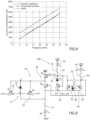
- Figure 8 shows the trend of the current consumption associated with the resonant driver 60, by way of example as a function of the frequency f (assuming that the high voltage VHV is equal to 32 V, the capacitance, here indicated by C LOAD , of the first and the second capacitive actuators is equal to 2 nF and the number N of tank capacitors is equal to 8).
- the solution described for the switch device 20 allows to obtain a rapid turn-on time, thanks in particular to the fact that the parasitic capacitances are not completely discharged during the turn-off phase and also thanks to the fact that the driving current is provided to the bidirectional switch 21 by an n-type MOS in source-follower configuration (the aforementioned driving transistor M ON ).
- the source follower configuration of the driving transistor M ON of driving stage 26 is advantageous from the point of view of the Safe Operating Area (SOA).
- SOA Safe Operating Area
- the turn-off time is also rapid, thanks to the fact that the turn-off condition is obtained by zeroing the voltage between the gate and source terminals of the MOS transistors M1, M2, instead of bringing the corresponding gate terminals to ground.
- the size of the MOS transistors M1 and M2 may possibly be increased, to reduce the on-state resistance (without excessively penalizing the turn-on time).
- the described solution also allows an improvement in power consumption and efficiency, in particular thanks to the fact that the complete discharge of the parasitic capacitances to the ground reference GND is avoided, at each switching from the on-state to the off-state of the switch device.
- the solution described also has a reduced complexity and area occupation compared to known-type solutions.
- Figure 9 shows the switch device 20 wherein a different implementation is adopted for the aforementioned load stage 30.
- this load stage 30 comprises the load zener diode 52, this time having its cathode terminal connected to the input terminal N1 of the load stage 30 and anode terminal connected to the source terminal of the load transistor 50.
- the aforementioned load transistor 50 also in this case of low-voltage NMOS-type, also has gate terminal connected to the input terminal N1 of the load stage 30 and drain terminal connected to the internal node S.
- the load transistor 50 operates in this case in linear region, adding a small voltage drop to the voltage drop on the load zener diode 52, for generating the first driving signal drv_on.
- An advantage represented by this embodiment is that of avoiding the possibility of establishing a direct current path between the internal node S and the supply terminal.
- This embodiment may, for example, be advantageous in case the switch device 20 is used as an anti-ringing switch to short-circuit a corresponding inductance in a DC-DC converter (according to a known solution, not described in detail herein).
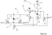
- Figure 10 shows how the control and driving stage 200 of the switch device 20 might be modified (simplified) for this specific application.
- the switch terminal T is in this case connected to a positive power source PVCCA of the DC-DC converter, while the switch terminal A is connected to a switching node SW.
- the switching logic stage 40 may be simplified by the presence of a single low-voltage nMOS-type transistor, indicated by 65, which has its drain terminal connected to the input terminal N1 of the load stage 30 (having the first driving signal drv_on), source terminal connected to the ground reference GND and gate terminal connected to the input terminal N2 of the switching logic stage 40 and receiving in this case the second driving signal drv_off.
- a further low-voltage nMOS-type transistor, indicated by 66 is connected between the internal node S and the same ground reference GND and has its gate terminal connected to the input terminal N2.
- the switch device 20 turns on with respect to the positive power source PVCCA and may be turned off at the ground reference GND.
- the presence of the load zener diode 52 in series with the load transistor 50 avoids a direct current path in turn-off state between the same positive power source PVCCA and the ground reference GND.
- a further implementation of the same load stage 30 might also envisage the absence of the load transistor 50, in this case the value of the first driving signal drv_on being a function of the sole voltage drop on the load zener diode 52. In this case, a greater SoA (Safe Operating Area) might be obtained, at the expense of a lower switching speed.
- SoA Safe Operating Area
- the same load stage 30 might be implemented with further different embodiments, for example with one or more series-connected resistors, with one or more diode-connected MOS transistors, or with other different implementations.
Landscapes
- Electronic Switches (AREA)
Abstract
A switch device (20) is described, formed by: a first switch MOS transistor (22), with its drain terminal connected to a first switch terminal (A), source terminal connected to an internal source node (S) and gate terminal connected to an internal gate node (G); a second switch MOS transistor (24), with its drain terminal connected to a second switch terminal (T), source terminal connected to the internal source node and gate terminal connected to the internal gate node; and a voltage limiting element (25) connected between the internal gate and source nodes. A driving stage (26), voltage-referred to the internal source node, drives the switching of the bidirectional switch, as a function a first and a second driving signals (drv_on, drv_off), and has a driving transistor (MON) and a switching transistor (MOFF), connected to each other; the driving transistor is driven by the first driving signal to charge the internal gate node and turn on the bidirectional switch; and the switching transistor is driven by the second driving signal to short-circuit the internal gate and source nodes and turn off the bidirectional switch.
Description
- The present solution relates to a high-voltage bidirectional switch device with improved electrical characteristics.
- There are several applications in which the use is required of bidirectional high-voltage switch devices, capable of allowing the transfer of current in both directions between a first high-voltage terminal and a second high-voltage terminal.
- By way of example, high-voltage switch devices are commonly used in charge recovery resonant drivers.
- These drivers base the charge recovery on a suitable sharing between a first and a second load capacitive elements (which may correspond to capacitive actuators, for example capacitive micromirrors) by using a certain number of tank and storage capacitors.
- In particular, the sharing of charge between the capacitive elements is achieved according to a specific charge recovery algorithm by means of bidirectional switch devices connected between the same capacitive elements and the storage capacitors, suitably driven by driving signals having a high-voltage (of the order of several tens of V) and average frequencies (up to a few tens of kHz).
- These switch devices are required to manage (bidirectionally) high voltages on both terminals. In particular, to exploit the charge recovery performances, switch devices not only need to have low on-state resistance, but also have turn-on and turn-off times as fast as possible. Furthermore, the energy consumption to drive the switches and the area required to form the corresponding drivers typically need to be minimized.
-
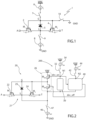
Figure 1 shows a known circuit embodiment of a high-voltage bidirectional switch device, generally indicated by 1. - This
switch device 1 defines a bidirectional switch formed by: afirst switch element 2, in particular a high-voltage MOS transistor M1, having drain terminal connected to a first switch terminal A (e.g., designed to be connected to a first charge redistribution capacitive element), source terminal connected to an internal node S and gate terminal connected to an internal node G. The bulk terminal of the MOS transistor M1 is also connected to the source terminal, in such a way that the parasitic diode (indicated inFigure 1 ) is directed to avoid improper turn-on during operation (in some cases, the connection between bulk and source terminals is intrinsic). - The bidirectional switch is also formed by a
second switch element 4, in particular a high-voltage MOS transistor M2, having drain terminal connected to a second switch terminal T (e.g., designed to be connected to a second charge redistribution capacitive element), source terminal connected to the internal node S and gate terminal connected to the internal node G. As shown inFigure 1 , the MOS transistor M2 also has a bulk terminal connected to the source terminal, as previously discussed. - The aforementioned high-voltage MOS transistors M1, M2 are capable of withstanding high voltages applied between the corresponding drain and source terminals and between the corresponding gate and drain terminals (e.g., with values of the order of 40-60 V, higher, for example of at least one order of magnitude, with respect to low voltage values, e.g., lower than 10 V, in particular about 5 V).
- The
switch device 1 also comprises avoltage limiting element 5 connected between the internal nodes G and S, in particular formed by a zener diode, having anode connected to the aforementioned internal node S and cathode connected to the aforementioned internal node G, and having the function of limiting the voltage between the same internal nodes G and S to a maximum value, for example equal to 5.5 V (that may be withstood between the gate and source terminals by the aforementioned MOS transistors M1, M2). - The
switch device 1 also comprises: a first current generator 6, configured to generate a first current I1, connected between a supply terminal having a high supply voltage VHV (e.g., of the order of tens of V, for example in the range 40-60 V) and the internal node G, with the interposition of afirst switch 7; a second current generator 8, configured to generate a second current 12, connected between the internal node S, with the interposition of a second switch 9, and a ground reference (GND); and furthermore athird switch 10, interposed between the aforementioned internal node G and the ground reference GND. - Operation of the
switch device 1 envisages that thesame switch device 1 is turned on by providing the first and second currents I1 and I2 by closing the first andsecond switches 7, 9, with the aforementionedvoltage limiting element 5 which defines and limits the voltage VGS between gate and source for the MOS transistors M1 and M2; consequently, a current transfer occurs between the first and the second switch terminals A, T (possible in both directions). - The
switch device 1 is turned off removing the first and second currents I1 and I2 by opening the first andsecond switches 7, 9 and also connecting the internal node G (and therefore the gate terminal of the MOS transistors M1 and M2) to the ground reference GND, by closing the third switch 10 (in a manner not illustrated here, the possibility of connecting also the internal node S and therefore the source terminal of the same MOS transistors M1 and M2 to the ground reference GND may also be envisaged); consequently, the current transfer between the first and the second switch terminals A, T is interrupted. - However, this
switch device 1 has some drawbacks. - In the first place, when the
switch device 1 is off, the parasitic capacitances at the internal nodes G and S are totally discharged to the ground reference, so that the same capacitances need to be recharged each time, upon turn-on (with an associated increase in current consumption). - Furthermore, the turn-on currents (the aforementioned first and second currents I1 and I2) are required to have a high value to ensure sufficiently rapid charging times; the circuit designed for their generation is therefore generally complex, has costly manufacture and entails high area occupation in integrated manufacturing.
- Furthermore, these turn-on currents need to be applied for a time which is not known a priori and is variable as a function of parameters such as the process, voltages to be controlled and temperature; the value of these currents is therefore generally oversized to avoid operating issues.
- The aforementioned issues are accentuated by the fact that the switch device is required to have (as previously mentioned) an on-resistance value that is as low as possible in order to maximize the efficiency (for example of an associated charge recovery driver). This may be obtained by increasing its size and (especially in high-voltage domains) this entails a significant increase in parasitic capacitances.
- Some solutions have therefore been proposed aimed at overcoming, at least in part, the issues described above for the
switch device 1. - For example, it has been proposed to limit the application of the turn-on currents only for a short time interval (of initial precharge), at turn-on, followed by a lower holding current. Furthermore, the use of auxiliary switch elements, transistor switch elements, has been proposed, in addition to the aforementioned MOS transistors M1 and M2, also operative in an initial precharge phase.
- However, despite being capable of allowing a reduction in the turn-on times, these solutions generally entail greater complexity and higher power consumption and, in any case, do not overcome some of the issues previously highlighted.
- In general, the need to provide an improved solution for bidirectional switch devices for high voltage applications is certainly felt.
- The aim of the present solution is to overcome, at least in part, the issues previously highlighted and to meet the aforementioned need.
- According to the present solution, therefore, a switch device is provided, as defined in the attached claims.
- For a better understanding of the present invention, a preferred embodiment thereof is now described, purely by way of non-limiting example and with reference to the attached drawings, wherein:
-
Figure 1 shows the circuit diagram of a high-voltage bidirectional switch device, of a known type; -
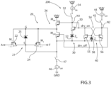
Figure 2 shows the circuit diagram of a high-voltage bidirectional switch device, according to an embodiment of the present solution; -
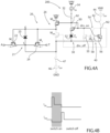
Figure 3 shows a more detailed circuit diagram of the bidirectional switch device ofFigure 2 ; -
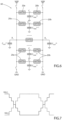
Figure 4A shows the bidirectional switch device ofFigure 3 , with particular reference to a turn-on phase; -
Figure 4B shows a time diagram of turn-on and turn-off currents in the switch device, with particular reference to the aforementioned turn-on phase; -
Figure 5A shows the bidirectional switch device ofFigure 3 , with particular reference to a turn-off phase; -
Figure 5B shows a time diagram of turn-on and turn-off currents in the switch device, with particular reference to the aforementioned turn-off phase; -
Figure 6 shows a schematic circuit diagram of a charge recovery resonant driver wherein the switch device may be used, according to a further aspect of the present solution; -
Figure 7 shows voltage diagrams relating to operation of the driver ofFigure 6 ; -
Figure 8 shows the trend of a current consumption as a function of frequency in the driver ofFigure 6 , compared with known-type solutions; and -
Figures 9-10 show respective circuit diagrams of the bidirectional switch device, in accordance with a different embodiment of the present solution. -
Figure 2 shows a high-voltage bidirectional switch device, generally indicated by 20, according to the present solution. - The
switch device 20 comprises abidirectional switch 21, which is formed, in a substantially analogous manner to what discussed with reference toFigure 1 , by: - a
first switch element 22, in particular a high-voltage MOS transistor M1, having drain terminal connected to a first switch terminal A (e.g., designed to be connected to a first capacitive element, for example to a capacitive actuator), source terminal connected to an internal node S and gate terminal connected to an internal node G; - a
second switch element 24, in particular a high-voltage MOS transistor M2, having drain terminal connected to a second switch terminal T (e.g., designed to be connected to a second capacitive element, in particular to a storage capacitor), source terminal connected to the internal node S and gate terminal connected to the internal node G; and - a
voltage limiting element 25 connected between the internal nodes G and S, in particular formed by a zener diode, having anode connected to the aforementioned internal node S and cathode connected to the aforementioned internal node G, and having the function of limiting the voltage between the same internal nodes G and S to a maximum withstandable value, for example equal to 5.5 V. - The aforementioned high-voltage MOS transistors M1, M2 are capable of withstanding high voltages applied between the corresponding drain and source terminals and between the corresponding gate and drain terminals (for example, of the order of 40-60 V); the voltage between the gate and source terminals is instead limited to the maximum value clamped by the aforementioned
voltage limiting element 25. - According to an aspect of the present solution, the
switch device 20 further comprises a control and driving stage, generally indicated by 200, voltage-referred to the internal node S (as opposed to a ground reference GND) and configured to control and drive switching of thebidirectional switch 21. - This control and
driving stage 200 comprises adriving stage 26, referred to the internal node S and configured to receive at an input first and a second driving signals drv_on, drv_off, both voltage signals (with logically opposite values, i.e. if drv_on is logically high then drv_off is logically low and vice versa), and implement the switching of thebidirectional switch 21 as a function of these first and second driving signals drv_on, drv_off. - In detail, the
driving stage 26 comprises a driving transistor MON and a switching transistor MOFF, both of NMOS-type, driven by the aforementioned first and second driving signals drv_on, drv_off and connected to each other substantially in inverter configuration. - In particular, the driving transistor MON has its drain terminal connected to a supply terminal having a high supply voltage VHV (e.g., of the order of 40-60 V), gate terminal which receives the first driving signal drv_on and source terminal connected to the aforementioned internal node G (furthermore, the source terminal is connected to the corresponding bulk terminal, for correctly biasing the junctions in each operating condition).
- The switching transistor MOFF has its drain terminal connected to the aforementioned internal node G, gate terminal which receives the second driving signal drv_off and source terminal connected to the aforementioned internal node S (the source terminal is also connected to the corresponding bulk terminal).
- In greater detail, the driving transistor MON, referred to the high supply voltage VHV, is configured to operate as a source-follower and is driven by the first driving signal drv_on to charge the internal node G (and therefore the gate terminals of the MOS transistors M1 and M2) in a fast and efficient manner and thereby turn on the bidirectional switch 21 (allowing the current or charge transfer between the corresponding terminals A and T, in both directions); this configuration is also advantageously self-limited in current.
- The switching transistor MOFF is driven by the second driving signal drv_off to short-circuit, when driven in the on-state, the internal nodes G and S (and therefore the gate and source terminals of the MOS transistors M1 and M2), thereby turning off the bidirectional switch 21 (it should be noted that, unlike known solutions, the gate and/or source terminals of the same MOS transistors M1 and M2 are not connected in this case to the ground reference GND during operation of the
switch device 20, in particular for turning off the bidirectional switch 21). - The control and
driving stage 200 of theswitch device 20 further comprises aload stage 30, also referred to the internal node S and having an input terminal N1 selectively connectable, by afirst switch 32, to a turn-oncurrent generator 34, configured to generate a turn-on current ION and in turn connected to the supply terminal (and to the high voltage VHV). - The
aforementioned load stage 30 is configured to generate, through the turn-on current ION, the first driving signal drv_on, being a voltage signal, to cause turn-on of the driving transistor MON of thedriving stage 26. - The control and
driving stage 200 of theswitch device 20 also comprises aswitching logic stage 40, also referred to the internal node S and having a respective input terminal N2 selectively connectable, by asecond switch 42, to a turn-offcurrent generator 44, configured to generate a turn-off current IOFF and in turn connected to the supply terminal (and to the high voltage VHV). - This
switching logic stage 40 is configured to generate, on the basis of the turn-off current IOFF and the value of the first driving signal drv_on, the second driving signal drv_off, being a voltage signal, to cause turn-on of the switching transistor MOFF of thedriving stage 26. - As will also be discussed in detail hereinbelow, the second driving signal drv_off which (when logically high) allows the switching transistor MOFF to be turned on is generated by the turn-off current IOFF and by switching of the first driving signal drv_on to the low logic value, in turn generated by turning off the turn-on current ION. The driving signals drv_on, drv_off which determine turn-on and turn-off of the driving and switching transistors MON and MOFF are therefore controlled by the turn-on and turn-off currents ION and IOFF (in turn determined by the activation, logically alternative, of the corresponding switches 32, 42). Substantially, when it is desired to switch on the driving transistor MON, the turn-on current ION is activated and the turn-off current IOFF is deactivated; consequently, the first driving signal drv_on goes to the high logic state and the second driving signal drv_off to the low logic state. Conversely, when it is desired to switch on the turn-off transistor MOFF, the turn-off current IOFF is activated and the turn-on current ION is deactivated; consequently, the second driving signal drv_off goes to the high logic state and the first driving signal drv_on to the low logic state.
- The aforementioned control and driving
stage 200 may also comprise, as shown in the aforementionedFigure 2 , a further turn-offcurrent generator 46, configured to generate the tun-off current IOFF and connectable between the internal node S (by a third switch 47) and the ground reference GND. As will also be discussed hereinbelow, this further turn-offcurrent generator 46, if present, is configured to compensate for the turn-off current IOFF used by the aforementionedswitching logic stage 40. - During operation, the driving
stage 26 behaves like an N-type inverter, referred to the internal node S, thus operating in a floating manner with respect to the ground reference GND. - Turn-on requires a small value of the turn-on current ION (since this current only needs to charge the parasitic capacitance of the driving transistor MON and of the load), which determines the generation, by the
load stage 30, of a suitable value of the first driving signal drv_on, such as to cause turn-on of the driving transistor MON of the drivingstage 26. - In particular, during turn-on, by supplying a voltage to the gate terminal of the driving transistor MON through the turn-on current ION and the
load stage 30, the source terminal of the same driving transistor MON (which corresponds to the aforementioned internal node G) follows the potential of the corresponding gate terminal, minus the threshold voltage. In this way, a desired voltage is imposed between internal nodes G and S (designed to properly turn on MOS transistors M1 and M2 of bidirectional switch 21). This is advantageously implemented with a high current capability (a prerogative of the source-follower configuration) because the driving transistor MON, referenced to the high voltage VHV, operates in transient with a high voltage between gate and source VGS and thus is capable of delivering a high current. - The turn-off is obtained by short-circuiting the source and gate terminals of the MOS transistors M1 and M2, as opposed to bringing (as in known solutions) the same terminals to the ground reference GND. In turn-off state, both the
first switch element 22 and thesecond switch element 24 remain in a totally floating state, thus following the dynamics of the capacitive elements connected to the switch terminals A and T. Substantially, the parasitic capacitances are therefore not completely discharged towards ground, but undergo at most a limited discharge, corresponding to the loss of voltage between gate and source (VGS), due to turn-off of the aforementioned transistors M1 and M2. - It should be noted that, in a manner not illustrated in detail (but which will be evident to a person skilled in the art), the
aforementioned switch device 20 is configured to receive from the outside (e.g. from a control unit of an electronic device wherein thesame switch device 20 is used) suitable control signals, in particular for driving the first, second andthird switches - Referring now to
Figure 3 , a first embodiment of the control and drivingstage 200 of theswitch device 20 is now described in greater detail, in particular with respect to theaforementioned load stage 30 and the aforementionedswitching logic stage 40. - In the illustrated embodiment, the
load stage 30 comprises aload transistor 50, of low-voltage NMOS-type, and aload zener diode 52, connected in series with theload transistor 50, having anode terminal connected to the internal node S and cathode terminal connected to the source terminal of theaforementioned load transistor 50. Thisload transistor 50 also has gate terminal connected to the corresponding drain terminal (being therefore diode-connected) and also to the input terminal N1 of theload stage 30, i.e. to the gate terminal of the driving transistor MON of the drivingstage 26, at which the first driving signal drv_on is generated (theaforementioned load transistor 50 also has a source terminal connected to the bulk terminal). - The switching
logic stage 40 comprises aMOS latch 54 having the input terminals N1, N2 as input/output terminals and referred to the internal node S. This switchinglogic stage 40 is formed by a first and asecond latch transistor - the
first latch transistor 55, of low-voltage nMOS-type, has its drain terminal connected to the input terminal N1 of the load stage 30 (having the first driving signal drv_on), source terminal connected to the internal node S and gate terminal connected to the input terminal N2 of the switching logic stage 40 (and to the drain terminal of the second latch transistor 56); and - the
second latch transistor 56, of low-voltage nMOS-type, has its drain terminal connected to the input terminal N2 of the switchinglogic stage 40, source terminal connected to the internal node S and gate terminal connected to the input terminal N1 of the load stage 30 (and to the drain terminal of the first latch transistor 55). - The
aforementioned latch transistors - The switching
logic stage 40 further comprises azener diode 58, having anode connected to the internal node S and cathode connected to the input terminal N2 (and to the gate terminal of thefirst latch transistor 55 and drain terminal of the second latch transistor 56). - As will also be highlighted hereinbelow, the
MOS latch 54, referred to the internal node S, allows to speed up switching from the on-state to the off-state (and vice versa) and to maintain the aforementioned on- and off-states of thebidirectional switch 21 with a minimum current request. - During operation, also referring to
Figure 4A (which highlights the portion of theswitch device 20 referred to the turn-on state) and also to the timing diagrams ofFigure 4B , a pulse of turn-on current ION at a first precharge value determines generation, by theload stage 30, of the driving signal drv_on, for turning on the driving transistor MON of the driving stage 26 (and turning on the bidirectional switch 21) . - In particular, in the embodiment described, the value of the driving signal drv_on, referred to the internal node S, is given by the sum of the voltage VZD on the
load zener diode 52 and the gate-source voltage VGS(50) of the load transistor 50 (diode-connected):
- The driving transistor MON of the driving
stage 26 turns on with a gate-source voltage VGS(MON) substantially equal to VZD, assuming that the same driving transistor MON is matched to the load transistor 50 (it should be noted that, to optimize this matching, theload transistor 50 may be implemented as a high-voltage transistor, with a minimum penalty in terms of power and area consumption). - In particular, with the circuit solution shown in the above
Figure 3 , since theload transistor 50 and the driving transistor MON have similar threshold voltage, the voltage of a zener diode is basically applied between the internal nodes G and S, i.e., a sufficiently high and well-defined voltage for driving thebidirectional switch 21. - The
second latch transistor 56 also turns on, thus bringing the second driving signal drv_off to the value of the internal node S and thereby turning off the switching transistor MOFF (and also the first latch transistor 55). - Advantageously, the turn-on time of the
bidirectional switch 21 is very fast, thanks in particular to the source-follower configuration of the driving transistor MON and to the small charge which needs to be provided to charge the parasitic capacitances. The turn-on current ION depends on the size of the same driving transistor MON and may be easily optimized with respect to the parasitic capacitances to be charged. Furthermore, the turn-on current ION which is provided in excess (in any case for a limited time, determined by the precharge pulse) is "recycled" on the capacitive elements (for example load and storage elements) connected to the first and second switch terminals A and T of thebidirectional switch 21. - Subsequently, the turn-on condition may be maintained for a second value of the turn-on current ION, being a holding value, lower than the aforementioned first precharge value (as shown in the aforementioned
Figure 4B ), exploiting the positive feedback offered by theMOS latch 54. This holding current is essentially required to be sufficient to reinforce the positive feedback offered by theMOS latch 54 to compensate for parasitic effects (couplings, ground and reference movements) which might lead to an improper switching of the same latch. - Referring now to
Figure 5A (which highlights the portion of theswitch device 20 referred to the turn-off state) and to the timing diagrams ofFigure 5B , the turn-off phase of thebidirectional switch 21 envisages removal of the turn-on current ION (which goes to a null value) and the provision of the turn-off current IOFF, having a respective pulse at a first precharge value (followed by a holding value, lower than the aforementioned first value, which is maintained throughout the entire duration of the turn-off phase). - Following the provision of the aforementioned turn-off current IOFF, the second driving signal drv_off increases with respect to the internal node S up to a value VZL, equal to the voltage across the
zener diode 58. - Consequently, the switching transistor MOFF turns on, with a voltage between the corresponding gate and source terminals VGS(MOFF) equal to the same value VZL. Furthermore, the
first latch transistor 55 turns on, to bring the first driving signal drv_on to the value of the internal node S and thereby turn off the driving transistor MON. - Given that, typically, the turn-off state has a longer duration with respect to the turn-on state, it may also be envisaged that a current matched to the aforementioned turn-off current IOFF is extracted from the internal node S by the further turn-off current generator 46 (with the
third switch 47 closed), in such a way as to compensate for the current required to maintain the state of theMOS latch 54 and not influence the voltage values present at the first and the second switch terminals A, T of thebidirectional switch 21. - With reference to
Figure 6 , a possible application of theaforementioned switch device 20 is now described, in a charge recovery resonant driver, generally indicated by 60. - This
resonant driver 60 operates to exchange electric charge between a first capacitive actuator COUT(1), coupled to a first charge exchange terminal A1, which is selectively alternately connectable to a supply terminal having a high-voltage VHV and a ground reference terminal GND; and a second capacitive actuator COUT(2), coupled to a second charge exchange terminal A2, which is also selectively alternately connectable to the supply terminal having the high voltage VHV and the ground reference terminal GND. - The
resonant driver 60 comprises a plurality N of tank capacitors, indicated by CTANK(1)... CTANK(N), which may be selectively connected to the first or the second charge exchange terminal A1, A2, by afirst switch device 20a, respectively by asecond switch device 20b (coupled to each other at a respective internal node C1... CN, having the respective tank capacitors CTANK(1)... CTANK(N) connected thereto). - In particular, each of the aforementioned first and
second switch devices switch device 20. - Advantageously, the floating condition, in turn-off state, of both the
first switch element 22 and thesecond switch element 24 of eachswitch device 20 causes the gate and source terminals of the corresponding MOS transistors M1 and M2 to follow the trend of the switch terminals A and T to maintain a bias condition always close to that of the (next) turn-on. In terms of charge, this means that the parasitic capacitances of the switches "participate" in the charge redistribution (significantly reducing the lost charge). The advantage of the proposed solution is therefore twofold: no charge is lost by continuing to charge and discharge the parasitic capacitances, and the switch is made to be close, before turning on, to the bias condition that it will have during the same turn-on, thus minimizing turn-on time. - By suitably driving the aforementioned first and
second switch devices Figure 7 . - In particular, it has been demonstrated that the power consumption associated with the
resonant driver 60 is reduced by a theoretical factor N (being equal to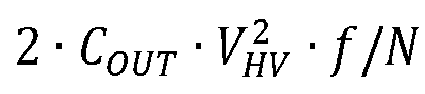
- However, this factor N is generally reduced by the power consumption required for driving the
switch devices - The present Applicant has instead demonstrated the possibility of substantially reaching the ideal value for the aforementioned factor N thanks to the use of the solution previously described in detail for providing the
aforementioned switch devices - In this regard,
Figure 8 shows the trend of the current consumption associated with theresonant driver 60, by way of example as a function of the frequency f (assuming that the high voltage VHV is equal to 32 V, the capacitance, here indicated by CLOAD, of the first and the second capacitive actuators is equal to 2 nF and the number N of tank capacitors is equal to 8). - In particular, the ideal current consumption (equal to 2·COUT ·VHV ·f/N) is indicated in dashed line; the current consumption obtainable with a solution of known-type (wherein switch devices of traditional type are used, for example of the type shown in
Figure 1 ) are indicated in dash-dot line; and the current consumption obtainable using theswitch devices 20 according to the present solution is indicated in solid line. - It is therefore clear that the solution described for the
aforementioned switch devices 20 allows to achieve a current consumption substantially equivalent to the ideal consumption. - The advantages of the proposed solution are clear from the preceding description.
- In any case, it is highlighted that the solution described for the
switch device 20 allows to obtain a rapid turn-on time, thanks in particular to the fact that the parasitic capacitances are not completely discharged during the turn-off phase and also thanks to the fact that the driving current is provided to thebidirectional switch 21 by an n-type MOS in source-follower configuration (the aforementioned driving transistor MON). - Moreover, the source follower configuration of the driving transistor MON of driving
stage 26 is advantageous from the point of view of the Safe Operating Area (SOA). Such a driving transistor MON has a controlled voltage between gate and source VGS; moreover, using a high voltage device to implement the same driving transistor MON, the voltage VDS between drain and source terminals can be easily protected. - Furthermore, the turn-off time is also rapid, thanks to the fact that the turn-off condition is obtained by zeroing the voltage between the gate and source terminals of the MOS transistors M1, M2, instead of bringing the corresponding gate terminals to ground.
- At the same time, given the efficiency in controlling the parasitic capacitances, the size of the MOS transistors M1 and M2 may possibly be increased, to reduce the on-state resistance (without excessively penalizing the turn-on time).
- The described solution also allows an improvement in power consumption and efficiency, in particular thanks to the fact that the complete discharge of the parasitic capacitances to the ground reference GND is avoided, at each switching from the on-state to the off-state of the switch device.
- The solution described also has a reduced complexity and area occupation compared to known-type solutions.
- Finally, it is clear that modifications and variations may be made to what has been described and illustrated herein without thereby departing from the scope of the present invention, as defined in the attached claims.
- In particular, it is emphasized that different circuit implementations may be envisaged for both the
load stage 30 and for the switchinglogic stage 40 of theswitch device 20. - For example,
Figure 9 shows theswitch device 20 wherein a different implementation is adopted for theaforementioned load stage 30. - In this embodiment, this
load stage 30 comprises theload zener diode 52, this time having its cathode terminal connected to the input terminal N1 of theload stage 30 and anode terminal connected to the source terminal of theload transistor 50. - The
aforementioned load transistor 50, also in this case of low-voltage NMOS-type, also has gate terminal connected to the input terminal N1 of theload stage 30 and drain terminal connected to the internal node S. - In turn-on condition, the
load transistor 50 operates in this case in linear region, adding a small voltage drop to the voltage drop on theload zener diode 52, for generating the first driving signal drv_on. - An advantage represented by this embodiment is that of avoiding the possibility of establishing a direct current path between the internal node S and the supply terminal.
- This embodiment may, for example, be advantageous in case the
switch device 20 is used as an anti-ringing switch to short-circuit a corresponding inductance in a DC-DC converter (according to a known solution, not described in detail herein). - In this regard,
Figure 10 shows how the control and drivingstage 200 of theswitch device 20 might be modified (simplified) for this specific application. - In particular, the switch terminal T is in this case connected to a positive power source PVCCA of the DC-DC converter, while the switch terminal A is connected to a switching node SW.
- The switching
logic stage 40 may be simplified by the presence of a single low-voltage nMOS-type transistor, indicated by 65, which has its drain terminal connected to the input terminal N1 of the load stage 30 (having the first driving signal drv_on), source terminal connected to the ground reference GND and gate terminal connected to the input terminal N2 of the switchinglogic stage 40 and receiving in this case the second driving signal drv_off. A further low-voltage nMOS-type transistor, indicated by 66, is connected between the internal node S and the same ground reference GND and has its gate terminal connected to the input terminal N2. - In this case, the
switch device 20 turns on with respect to the positive power source PVCCA and may be turned off at the ground reference GND. As previously indicated, the presence of theload zener diode 52 in series with theload transistor 50 avoids a direct current path in turn-off state between the same positive power source PVCCA and the ground reference GND. - A further implementation of the
same load stage 30 might also envisage the absence of theload transistor 50, in this case the value of the first driving signal drv_on being a function of the sole voltage drop on theload zener diode 52. In this case, a greater SoA (Safe Operating Area) might be obtained, at the expense of a lower switching speed. - In general, the
same load stage 30 might be implemented with further different embodiments, for example with one or more series-connected resistors, with one or more diode-connected MOS transistors, or with other different implementations.
Claims (18)
- A switch device (20), comprising a bidirectional switch (21), formed by:a first switch MOS transistor (22), having its drain terminal connected to a first switch terminal (A), source terminal connected to an internal source node (S) and gate terminal connected to an internal gate node (G);a second switch MOS transistor (24), having its drain terminal connected to a second switch terminal (T), source terminal connected to the internal source node (S) and gate terminal connected to the internal gate node (G); anda voltage limiting element (25) connected between the internal gate and source nodes (G, S),wherein said switch device (20) further comprises a driving stage (26), voltage-referred to the internal source node (S) and configured to drive switching of the bidirectional switch (21), as a function of a first and a second driving signals (drv_on, drv_off), said driving stage (26) comprising a driving transistor (MON) and a switching transistor (MOFF), connected to each other;wherein said driving transistor (MON) is connected to a supply terminal and is driven by the first driving signal (drv_on) to charge the internal gate node (G) and turn on the bidirectional switch (21) in a turn-on interval of said switch device (20); and said switching transistor (MOFF) is driven by the second driving signal (drv_off) to short-circuit the internal gate and source nodes and turn off the bidirectional switch (21) in a turn-off interval of said switch device (20).
- The device according to claim 1, wherein said driving transistor (MON) is an n-type MOS transistor in source-follower configuration.
- The device according to claim 2, wherein said driving transistor (MON) has its drain terminal connected to the supply terminal, gate terminal receiving the first driving signal (drv_on) and source terminal connected to the aforementioned internal gate node (G); and said switching transistor (MOFF) has its drain terminal connected to the internal gate node (G), gate terminal receiving the second driving signal (drv_off) and source terminal connected to the internal source node (S).
- The device according to any of the preceding claims, wherein during said turn-off interval of said switch device (20), the first and second switch MOS transistors (22, 24) of said bidirectional switch (21) are in a floating state.
- The device according to any of the preceding claims, further comprising a load stage (30), voltage-referred to the internal source node (S) and having an input terminal (N1) selectively connectable, by a first switch (32) to a turn-on current generator (34), configured to generate a turn-on current (ION); wherein said load stage (30) is configured to generate, through the turn-on current (ION), the first driving signal (drv_on), being a voltage signal, for causing turn-on of the driving transistor (MON) of the driving stage (26) .
- The device according to claim 5, wherein said load stage (30) comprises a load transistor (50) and a load zener diode (52), connected in series with the load transistor (50), having anode terminal connected to the internal source node (S) and cathode terminal connected to the source terminal of the load transistor (50); said load transistor (50) having its gate terminal connected to the corresponding drain terminal, being therefore diode-connected, and also to the input terminal (N1) of the load stage (30).
- The device according to claim 5, wherein said load stage (30) comprises a load transistor (50) and a load zener diode (52), having its cathode terminal connected to the input terminal (N1) of the load stage (30) and anode terminal connected to the source terminal of the load transistor (50); wherein said load transistor (50) has its gate terminal connected to the input terminal (N1) of the load stage (30) and drain terminal connected to the internal source node (S) .
- The device according to claim 6 or 7, wherein said load transistor (50) is of a low-voltage NMOS-type.
- The device according to any of claims 5-8, further comprising a switching logic stage (40), voltage-referred to the internal source node (S) and having a respective input terminal (N2) selectively connectable, by a second switch (42), to a turn-off current generator (44), configured to generate a turn-off current (IOFF); wherein said switching logic stage (40) is configured to generate, based on the turn-off current (IOFF) and the value of the first driving signal (drv_on), said second driving signal (drv_off), being a voltage signal, for causing turn-on of the switching transistor (MOFF) of the driving stage (26).
- The device according to claim 9, wherein the second driving signal (drv_off), with a high logic value, is designed to turn on the switching transistor (MOFF) and is generated based on the turn-off current (IOFF) and the switching to a low logic value of the first driving signal (drv_on), generated by turning-off of the turn-on current (ION); said first and second driving signals (drv_on, drv_off), for determining switching on/off of the driving and switching transistors (MON, MOFF), thus being controlled through the turn-on and turn-off currents (ION, IOFF), in turn determined by the activation, logically alternative, of the corresponding first and second switches (32, 42).
- The device according to claim 9 or 10, wherein said switching logic stage (40) comprises a MOS latch (54) having said input terminals (N1, N2) as input/output terminals and referred to the internal source node (S); said MOS latch (54) being formed by a first and a second latch transistors (55, 56), in cross-configuration, connected between said respective input terminal (N2) and said internal source node (S); and a zener diode (58), having its anode connected to the internal source node (S) and cathode connected to the respective input terminal (N2).
- The device according to claim 11, wherein said MOS latch (54) comprises:a first latch transistor (55), having its drain terminal connected to the load stage (30) and on which said first driving signal (drv_on) is present, source terminal connected to the internal source node (S) and gate terminal connected to the respective input terminal (N2) of said switching logic stage (40); anda second latch transistor (56), having its drain terminal connected to the respective input terminal (N2) of the switching logic stage (40), source terminal connected to the internal source node (S) and gate terminal connected to the drain terminal of the first latch transistor (55).
- The device according to claim 12, wherein said first and second latch transistors (55, 56) are low-voltage nMOS-type transistors.
- The device according to any of claims 9-13, further comprising a further turn-off current generator (46), configured to generate the turn-off current (IOFF) and selectively connected between the internal source node (S), by a third switch (47), and a ground reference (GND).
- The device according to claim 9 or 10, wherein said switching logic stage (40) comprises a low-voltage nMOS transistor (65), having its drain terminal connected to the input terminal (N1) of the load stage (30), source terminal connected to a ground reference (GND) and gate terminal connected to the respective input terminal (N2) of the switching logic stage (40) and receiving the second driving signal (drv_off); wherein a further low-voltage nMOS transistor (66) is connected between the internal source node (S) and said ground reference (GND) and has its gate terminal connected to said respective input terminal (N2).
- The device according to any of the preceding claims, wherein said supply terminal is a high voltage terminal (VHV) and said driving transistor (MON) is a high voltage transistor.
- A charge recovery resonant driver (60) configured to exchange electric charge between a first capacitive actuator (COUT1), coupled to a first charge exchange terminal (A1), selectively alternately connectable to a supply terminal having a high voltage (VHV) and a ground reference terminal (GND); and a second capacitive actuator (COUT2), coupled to a second charge exchange terminal (A2), selectively alternately connectable to the supply terminal and the ground reference terminal (GND); said resonant driver (60) comprising a plurality (N) of tank capacitors (CTANK(1)... CTANK(N)), selectively connected to the first or the second charge exchange terminals (A1, A2), by a first switch device (20a), respectively by a second switch device (20b); wherein each of said first and second switch devices (20a, 20b) is implemented as the switch device (20) according to any of claims 1-13.
- The driver according to claim 17, wherein said first and second capacitive actuators (COUT1, COUT2) are capacitive micromirrors.
Applications Claiming Priority (1)
| Application Number | Priority Date | Filing Date | Title |
|---|---|---|---|
| IT102023000012555A IT202300012555A1 (en) | 2023-06-19 | 2023-06-19 | HIGH VOLTAGE BIDIRECTIONAL SWITCH DEVICE WITH IMPROVED ELECTRICAL CHARACTERISTICS |
Publications (1)
| Publication Number | Publication Date |
|---|---|
| EP4482034A1 true EP4482034A1 (en) | 2024-12-25 |
Family
ID=87801673
Family Applications (1)
| Application Number | Title | Priority Date | Filing Date |
|---|---|---|---|
| EP24179551.7A Pending EP4482034A1 (en) | 2023-06-19 | 2024-06-03 | High-voltage bidirectional switch device with improved electrical characteristics |
Country Status (4)
| Country | Link |
|---|---|
| US (1) | US20240421809A1 (en) |
| EP (1) | EP4482034A1 (en) |
| CN (1) | CN119171894A (en) |
| IT (1) | IT202300012555A1 (en) |
Citations (2)
| Publication number | Priority date | Publication date | Assignee | Title |
|---|---|---|---|---|
| EP1860775A1 (en) * | 2006-05-26 | 2007-11-28 | STMicroelectronics S.r.l. | Driving configuration of a switch |
| US20160043720A1 (en) * | 2014-08-07 | 2016-02-11 | Hitachi, Ltd. | Semiconductor integrated circuit device |
Family Cites Families (4)
| Publication number | Priority date | Publication date | Assignee | Title |
|---|---|---|---|---|
| JP5363511B2 (en) * | 2011-01-14 | 2013-12-11 | 利康 鈴木 | Multi-valued logic circuit |
| CN110870192B (en) * | 2016-10-28 | 2021-11-12 | 因特莱索有限责任公司 | Load identification AC power supply with control and method |
| US10277205B1 (en) * | 2018-06-05 | 2019-04-30 | Samsung Electronics Co., Ltd. | SPDT switch with high linearity |
| US11146267B1 (en) * | 2020-11-30 | 2021-10-12 | Stmicroelectronics S.R.L. | Charge recovery driver for MEMS mirror with reduced number of tank capacitors |
-
2023
- 2023-06-19 IT IT102023000012555A patent/IT202300012555A1/en unknown
-
2024
- 2024-06-03 EP EP24179551.7A patent/EP4482034A1/en active Pending
- 2024-06-11 US US18/740,272 patent/US20240421809A1/en active Pending
- 2024-06-14 CN CN202410769072.6A patent/CN119171894A/en active Pending
Patent Citations (2)
| Publication number | Priority date | Publication date | Assignee | Title |
|---|---|---|---|---|
| EP1860775A1 (en) * | 2006-05-26 | 2007-11-28 | STMicroelectronics S.r.l. | Driving configuration of a switch |
| US20160043720A1 (en) * | 2014-08-07 | 2016-02-11 | Hitachi, Ltd. | Semiconductor integrated circuit device |
Also Published As
| Publication number | Publication date |
|---|---|
| IT202300012555A1 (en) | 2024-12-19 |
| CN119171894A (en) | 2024-12-20 |
| US20240421809A1 (en) | 2024-12-19 |
Similar Documents
| Publication | Publication Date | Title |
|---|---|---|
| US11336193B2 (en) | Isolated DC-DC converter | |
| US9806616B2 (en) | Control circuit for multiple high side switches | |
| US8907641B2 (en) | Circuit and method for short circuit protection | |
| CN110460226B (en) | Switching power supply device | |
| EP3907888B1 (en) | A circuit to transfer a signal between different voltage domains and corresponding method to transfer a signal | |
| JP4712519B2 (en) | Charge pump circuit for high side drive circuit and driver drive voltage circuit | |
| EP1654804B1 (en) | High frequency control of a semiconductor switch | |
| US20190379272A1 (en) | Methods, apparatus, and system to provide a high-efficiency drive for a floating power device | |
| CN113169730A (en) | Driving a D-type FET with a half-bridge driver configuration | |
| US10116292B2 (en) | IGBT gate driving circuit | |
| US20100202163A1 (en) | Flyback power converters | |
| JP2022135911A (en) | Bipolar pulse voltage gate driver | |
| US8390337B2 (en) | Electronic device and method for DC-DC conversion | |
| US10860042B2 (en) | Method of forming a semiconductor device | |
| US20240421809A1 (en) | High-voltage bidirectional switch device with improved electrical characteristics | |
| US7218538B2 (en) | Power source device | |
| WO2024189050A1 (en) | Isolated dc/dc converter and power electronics system | |
| JP5306730B2 (en) | Half bridge circuit | |
| TW201916559A (en) | Control circuit for controlling dead-time of direct current to direct current converter | |
| JP2010022093A (en) | Half bridge circuit | |
| US12362739B2 (en) | Driver circuit and method for controlling a switching element | |
| JP2017112465A (en) | Gate drive circuit | |
| CN115021534B (en) | Gate driver circuit, power supply circuit and method | |
| CN113746305B (en) | Gate driving circuit and multiphase intelligent power module | |
| TW202324895A (en) | Multi-voltage bootstrapping drivers |
Legal Events
| Date | Code | Title | Description |
|---|---|---|---|
| PUAI | Public reference made under article 153(3) epc to a published international application that has entered the european phase |
Free format text: ORIGINAL CODE: 0009012 |
|
| STAA | Information on the status of an ep patent application or granted ep patent |
Free format text: STATUS: THE APPLICATION HAS BEEN PUBLISHED |
|
| AK | Designated contracting states |
Kind code of ref document: A1 Designated state(s): AL AT BE BG CH CY CZ DE DK EE ES FI FR GB GR HR HU IE IS IT LI LT LU LV MC ME MK MT NL NO PL PT RO RS SE SI SK SM TR |
|
| STAA | Information on the status of an ep patent application or granted ep patent |
Free format text: STATUS: REQUEST FOR EXAMINATION WAS MADE |
|
| 17P | Request for examination filed |
Effective date: 20250625 |